

Appl. Sci., Volume 7, Issue 3 (March 2017) – 101 articles
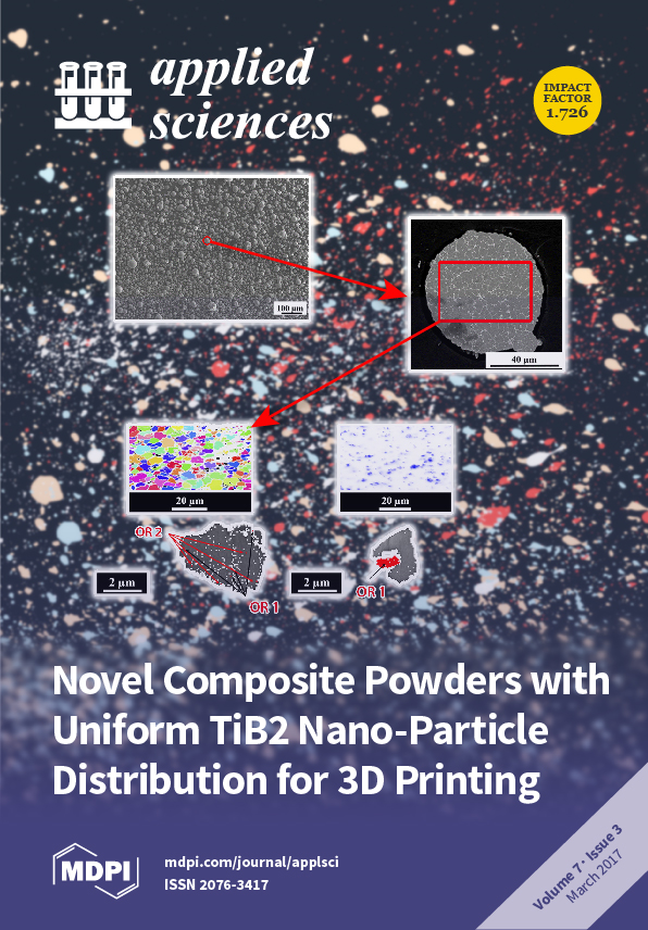
Cover Story (view full-size image):
One of the major challenges in the laser-based additive manufacturing is the severe limitation on powder materials with acceptable laser processability, especially for Al Alloy. We design Al composite powders with TiB2 nanoparticles dispersed within the matrix via gas atomization, thanks to its fast cooling rate and coherent orientation relationship between TiB2 particle and surrounding Al matrix. The introduction of pre-embedded nanometer-sized TiB2 into the Al matrix would help to expand the Al powder palette for AM due to the higher laser absorptivity of TiB2, since the alloy composition of the powders can be easily modified. View the paper
- Issues are regarded as officially published after their release is announced to the table of contents alert mailing list.
- You may sign up for e-mail alerts to receive table of contents of newly released issues.
- PDF is the official format for papers published in both, html and pdf forms. To view the papers in pdf format, click on the "PDF Full-text" link, and use the free Adobe Reader to open them.
Previous Issue
Next Issue