


Membranes, Volume 11, Issue 11 (November 2021) – 110 articles
Cover Story (view full-size image):
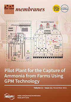
Ammonia emissions from intensive livestock farming are a source of public concern. Their reduction through the application of best available techniques alone may be insufficient to meet environmental goals, which makes technologies that simultaneously reduce NH3 emissions and allow N recovery particularly important. In this work, an NH3-capture prototype, based on the use of expanded polytetrafluoroethylene gas-permeable membranes, was tested in real conditions in a gestating sow house and a free-range laying hen house. Differences were observed between seasons and farms. Given that the limiting factor for the capture process was the NH3 concentration in the air, with the highest recovery occurring in the most concentrated atmosphere, possible scenarios for the application of this emerging technology are proposed. View this paper
- Issues are regarded as officially published after their release is announced to the table of contents alert mailing list.
- You may sign up for e-mail alerts to receive table of contents of newly released issues.
- PDF is the official format for papers published in both, html and pdf forms. To view the papers in pdf format, click on the "PDF Full-text" link, and use the free Adobe Reader to open them.
Previous Issue
Next Issue