
A Novel Nitrogen Ion Implantation Technique for Turning Thin Film “Normally On” AlGaN/GaN Transistor into “Normally Off” Using TCAD Simulation


Abstract
:1. Introduction
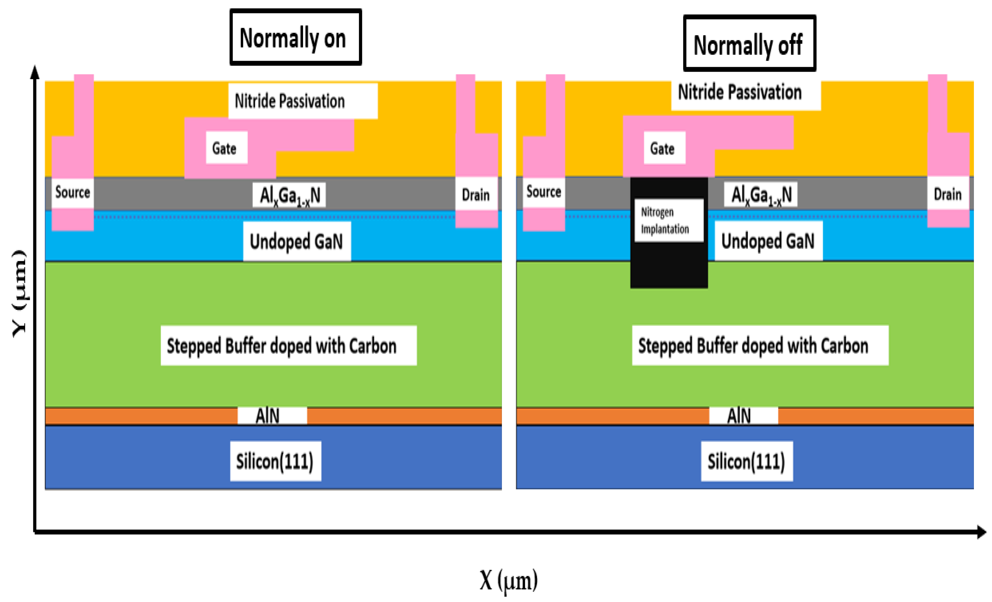
2. Device Structure and Simulation Setup
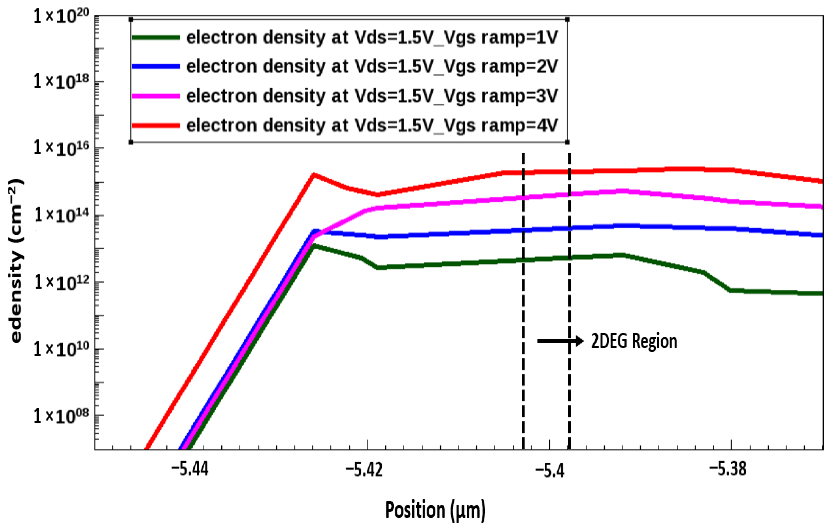
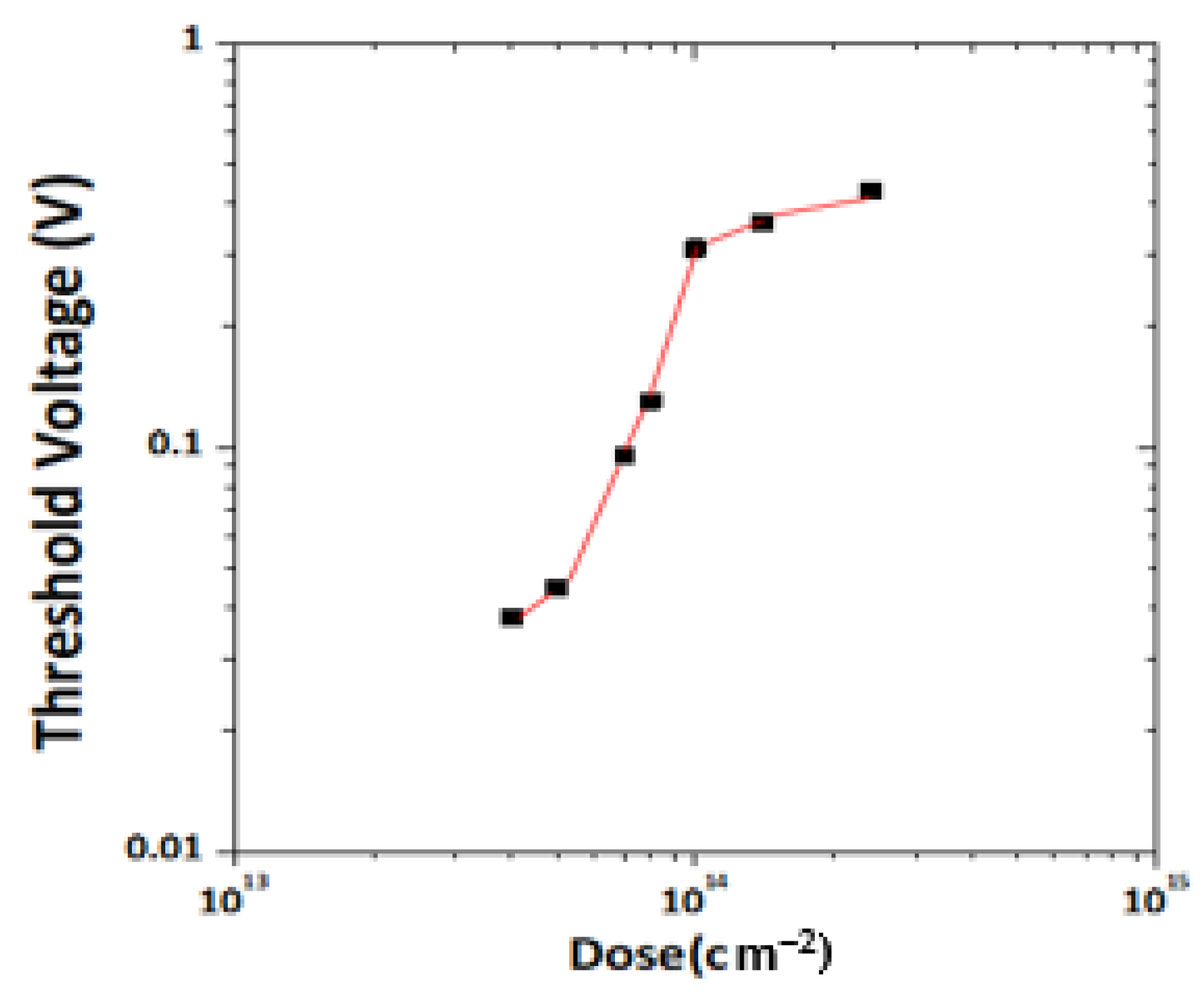
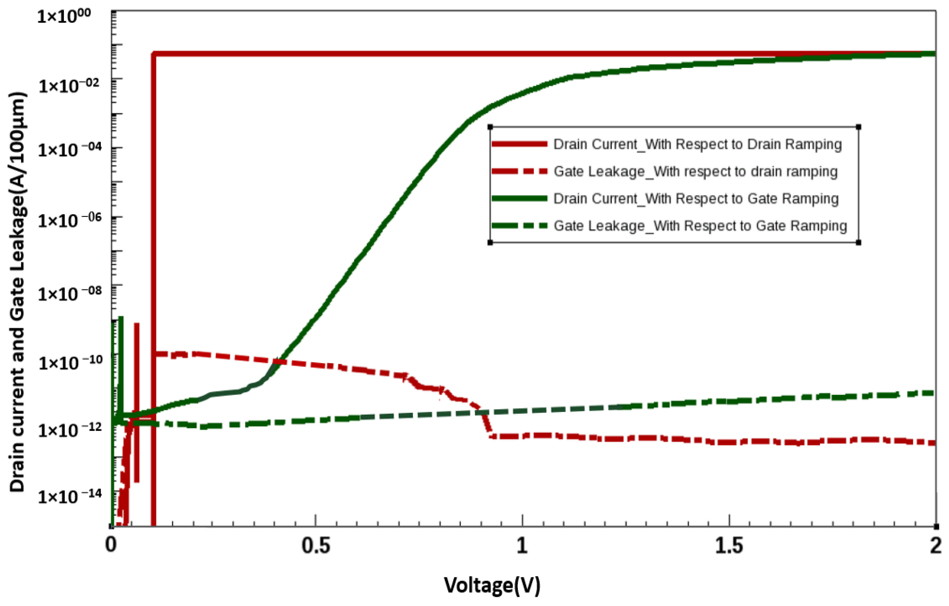
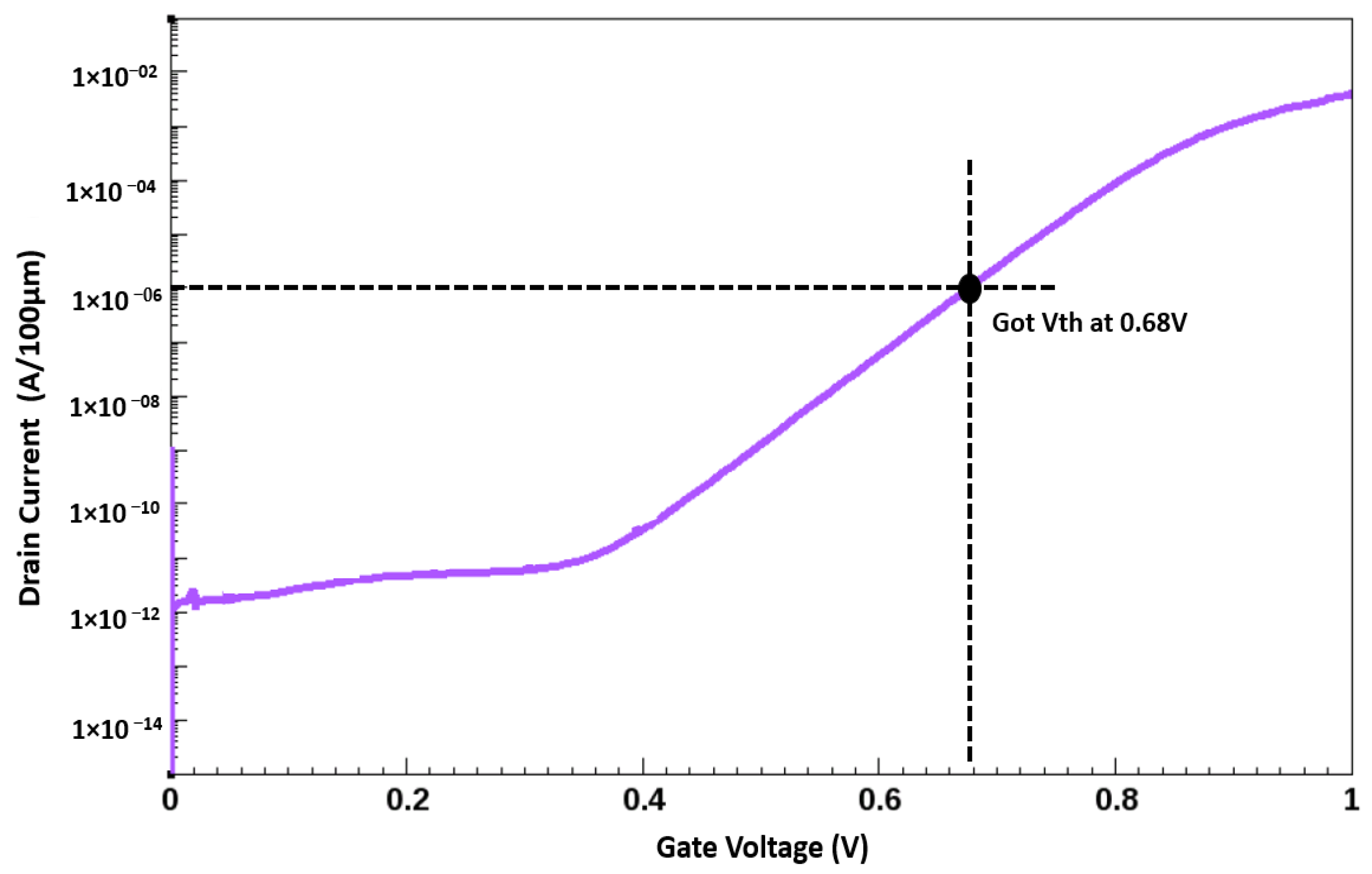
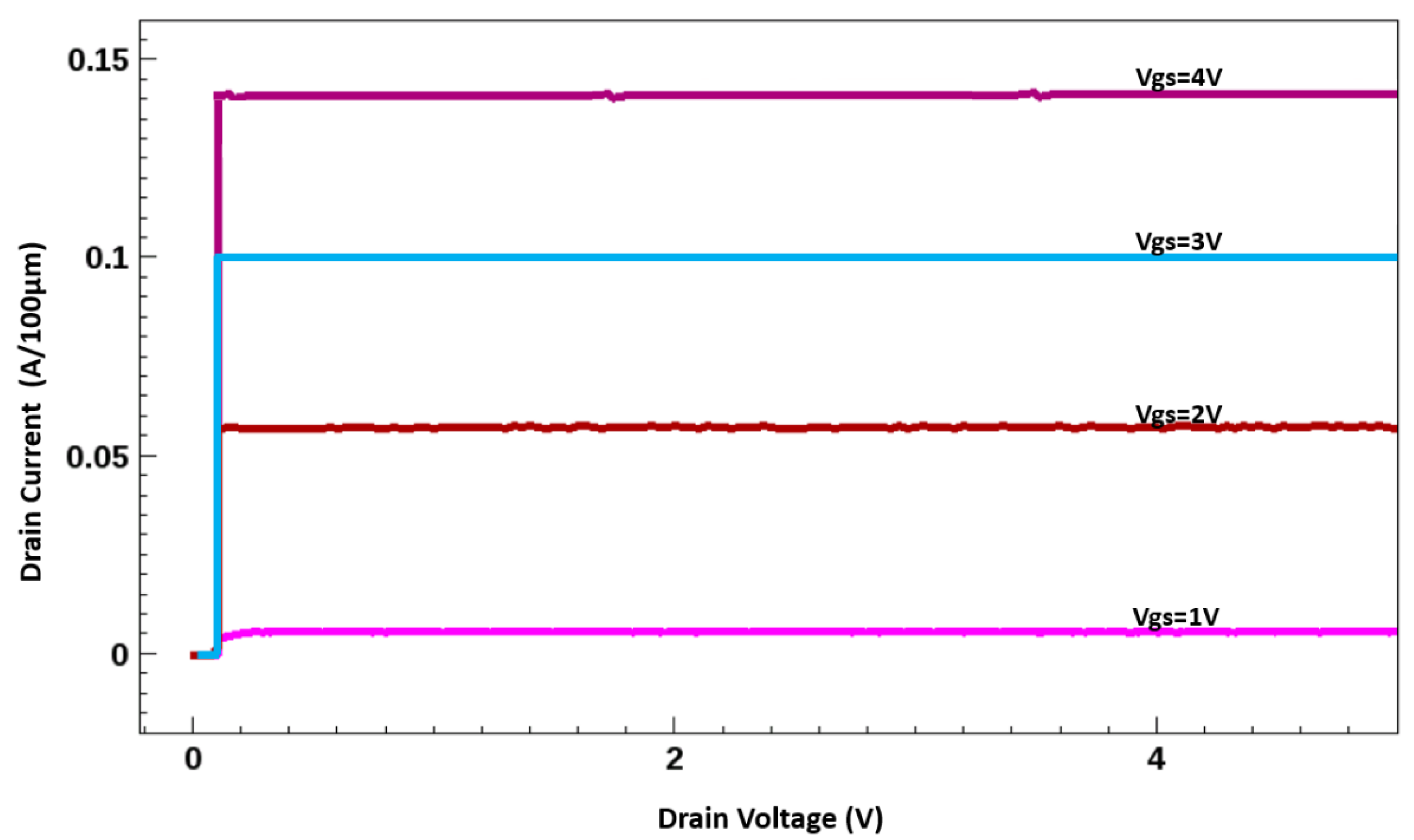
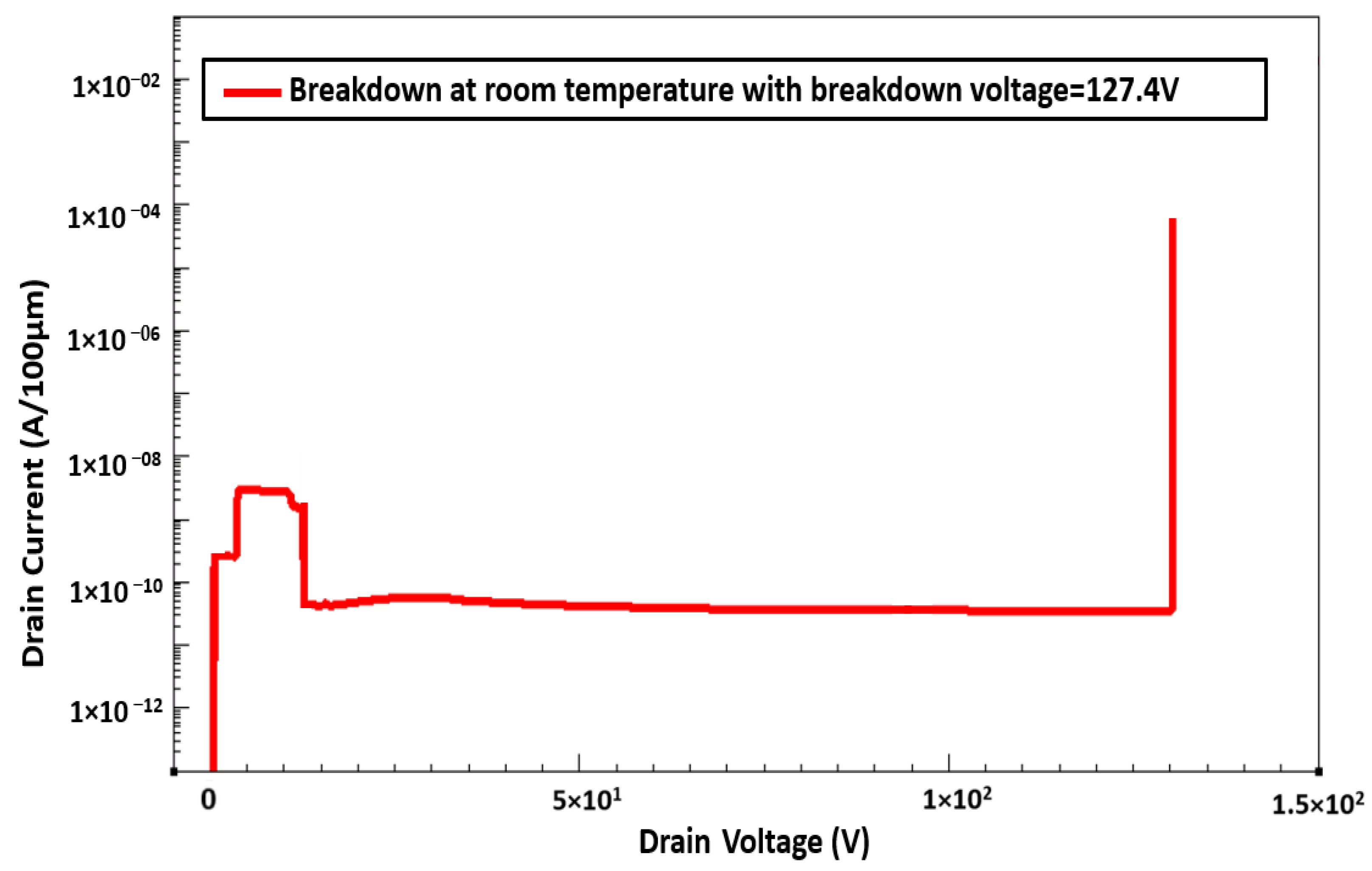
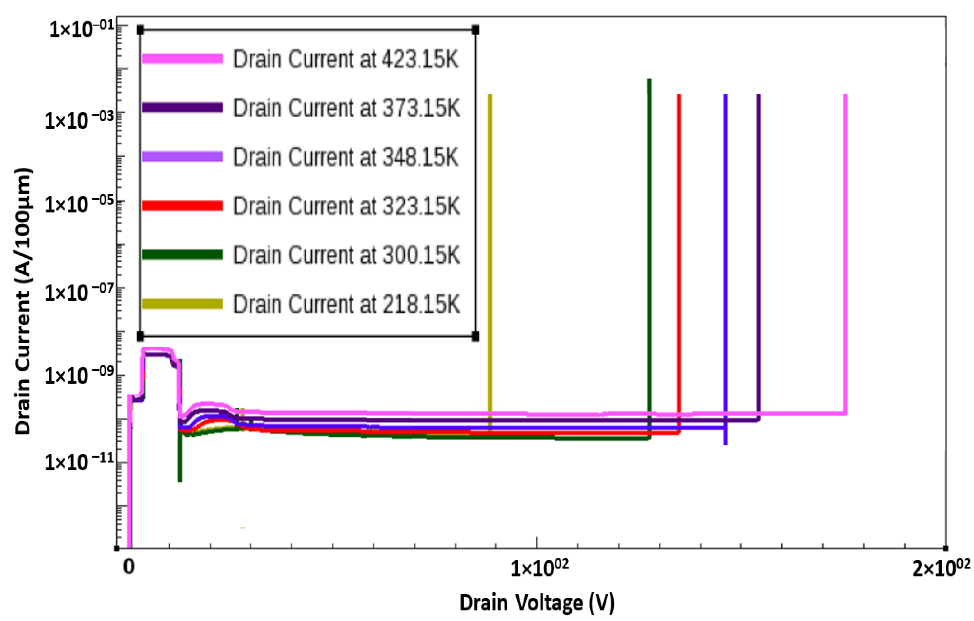
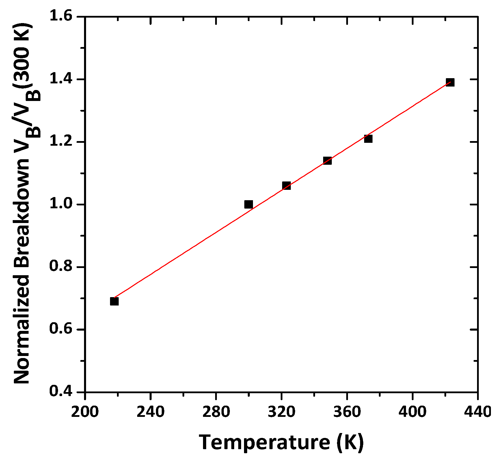
3. Results and Discussion
4. Conclusions
Author Contributions
Funding
Data Availability Statement
Acknowledgments
Conflicts of Interest
References
- Roccaforte, F.; Greco, G.; Fiorenza, P.; Iucolano, F. An overview of normally-off GaN-based high electron mobility transistors. Materials 2019, 12, 1599. [Google Scholar] [CrossRef] [Green Version]
- Ueda, T.; Ishida, M.; Tanaka, T.; Ueda, D. GaN transistors on Si for switching and high-frequency applications. Jpn. J. Appl. Phys. 2014, 53, 100214. [Google Scholar] [CrossRef] [Green Version]
- Hung, T.; Park, P.S.; Krishnamoorthy, S.; Nath, D.N.; Rajan, S. Interface charge engineering for enhancement-mode GaN MISHEMTs. IEEE Electron Device Lett. 2014, 35, 312–314. [Google Scholar] [CrossRef]
- Mishra, U.K.; Shen, L.; Kazior, T.E.; Wu, Y. GaN-based RF power devices and amplifiers. Proc. IEEE 2008, 96, 287–305. [Google Scholar] [CrossRef]
- Sharma, K.; Dasgupta, A.; Ghosh, S.; Ahsan, S.A.; Khandelwal, S.; Chauhan, Y.S. Effect of access region and field plate on capacitance behavior of GaN HEMT. In Proceedings of the 2015 IEEE International Conference on Electron Devices and Solid-State Circuits (EDSSC), Singapore, 1–4 June 2015; pp. 499–502. [Google Scholar]
- Shenai, K.; Chattopadhyay, A. Optimization of High-Voltage Wide Bandgap Semiconductor Power Diodes. IEEE Trans. Electron Devices 2015, 62, 359–365. [Google Scholar] [CrossRef]
- Jones, E.A.; Wang, F.F.; Costinett, D. Review of Commercial GaN Power Devices and GaN-Based Converter Design Challenges. IEEE J. Emerg. Sel. Top. Power Electron. 2016, 4, 707–719. [Google Scholar] [CrossRef]
- Tsurumi, N.; Uemoto, Y.; Sakai, H.; Ueda, T.; Tanaka, T.; Ueda, D. Gan Transistors for Power Switching and High Frequency Applications. In Proceedings of the 2008 IEEE Compound Semiconductor Integrated Circuits Symposium, Monterey, CA, USA, 12–15 October 2008; pp. 1–5. [Google Scholar]
- Palacios, T.; Mishra, U.K. GaN-based transistors for high-frequency applications. Compr. Semicond. Sci. Technol. 2011, 5, 242–298. [Google Scholar]
- Luo, X.; Halder, S.; Curtice, W.R.; Hwang, J.C.; Chabak, K.D.; Walker, D.E.; Dabiran, A.M. Scaling and high-frequency performance of AlN/GaN HEMTs. In Proceedings of the 2011 IEEE International Symposium on Radio-Frequency Integration Technology, Beijing, China, 30 November–2 December 2011; IEEE: Piscataway, NJ, USA, 2011; pp. 209–212. [Google Scholar]
- Jardel, O.; De Groote, F.; Reveyrand, T.; Jacquet, J.-C.; Charbonniaud, C.; Teyssier, J.-P.; Floriot, D.; Quere, R. An Electrothermal Model for AlGaN/GaN Power HEMTs Including Trapping Effects to Improve Large-Signal Simulation Results on High VSWR. IEEE Trans. Microw. Theory Tech. 2007, 55, 2660–2669. [Google Scholar] [CrossRef]
- Raffo, A.; Vadala, V.; Schreurs, D.M.M.-P.; Crupi, G.; Avolio, G.; Caddemi, A.; Vannini, G. Nonlinear Dispersive Modeling of Electron Devices Oriented to GaN Power Amplifier Design. IEEE Trans. Microw. Theory Tech. 2010, 58, 710–718. [Google Scholar] [CrossRef]
- Ding, X.; Zhou, Y.; Cheng, J. A review of gallium nitride power device and its applications in motor drive. CES Trans. Electr. Mach. Syst. 2019, 3, 54–64. [Google Scholar] [CrossRef]
- Amano, H.; Baines, Y.; Beam, E.; Borga, M.; Bouchet, T.; Chalker, P.R.; Charles, M.; Chen, K.J.; Chowdhury, N.; Chu, R.; et al. The 2018 GaN power electronics roadmap. J. Phys. D Appl. Phys. 2018, 51, 163001. [Google Scholar] [CrossRef]
- Geunho, C.; Cha, H.; Kim, H. Parasitic Resistance Effects on Mobility Extraction of Normally-off AlGaN/GaN Gate-recessed MISHFETs. J. Semicond. Technol. Sci. 2018, 2, 78–83. [Google Scholar]
- Chen, K.J.; Yuan, L.; Wang, M.J.; Chen, H.; Huang, S.; Zhou, Q.; Zhou, C.; Li, B.K.; Wang, J.N. Physics of fluorine plasma ion implantation for GaN normally-off HEMT technology. In Proceedings of the 2011 International Electron Devices Meeting, Washington, DC, USA, 5–7 December 2011; IEEE: Piscataway, NJ, USA, 2011. [Google Scholar]
- Liang-Yu, S.; Lee, F.; Huang, J.J. Enhancement-mode GaN-based high-electron mobility transistors on the Si substrate with a P-type GaN cap layer. IEEE Trans. Electron Devices 2014, 61, 460–465. [Google Scholar]
- Greco, G.; Chen, K.J.; Yuan, L.; Wang, M.J.; Chen, H.; Huang, S.; Zhou, Q.; Zhou, C.; Li, B.K.; Wang, J.N. Near-surface processing on AlGaN/GaN heterostructures: A nanoscale electrical and structural characterization. Nanoscale Res. Lett. 2011, 6, 1–7. [Google Scholar] [CrossRef] [PubMed] [Green Version]
- Zhang, Y. Comparison between competing requirements of GaN and SiC family of power switching devices. In Proceedings of the IOP Conference Series: Materials Science and Engineering, Malacca, Malaysia, 6–8 December 2019; No. 1. IOP Publishing: Bristol, VA, USA, 2020; Volume 738. [Google Scholar]
- Lemettinen, J. Epitaxy of Gallium Nitride Films on Silicon Substrates. Master’s Thesis, Aalto University School of Electrical Engineering, Espoo, Finland, 2015. [Google Scholar]
- Song, Y.-L.; Reddy, M.K.; Chang, L.-M.; Sheu, G. Physics-Based TCAD Simulation and Calibration of 600 V GaN/AlGaN/GaN Device Characteristics and Analysis of Interface Traps. Micromachines 2021, 12, 751. [Google Scholar] [CrossRef]
- Reddy, M.K.; Lakshmi, J.; Hemanth, A.; Kumar, B.H.; Bandi, L.; Sheu, G.; Song, Y.-L.; Chen, P.-A.; Chang, L.-M. Physics Based TCAD Simulation and Calibration of GaN/AlGaN/GaN HEMT Device. In Proceedings of the 2019 6th International Conference on Systems and Informatics (ICSAI), Shanghai, China, 2–4 November 2019; pp. 253–256. [Google Scholar]
- Hemanth, A.; Reddy, M.K.; Lakshmi, J.; Kumar, B.H.; Bandi, L.; Sheu, G.; Song, Y.-L.; Chen, P.-A.; Chang, L.-M. Investigations of Low Dynamic Ron on GaN/AlGaN/GaN HEMT by Field Plate Using Physical Device Simulations. In Proceedings of the 2019 6th International Conference on Systems and Informatics (ICSAI), Shanghai, China, 2–4 November 2019; pp. 249–252. [Google Scholar]
- Wu, S.; Richard, T.W.; Anwar, F.M. Physics-based intrinsic model for AlGaN/GaN HEMTs. Mater. Res. Soc. Internet J. Nitride Semicond. Res. 1999, 4, 775–780. [Google Scholar] [CrossRef] [Green Version]
- Miller, D.A.B. Optical physics of quantum wells. In Quantum Dynamics of Simple Systems; Oppo, G.-L., Barnett, S.M., Riis, E., Wilkinson, M., Eds.; Institute of Physics: London, UK, 1996. [Google Scholar]
- Yuan, L.; Wang, M.; Kevin, J.C. Atomistic modeling of fluorine implantation and diffusion in III-nitride semiconductors. In Proceedings of the IEEE International Electron Devices Meeting, San Francisco, CA, USA, 15–17 December 2008; IEEE: Piscataway, NJ, USA, 2008. [Google Scholar]
- Cai, Y.; Cai, Y.; Zhou, Y.; Lau, K.M.; Chen, K.J. Control of threshold voltage of AlGaN/GaN HEMTs by fluoride-based plasma treatment: From depletion mode to enhancement mode. IEEE Trans. Electron Devices 2006, 53, 2207–2215. [Google Scholar] [CrossRef]
- Zaidi, Z.H.; Lee, K.B.; Guiney, I.; Qian, H.; Jiang, S.; Wallis, D.J.; Humphreys, C.J.; Houston, P.A. Enhancement mode operation in AlInN/GaN (MIS) HEMTs on Si substrates using a fluorine implant. Semicond. Sci. Technol. 2015, 30, 105007. [Google Scholar] [CrossRef]
- Ohno, Y.; Ohno, Y.; Nakao, T.; Kishimoto, S.; Maezawa, K.; Mizutani, T. Effects of surface passivation on breakdown of AlGaN/GaN high-electron-mobility transistors. Appl. Phys. Lett. 2004, 84, 2184–2186. [Google Scholar] [CrossRef]
- Kizilyalli, I.C.; Edwards, A.P.; Aktas, O.; Prunty, T.; Bour, D. Vertical power p-n diodes based on bulk GaN. IEEE Trans. Electron Devices 2015, 62, 414–422. [Google Scholar] [CrossRef]
- Cao, L.; Zhu, Z.; Harden, G.; Ye, H.; Wang, J.; Hoffman, A.; Fay, P.J. Temperature Dependence of Electron and Hole Impact Ionization Coefficients in GaN. IEEE Trans. Electron Devices 2021, 68, 1228–1234. [Google Scholar] [CrossRef]


| Physical Phenomenon | Model |
|---|---|
| Mobility | 1a. Doping dependence |
| 1b. High field saturation | |
| 1c. Poole Frankel | |
| Avalanche | 2a. Van overstraeten |
| Recombination | 3a. Shockley-Red-Hall |
| Polarization | 4a. Piezo-Electric Stress |
| 4b. Piezo-Electric Strain | |
| Tunneling | 5a. Electron Barrier Tunneling |
| Self-heating effect | 6a. Thermodynamic |
Publisher’s Note: MDPI stays neutral with regard to jurisdictional claims in published maps and institutional affiliations. |
© 2021 by the authors. Licensee MDPI, Basel, Switzerland. This article is an open access article distributed under the terms and conditions of the Creative Commons Attribution (CC BY) license (https://creativecommons.org/licenses/by/4.0/).
Share and Cite
Sheu, G.; Song, Y.-L.; Susmitha, D.; Issac, K.; Mogarala, R. A Novel Nitrogen Ion Implantation Technique for Turning Thin Film “Normally On” AlGaN/GaN Transistor into “Normally Off” Using TCAD Simulation. Membranes 2021, 11, 899. https://doi.org/10.3390/membranes11110899
Sheu G, Song Y-L, Susmitha D, Issac K, Mogarala R. A Novel Nitrogen Ion Implantation Technique for Turning Thin Film “Normally On” AlGaN/GaN Transistor into “Normally Off” Using TCAD Simulation. Membranes. 2021; 11(11):899. https://doi.org/10.3390/membranes11110899
Chicago/Turabian StyleSheu, Gene, Yu-Lin Song, Dupati Susmitha, Kutagulla Issac, and Ramyasri Mogarala. 2021. "A Novel Nitrogen Ion Implantation Technique for Turning Thin Film “Normally On” AlGaN/GaN Transistor into “Normally Off” Using TCAD Simulation" Membranes 11, no. 11: 899. https://doi.org/10.3390/membranes11110899
APA StyleSheu, G., Song, Y.-L., Susmitha, D., Issac, K., & Mogarala, R. (2021). A Novel Nitrogen Ion Implantation Technique for Turning Thin Film “Normally On” AlGaN/GaN Transistor into “Normally Off” Using TCAD Simulation. Membranes, 11(11), 899. https://doi.org/10.3390/membranes11110899