Topic Editors

Dr. Shoue Chen
School of Packaging, Michigan State University, East Lansing, MI 48824, USA
Lewis Katz School of Medicine, Temple University, Philadelphia, PA 10140, USA
Dr. Ke Xie
Department of Chemistry, Northwestern University, Evanston, IL 60208, USA

Advanced Integrated Circuit Design and Application

Abstract submission deadline
28 February 2026
Manuscript submission deadline
30 April 2026
Viewed by
16666

Topic Information

Dear Colleagues,

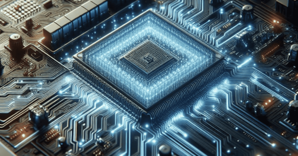
Advanced integrated circuits (ICs) are the keystones of modern electronics, playing a significant role in enabling the development of increasingly powerful, efficient, and versatile electronic devices and systems that renovate our living styles. Among the vast industries and technologies, the application of electronic engineering and IC system design to solve challenges in medical and biological fields has placed this field at the forefront of research and innovation. The potential intersection of biology, medicine, and electrical engineering will have a profound impact on modern healthcare, treatment, and diagnoses of diseases. In addition, owing to the continuous development of smart functional materials and electronics, advanced ICs could be imparted with intelligence and versatile sensory abilities. The ability to build IC systems, especially by combining solid-state electronics with the unique capabilities of bioinspired components, exhibits great promise, along with other innovations in advanced IC designs. The main technical challenges for advanced ICs involve how to construct units with improved performance, lower power consumption, enhanced reliability, smaller footprint, and possibility for new applications. Thus, the developments of emerging IC technologies have been focused on introducing novel device structures, new semiconducting materials, and new architecture to improve performance/integration density and enhance the function of ICs.

We encourage the submissions of original research studies and reviews on novel emerging material technologies—such as zero-dimensional, one-dimensional, two-dimensional, and three-dimensional nanostructured materials; smart and active materials for IC development; flexible thin-film IC designs; IC packaging; smart power ICs; and energy harvesting technologies—and their broad applications in next-generation wearables, health monitoring, as well as touch-sensing and other sensory systems.

Dr. Shoue Chen
Dr. Xiaolong Wang
Dr. Ke Xie
Topic Editors

Keywords

  • transistor
  • semiconductor
  • interface ICs
  • flexible ICs
  • IC packaging
  • nanomaterial
  • bioinspired electronics
  • sensing
  • energy harvesting
  • wearables

Participating Journals

Journal Name Impact Factor CiteScore Launched Year First Decision (median) APC
Electronics
electronics
2.6 5.3 2012 16.4 Days CHF 2400 Submit
Eng
eng
- 2.1 2020 21.5 Days CHF 1200 Submit
Journal of Low Power Electronics and Applications
jlpea
1.6 3.6 2011 20 Days CHF 1800 Submit
Micromachines
micromachines
3.0 5.2 2010 16.2 Days CHF 2100 Submit
Nanomaterials
nanomaterials
4.4 8.5 2010 14.1 Days CHF 2400 Submit

Preprints.org is a multidisciplinary platform offering a preprint service designed to facilitate the early sharing of your research. It supports and empowers your research journey from the very beginning.

MDPI Topics is collaborating with Preprints.org and has established a direct connection between MDPI journals and the platform. Authors are encouraged to take advantage of this opportunity by posting their preprints at Preprints.org prior to publication:

  1. Share your research immediately: disseminate your ideas prior to publication and establish priority for your work.
  2. Safeguard your intellectual contribution: Protect your ideas with a time-stamped preprint that serves as proof of your research timeline.
  3. Boost visibility and impact: Increase the reach and influence of your research by making it accessible to a global audience.
  4. Gain early feedback: Receive valuable input and insights from peers before submitting to a journal.
  5. Ensure broad indexing: Web of Science (Preprint Citation Index), Google Scholar, Crossref, SHARE, PrePubMed, Scilit and Europe PMC.

Published Papers (16 papers)

Order results
Result details
Journals
Select all
Export citation of selected articles as:
17 pages, 869 KiB  
Article
Impact of Mother Wavelet Choice on Fast Wavelet Transform Performances for Integrated ST Segment Monitoring
by Béatrice Guénégo, Caroline Lelandais-Perrault, Emilie Avignon-Meseldzija, Gérard Sou and Philippe Bénabès
J. Low Power Electron. Appl. 2025, 15(2), 31; https://doi.org/10.3390/jlpea15020031 - 12 May 2025
Viewed by 180
Abstract
The ST segment of an ECG signal is a feature that changes in the event of cardiac ischemia, a condition that is an early warning sign of myocardial infarction. Being able to monitor this feature in real time would be highly beneficial for [...] Read more.
The ST segment of an ECG signal is a feature that changes in the event of cardiac ischemia, a condition that is an early warning sign of myocardial infarction. Being able to monitor this feature in real time would be highly beneficial for preventing recurrent heart attacks. However, to be worn daily, such a monitoring device must be extremely miniaturized, down to the scale of a single integrated circuit. Currently, it is possible to integrate a heart rate detector, but, to our knowledge, no existing work presents a chip capable of detecting ST segment deviation. This is mainly because accurate ST segment measurement requires low-distortion signal processing, as specified in the International Electrotechnical Commission (IEC) standard. At the same time, the system is required to filter out baseline wander, whose frequency components may partially overlap with those of the ST segment. In this study, we relied on wavelet-based analysis and reconstruction to compare several wavelet types. We optimized their hyperparameters to minimize implementation complexity while satisfying the low-distortion constraints. We also propose an ASIC-oriented architecture and evaluate its post-layout performance in terms of area and power consumption. The post-layout results indicate that the Daubechies wavelet db3 offers the best trade-off among the evaluated configurations. It exhibits an area utilization of 1.18 mm2 and a post-layout power consumption of 4.89 μW, while preserving the ST segment in compliance with the IEC standard, thanks in particular to its effective baseline wandering filtering of 6.9 dB. These results demonstrate the feasibility of embedding automatic ST segment extraction on-chip. Full article
(This article belongs to the Topic Advanced Integrated Circuit Design and Application)
Show Figures

Figure 1

14 pages, 9820 KiB  
Article
Design and Analysis of an Ultra-Wideband High-Precision Active Phase Shifter in 0.18 μm SiGe BiCMOS Technology
by Hao Jiang, Zenglong Zhao, Nengxu Zhu and Fanyi Meng
J. Low Power Electron. Appl. 2025, 15(2), 30; https://doi.org/10.3390/jlpea15020030 - 7 May 2025
Viewed by 132
Abstract
This paper presents an active phase shifter for phased array system applications, implemented using 0.18 μm SiGe BiCMOS technology. The phase shifter circuit consists of a wideband quadrature signal generator, a vector modulator, an input balun, and an output balun. To enhance the [...] Read more.
This paper presents an active phase shifter for phased array system applications, implemented using 0.18 μm SiGe BiCMOS technology. The phase shifter circuit consists of a wideband quadrature signal generator, a vector modulator, an input balun, and an output balun. To enhance the bandwidth, a polyphase filter is employed as the quadrature signal generator, and a two-stage RC-CR filter with a highly symmetrical miniaturized layout is cascaded to create multiple resonant points, thus extending the phase shifter’s bandwidth to cover the required range. The gain of the variable-gain amplifier within the vector modulator is adjustable by varying the tail current, thereby enlarging the range of selectable points, improving phase-shifting accuracy, and reducing gain fluctuations. The measurement results show that the proposed active phase shifter achieves an RMS phase error of less than 2° and a gain variation ranging from −1.2 dB to 0.1 dB across a 20 GHz to 30 GHz bandwidth at room temperature. The total chip area is 0.4 mm2, with a core area of 0.165 mm2, and consumes 19.5 mW of power from a 2.5 V supply. Full article
(This article belongs to the Topic Advanced Integrated Circuit Design and Application)
Show Figures

Figure 1

12 pages, 6973 KiB  
Article
Investigation on Electromigration-Induced Failure and Reservoir Effect in AlCu Interconnects
by Yuanxiang Zhang, Guoquan Jiang, Jingbo Zhao and Lihua Liang
Micromachines 2025, 16(4), 458; https://doi.org/10.3390/mi16040458 - 13 Apr 2025
Viewed by 298
Abstract
Aluminum–copper alloy (AlCu) is commonly utilized as interconnect material in low-power devices. However, as the size of electronic devices continues to decrease and current density increases, electromigration (EM) has emerged as a significant reliability concern for AlCu interconnects in the microelectronics industry. In [...] Read more.
Aluminum–copper alloy (AlCu) is commonly utilized as interconnect material in low-power devices. However, as the size of electronic devices continues to decrease and current density increases, electromigration (EM) has emerged as a significant reliability concern for AlCu interconnects in the microelectronics industry. In this study, two-level AlCu interconnect structures with a Ti/TiN barrier layer were fabricated using 0.18 μm technology to perform accelerated EM tests. The test samples were subjected to three current levels (1.45 mA, 2.40 mA and 5.30 mA) at three ambient temperatures (200 °C, 225 °C and 250 °C) to investigate the nucleation and evolution of voids during EM degradation and then obtain the mean time to failure (MTTF). The numerical simulation method of atomic density integral (ADI) was used to simulate experimental observations based on the ANSYS platform, considering the coupled effects of electron wind force, stress gradient, temperature gradient, and atomic density gradient. A comparison of the experimental results and numerical simulations proves that the ADI method can be applied successfully to EM failure prediction of AlCu interconnects. Finite element models with different reservoir lengths were built to demonstrate the mechanism of the reservoir effect. The results show that the reservoir can improve the EM lifetime of the interconnect, but there is a critical extension length beyond which increasing extension sizes have no effect on EM lifetime. Full article
(This article belongs to the Topic Advanced Integrated Circuit Design and Application)
Show Figures

Figure 1

24 pages, 6308 KiB  
Article
An Optimized Core Distribution Adaptive Topology Reconfiguration Algorithm for NoC-Based Embedded Systems
by Bowen Hou, Dali Xu, Fangfa Fu, Bing Yang and Na Niu
Micromachines 2025, 16(4), 421; https://doi.org/10.3390/mi16040421 - 31 Mar 2025
Viewed by 370
Abstract
In advanced multicore embedded systems, network-on-chip (NoC) is vital for core communication. With a rise in the number of cores, the incidence of core failures rises, potentially affecting system performance and stability. To address the challenges associated with core failures in network-on-chip (NoC) [...] Read more.
In advanced multicore embedded systems, network-on-chip (NoC) is vital for core communication. With a rise in the number of cores, the incidence of core failures rises, potentially affecting system performance and stability. To address the challenges associated with core failures in network-on-chip (NoC) systems, researchers have proposed numerous topology reconfiguration algorithms. However, these algorithms fail to achieve an optimal balance between topology reconfiguration rate and recovery time. Addressing these issues, we propose an adaptive core distribution optimization topology reconfiguration algorithm, which involves the distribution of faulty cores as the main factor for the reconfiguration procedure. This algorithm is based on a 2D REmesh structure to achieve physical topology reconfiguration, optimized through a bidirectional search algorithm, and features an adaptive algorithm for optimizing core distribution. Experimental results show that a 96.70% successful reconfiguration rate with the proposed algorithm can be guaranteed when faulty cores are less than 68.75% of the max faulty cores. In particular, when the faulty cores reach 8 in the 8 × 9 REmesh, the successful reconfiguration rate is 63.60% with the proposed algorithm, which is 14.80% higher than BTTR and 9.30% higher than BSTR. Additionally, the average recovery time of our algorithm is reduced by 98.60% compared with BTTR and by 15.87% compared with BSTR, significantly improving both the performance and reliability in embedded systems. Full article
(This article belongs to the Topic Advanced Integrated Circuit Design and Application)
Show Figures

Figure 1

14 pages, 1778 KiB  
Article
A 0.81–1.46 ppm/C High-Order Segmented Curvature-Compensation Bandgap Reference with Dynamic Element Matching Offset Cancellation for a Battery Management System
by Jingkai Xu, Wei Wang, Yude Lin, Harikrishnan Ramiah and Xiaochao Li
Electronics 2025, 14(7), 1322; https://doi.org/10.3390/electronics14071322 - 27 Mar 2025
Viewed by 316
Abstract
A precise high-order segmented curvature-compensation bandgap reference (BGR) with dynamic element matching (DEM) offset cancellation has been developed. The proposed segmented curvature-compensation scheme with a resistive trimming network is used to reduce the errors caused by the nonlinear dependence of the bipolar transistor [...] Read more.
A precise high-order segmented curvature-compensation bandgap reference (BGR) with dynamic element matching (DEM) offset cancellation has been developed. The proposed segmented curvature-compensation scheme with a resistive trimming network is used to reduce the errors caused by the nonlinear dependence of the bipolar transistor base-emitter voltage (VBE) on temperature. To decrease the std dev (σ) of the reference voltage (VREF), DEM technology is applied in the core BGR to alleviate the current branch mismatch, as well as the current mirror mismatch in the error amplifier. The proposed BGR circuit is designed on a 0.18 μm BCD process with an active area of 300×375μm and 61.5 μA@5 V current consumption in the bandgap core circuit. The post-simulation results show that the proposed BGR achieves a temperature coefficient (TC) of 0.81–1.46 ppm/°C from −40 °C to 125 °C and a 0.045% σ/μ variation on a 3.2768 V VREF. Full article
(This article belongs to the Topic Advanced Integrated Circuit Design and Application)
Show Figures

Figure 1

14 pages, 679 KiB  
Article
A Multi-Tenant Rate Limiter on FPGA
by Yunfei Guo, Zhichuan Guo and Mengting Zhang
Electronics 2025, 14(6), 1155; https://doi.org/10.3390/electronics14061155 - 15 Mar 2025
Viewed by 366
Abstract
Field-programmable gate arrays (FPGAs) are extensively utilized to accelerate virtualized network functions (VNFs) within cloud networks. Imposing rate limits on different flows can enhance the overall bandwidth utilization of the network. Existing hardware token bucket approaches fundamentally trade off resource efficiency against configuration [...] Read more.
Field-programmable gate arrays (FPGAs) are extensively utilized to accelerate virtualized network functions (VNFs) within cloud networks. Imposing rate limits on different flows can enhance the overall bandwidth utilization of the network. Existing hardware token bucket approaches fundamentally trade off resource efficiency against configuration granularity when supporting massive queues (>512). This paper proposes a novel rate-limiting method based on the token bucket algorithm and achieves efficient resource utilization through head packet scheduling and token-to-time conversion. The experimental results show that our method achieves 1.16% lookup-table (LUT) and 2.62% flip flop (FF) resource usage compared to state-of-the-art methods, while supporting 512 queues with <0.4% rate deviation across a 100 Kbps–10 Gbps range (5-decade dynamic range). Full article
(This article belongs to the Topic Advanced Integrated Circuit Design and Application)
Show Figures

Figure 1

16 pages, 4123 KiB  
Article
High-Precision Time Synchronization Based on Timestamp Mapping in Datacenter Networks
by Lin Li, Baihua Chen, Dexuan Duan and Lei Liu
Electronics 2025, 14(3), 610; https://doi.org/10.3390/electronics14030610 - 4 Feb 2025
Viewed by 1148
Abstract
In datacenter networks, it is necessary to determine whether the path is congested according to the one-way delay of packets. The accurate measurement of one-way delay depends on the high-precision time synchronization of the source device and destination device. We have proposed a [...] Read more.
In datacenter networks, it is necessary to determine whether the path is congested according to the one-way delay of packets. The accurate measurement of one-way delay depends on the high-precision time synchronization of the source device and destination device. We have proposed a time synchronization method based on timestamp mapping, combined with in-band network telemetry technology to obtain the packet send timestamp and receive timestamp on devices. The results show that the maximum synchronization error is 19 ns, and the standard deviation is 7.8 ns with a 100 ms time synchronization period and offset adjustment strategy. The proposed time synchronization method achieves outstanding synchronization accuracy and stability. Full article
(This article belongs to the Topic Advanced Integrated Circuit Design and Application)
Show Figures

Figure 1

19 pages, 553 KiB  
Article
ORNIC: A High-Performance RDMA NIC with Out-of-Order Packet Direct Write Method for Multipath Transmission
by Jiandong Ma, Zhichuan Guo, Yipeng Pan, Mengting Zhang, Zhixiang Zhao, Zezheng Sun and Yiwei Chang
Electronics 2025, 14(1), 88; https://doi.org/10.3390/electronics14010088 - 28 Dec 2024
Viewed by 1369
Abstract
Remote Direct Memory Access (RDMA) technology provides a low-latency, high-bandwidth, and CPU-bypassed method for data transmission between servers. Recent works have proved that multipath transmission, especially packet spraying, can avoid network congestion, achieve load balancing, and improve overall performance in data center networks [...] Read more.
Remote Direct Memory Access (RDMA) technology provides a low-latency, high-bandwidth, and CPU-bypassed method for data transmission between servers. Recent works have proved that multipath transmission, especially packet spraying, can avoid network congestion, achieve load balancing, and improve overall performance in data center networks (DCNs). Multipath transmission can result in out-of-order (OOO) packet delivery. However, existing RDMA transport protocols, such as RDMA over Converged Ethernet version 2 (RoCEv2), are designed for handling sequential packets, limiting their ability to support multipath transmission. To address this issue, in this study, we propose ORNIC, a high-performance RDMA Network Interface Card (NIC) with out-of-order packet direct write method for multipath transmission. ORNIC supports both in-order and out-of-order packet reception. The payload of OOO packets is written directly to user memory without reordering. The write address is embedded in the packets only when necessary. A bitmap is used to check data integrity and detect packet loss. We redesign the bitmap structure into an array of bitmap blocks that support dynamic allocation. Once a bitmap block is full, it is marked and can be freed in advance. We implement ORNIC on a Xilinx U200 FPGA (Field-Programmable Gate Array), which consumes less than 15% of hardware resources. ORNIC can achieve 95 Gbps RDMA throughput, which is nearly 2.5 times that of MP-RDMA. When handling OOO packets, ORNIC’s performance is virtually unaffected, while the performance of Xilinx ERNIC and Mellanox CX-5 drops below 1 Gbps. Moreover, compared with MELO and LEFT, our bitmap has higher performance and lower bitmap block usage. Full article
(This article belongs to the Topic Advanced Integrated Circuit Design and Application)
Show Figures

Figure 1

14 pages, 1207 KiB  
Article
FPGA-Based High-Performance Network Impairment Emulator
by Dexuan Duan, Xinshuo Wang, Lin Li and Lei Liu
Electronics 2024, 13(24), 4998; https://doi.org/10.3390/electronics13244998 - 19 Dec 2024
Viewed by 768
Abstract
With the rapid growth of Wide Area Networks (WANs) and advancements in 5G, cloud computing, and IoT, networks face higher demands for low cost, high capacity, reliability, and security. To ensure these requirements, network impairment emulators have become essential tools for testing and [...] Read more.
With the rapid growth of Wide Area Networks (WANs) and advancements in 5G, cloud computing, and IoT, networks face higher demands for low cost, high capacity, reliability, and security. To ensure these requirements, network impairment emulators have become essential tools for testing and optimizing network performance under various conditions. This paper presents an FPGA-based Network Impairment Emulator (FNIE) that accurately emulates packet loss, reordering, and delay with high throughput and low cost. FNIE can achieve up to 100 Gbps throughput, with a configurable packet loss rate ranging from 0.001% to 100%, with a resolution as fine as 0.001%. It also supports up to 64 descriptor queues for reordering, a maximum reordering extent of 511, and emulates delays from 1 µs to 1 s. Full article
(This article belongs to the Topic Advanced Integrated Circuit Design and Application)
Show Figures

Figure 1

22 pages, 946 KiB  
Article
Design of a Fast and Scalable FPGA-Based Bitmap for RDMA Networks
by Yipeng Pan, Zhichuan Guo and Mengting Zhang
Electronics 2024, 13(24), 4900; https://doi.org/10.3390/electronics13244900 (registering DOI) - 12 Dec 2024
Viewed by 1054
Abstract
Remote direct memory access (RDMA) is widely used within and across data centers due to its low latency, high throughput, and low CPU overhead. To further enhance the transmission performance of RDMA, techniques such as multi-path RDMA have been proposed. However, while these [...] Read more.
Remote direct memory access (RDMA) is widely used within and across data centers due to its low latency, high throughput, and low CPU overhead. To further enhance the transmission performance of RDMA, techniques such as multi-path RDMA have been proposed. However, while these techniques increase throughput, they also introduce significant out-of-order (OoO) packet issues that standard RDMA network interface cards (RNICs) struggle to handle effectively. To address the OoO challenges in RDMA network and ensure the integrity of data, we propose an FPGA-based bitmap which is capable of maintaining high throughput and low latency under OoO conditions. Our design segments the bitmap and maintains status information, achieving the low-latency processing of OoO packets with excellent scalability, thus making it suitable for various network environments. We implement this design on Xilinx AU200 FPGA and test it in a simulated 100 Gbps data center network. The results show that the performance under OoO transmission conditions is comparable to that under in-order conditions, demonstrating the solution’s effectiveness in handling RDMA OoO packets efficiently and ensuring high-performance data transfer in RDMA networks. Full article
(This article belongs to the Topic Advanced Integrated Circuit Design and Application)
Show Figures

Figure 1

17 pages, 834 KiB  
Article
SSPRD: A Shared-Storage-Based Hardware Packet Reordering and Deduplication System for Multipath Transmission in Wide Area Networks
by Jiandong Ma, Zhichuan Guo and Mangu Song
Micromachines 2024, 15(11), 1323; https://doi.org/10.3390/mi15111323 - 30 Oct 2024
Viewed by 956
Abstract
To increase bandwidth and overcome packet loss in Wide Area Networks (WANs), per-packet multipath transmission and redundant transmission are increasingly being used as Software-Defined Wide Area Network (SD-WAN) solutions. However, this results in out-of-order and duplicate packets in the destination network. To restore [...] Read more.
To increase bandwidth and overcome packet loss in Wide Area Networks (WANs), per-packet multipath transmission and redundant transmission are increasingly being used as Software-Defined Wide Area Network (SD-WAN) solutions. However, this results in out-of-order and duplicate packets in the destination network. To restore sequential and unique data streams for multiple connections, hardware packet buffers with significant depth are required due to the large delay difference between WAN paths. To address this issue, SSPRD, a shared-storage-based packet reordering and deduplication system using a Field-Programmable Gate Array (FPGA), is proposed. The storage space for packets and sub-buffers is shared by all sessions with dynamic allocation. Packets are stored in the DDR and are sorted by their descriptors in the buffers. We also develop a sub-buffer-based timeout event handling algorithm. While supporting four sessions, SSPRD achieves a deep reorder buffer on hardware, with a depth of up to 15,360 packets per session. Compared with other solutions, SSPRD reduces buffer space usage by 62.5%, and reaches a packet reordering and deduplicating performance of 10 Gbps for 1500-byte packets. Full article
(This article belongs to the Topic Advanced Integrated Circuit Design and Application)
Show Figures

Figure 1

20 pages, 6342 KiB  
Article
ASIP Performance Enhancement by Hazard Control through Scoreboard
by Xinbing Zhou, Yi Man, Peng Hao, Wei Chen, Bo Yang, Baoguo Ding and Dake Liu
Micromachines 2024, 15(11), 1287; https://doi.org/10.3390/mi15111287 - 23 Oct 2024
Viewed by 1053
Abstract
The application-specific instruction set processor (ASIP) has been gradually accepted in AI, communication, media, game and industry control. The digital signal processor (DSP) is a typical ASIP, whose benefits include high performance in specific domains, low power consumption, high flexibility and low silicon [...] Read more.
The application-specific instruction set processor (ASIP) has been gradually accepted in AI, communication, media, game and industry control. The digital signal processor (DSP) is a typical ASIP, whose benefits include high performance in specific domains, low power consumption, high flexibility and low silicon consumption. One of the challenges for DSP design is to handle problems induced by datapath acceleration. The datapath acceleration (instruction fusion, black box instructions) induces control complexities. To most efficiently utilize hardware, control challenges can be summarized as RAW (Read-After-Write) handling, hardware hazard handling, and WAW (Write-After-Write) handling. Both an advanced compiler and hardware hazard handler can be used as solutions. In this paper, we introduced both solutions and exposed the benefits from the hardware solution. The benefits include utilizing low silicon to achieve higher performance and program memory reduction on chip. In summary, our solution only uses 0.91% extra silicon area yet achieves 32.75% performance improvement. So, the overall performance-to-cost ratio could be evaluated as 32%. Full article
(This article belongs to the Topic Advanced Integrated Circuit Design and Application)
Show Figures

Figure 1

16 pages, 2952 KiB  
Article
A High-Performance FPGA-Based RoCE v2 RDMA Packet Parser and Generator
by Zezheng Sun, Zhichuan Guo, Jiandong Ma and Yipeng Pan
Electronics 2024, 13(20), 4107; https://doi.org/10.3390/electronics13204107 - 18 Oct 2024
Cited by 1 | Viewed by 2191
Abstract
RDMA (Remote Direct Memory Access) technology has been widely applied due to its high-throughput and low-latency characteristics compared with traditional networks. Implementing RDMA with an FPGA (Field-Programmable Gate Array) is a feasible solution. This paper proposes an implementation method for the ROCE v2 [...] Read more.
RDMA (Remote Direct Memory Access) technology has been widely applied due to its high-throughput and low-latency characteristics compared with traditional networks. Implementing RDMA with an FPGA (Field-Programmable Gate Array) is a feasible solution. This paper proposes an implementation method for the ROCE v2 (Remote Direct Memory Access) protocol packet parser and generator based on an FPGA, capable of supporting various transaction packet types, such as RDMA READ, RDMA WRITE, and SEND, under the Reliable Connection service. The RDMA READ and RDMA WRITE performance of RDMA is close to 100 Gbps, which provides a feasible solution for the application of wide-area networks. Full article
(This article belongs to the Topic Advanced Integrated Circuit Design and Application)
Show Figures

Figure 1

16 pages, 5753 KiB  
Article
Picowatt Dual-Output Voltage Reference Based on Leakage Current Compensation and Diode-Connected Voltage Divider
by Yuying Huang, Yanshen Luo and Yanhan Zeng
Electronics 2024, 13(17), 3533; https://doi.org/10.3390/electronics13173533 - 5 Sep 2024
Cited by 2 | Viewed by 1403
Abstract
A picowatt CMOS voltage reference with dual outputs is proposed and simulated in this paper based on a standard 65 nm process. To compensate for the leakage current caused by parasitic reverse-biased PN junctions, an approach employing gate leakage transistors is proposed. Maintaining [...] Read more.
A picowatt CMOS voltage reference with dual outputs is proposed and simulated in this paper based on a standard 65 nm process. To compensate for the leakage current caused by parasitic reverse-biased PN junctions, an approach employing gate leakage transistors is proposed. Maintaining a maximal temperature coefficient (TC) of 20.40 ppm/°C across an extended temperature range of −10∼155 °C is achieved. Additionally, a voltage divider consisting of diode-connected NMOS transistors is introduced to obtain a lower voltage output without shunting the original branch or utilizing operational amplifiers. Moreover, a novel trimming block is utilized to optimize TC across different process corners. Simulation results demonstrate that a minimum power consumption of only 53.83 pW is achieved and the line sensitivity is 0.077%/V with 0.45 V to 2.5 V supply. The power supply rejection ratio of −76.70 dB at 10 Hz and VDD = 1.8 V is obtained. Full article
(This article belongs to the Topic Advanced Integrated Circuit Design and Application)
Show Figures

Figure 1

14 pages, 2171 KiB  
Article
An Ultra-Low-Voltage Transconductance Stable and Enhanced OTA for ECG Signal Processing
by Yue Yin, Xinbing Zhang, Ziting Feng, Haobo Qi, Haodong Lu, Jiayu He, Chaoqi Jin and Yihao Luo
Micromachines 2024, 15(9), 1108; https://doi.org/10.3390/mi15091108 - 30 Aug 2024
Cited by 2 | Viewed by 1328
Abstract
In this paper, a rail-to-rail transconductance stable and enhanced ultra-low-voltage operational transconductance amplifier (OTA) is proposed for electrocardiogram (ECG) signal processing. The variation regularity of the bulk transconductance of pMOS and nMOS transistors and the cancellation mechanism of two types of transconductance variations [...] Read more.
In this paper, a rail-to-rail transconductance stable and enhanced ultra-low-voltage operational transconductance amplifier (OTA) is proposed for electrocardiogram (ECG) signal processing. The variation regularity of the bulk transconductance of pMOS and nMOS transistors and the cancellation mechanism of two types of transconductance variations are revealed. On this basis, a transconductance stabilization and enhancement technique is proposed. By using the “current-reused and transconductance-boosted complementary bulk-driven pseudo-differential pairs” structure, the bulk-driven pseudo-differential pair during the input common-mode range (ICMR) is stabilized and enhanced. The proposed OTA based on this technology is simulated using the TSMC 0.18 μm process in a Cadence environment. The proposed OTA consumes a power below 30 nW at a 0.4 V voltage supply with a DC gain of 54.9 dB and a gain-bandwidth product (GBW) of 14.4 kHz under a 15 pF capacitance load. The OTA has a high small signal figure-of-merit (FoM) of 7410 and excellent common-mode voltage (VCM) stability, with a transconductance variation of about 1.35%. Based on a current-scaling version of the proposed OTA, an OTA-C low-pass filter (LPF) for ECG signal processing with VCM stability is built and simulated. With a −3 dB bandwidth of 250 Hz and a power consumption of 20.23 nW, the filter achieves a FoM of 3.41 × 10⁻¹³, demonstrating good performance. Full article
(This article belongs to the Topic Advanced Integrated Circuit Design and Application)
Show Figures

Figure 1

17 pages, 2338 KiB  
Article
Energy-Efficient Neural Network Acceleration Using Most Significant Bit-Guided Approximate Multiplier
by Pengfei Huang, Bin Gong, Ke Chen and Chenghua Wang
Electronics 2024, 13(15), 3034; https://doi.org/10.3390/electronics13153034 - 1 Aug 2024
Viewed by 1429
Abstract
The escalating computational demands of deep learning and large-scale models have led to a significant increase in energy consumption, highlighting the urgent need for more energy-efficient hardware designs. This study presents a novel weight approximation strategy specifically designed for quantized neural networks (NNs), [...] Read more.
The escalating computational demands of deep learning and large-scale models have led to a significant increase in energy consumption, highlighting the urgent need for more energy-efficient hardware designs. This study presents a novel weight approximation strategy specifically designed for quantized neural networks (NNs), resulting in the development of an efficient approximate multiplier leveraging most significant one (MSO) shifting. Compared to both energy-efficient logarithmic approximate multipliers and accuracy-prioritized non-logarithmic approximate multipliers, our proposed logarithmic-like design achieves an unparalleled balance between accuracy and hardware costs. When compared with the baseline exact multiplier, our innovative design exhibits remarkable reductions, encompassing a decrease of up to 28.31% in area, a notable 57.84% reduction in power consumption, and a diminution of 11.86% in delay. Experimental outcomes reveal that the proposed multiplier, when applied in neural networks, can conserve approximately 60% of energy without compromising task accuracy. Concurrently, experiments focused on the transformer accelerator and image processing illustrate the substantial energy savings that can be obtained for Large Language Models (LLMs) and image processing tasks through the implementation of our proposed design, further validating its efficacy and practicality. Full article
(This article belongs to the Topic Advanced Integrated Circuit Design and Application)
Show Figures

Figure 1

Back to TopTop