2.1. ROIC Design
The AFE is a mixed-signal circuit mainly composed of ROIC and TS-SS ADC. The ROIC includes a 64 × 64 pixel array, a column-level circuit, an output buffer, and a bias circuit. The TS-SS ADC comprises a sampling and hold circuit, comparator, latch, ramp generator, and digital circuits. The overall structure is shown in
Figure 2. The analog signal chain needs to ensure adequate linearity and output dynamic range. The digital circuit provides timing control to achieve coordinated operation of the AFE.
In a global shutter, since all pixels are exposed at the same time, the integrated voltage needs to be held on the holding capacitor after exposure is completed. In the readout stage, due to the fact that pixels with lower readout order need to maintain the integrated voltage for a long period of time, there may be a leakage problem with the holding capacitor during the readout stage, which results in a deviation of the integrated voltage. In order to mitigate this impact, a rolling shutter and array partitioning technology are adopted to shorten the holding time from 10 ms per frame to 320 µs, greatly reducing the impact of leakage. Therefore, we divide a 64 × 64 array into four 32 × 32 sub-arrays.
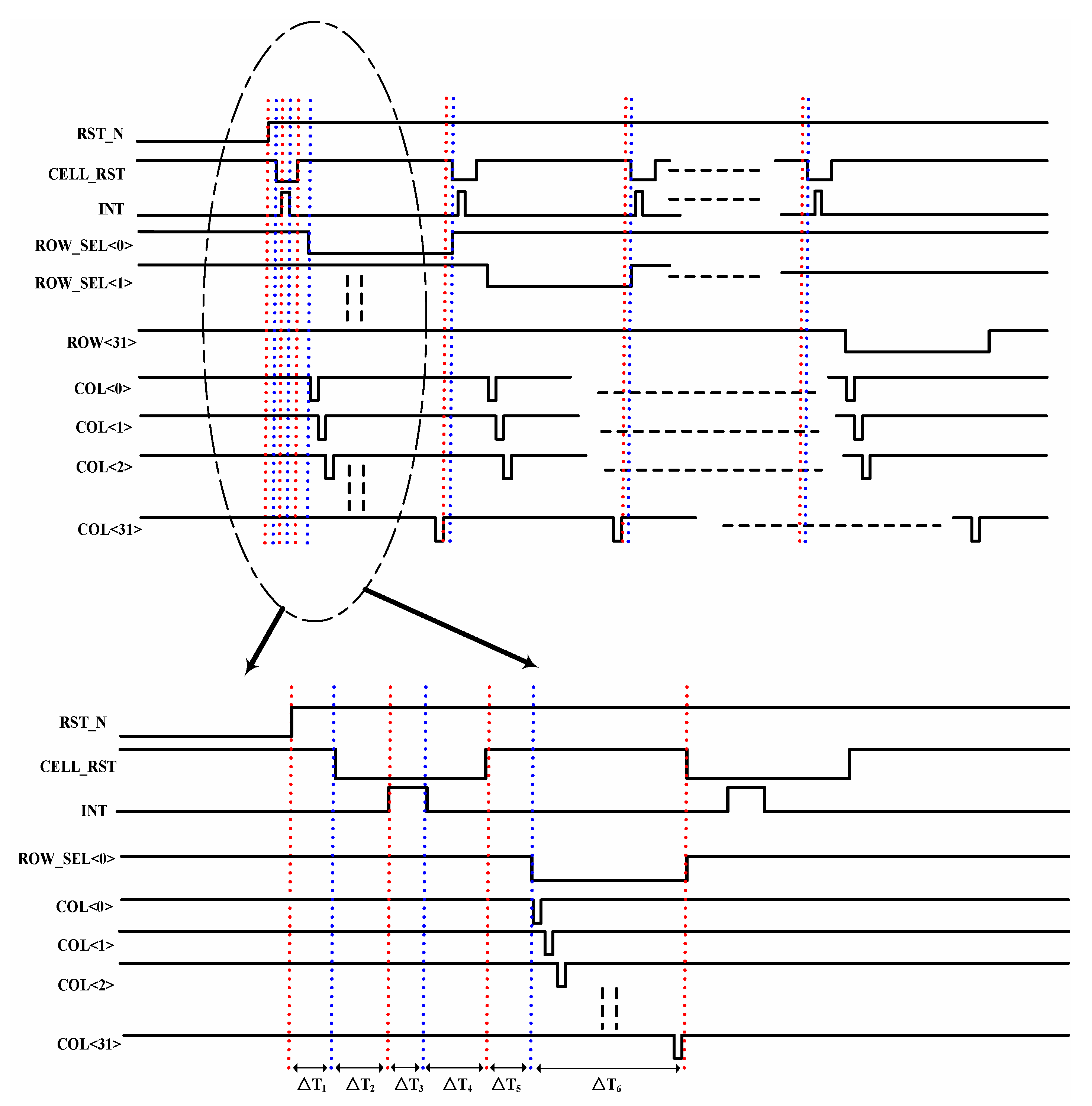
The timing diagram of the ROIC is illustrated in
Figure 3. The input signals include the clock (CLK) and the global reset (RST_N), while the output signals comprise the cell reset (CELL-RST), integration (INT), row selection (ROW<0:31>), and column selection (COL<0:31>) signals.
As shown, the values of ΔT1, ΔT2, ΔT4, and ΔT5 are consistent, with each representing a non-overlapping period of one clock cycle. ΔT3 denotes the integration time, and ΔT6 corresponds to the row readout time. Within each row’s readout time (ΔT6), all columns are read out sequentially.
The operational sequence for each pixel row involves reset, integration, and readout, with the reset-integration time interval separating consecutive rows. The process begins when RST_N is asserted low, which pulls INT low and sets all other output signals high. During the reset phase, CELL-RST is pulled low one clock cycle after RST_N returns high to reset the row. Following another clock cycle, INT goes high, initiating the integration operation. Upon completion of integration, CELL-RST is pulled high after one clock cycle to prevent premature signal reset before readout. The readout stage commences one clock cycle later: CELL-RST remains high as row selection signals ROW<0:31> are enabled sequentially, each lasting for 320μs. During each row selection period, column selection signals COL<0:31> are activated in sequence, with each lasting for 10μs to complete data readout.
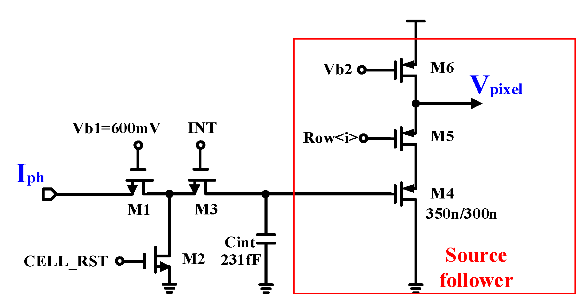
Pixel circuits need to compromise performance parameters such as injection efficiency, layout area, and noise. In this paper, a DI structure is chosen as the pixel circuit for the ROIC. DI can be applied in a small pixel while ensuring high linearity and dynamic range. Its basic structure is shown in
Figure 4. Its operation principle is as follows: when transistor M2 is turned off and M3 is turned on, integration begins. After integration is complete, M2 is turned on and M3 is turned off, providing a circuit for photocurrent to prevent charge accumulation from causing changes in the switch state. M4, M5, and M6 form a dynamic power source follower, which isolates the pixel from the column bus and prevents interference on the column bus from affecting the integration voltage. Among them, M4 is the amplification transistor and M5 is the switch transistor. During the readout phase, when the row selection signal COL_SEL (Vrow) is active, M5 conducts and the source follower transmits the integrated voltage to the source of M5, while also conducting M2 to discharge the photocurrent from M2 to the ground. This scheme avoids any impact on surrounding cells. During the integration process, M5 is disconnected, and the pixel output is reset to VDD.
Given the relatively small current range of 7 nA to 100 nA, the injection transistor can be appropriately biased in the subthreshold region. When M1 operates in the subthreshold region, its current is related to the gate-source voltage as follows:
From the above equation, it can be seen that the leakage current is independent of the drain-source voltage. The drain-source voltage of the injection transistor should be greater than 0.1 V to ensure stability of the detector. Cint is an integration capacitor. For the selected process in this paper, the unit area capacitance value of the MOS capacitor is 4.97 fF/μm2, while the unit area capacitance value of the MIM capacitor is 2 fF/μm2. Therefore, the MOS capacitor is more suitable for the design. Considering all factors, the PMOS capacitor is adopted. MOS devices used as capacitors need to consider their operating regions, namely the inversion region and the accumulation region. When operating in the inversion region, the MOS capacitance is unstable, and this region should be avoided during pixel integration to avoid serious nonlinear errors.
Due to the manufacturing mismatches, there will be a certain deviation in the threshold voltage of each MOS transistor, which can cause output deviation under the same input or in the absence of light, and this deviation is defined as fixed pattern noise (FPN) [
11]. The impact of this noise on the overall performance is significant, and it is also the largest contributing factor to noise in ROIC. It can be reduced through correlated double-sampling (CDS) techniques [
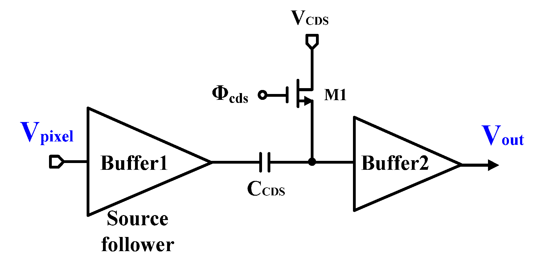
12]. A passive CDS circuit is used as shown in
Figure 5. Buffer1 is the source follower in the DI structure. The left plate of
CCDS samples the reset voltage
VRST when the Φ
CDS is active and M1 is on, and the voltage on the right plate of
CCDS is
VCDS. At this time, the charge on the capacitor can be expressed as
After the pixel integration is completed, the Φ
CDS becomes invalid, the switch S1 is turned off, and the left plate of
CCDS samples
Vpixel. At this time, the charge on
CCDS is
The following can be obtained from the conservation of charge:
Vpixel and
VRST are the pixel integration voltage and reset voltage, respectively. This circuit uses only one capacitor to achieve the function of correlated double-sampling, which is suitable for column-level readout circuits and can also be designed inside the pixel if the area allows [
13].
The passive CDS is dimensioned. Meanwhile, its clamp-to-sample timing is chosen to suppress reset/FPN and low-frequency components while keeping the column chain compact.
Figure 5.
Passive CDS circuit.
Figure 5.
Passive CDS circuit.
Although this circuit has the advantages of a small area and low power consumption, CCDS will redistribute charges with the junction capacitor of M1 and the input capacitor of Buffer2. Therefore, CCDS must be large enough; otherwise, the parasitic capacitor will seriously affect the output swing.
2.2. 12 Bit/100 kHz TS-SS ADC
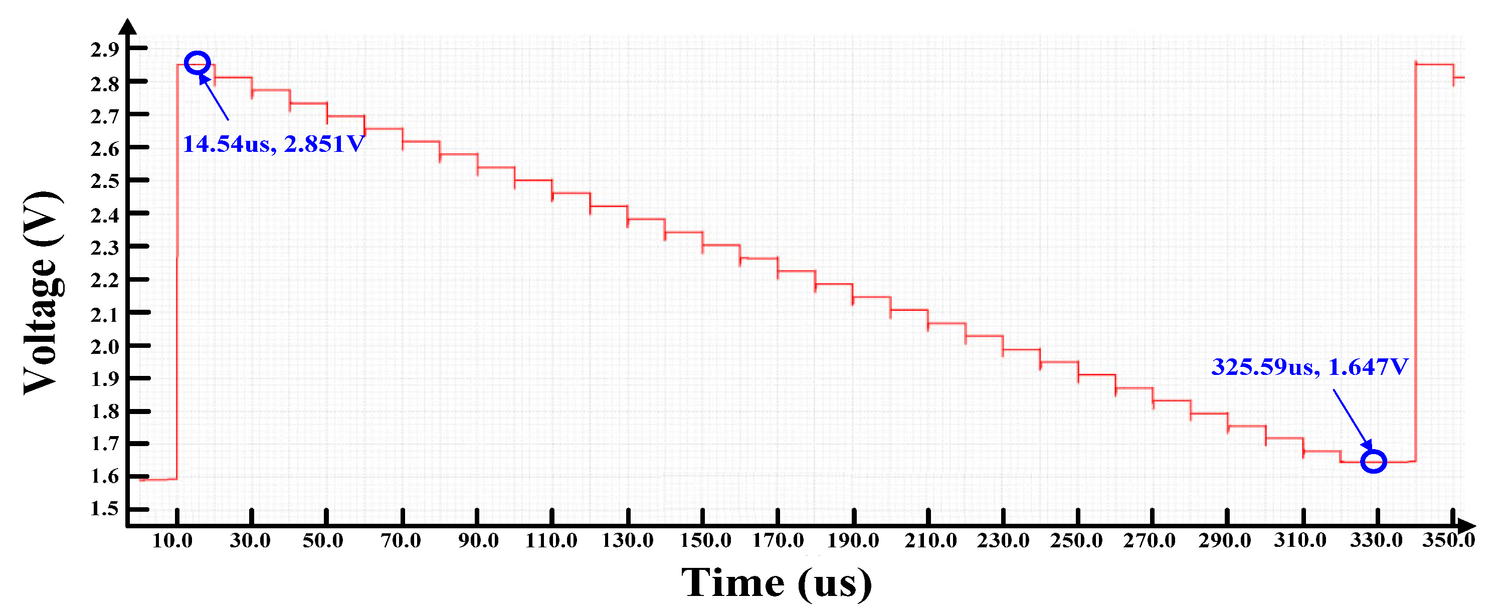
Figure 6 shows the structure of the TS-SS ADC, which mainly includes a sampling and hold circuit, a comparator, a coarse ramp generator, a fine ramp generator, a current-steering DAC, and a digital module. The storage capacitor
CH is not connected across the coarse ramp generator and the fine ramp generator, but is directly connected to the ground.
The quantization of ADC is accomplished based on the counter. The ramp generator generates a voltage reference for the comparator according to the output of the counter. Therefore, the performance of the counter also affects the establishment time of the ramp signal, etc. According to the different clock control methods, counters can be classified into synchronous and asynchronous counters. In an asynchronous counter, the delay time of each flip-flop is Td, meaning that the delay time of the last flip-flop is nTd. In a synchronous counter, each trigger is controlled by the master clock, so its delay time is Td. To achieve the minimum delay time, the synchronous counter is adopted in this paper.
The ramp generator adopts a voltage divider structure. The output of the counter cannot be directly applied to the on–off switch and needs to be decoded by a decoder. The binary code counting method is adopted. For a 6-bit decoder, when the value of the counter is 000000, only switch S0 is on. When the value of the counter is 000001, only switch S1 is on, and so on.
Since the design of the decoder does not require very high driving capacity, this paper adopts a 6-input NAND to save area and reduce power consumption.
In the sampling phase, the switch
SC is closed, and the sampling and hold circuit samples the output voltage of the ROIC, and the voltage is sampled to the inverting input terminal of the four-input comparator. The switch
SH is turned on, and
Vref inputs to one positive and one negative input terminal. Therefore, the input of the comparator can be expressed as
VS is the common-mode voltage output by the sampling and hold circuit, which is the lowest level of the coarse ramp generator.
In the coarse quantization stage,
SC and
SF remain closed, and counting begins after the coarse quantization counter is reset. The voltage of each step in the coarse ramp generator is
VC[
i], and the input of the comparator at this time is
When Δ
Vin > 0, the output of the comparator flips, and the latch uses an edge-triggered structure. The rising edge of the comparator triggers the operation of the latch, and the value of the counter is latched as the result of coarse quantization. Switch
SC is disconnected, and the voltage on the storage capacitor is
ΔV is the voltage of each step of the resistor array.
In the fine quantization stage, the edges of the quantization interval may cause errors in comparator results, resulting in a quantization dead zone. Therefore, the accuracy of the fine ramp generator is 7 bits instead of 6 bits, and its quantization range is 2Δ
V. The lowest and highest voltage of the ramp are
The counter undergoes a reset process to ensure that the initial voltage of the fine ramp generator is
VL. After the reset is complete, the 7-bit fine quantization counter starts counting, causing the ramp voltage to rise accordingly. Switch
SH is turned off, and
SF is turned on. Then the count value
i controls the decoder. The output of the decoder controls the switching of the resistor array to generate a fine ramp voltage. At this time, the differential input of the comparator is
And the output voltage of the fine ramp generator is
Equation (10) can be simplified as
As the value of the counter increases, the input of the comparator gradually increases. When Vin > 0, the comparator flips to high, and the latch also uses an edge-triggered structure. The rising edge of the comparator triggers the latch to operate, and the value of the counter is latched as the result of fine quantization. The results of fine and coarse quantization are added to obtain D[0:11]. Due to the addition of a quantization redundancy bit in the fine quantization stage to prevent dead zones, the output code will be 32 more than the ideal value. Therefore, it is necessary to subtract D[0:11] from 000000 100,000 to obtain the correct result Dout [11:0]. At this point, the 12-bit TS-SS ADC quantization is completed.
The 7-bit (2ΔV) fine ramp acts as a redundancy window around the coarse–fine boundary, eliminating dead zones and relaxing comparator settling; connecting CH to ground avoids cross-domain charge sharing between the coarse and fine ramps.
The dynamic comparator is shown in
Figure 7, consisting of a dynamic latch, two-stage preamplifiers, and an output buffer.
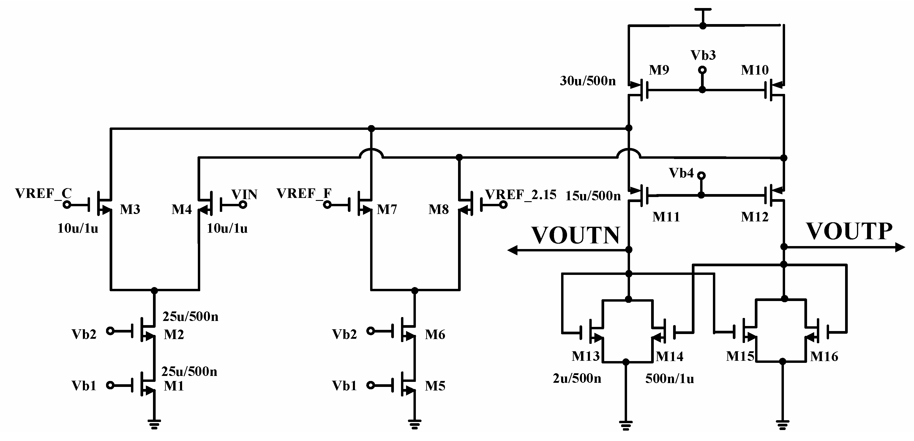
Under the selected process, the threshold voltage of MOS is about 0.75 V (power supply voltage is 3.3 V), and the maximum common-mode input signal can only reach 2.55 V, while the maximum output voltage of ROIC is 3 V. In order to meet the requirements of the input swing, the first preamplifier adopts a folded structure. Due to its input-stage topology, the folded amplifier can effectively expand the input common-mode range, making it more advantageous than ordinary operational amplifiers, especially in low-voltage and high-performance designs. At the same time, the input differential transistor is divided into two pairs, and the common mode range can reach 2.55 V. The cascode current mirror improves the common-mode rejection ratio and enhances the stability of the tail current, as shown in
Figure 8. The structure of the second preamplifier is similar to that of the first stage, except it uses a fully differential structure with two inputs.
The schematic of the comparator is shown in
Figure 9. Compared to the Strong-Arm comparator, the proposed comparator features lower input kickback noise and power consumption.
When CLK is low, the dynamic latch is in the reset phase. M8 and M9 are turned on, and both VOUTP and VOUTN are reset to VDD. M1 is turned off, so there is no current path from VDD to ground. Energy consumption during this process occurs only when VDD charges the output capacitance.
When CLK is high, the dynamic comparator enters the comparison phase. M8 and M9 are turned off. The input voltages VIN and VIP determine the current flowing through M2 and M3. When VIN > VIP, the current of M2 is greater than that of M3, which means the source potential of M4 drops faster than that of M5. The voltage difference between them is amplified by the positive feedback of the latch. Finally, VOUTP is pulled to VDD and VOUTN is pulled to GND, completing the comparison. When VIN < VIP, the current of M2 is less than that of M3. The voltage difference at their source terminals is amplified by the positive feedback of the latch. Finally, VOUTP becomes GND and VOUTN becomes VDD.
From the above analysis, it can be seen that the gain of the dynamic latch varies with time. The expression is as follows:
The expression for the time constant
τ is
where
gm is the transconductance of the inverter, and
CL is the load of the dynamic latch. The 12-bit ADC requires the comparison accuracy to reach LSB/2, and the delay time is half of the clock cycle, T/2. Therefore, we have the following:
Thus, we obtain the transconductance of the inverter:
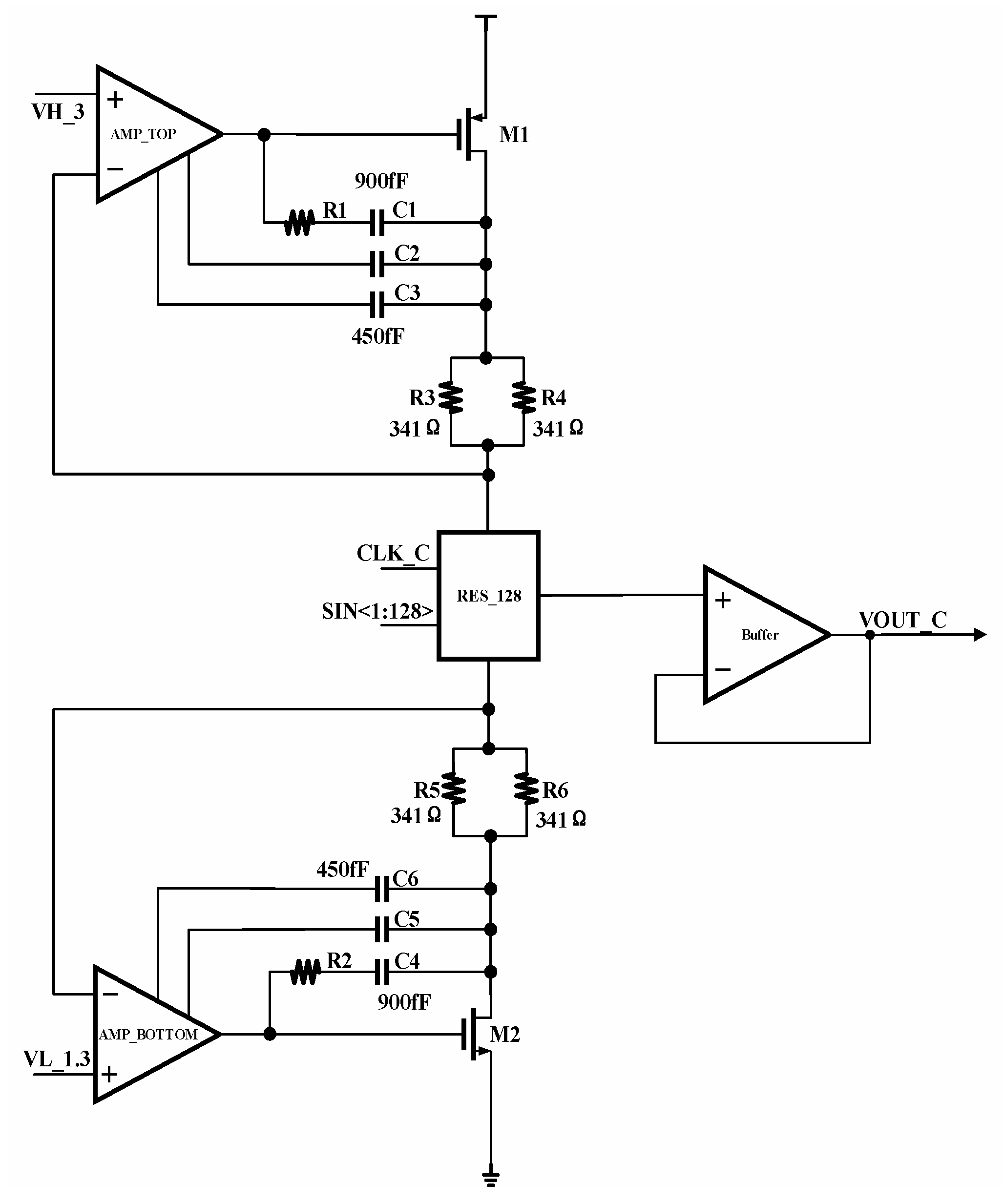
The structure of the ramp generator is shown in
Figure 10, which mainly includes two clamp op-amps, a resistor array, a counter, a decoder, and an output buffer. The top clamp op-amp (AMP TOP) clamps the top potential of the resistor array to 3 V through negative feedback, and the bottom clamp op-amp (AMP BOTTOM) clamps the bottom potential of the resistor array to 1.3 V through negative feedback. The output of the counter controls the decoder, and each bit of the decoder effectively outputs the voltage of the resistor array in sequence. The output buffer is designed to enhance the driving capability by isolating the ramp generator from the next circuit.
The top clamp op-amp of the ramp generator is a two-stage op-amp. The first stage uses a folded cascode amplifier with NMOS input due to the high common-mode level. The second stage uses a Class AB output stage, as shown in
Figure 11. Correspondingly, due to the low common-mode level of the bottom clamp op-amp input, its first stage is a folded-cascode amplifier with PMOS input.
At the end of coarse quantization, the charges in the channel will flow into
CH due to the influence of charge injection, resulting in deviation during the fine quantization process and affecting the quantization accuracy. A current-steering digital-to-analog converter (DAC) is used to correct this deviation. The amount of charge injected into capacitor
CH by switch
SC is
δ is the charge injection coefficient; therefore, the voltage change caused by
Q on
CH is
It can be seen that Δ
VCH is related to m, and the derivative of m can be obtained
According to Equation (17), the variation of Δ
VCH is a linear relationship that can be eliminated by DAC. After considering the error caused by
SC, Equation (10) becomes
VDAC(
m) is the output of DAC, and its voltage value can be designed to be equal to
Vref + Δ
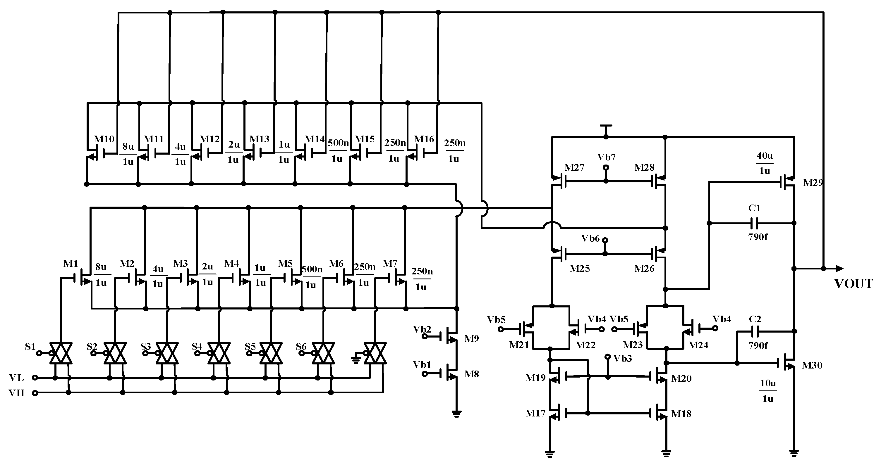
VCH to eliminate the influence of charge injection. Due to the low performance requirements of the calibrated DAC, a current-steering DAC can meet the system requirements, as shown in
Figure 12.
During ramp operation, the current-steering path is used to compensate code-dependent switch injection and static element mismatch, stabilizing the INL/DNL presented to the TS-SS conversion.
The current-steering DAC consists of a two-stage operational amplifier. The MOSFETs at the non-inverting input are composed of M1 to M7, while the MOSFETs at the inverting input are composed of M10 to M16. The sizes of M1 to M6 and M10 to M15 increase in binary-weighted proportions. When the operational amplifier is configured in a unity-gain feedback structure, the analog output voltage can be adjusted by controlling switches S1 to S6. Its output is as follows:
VL is the lowest output voltage,
VH is the highest output voltage,
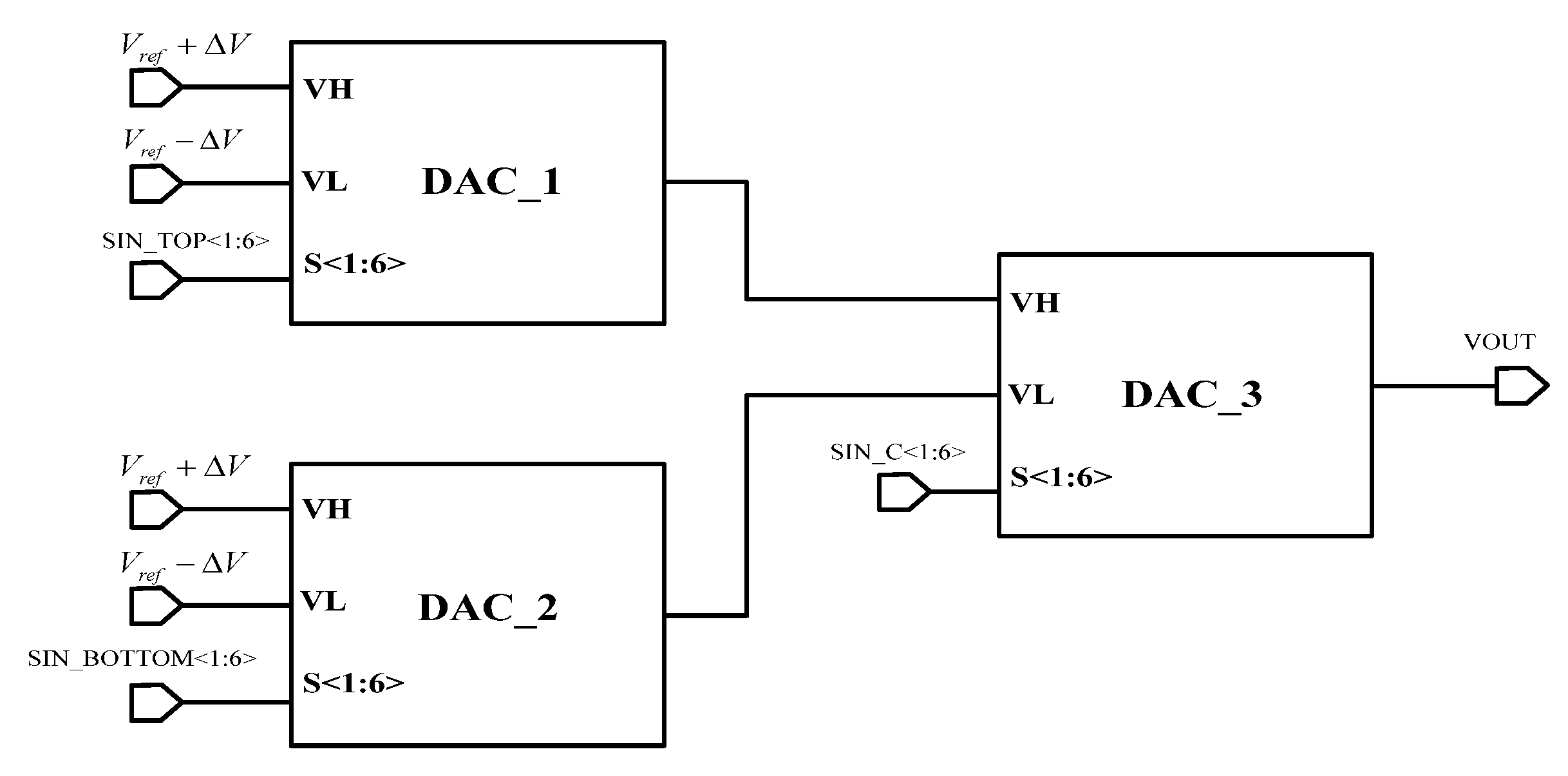
N is the number of bits in the DAC, and D is the decimal value corresponding to the input binary code. By combining Equations (20) and (21), it can be concluded that it is difficult to eliminate the error caused by the charge injection of switch Sc using a single DAC. Therefore, this paper employs three identical DACs connected in series to mitigate the effects of charge injection as shown in
Figure 13. The outputs of DAC_1 and DAC_2 are connected to the
VH and
VL inputs of DAC_3, respectively, while the input of DAC_3 is driven by the value of the coarse quantization counter.
DTOP is the input digital code of DAC_1, and Equation (22) can be simplified as
Similarly, the output of DAC_2 is
Therefore, the total output
VOUT can be expressed as
Because VDAC(m) = Vref + ΔVCH, when the second term of Equation (25) is equal to ΔVCH, the purpose of calibration can be achieved. Since DTOP = DBOTTOM = 100,000, VOUT defaults to output Vref.
Recent works report static-linearity improvements for current-steering DACs by (i) order-statistics/optimal-arrangement (OA) of unary MSB elements after foreground characterization (building a code-mapping LUT at start-up) [
14,
15], and (ii) split-DAC, comparator-based background calibration that generates a binary error (sign-LMS) to track slow PVT drift [
16]. While our prototype keeps the baseline ramp DAC unchanged, these techniques are compatible with the present TS-SS architecture and could be added as non-intrusive options in future revisions for further INL/DNL reduction.
