1. Introduction
High-voltage and high-precision operational amplifiers (OPAs) play a crucial role in applications such as industrial sensor interfaces, high-side current sensing, power-line monitoring, and automotive diagnostics. These systems often require a wide input, common-mode voltage range that spans from ground to the full supply voltage. Therefore, it is important for OPAs to operate reliably under a power supply voltage of 5–55 V while supporting input voltage swing from 0 V up to 55 V. To meet these requirements, a rail-to-rail differential input stage is typically adopted, which enables full-range common-mode signal acquisition without compromising noise and offset performance. In order to extract weak sensor signals, these OPAs need to have low offset and low noise characteristics. The auto-zero and chopper techniques are two main methods for reducing DC offset and low-frequency noise, collectively known as dynamic offset compensation techniques. These two technologies can not only suppress DC offset voltage (current), but also reduce the drift of offset in temperature and time [
1,
2,
3,
4,
5,
6]. Auto-zero is a time-domain modulation method that performs sampling and subtraction operations on the offset and input signal in two phases of one clock cycle; chopper is a frequency-domain modulation method that modulates the input signal and offset to different frequencies, and then filters the offset. Due to the fact that low-frequency noise is very close in frequency to DC offset signals, dynamic offset compensation techniques cannot distinguish between low-frequency noise and offset to a certain extent. Therefore, auto-zero and chopper will also process low-frequency noise efficiently [
7].
Auto-zero and chopper have their own advantages in dealing with low-frequency noise and offset, but there are also some shortcomings. Although auto-zero can reduce the in-band offset, the noise spectrum folding and the offset sampling operation related can lead to an increase in the power spectral density (PSD) of in-band noise. A well-designed chopper OPA can have an extremely low in-band noise PSD, with its level almost the same as its original thermal noise PSD. In chopper OPAs, the two most important non-ideal characteristics are high-frequency ripple and glitch caused by modulation and charge injection. Ripple occurs at the odd harmonic frequencies of chopper frequency, while glitch appears at the even harmonic frequencies. Meanwhile, optimizing and reducing the in-band noise PSD of chopper OPAs alone often affects other performance parameters. Firstly, it is necessary to increase the transconductance of the input stage. Therefore, it is necessary to increase the frequency compensation capacitance and the transconductance of subsequent stages to maintain frequency stability. This further increases power consumption and chip area. Secondly, the input chopper must be large enough to reduce its on-resistance and thermal noise. However, this also increases the charge injection of the switch, thereby increasing the residual offset. In addition, the charge injection and on-resistance changes of CMOS switches will vary with the power supply and input common-mode voltage. This will worsen the residual offset, common-mode rejection ratio (CMRR), and power supply rejection ratio (PSRR). Therefore, by combining the auto-zero and chopper techniques, OPAs will have better noise and offset performance. The OPA first enters the auto-zero working cycle, and then enters the chopper operation cycle. Because the residual offset generated by auto-zero will be modulated to the high frequency by chopper. In addition, folded white noise can also be modulated by chopper, which will effectively reduce the impact of in-band folded white noise [
8,
9].
At present, most high-precision OPAs are mainly designed using chopper technology. Ref. [
10] proposed a chopper OPA with local correction feedback. Without a low-pass filter, this OPA has a 45 dB attenuation of ripple. Due to the use of only chopper, this OPA has high power consumption in order to optimize noise performance. Ref. [
11] proposed a dynamic offset zeroing (DOZ) technique. The principle is to add a zero phase during the chopper cycle to suppress the ripple generated by chopper modulation. It obtains the noise PSD of 13 nV/√Hz with a power consumption of only 4.5 µW. However, the zero phase may create a “dead zone” during the chopper timing, disrupting the overall circuit operation. Ref. [
12] proposed an automatic differential-pair matching (ADPM) technique, whose main purpose is to find the transistor with the best match through a search algorithm, thereby reducing the offset. The added digital algorithm module needs to have good convergence and cannot effectively reduce the inherent errors caused by process manufacturing. The principle of ref. [
13] is the same as that of ref. [
10], which adds a 7-bit MOS-DAC-based offset correction circuit and selects the transistor with the smallest offset in input differential pair through a successive approximation (SAR) algorithm. This algorithm has good convergence, but the circuit scale is large, which increases the complexity of the design. Ref. [
14] effectively combines chopper and auto-zeros, and further reduces the offset by utilizing input bias current trimming. Under a 60 V power supply voltage, the noise PSD is only 6.8 nV/√ Hz.
This paper combines chopper and Ping-Pong auto-zero to realize an eight-channel high-precision OPA. By adopting Ping-Pong dual auto-zero, the transconductance of the main transconductor can be effectively reduced, and the glitch can be minimized. Meanwhile, a common-mode voltage tracking circuit is proposed to allows the control voltage of the chopper to follow the changes of input common-mode voltage. It can stabilize the threshold voltage of the transistor in chopper and reduce the charge injection. The OPA is designed with CMOS 180 nm BCD technology. Due to the simultaneous use of 5 V CMOS and 60 V DMOS transistors, the power supply range is 5–55 V. Furthermore, it has good offset and noise performance.
2. Circuit Design
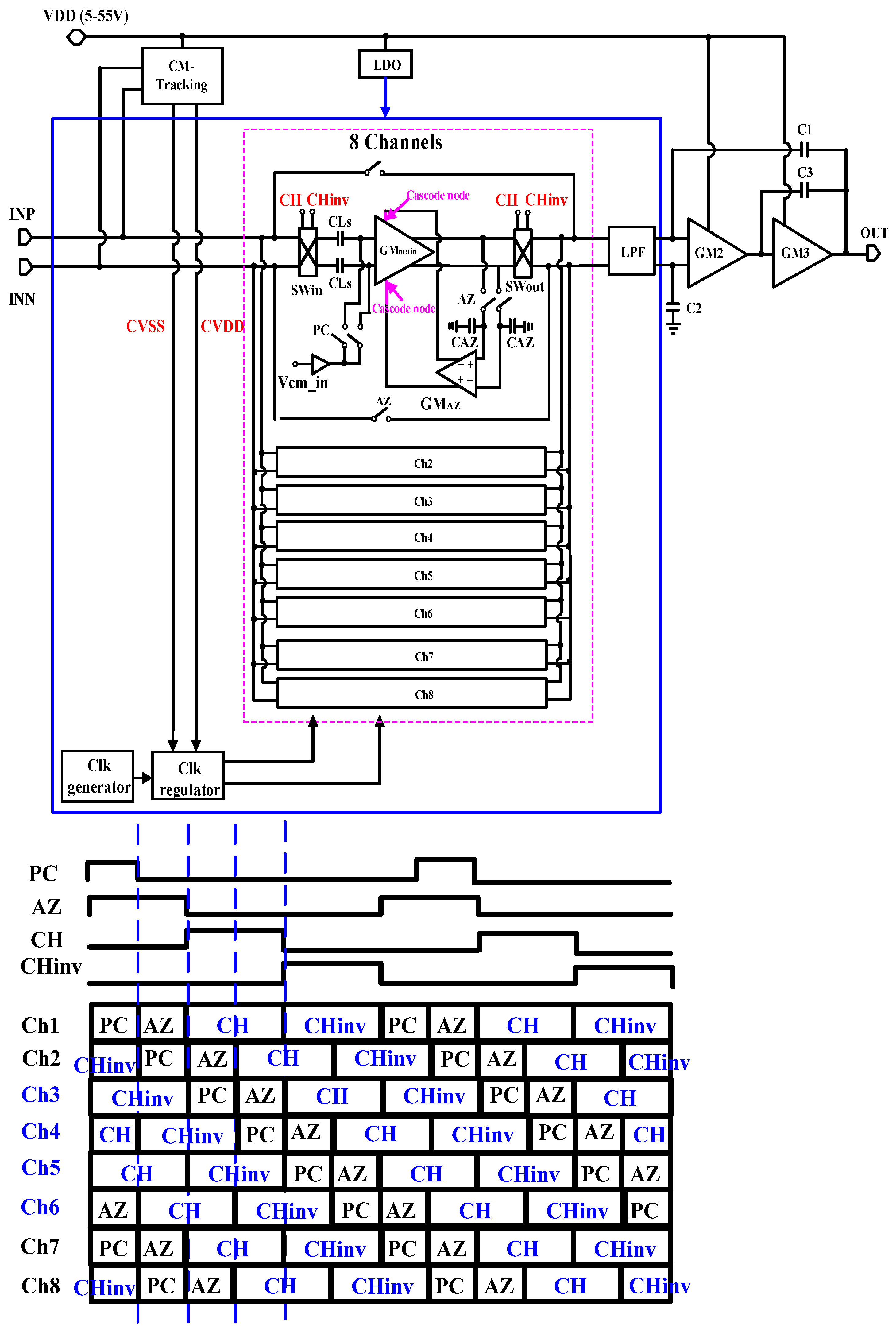
The structure and timing of the proposed OPA are shown in
Figure 1. The OPA adopts a three-stage structure. The amplification path includes an eight-channel main transconductor (
Gm1), a low-pass filter, second and third transconductors (
Gm2 and
Gm3), and frequency-compensation capacitors (
C1,
C2, and
C3). The input chopper SWin and output chopper SWout are controlled by two-phase non-overlapping clock signals generated by the clock generator and clock regulator. The low-pass filter is a first-order RC filter structure. LDO always generates a voltage of 4.5 V under a power supply of 5–55 V, supplying power to the main transconductor and auxiliary circuit. The second and third transconductors are powered by the power supply voltage. CM-tracking is a common-mode voltage tracking circuit that generates a voltage difference of approximately 1.8 V between two channels. As the power source and ground of the transistor in chopper, its main function is to ensure that the gate-source and gate-substrate voltage of the chopper are constant, and to reduce the body effect. The unit gain bandwidth
, second pole
, and third pole
of the OPA are, respectively, represented as
Usually, it must satisfy and , and a phase margin of 60 degrees will be achieved to stabilize the frequency characteristics of the OPA. Therefore, when , , , and are approximately equal, larger and are required. They are also the main source of power consumption for OPAs.
The main transconductor is an eight-channel Ping-Pong structure that combines auto-zero and chopper. The circuit is divided into three phase stages: pre-charge (PC), auto-zero (AZ), and chopper. The first and seventh channels are in the PC phase, the second and eighth channels are in the AZ phase, and the other four channels are in the chopper amplification phase. Compared with previous designs such as [
15], which utilized a six-channel ping-pong architecture, the proposed eight-channel structure allows for finer time-domain interleaving and longer available integration time per channel. This not only improves the timing margin for sampling and modulation, but also reduces the operating frequency of each individual path, thereby effectively lowering overall power consumption while maintaining high resolution. Therefore,
. The operating principle is as follows: in the PC phase, the output terminal of the main transconductor is open, and the input capacitor CLs first acts as a DC blocking capacitor to shield the common-mode voltage of sensor signal. The right plate of the CLs is pre-charged through the common-mode signal Vcm_in to provide input common-mode voltage for OPA. At the same time, the CLs serves as a coarse auto-zero capacitor, and the sampled input offset is cancelled out in the AZ phase, achieving input auto-zero; in the AZ phase, the output terminal of the main transconductor is open, and the output auto-zero transconductor Gm
AZ forms local feedback to sense the offset at output terminal, and feeds it back to the cascode node, which constructs an output fine auto-zero mechanism.
The offset at this time can be expressed as
is the original offset of , is the transconductance of GmAZ, and is the output resistance of GmAZ. After the AZ phase ends, the output terminal of the main transconductor is connected to a low-pass filter, and then it enters the two-phase chopper stage to amplify the signal. After passing through a low-pass filter, the high-frequency ripple in the output signal is filtered out. Thereby, precise amplification of the signal is achieved.
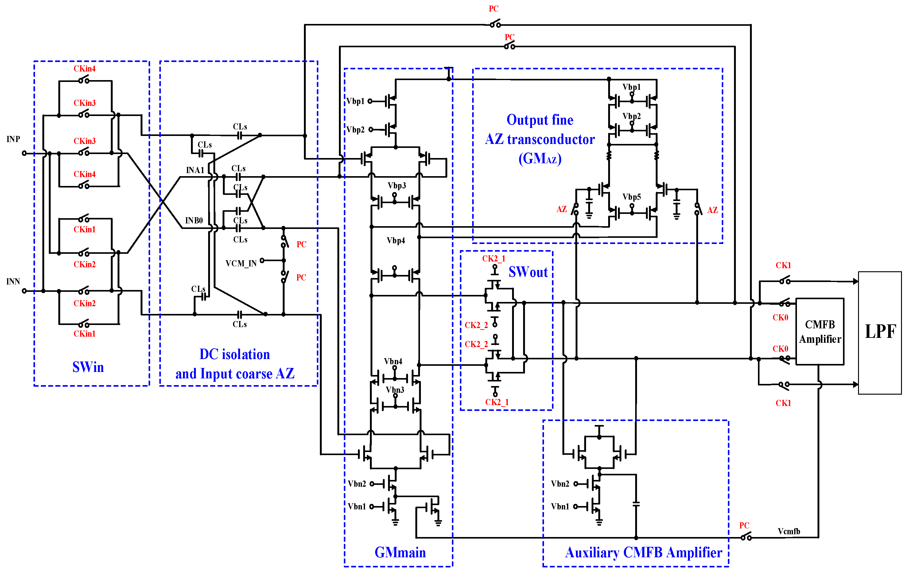
The core of
is a rail-to-rail fully differential telescope single-stage amplifier with input and output auto-zero, as shown in
Figure 2 [
16]. Note that
Figure 1 is a simplified block diagram intended to illustrate the signal flow and timing of the amplifier. In the actual implementation shown in
Figure 2, multiple level-shifting capacitors (CLs) are used instead of the two symbolic ones shown in
Figure 1. These capacitors serve to block DC components and enable the implementation of the three-phase operation—precharge (PC), auto-zero (AZ), and chopper amplification—by isolating the common-mode voltage and sampling the input offset. The use of additional bias voltages (Vbp3, Vbp4, Vbn3, Vbn4) allows precise biasing of the cascoded transistors, ensuring all devices remain in saturation. This helps increase the overall output impedance and open-loop gain. Although this adds biasing complexity, it is a reasonable trade-off for improved performance under a 4.2 V supply.
Additionally, the VCm_in shown in
Figure 1 as a unified input is practically realized by two separate sources: during the PC phase, the NMOS differential pair receives a fixed 1.6 V common-mode voltage from an external reference, while the PMOS differential pair receives the output common-mode voltage of 1.8 V. These two voltages jointly constitute the effective VCm_in and are abstracted as a single node in
Figure 1 for simplicity.
The DC blocking and input coarse AZ circuit is used to first isolate the common-mode voltage of input signal by the CLs. Meanwhile the input common-mode voltage in the right plate of the CLs is loaded to Gmmain in the PC phase, and the offset of Gmmain is sampled in the AZ phase to complete the coarse auto-zero operation; Gmmain uses symmetrical NMOS differential input pairs and PMOS differential input pairs to achieve rail-to-rail input; the output fine AZ transconductor samples the offset of the previous cycle in the AZ phase and feeds it back to the Gmmain cascode node as compensation current to reduce the offset by .
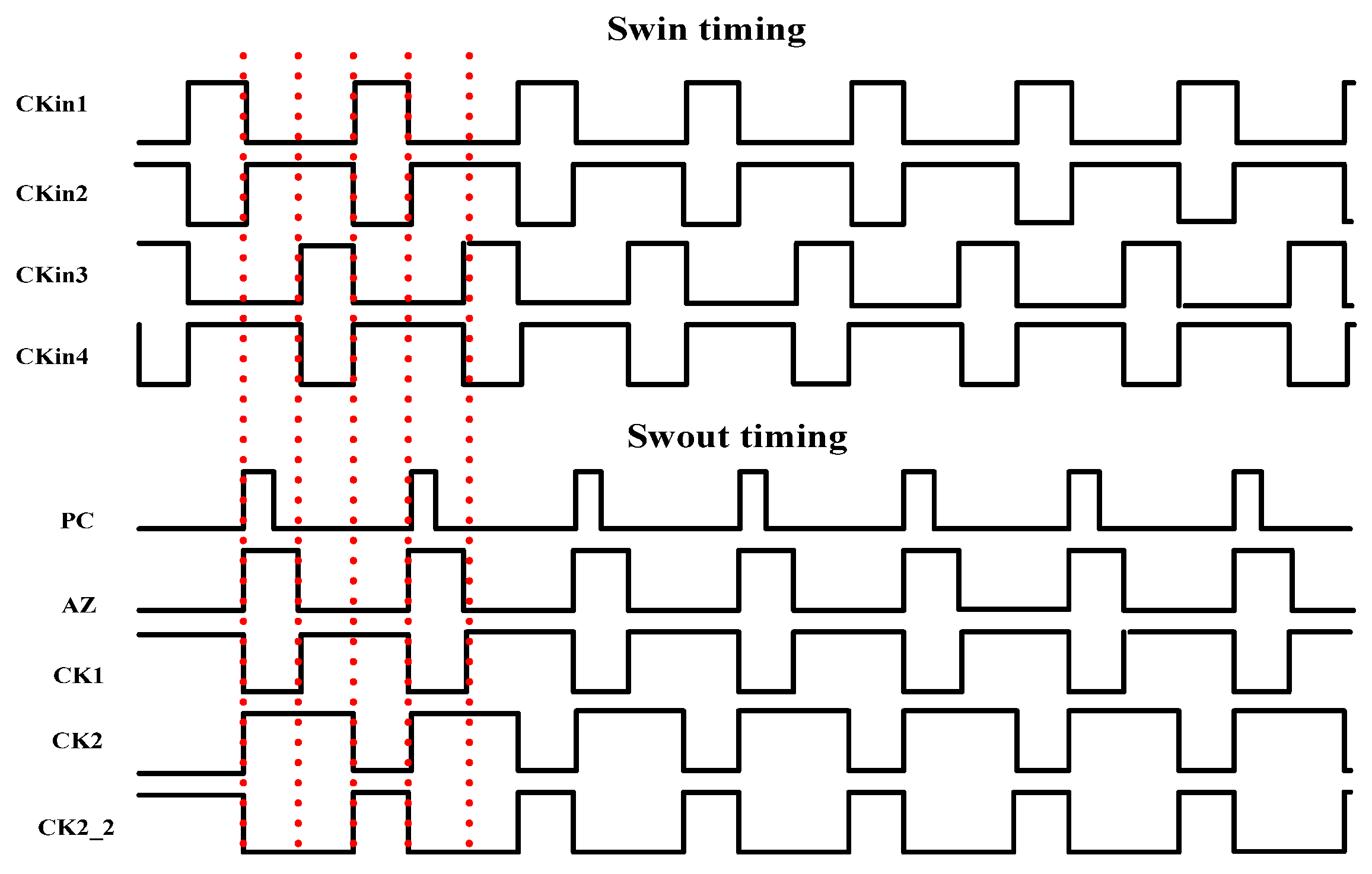
The timing of Gm
main is shown in
Figure 3. Gm
main first enters the PC phase CK0, inputs the common-mode voltage to the differential input terminal, and outputs the common-mode voltage to the common-mode feedback amplifier. Furthermore, the input and output of the PMOS differential input pair are short to clear residual charges; at the same time as the PC phase starts, the auto-zero phase starts, and its duration is twice the PC phase; at the beginning of the PC phase, Gm
main enters the first input chopper cycle (CKin2), and the other three chopper timings start working in sequence; at the beginning of the PC phase, Gm
main also enters the first output chopper cycle (CK2), and outputs the amplified signal to the low-pass filter in the CK1 phase after the auto-zero phase ends.
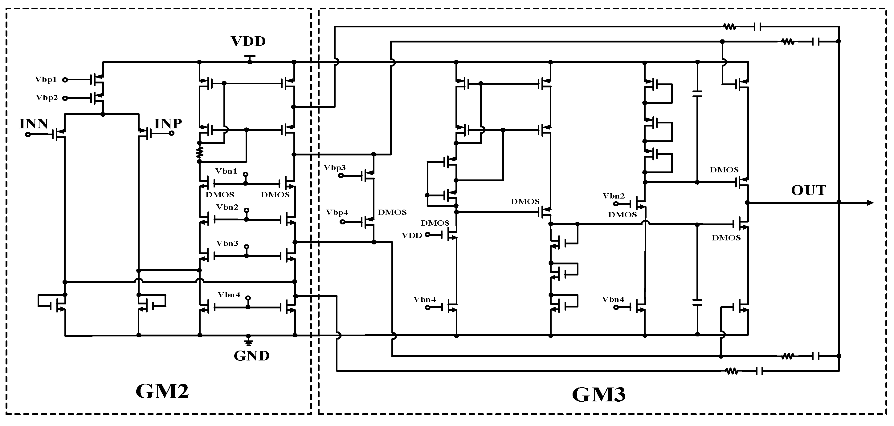
GM2 and GM3 are shown in
Figure 4. GM2 and GM3 are designed with DMOS to ensure that the output can recover to a range of 5–55 V based on the power supply voltage. GM2 is a two-stage folded cascode structure with PMOS input. GM3 is a Class-AB transconductor that utilizes floating voltage bias to ensure rail-to-rail output. Both Miller compensation and cascode compensation are used between GM2 and GM3 to stabilize their frequency characteristics. The simultaneous application of two compensation techniques is beneficial for pushing the third pole to a higher frequency, thereby reducing the transconductance of GM3 and decreasing power consumption [
17,
18].
The chopper switch is composed of MOS transistors, with the source connected to the input signal, the gate controlled by two-phase non-overlapping clock signals, and the substrate connected to ground. The voltage of the clock signal is equal to the power supply voltage. In high-voltage chopper OPAs, the power supply voltage usually varies within the range of 5–80 V, and the DC common-mode voltage of the input signal also changes accordingly. The changes in these two factors can cause drastic fluctuations in the gate-source and gate-substrate voltage of MOS transistors in chopper switches, deteriorating transistor body effects, causing fluctuations in transistor threshold voltage, and increasing errors caused by charge injection; furthermore, this causes a change in on-resistance of the switch, which has a nonlinear effect on the output signal.
This paper proposes a common-mode voltage tracking circuit that uses two amplifiers with a gain of approximately one to extract the common-mode voltage from the differential input of chopper amplifier. It generates a corresponding high control voltage signal and low control voltage signal, so that the gate and substrate voltages of the MOS transistor in chopper switch follow the changes of common-mode voltage in differential input. Thereby, it ensures the constant gate-source and gate-substrate voltage of the MOS transistor, reducing the body effect and maintaining a constant on-resistance, which finally keeps high-precision signal output. The common-mode voltage tracking circuit is shown in
Figure 5.
The chopper switches operate in a floating voltage domain provided by the common-mode tracking circuit. Specifically, the local ground is set to the input common-mode voltage (Vcom), and the local supply is Vcom + 1.6 V. This keeps the voltage across all transistors within 1.6 V, allowing the use of low-voltage planar CMOS devices without requiring DMOS transistors.
The high control voltage generator is a single-stage buffer powered by a supply voltage ranging from 5 V to 55 V, and achieves a unity gain. The differential input terminals INN and INP receive the differential input signals from the chopper amplifier and generate a high control voltage Voh,
This generated voltage Voh serves as the floating power rail for the two-phase non-overlapping clock generator and the low control voltage generator. The main structure of this amplifier consists of differential input transistors Mn1 and Mn2, load resistors R1 and R2, and a tail current transistor Mn4. Transistors Mn9, Mn10, Mn11, and Mn12 form a clamp circuit that protects high-voltage nodes from transient overvoltages. Specifically, Mn9, Mn10, and Mn11 operate as diode-connected MOSFETs within the clamp circuit. The amplifier’s biasing is established by transistors Mp1, Mp2, Mp3, Mn3, Mn5, Mn6, Mn7, and Mn8, along with resistors R3 and R4. When Voh rises sufficiently, Mn3 is activated, connecting the tail current transistor Mn4 in parallel with the bias current source, thereby jointly supplying the amplifier’s tail current.
The low control voltage generator is implemented as a single-stage amplifier using transistor splitting to replicate and output the common-mode voltage directly:
This ensures accurate tracking of the input common-mode voltage level.
3. Post-Simulation Results
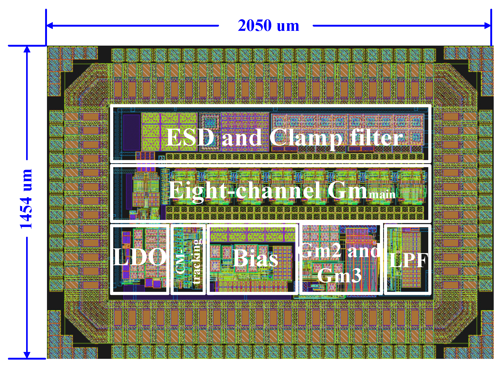
The proposed design is implemented by CMOS 180 nm BCD process. The layout of OPA is shown in
Figure 6 with an overall area of 2.98 mm
2. All the simulation results in this section are based on post-layout simulations.
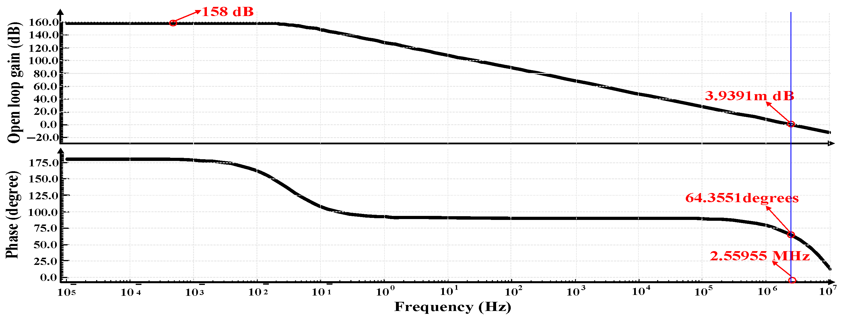
When load is 10 k and 50 pF, the simulation results of open-loop gain and phase margin are as shown in
Figure 7. The open-loop gain reaches 158 dB, the phase margin is 64.3 degrees, and the unit gain bandwidth is 2.55 MHz.
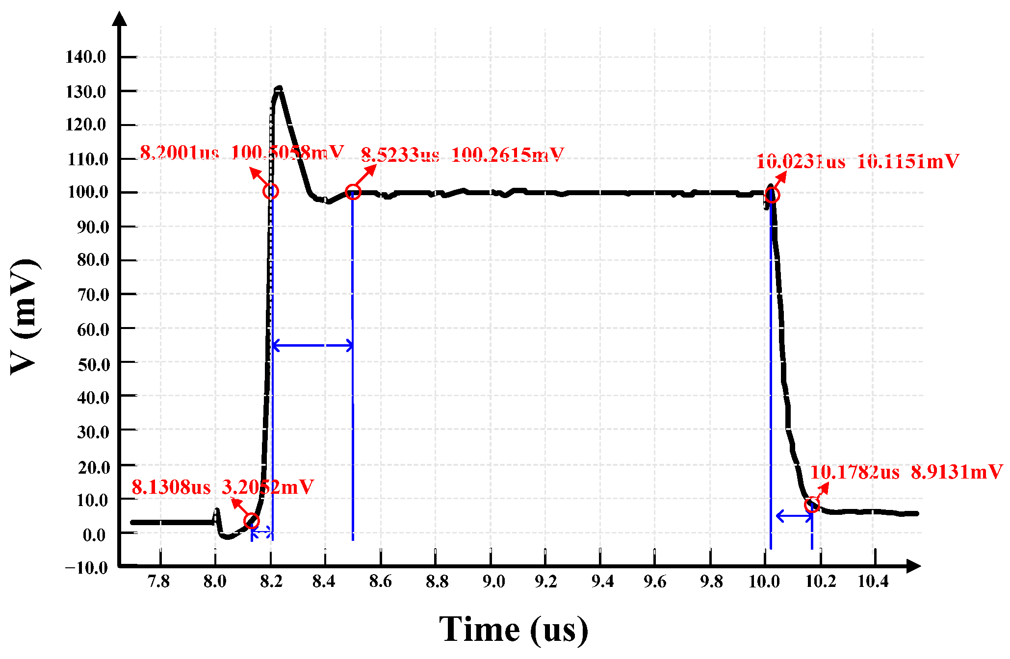
When configured as a unity gain structure and the input signal amplitude is 100 mV, the step response of the OPA is as shown in
Figure 8. The rise time is 0.07 us and the fall time is 0.155 us. Meanwhile, it only takes 0.32 us to settle within a 0.1% error range, which shows it has fast settle time and good accuracy.
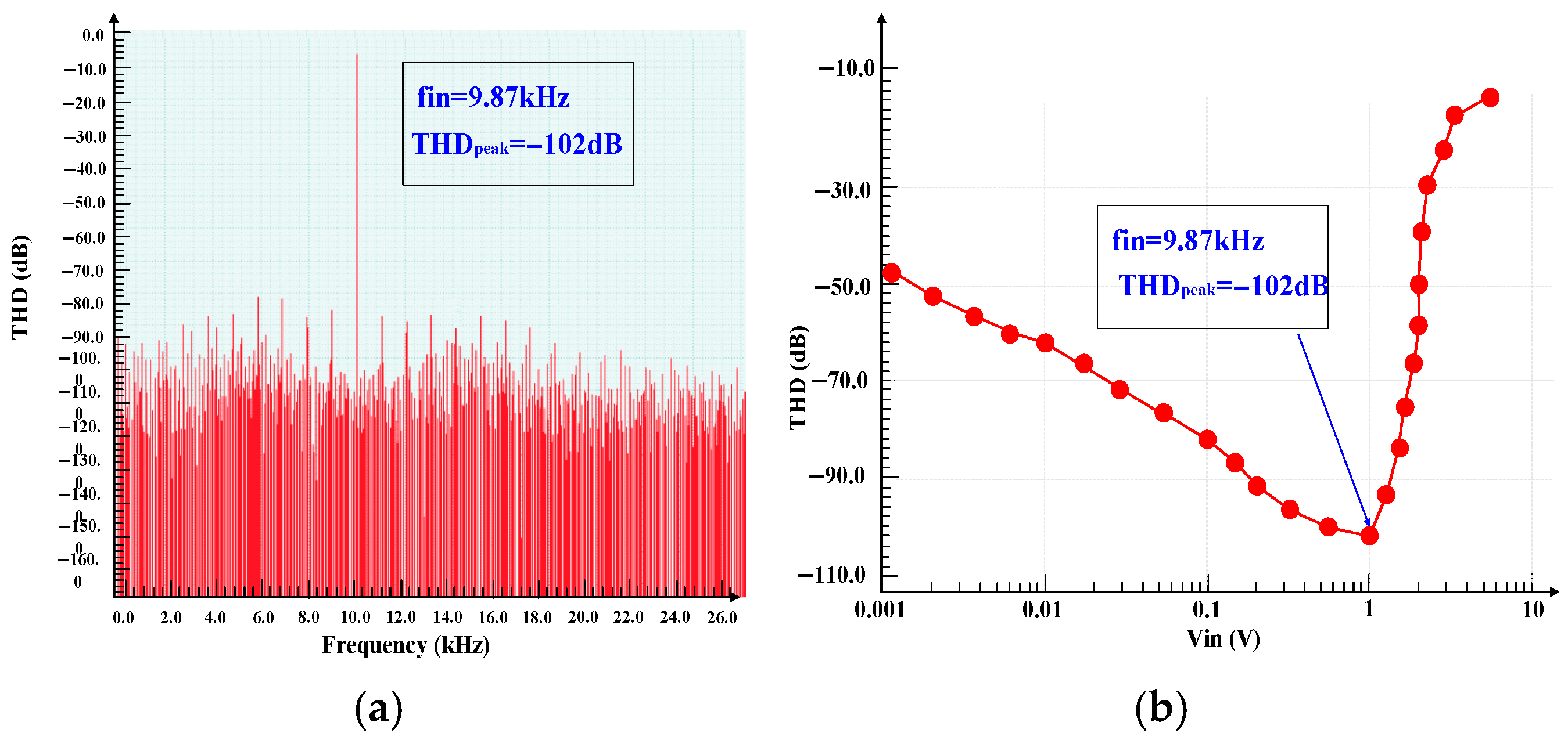
When the OPA is configured as a closed–loop unit gain structure, with an input signal frequency of 9.87 kHz and an amplitude of 1 V, the output spectrum is as shown in
Figure 9a. The peak total harmonic distortion (THD) is −102 dB.
Figure 9b demonstrates the relationship between input amplitude and THD. Peak performance of −102 dB is obtained with the input signal frequency of 9.87 kHz and amplitude of 1 V. When the input amplitude is closed to 2 V, the THD starts to get worse, Furthermore, it falls to about −12 dB while the amplitude reaches 5 V.
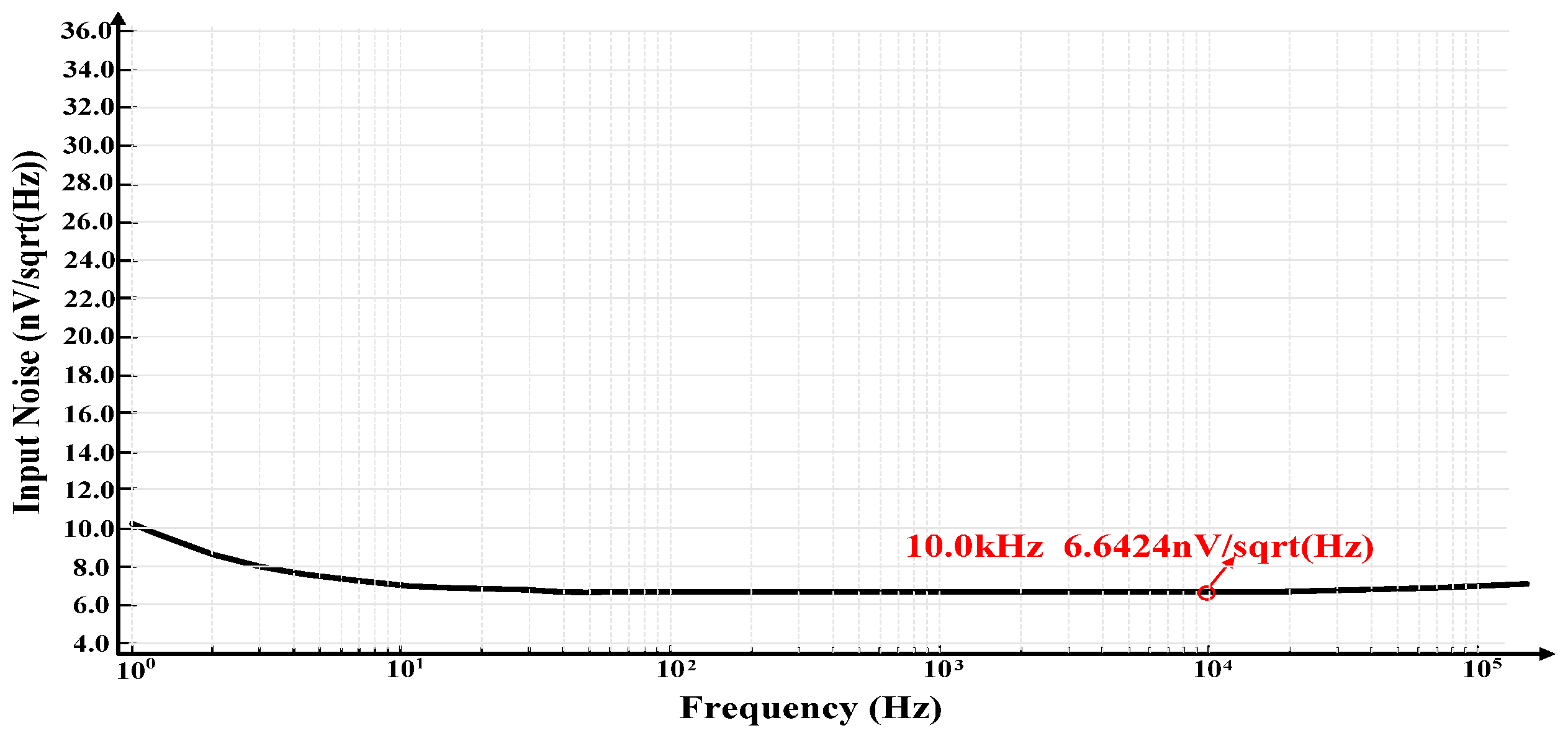
The noise PSD is presented in
Figure 10. The noise PSD is only 6.6 nV/√Hz at 10 kHz.
CMRR and PSRR versus frequencies are shown in
Figure 11. Due to the on-chip LDO, CMRR achieves 137 dB. PSRR+ and PSRR− are 131 dB and 101 dB, respectively.
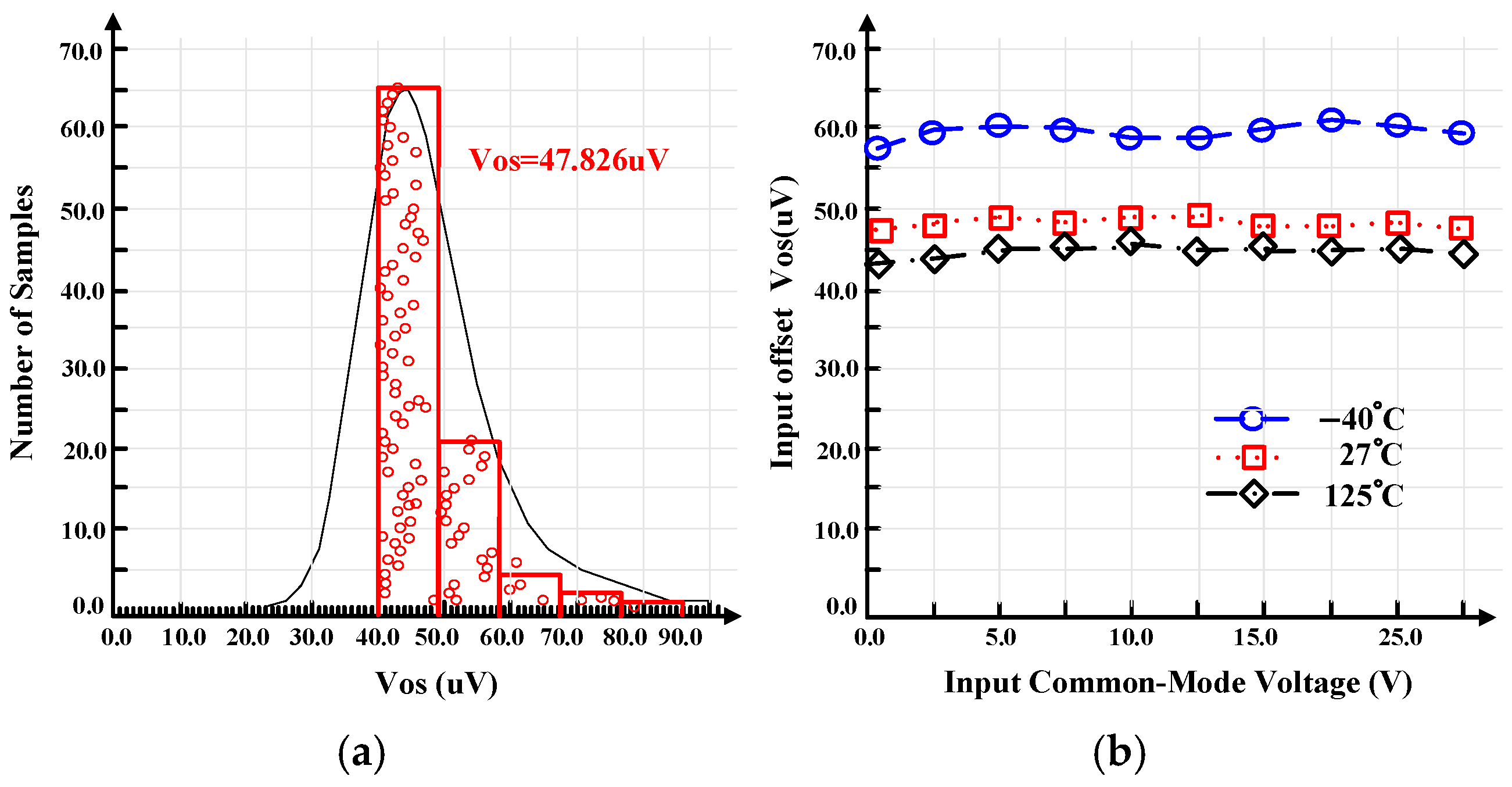
The combination of auto-zero and chopper technology effectively suppresses input offset. The offset is less than 47.8 µV, as shown in
Figure 12a. Thanks to the common-mode voltage tracking circuit, the input offset versus input common-mode voltage is as shown in
Figure 12b. With the variation of input common-mode voltage, the input offset varies in the range of 45–60 µV.
The comparison results of this work with others are shown in
Table 1. The OPA achieves a compromise design between input offset, noise, and power consumption under high power supply voltage. Without trimming after fabrication, the input offset of our work is a little larger than other works.
