Article

A 0.81–1.46 ppm/C High-Order Segmented Curvature-Compensation Bandgap Reference with Dynamic Element Matching Offset Cancellation for a Battery Management System

1
School of Electronic Science and Engineering, Xiamen University, Xiamen 361005, China
2
GeoMicro Devices (Xiamen) Co., Ltd., Xiamen 362000, China
3
Department of Electrical Engineering, Universiti Malaya, Kuala Lumpur 50603, Malaysia
*
Author to whom correspondence should be addressed.
Electronics 2025, 14(7), 1322; https://doi.org/10.3390/electronics14071322
Submission received: 20 January 2025 / Revised: 2 March 2025 / Accepted: 17 March 2025 / Published: 27 March 2025
(This article belongs to the Topic Advanced Integrated Circuit Design and Application)

Abstract

:
A precise high-order segmented curvature-compensation bandgap reference (BGR) with dynamic element matching (DEM) offset cancellation has been developed. The proposed segmented curvature-compensation scheme with a resistive trimming network is used to reduce the errors caused by the nonlinear dependence of the bipolar transistor base-emitter voltage ( V BE ) on temperature. To decrease the std dev ( σ ) of the reference voltage ( V REF ), DEM technology is applied in the core BGR to alleviate the current branch mismatch, as well as the current mirror mismatch in the error amplifier. The proposed BGR circuit is designed on a 0.18 μ m BCD process with an active area of 300 × 375 μ m and 61.5 μ A@5 V current consumption in the bandgap core circuit. The post-simulation results show that the proposed BGR achieves a temperature coefficient (TC) of 0.81–1.46 ppm/°C from −40 °C to 125 °C and a 0.045% σ / μ variation on a 3.2768 V V REF .

1. Introduction

High-performance battery management systems (BMSs) have become indispensable electronic devices in automotive electronics [1]. To accurately measure the state of charge of a battery over an operating temperature range, a precise reference voltage ( V REF ) with low temperature drift is required [1,2]. For a BMS, a 3.28 V reference voltage with a temperature coefficient (TC) less than 5.5 ppm/°C over a −40 °C to 125 °C temperature range is required to detect a 3 mV battery voltage change, which is still a great challenge in CMOS and BCD processes [1,3]. Moreover, process variations and device mismatches are also the main sources of residual non-proportional-to-absolute-temperature (non-PTAT) errors in the reference voltage after trimming [4], which significantly impacts the achievable precision of the bandgap reference voltage.
To maintain high accuracy in a wide temperature range, higher-order compensation circuits are used to correct the nonlinear dependence of base-emitter voltage ( V BE ) on temperature. The first-order temperature-compensated bipolar junction transistor (BJT)-based bandgap references (BGRs) are typically in the range of 20–100 ppm/°C [5,6,7,8], while the curvature or variation of V BE can be several mV over the temperature range from −40 °C to 125 °C [9]. BGR [1] utilizes the exponential characteristics of the base current and the resistance between the bases of BJT to perform the corrections. To achieve 4.6 ppm/°C TC over a wide temperature range of −40 °C to 130 °C, the curvature of subthreshold-operating MOSFETs is considered to further compensate for high-order temperature effects [1]. A curvature-compensated CMOS BGR circuit with a shared offset-cancellation method for internal amplifiers [10] adopts a multi-section curvature compensation method to alleviate the error from the nonlinear dependence of V BE on temperature. A sub-ranging TC compensation technique for a current reference is proposed [11], which enables second-order TC compensation in a wide temperature range without chip-by-chip trimming or an external reference. It is difficult to ensure the accuracy of the output voltage if the high-order temperature compensation is realized without resistors [12]; therefore, resistive trimming networks are still common. However, the temperature coefficients (TCs) in most of the literature are in the single-digit ppm/°C range since the nonlinear dependence of V BE on temperature is not completely canceled [13]. Thus, achieving a sub-1 ppm/°C TC is still a great challenge in a standard CMOS process.
The primary contributors to the overall offset come from the non-PTAT opamp offset and core device mismatch, as these errors are magnified by the closed-loop gain in a BGR and affect the output. A single-trim BGR with trimming, β -compensation, and curvature correction can further reduce non-PTAT errors resulting from mismatches with dynamic element matching (DEM) techniques [2]. An auto-zeroing circuit using a shared offset-cancellation method for internal amplifiers [10] can reduce the output inaccuracy within ±4.6 μ V with a relatively small die area. With the use of chopping to cancel the opamp offset and curvature correction to reduce the temperature dependency of the V BE , a CMOS bandgap reference achieves a 3 σ inaccuracy of ±0.15% from −40 °C to 125 °C [9]. In order to reduce the Δ V BE mismatch, a DEM technique is introduced in the V BE generation circuit [14]. The feedback coefficient enhancement technique is used to suppress the low-frequency noise and offset voltage [15].
In this article, a high-order segmented curvature compensation bandgap reference with DEM offset-cancellation is presented. In order to reduce the errors caused by the nonlinear dependence of a bipolar transistor V BE on temperature, a segmented curvature compensation scheme with a resistive trimming network is proposed. DEM technology has been applied in the core BGR to alleviate the current branch mismatch, as well as the current mirror mismatch in the error amplifier. The principles of curvature compensation and trimming and the current mismatch are analyzed. The effectiveness of the proposed curvature compensation scheme in reducing TC and DEM technology in output offset cancellation is verified through simulation in a 0.18 μ m BCD process, achieving a maximum TC of 1.46 ppm/°C and a maximum σ / μ variation of 0.049% within −40 °C to 125 °C.
The rest of this paper is organized as follows. The proposed high-order segmented curvature-compensation scheme with resistive trimming network and DEM offset cancellation are discussed in Section 2. In addition, a complete circuit architecture for the proposed BGR design is demonstrated in detail. The simulation results are presented in Section 3 and compared with the state of the art. Finally, the conclusion is drawn in Section 4.

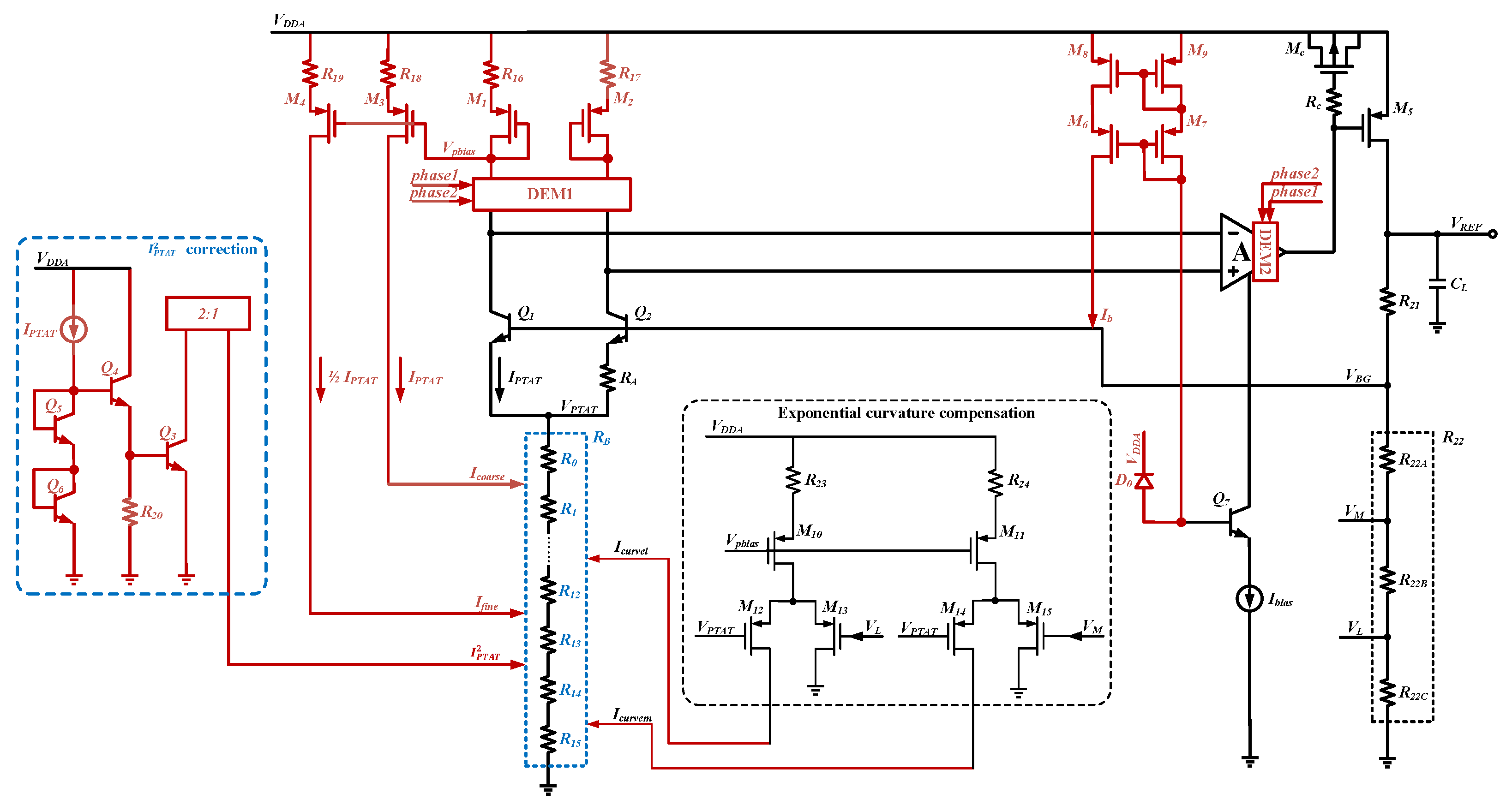
2. Proposed Design and Architecture

2.1. Proposed High-Order Segmented Curvature Compensation

Figure 1 shows the mathematical signal processing diagram illustrating how the final V REF is obtained with correction currents in the proposed high-order segmented curvature-compensation method. The trend of a first-order compensated V REF is illustrated in Figure 1a. To improve the TC over a wide temperature range, the V REF compensation is divided into three temperature segments, defined by the T 1 and T 2 points, as shown in Figure 1, with each segment being compensated by distinct correction currents. In the high-temperature segment, the I PTAT 2 is introduced to perform the correction above the T 2 temperature point. The temperature drift curvature can be compensated from Figure 1a–c. In the low-temperature and middle-temperature segments, the I curvel and I curvem are introduced to perform the exponential curvature correction under T 2 temperature point. So I curvel mainly provides correction under a T 1 temperature point, while I curvem provides fine-tuning correction in the [ T 1 , T 2 ] segment. This leads to the curvature being compensated from Figure 1c–e and finally to Figure 1g. These high-order segmented curvature-correction currents can be converted into voltage through the resistors and further fine-tuned using the proposed trimming network.
Bandgap cores typically use BJT devices to derive the bandgap voltage of silicon [1,2,3,4]. The emitter-base voltage of BJT is commonly used in precision voltage references due to its robust operation over the process [2]. The topology of the BGR with high-order segmented curvature compensation is presented in Figure 2. The bandgap core is based on the high-order curvature-compensated BGR [1], as shown by the black line in Figure 2. However, the main difference is in the first-order compensation, I PTAT 2 correction, and trimming modules. Compared with the BGR [1], M1–M4 is introduced to generate a PTAT correction current. Q3–Q6 and R20 are introduced to generate the I PTAT 2 correction current. Furthermore, RB is divided into R0 to R15 to implement the proposed trimming scheme.
The proposed BGR includes the bandgap core, base current compensation module, first-order and higher-order curvature compensation modules, trimming module, and offset-cancellation module. The core BGR is implemented with a three-stage cascade configuration. The presence of the inherent output stage circuit enables the BGR to drive the load. Resistors RC and PMOS capacitors MC are added for loop stability. The base current compensation method [1] is used to reduce the impact of the BJT base input resistance. The base correction current I b is generated by the biased base current of the BJT Q7. Compared with the BGR [1], the resistor between bases of BJT is removed and adjusted using M6–M9 instead to control the base current magnitude. Generally, the bandgap core voltage V B G is given by [1]
V B G = V B E 1 + 2 R B I P T A T = V B E 1 + 2 R B R A · Δ V B E = V B E 1 + 2 R B R A · V T ln ( N ) = V B E 1 + 2 R B R A · k T q ln ( N )
where I PTAT is the current flowing through resistor RA, V BE is the BJT’s base-emitter voltage, Δ V BE = V T ln ( N ) is the base-emitter voltage difference between Q1 and Q2, and N is their emitter area ratio. V T = k T / q is the thermoelectric coefficient, where k is the Boltzmann constant, T is the absolute temperature, and q is the elementary charge. Based on the above equation, it can be seen that selecting appropriate values for N and R A can draw the I PTAT current. In this work, the area ratio of Q1 and Q2 is set to 8. To enhance the matching of Q1 and Q2, the layout places Q1 at the center and arranges eight equal-sized unit devices for Q2 in a common centroid configuration with interspersed dummy devices. A relatively temperature-independent reference voltage can be generated by selecting an appropriate R B . However, the V BE of a BJT is not a purely linear function of temperature.
The relationship between V BE and temperature can be expressed as follows [1,2]:
V B E ( T ) = V G 0 ( T r ) V G 0 ( T r ) V B E ( T r ) T T r ( η ξ ) V T ln T T r
where V G 0 ( T r ) is the extrapolated bandgap voltage at a reference temperature T r , η is a process-related constant, and ξ is the order of the collector current temperature dependence. V G 0 ( T r ) V B E ( T r ) T / T r is the first-order linear temperature dependence term of V BE . And based on Equation (1), selecting the appropriate R B and I PTAT can eliminate it. ( η ξ ) V T ln T / T r is the high-order nonlinear temperature-dependent term of V BE , which requires high-order curvature compensation.
In Figure 2, I coarse is the first-order coarse trimming correction current. I fine is the 1st-order fine-trimming correction current. I PTAT 2 , I curvel , and I curvem are high-order curvature correction currents in the high-, low-, and medium-temperature ranges, respectively. In order to generate the I PTAT 2 correction module, it is composed of Q3–Q6, R20, and the relationship of V BE between Q3–Q6 can be expressed as
V B E 5 + V B E 6 = V B E 3 + V B E 4
So the current flowing through BJT Q3 is given by
I C 3 = I C 5 I C 6 I C 4 = I PTAT 2 I C 4 = I PTAT 2 R 20 V B E 3
The first-order coarse correction coefficient is α 1 = R e q , c o a r s e / R B , where R e q , c o a r s e represents the equivalent resistance from the I coarse node to ground. Similarly, the first-order fine correction coefficient is α 2 = R e q , f i n e / R B , where R e q , f i n e represents the equivalent resistance from the I fine node to the ground. And the I PTAT 2 correction coefficient is α 3 = R e q , I PTAT 2 / R B , where R e q , I PTAT 2 represents the equivalent resistance from the I PTAT 2 node to the ground. Regardless of I curvel and I curvem , according to Figure 2 and based on Equation (1), the expression for V BG can be rewritten as
V B G ( T ) = V B E ( T ) + I P T A T R B 2 + α 1 + α 2 2 + I P T A T 2 R 20 V B E 3 R B α 3 2
Based on Equations (2) and (5), there is
V B G ( T ) = V G 0 ( T r ) V G 0 ( T r ) V B E ( T r ) T r k R B q R A 2 + α 1 + α 2 2 ln ( N ) T ( η ξ ) V T ln T T r + k R B q R A ln ( N ) 2 R 20 V B E 3 R B α 3 2 T 2
Expanding ln T / T r using a Taylor series expression, there is
V B G ( T ) = V G 0 ( T r ) V G 0 ( T r ) V B E ( T r ) T r k R B q R A 2 + α 1 + α 2 2 ln ( N ) 11 k 6 q ( η ξ ) T + k R B q R A ln ( N ) 2 R 20 V B E 3 R B α 3 2 3 k q 1 T r ( η ξ ) T 2 + 3 k 2 q 1 T r 2 ( η ξ ) T 3
Based on the above equation, it can be seen that if the coefficient term of T is zero, ( α 1 + α 2 / 2 ) R B can be determined. If the coefficient term of T 2 is zero, α 3 R B can be determined. In practical circuit design, further fine-tuning is required to achieve optimal TC.
Although the compensation is effective, the output reference voltage still exhibits a downward parabolic curvature with temperature changes. To improve the TC of V REF in the low to medium temperature range, the exponential curvature compensation method [1] is also implemented in the design, as shown in Figure 2. Compared with the BGR [1], the I CO = I curvel + I curvem in [1] is divided into two current paths, I curvel and I curvem , which are used for temperature drift correction under the T 2 temperature point. The I curvel correction coefficient is α 4 = R e q , curvel / R B , where R e q , curvel represents the equivalent resistance from the I curvel node to the ground. Similarly, the I curvem correction coefficient is α 5 = R e q , curvem / R B , where R e q , curvem represents the equivalent resistance from the I curvem node to the ground. The final expression for the V BG can then be derived as
V B G t r i m ( T ) = V B G ( T ) + I curvel R B α 4 + I curvem R B α 5
From Equation (8), an appropriate resistance node in RB can be chosen to generate the suitable α 4 or α 5 . The proposed compensation scheme eliminates the need for fine-tuning the values of V M and V L to construct an I CO that is complementary and opposite in curvature to the V REF [1], making temperature drift correction more accurate and easier to control.

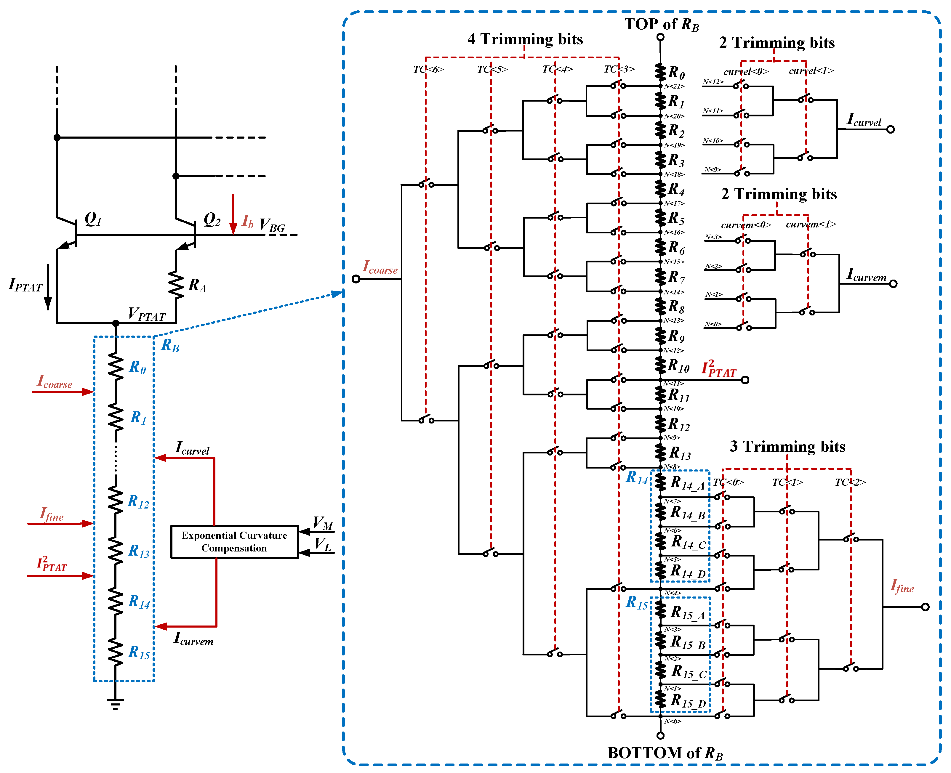
2.2. Trimming Scheme Implementation

Figure 3 shows the implementation of the proposed trimming scheme. The resistor RB is initially divided into R0 and a four-bit trimming network, consisting of 15 equal resistors from R1 to R15. By dividing resistors R14 and R15 into four equal segments, an additional three-bit trimming network is incorporated, resulting in a total seven-bit resistor network. By adjusting the trimming codes TC<6:0>, the first-order correction currents of I coarse and I fine can be injected into various resistor nodes N<21:0> to calibrate the first-order linear temperature coefficients. For curvature compensation trimming, a similar resistor network is employed to create two two-bit trimming networks. By adjusting the trimming codes curvel<1:0> and curvem<1:0>, the high-order correction currents of I curvel and I curvem can be injected into resistor nodes N<3:0> and N<12:9>, respectively, to calibrate the high-order temperature coefficients. All the trimming codes, including TC<6:0>, curvel<1:0> and curvem<1:0>, are generated by two-point temperature measurement. The more measurement points, the better the temperature coefficient that can be achieved.
The resistor divisions are determined based on the worst-case temperature drift and the required trimming range. Running TC simulations at various corners shows that the worst-case temperature drift before trimming occurs at the ss and ff corners. Specifically, the ss corner shows a temperature drift of −20.9 mV, while the ff corner shows a temperature drift of +38.7 mV. Therefore, the trimming range needs to cover at least 38.7 + 20.9 = 59.6 mV . So, the trimming range is set from −65 mV to +65 mV. Given a first-order correction current I coarse of 8 μ A and the four-bit trimming network, the resistance value for R1–R15 is 130 mV 15 × 8 μ A = 1.08 k Ω . Furthermore, R14 and R15 are divided into four equal parts for fine-trimming correction: 1.08 k Ω 4 = 271 Ω . Given a I fine of 4 μ A, this results in a first-order trimming resolution of 1 2 × 8 μ A × 271 Ω = 1.08 mV.

2.3. DEM Offset Cancellation

The device mismatch of the bandgap core current branch in Figure 2 significantly impacts the output voltage accuracy of the BGR. To analyze this mathematically, assuming A is an ideal operational amplifier, then V REF can be written as
V R E F = 1 + R 21 R 22 V B E 1 + 2 R B R A · V T ln I C 1 I C 2 / N = 1 + R 21 R 22 V B E 1 + 2 R B R A V T ln N 2 R B R A V T ln 1 + Δ I I 1 + R 21 R 22 V B E 1 + 2 R B R A V T ln N 2 R B R A V T Δ I I
where I is the current flowing through M1 and M2, and Δ I represents the current mismatch between these two branches. The offset of V REF can be expressed as
V O S , REF = 2 1 + R 21 R 22 R B R A V T Δ I I
According to Equation (10), it can be calculated that a 200 nA mismatch current between the bandgap core current branch results in approximately 15 mV − V OS , REF . Since the offset drift caused by mismatch between the bandgap core current branch is typically non-PTAT, it is difficult to reduce it with a PTAT trim. Increasing the value of current I can reduce the mismatch between the bandgap core current branch, but it will increase the power consumption relatively more. Therefore, the offset needs to be removed by offset-cancellation techniques [16]. In this work, a dynamic element matching (DEM) technology is employed to reduce non-PTAT errors related to device mismatches, as shown in Figure 4a.
In the timing control, p h a s e 1 and p h a s e 2 are two non-overlapping clock phases used to perform the DEM operation. As a result of the DEM operation, the V REF changes with the state of the control signals. In addition, the switches in DEM1 are located in the current branch of the bandgap core. Large MOSFET (50 μ m/0.5 μ m) are used for the resistor switches to minimize their on-resistance influence [13]. Within one conversion cycle, the average currents of M1 and M2 are maintained at a 1:1 ratio. The intermediate error amplifier in Figure 4b utilizes a cascode structure to achieve high loop gain and high common-mode rejection ratio (CMRR). Furthermore, to reduce the current mirror mismatch in the error amplifier, a DEM2 module, controlled by the same clock, is employed in this amplifier.
The DEM frequency is 1 kHz. Transient simulation shows that due to the parasitic coupling of high-frequency switching, there is a ripple of about 200 μ V in the output of the BGR, which will be superimposed with the offset on the BGR output. As mentioned in [11], the ripple from two-phase DEM can be removed using a switched-capacitor notch filter, or a discrete-time or continuous-time ripple-reduction loop (RRL), which is not included in this work. Transient simulation shows a static power consumption of 143.68 μ A without DEM, which increases to 143.73 μ A with the 1 kHz DEM clock, indicating that the impact of switching devices on power consumption is negligible.

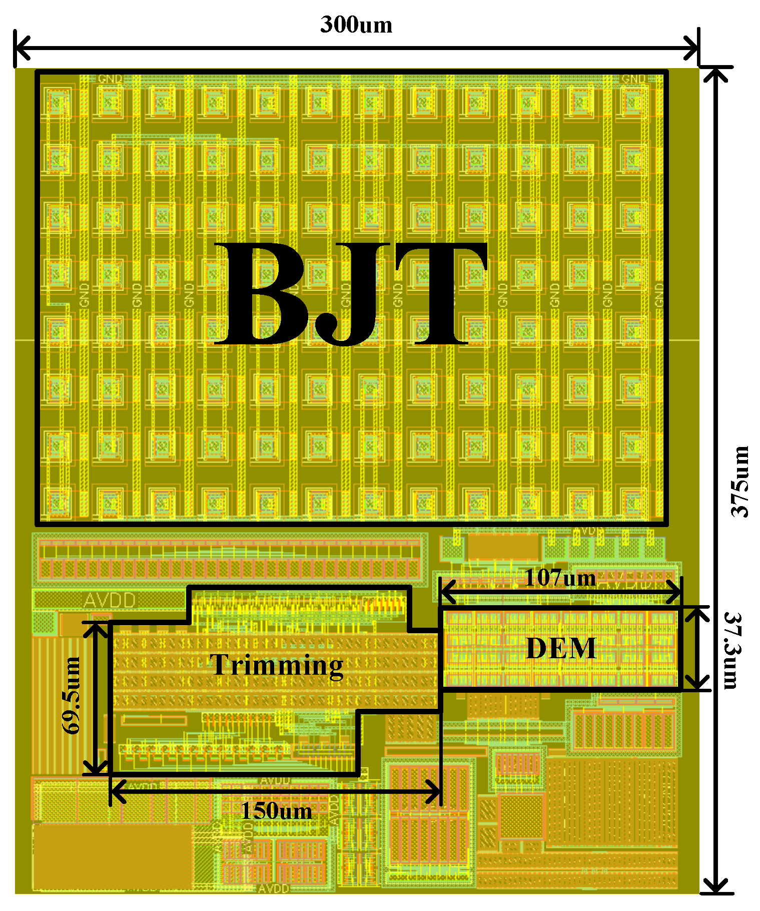
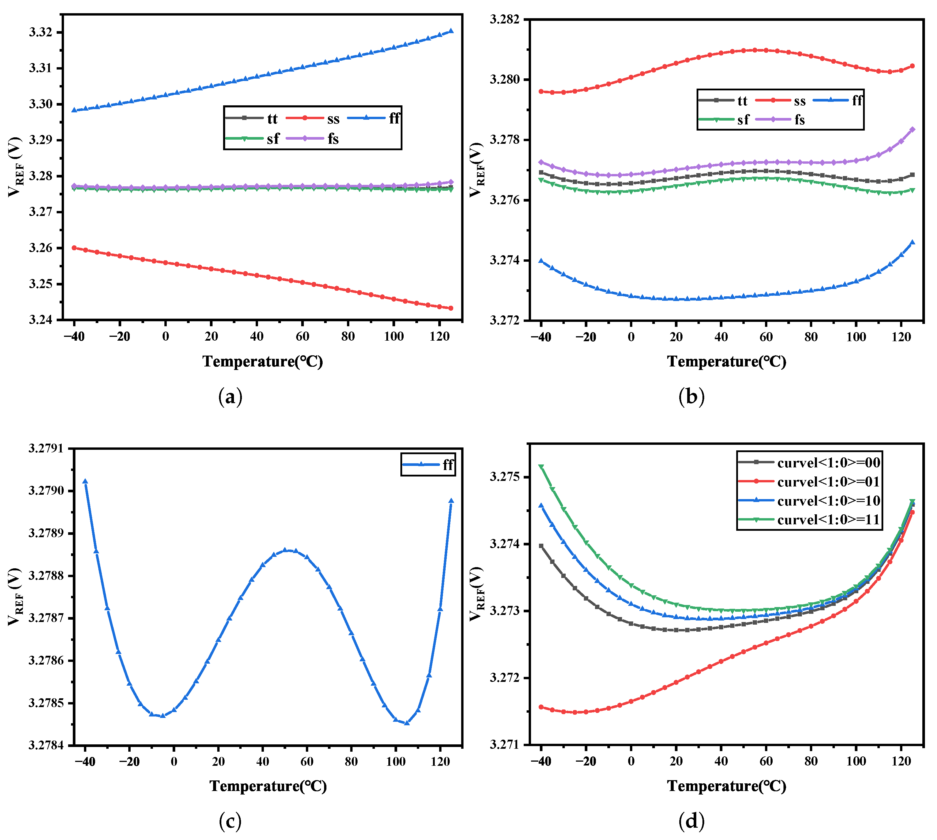
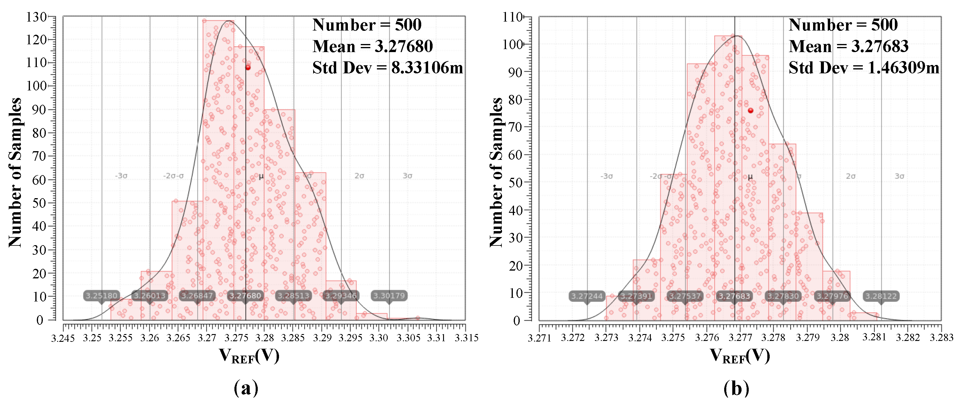
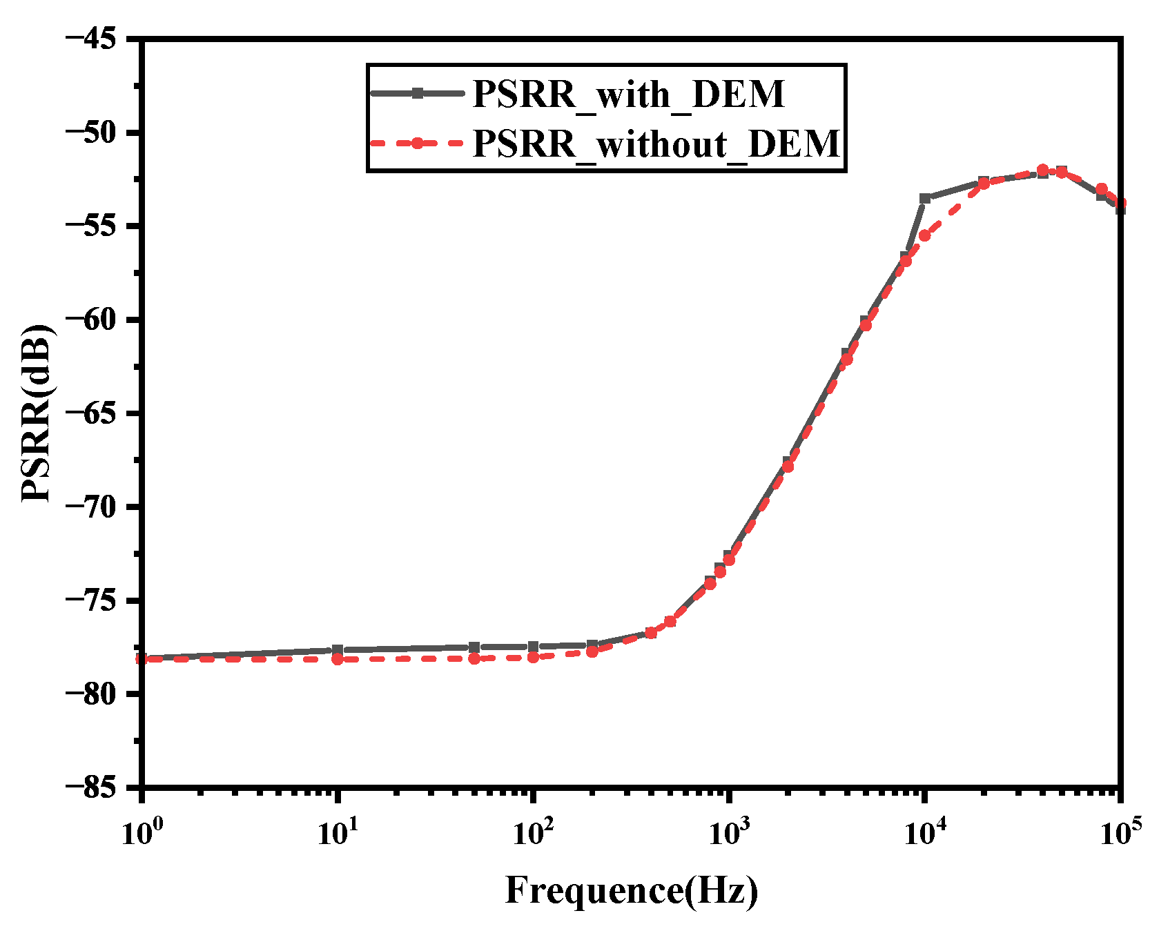
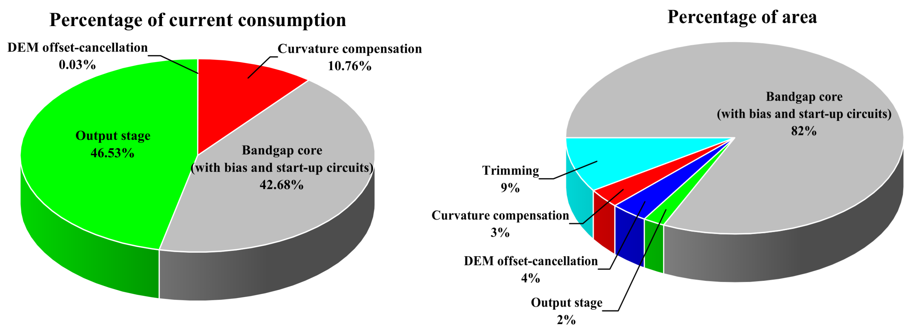
3. Simulation Results

The BGR is designed on a 0.18 μ m BCD process. The layout is shown in Figure 5, with an active layout area of 300 × 375 μ m. The active layout area of DEM offset cancellation is 107 × 37.3 μ m, while the layout area of trimming module is 150 × 69.5 μ m. Components with a deep n-well layer are chosen, since this can efficiently separate the p-substrate for different circuits and then block the noise from other subsequent circuits [17]. The designed BGR operates with a static current consumption of 144 μ A, of which 67 μ A is allocated to the output driving stage. Thus, the core of the proposed BGR only consumes 61.5 μ A. Unless otherwise specified, all post simulations were conducted at a typical temperature of 27 °C and a power supply voltage of 5.0 V.
Figure 6a shows the simulated V REF variation at different corners before trimming from −40 °C to 125 °C, with an output voltage of 3.2768 V at 27 °C. Figure 6b shows the simulated V REF variation at different corners after first-order trimming. The results demonstrate that the proposed curvature compensation scheme achieves a TC range of 0.81 to 3.48 ppm/°C and is robust against process variations. Figure 6c shows the simulated V REF variation for the ff corner after first-order trimming and curvature trimming. Figure 6d shows the simulated V REF variation across different curvel<1:0> trimming codes for I curvel curvature correction. Table 1 lists the TC simulation results of the BGR before/after first-order trimming and curvature trimming at different corners. All the data points are measured after post-simulation. It can be concluded that the range of V REF variation after trimming is between 0.44 mV and 0.79 mV, corresponding to a TC of 0.81–1.46 ppm/°C. We also study the BGR under extreme conditions (e.g., −50 °C or 130 °C) the circuit operates normally and the TC is 1.41 ppm/°C over a wide temperature range of −50 °C to 130 °C.
The first-order compensated V REF versus the I PTAT 2 correction voltage at the tt corner and the I PTAT 2 -compensated V REF versus I curvel correction voltage are plotted as simulated functions of temperature in Figure 7. The correction voltages generated by the I PTAT 2 and I curvel are I PTAT 2 × R e q , I PTAT 2 and I curvel × R e q , curvel according to Equation (5). The simulation results show the intersection points of the correction voltage curve and the pre-correction V REF curve around −4 °C and 82 °C at tt corner. The temperature points T 1 and T 2 are determined by simulation or measurement optimization. First, we perform I PTAT 2 correction, which reduces the voltage variation of V REF from 6.6 mV to 1.12 mV and the TC from 46.8 ppm/°C to 7.9 ppm/°C over the temperature range from T 2 to 125 °C. Second, the voltage variation of V REF is further reduced from 4.85 mV to 0.81 mV and the TC is improved from 41.1 ppm/°C to 6.9 ppm/°C over the temperature range from −40 °C to T 1 by applying I curvel correction. Finally, after applying I curvem correction, V REF achieves a TC of 0.81 ppm/°C across the entire temperature range from −40 °C to 125 °C. These improvements indicate that I PTAT 2 , I curvel and I curvem primarily contribute to the curvature compensation within the ranges of [ T 2 , 125 °C], [−40 °C, T 1 ], and [ T 1 , T 2 ], respectively. During this correction process, the trimming codes for this batch of the BGR circuit can also be determined.
Figure 8 shows the comparison of Monte Carlo simulation results of 500 sampling points with/without the proposed DEM offset cancellation. It can be seen that the mean ( μ ) of V REF with DEM offset cancellation is around 3.27683 V, remaining almost unchanged. The std dev ( σ ) of V REF decreased from 8.33 mV to 1.46 mV, and the σ / μ variation in V REF decreased from 0.25% to 0.045%, an improvement of 82%.
Figure 9 shows the simulated V REF vs. V DDA at different process corners. The simulation results show that when the power supply voltage increases from 4.2 to 6.0 V, the V REF changes by 0.38 mV at the tt corner, corresponding to a line regulation of 0.022%/V. Furthermore, at the worst-case ss corner, the V REF changes by 0.74 mV, corresponding to a line regulation of 0.041%/V. When the load current increases from 0 mA to 1.5 mA, the reference voltage changes by 33.1 μ V at the tt corner, corresponding to a load regulation of 0.022 mV/mA, while at the worst-case ss corner, the V REF changes by 35.8 μ V, corresponding to a load regulation of 0.024 mV/mA. The proposed BGR exhibits low and consistent sensitivities at all process corners.
Figure 10 shows the simulated power supply rejection ratio (PSRR) of the proposed BGR with/without DEM offset cancellation over the frequency range from 1 Hz to 100 kHz. At 10 Hz, the PSRR is approximately −78 dB, while at 100 kHz, the PSRR is approximately −54 dB. The PSRR with and without DEM offset-cancellation shows a negligible difference.
Figure 11 shows the current consumption and area of the proposed BGR circuit components. The DEM offset-cancellation module occupies 0.03% of the total current consumption and 4% of the layout area. The curvature-compensation modules consume 10.76% of the total current consumption and 3% of the layout area. Similar to [14,18], the current consumption in this design is 144 μ A, including the 67 μ A current consumption of the output stage, which can directly drive a load current ranging from 0 to 1.5 mA. The bandgap core’s current consumption is 61.5 μ A, which remains within a reasonable range when compared to the other bandgap reference circuits listed in Table 2. In the output driving stage, methods such as using shared feedback resistors [19] can be explored to enhance the current driving capability while minimizing the overall power consumption.
Table 2 compares the proposed BGR performance with other state-of-the-art works. For BGRs without offset cancellation, such as the design [1], this work can achieve a much smaller σ / μ variation. Compared with the design without curvature correction [14], this work achieves a much smaller TC and σ / μ variation. Even for those works with curvature compensation [2,9,10,18], this work exhibits the lowest TC, making it suitable for high-precision BMS applications. This demonstrates the effectiveness of the proposed segmented curvature-compensation scheme with the DEM offset cancellation. The design in [1] performs well in terms of temperature drift. However, controlling the correction current index trajectory through V M and V L values is challenging. In contrast, the proposed trimming scheme for this BGR circuit makes temperature drift correction more accurate and easier to control. Additionally, the proposed BGR utilizes DEM technology to alleviate the current branch mismatch, as well as the current mirror mismatch in the error amplifier, achieving σ / μ values similar to those in [2].

4. Conclusions

A high-order segmented curvature-compensation BGR with DEM offset cancellation is designed on a 0.18 μ m BCD process. The active layout area is 300 × 375 μ m, of which the DEM offset cancellation and trimming module occupy 107 × 37.3 μ m and 150 × 69.5 μ m, respectively. The proposed segmented curvature compensation scheme with a resistive trimming network can improve the TC performance to 0.81–1.46 ppm/°C over −40 °C to 125 °C. The DEM offset cancellation can improve the σ / μ variation in V REF by 82%, decreasing from 0.25% to 0.045%. The line regulation is 0.022%/V from 4.2 V to 6 V, while the load regulation is 0.022 mV/mA from 0 mA to 1.5 mA. The PSRR at 10 Hz frequency is −78 dB. The proposed BGR is highly suitable for integrated high-precision battery monitoring and power supply systems.

Author Contributions

Methodology, Y.L.; Investigation, W.W.; Writing—original draft, J.X.; Writing—review & editing, H.R.; Supervision, X.L. All authors have read and agreed to the published version of the manuscript.

Funding

This work was supported in part by the National Foreign Experts Project H20240900, in part by the Fujian Innovation Funding on Industry Academia Collaboration Research under Grant 2022H6004, in part by Xiamen Science and Technology Projects in Future Industries 2024, and in part by the Fujian Key Laboratory of Integrated Circuit (IC) Design and Measurement (Xiamen University).

Data Availability Statement

Data are contained within the article.

Conflicts of Interest

Author Yude Lin was employed by the company GeoMicro Devices (Xiamen) Co., Ltd. The remaining authors declare that the research was conducted in the absence of any commercial or financial relationships that could be construed as a potential conflict of interest.

References

  1. Zhu, G.; Yang, Y.; Zhang, Q. A 4.6-ppm/°C High-Order Curvature Compensated Bandgap Reference for BMIC. IEEE Trans. Circuits Syst. II Express Briefs 2019, 66, 1492–1496. [Google Scholar] [CrossRef]
  2. Boo, J.H.; Cho, K.I.; Kim, H.J.; Lim, J.G.; Kwak, Y.S.; Lee, S.H.; Ahn, G.C. A Single-Trim Switched Capacitor CMOS Bandgap Reference with a 3σ Inaccuracy of +0.02%, −0.12% for Battery-Monitoring Applications. IEEE J. Solid State Circuits 2021, 56, 1197–1206. [Google Scholar] [CrossRef]
  3. Liu, L.; Liao, X.; Mu, J. A 3.6μVrms Noise, 3 ppm/°C TC Bandgap Reference with Offset/Noise Suppression and Five-Piece Linear Compensation. IEEE Trans. Circuits Syst. Regul. Pap. 2019, 66, 3786–3796. [Google Scholar] [CrossRef]
  4. Chi-Wa, U.; Law, M.K.; Martins, R.P.; Lam, C.S. Sub-μW Auto-Calibration Bandgap Voltage Reference with 1σ Inaccuracy of ± 0.12. IEEE J. Solid State Circuits 2024, 59, 540–550. [Google Scholar] [CrossRef]
  5. Vulligaddala, V.B.; Adusumalli, R.; Singamala, S.; Srinivas, M.B. A Digitally Calibrated Bandgap Reference with 0.06% Error for Low-Side Current Sensing Application. IEEE J. Solid State Circuits 2018, 53, 2951–2957. [Google Scholar] [CrossRef]
  6. Lam, Y.H.; Ki, W.H. CMOS Bandgap References with Self-Biased Symmetrically Matched Current–Voltage Mirror and Extension of Sub-1-V Design. IEEE Trans. Very Large Scale Integr. (VLSI) Syst. 2010, 18, 857–865. [Google Scholar] [CrossRef]
  7. Lee, I.; Kim, G.; Kim, W. Exponential curvature-compensated BiCMOS bandgap references. IEEE J. Solid State Circuits 1994, 29, 1396–1403. [Google Scholar] [CrossRef]
  8. Perry, R.T.; Lewis, S.H.; Brokaw, A.P.; Viswanathan, T.R. A 1.4 V Supply CMOS Fractional Bandgap Reference. IEEE J. Solid State Circuits 2007, 42, 2180–2186. [Google Scholar] [CrossRef]
  9. Ge, G.; Zhang, C.; Hoogzaad, G.; Makinwa, K.A.A. A Single-Trim CMOS Bandgap Reference with a 3σ Inaccuracy of ±0.15% From −40C to 125C. IEEE J. Solid State Circuits 2011, 46, 2693–2701. [Google Scholar] [CrossRef]
  10. Chen, K.; Petruzzi, L.; Hulfachor, R.; Onabajo, M. A 1.16-V 5.8-to-13.5-ppm/°C Curvature-Compensated CMOS Bandgap Reference Circuit With a Shared Offset-Cancellation Method for Internal Amplifiers. IEEE J. Solid State Circuits 2021, 56, 267–276. [Google Scholar] [CrossRef]
  11. Park, P.; Lee, J.; Cho, S. 3.1 A PVT-Insensitive Sub-Ranging Current Reference Achieving 11.4 ppm/°C from −20 °C to 125 °C. In Proceedings of the 2024 IEEE International Solid-State Circuits Conference (ISSCC), San Francisco, CA, USA, 19–23 February 2024; Volume 67, pp. 54–56. [Google Scholar] [CrossRef]
  12. Zhou, Z.K.; Shi, Y.; Wang, Y.; Li, N.; Xiao, Z.; Wang, Y.; Liu, X.; Wang, Z.; Zhang, B. A Resistorless High-Precision Compensated CMOS Bandgap Voltage Reference. IEEE Trans. Circuits Syst. Regul. Pap. 2019, 66, 428–437. [Google Scholar] [CrossRef]
  13. Huang, S.; Li, M.; Li, H.; Yin, P.; Shu, Z.; Bermak, A.; Tang, F. A Sub-1 ppm/°C Bandgap Voltage Reference with High-Order Temperature Compensation in 0.18 μm CMOS Process. IEEE Trans. Circuits Syst. Regul. Pap. 2022, 69, 1408–1416. [Google Scholar] [CrossRef]
  14. Hunter, B.L.; Matthews, W.E. A ± 3 ppm/°C Single-Trim Switched Capacitor Bandgap Reference for Battery Monitoring Applications. IEEE Trans. Circuits Syst. Regul. Pap. 2017, 64, 777–786. [Google Scholar] [CrossRef]
  15. Liao, X.; Zhang, Y.; Zhang, S.; Liu, L. A 3.0 μ Vrms, 2.4 ppm/°C BGR with Feedback Coefficient Enhancement and Bowl-Shaped Curvature Compensation. IEEE Trans. Circuits Syst. Regul. Pap. 2024, 71, 2424–2433. [Google Scholar] [CrossRef]
  16. Enz, C.; Temes, G. Circuit techniques for reducing the effects of op-amp imperfections: Autozeroing, correlated double sampling, and chopper stabilization. Proc. IEEE 1996, 84, 1584–1614. [Google Scholar] [CrossRef]
  17. Duan, Q.; Roh, J. A 1.2-V 4.2-ppm/C High-Order Curvature-Compensated CMOS Bandgap Reference. IEEE Trans. Circuits Syst. Regul. Pap. 2015, 62, 662–670. [Google Scholar] [CrossRef]
  18. Fu, X.; Colombo, D.M.; Yin, Y.; El-Sankary, K. Low Noise, High PSRR, High-Order Piecewise Curvature Compensated CMOS Bandgap Reference. IEEE Access 2022, 10, 110970–110982. [Google Scholar] [CrossRef]
  19. Zhang, Z.; Zhan, C.; Wang, L.; Law, M.K. A −40 °C–125 °C 0.4-μA Low-Noise Bandgap Voltage Reference with 0.8-mA Load Driving Capability Using Shared Feedback Resistors. IEEE Trans. Circuits Syst. II Express Briefs 2022, 69, 4033–4037. [Google Scholar] [CrossRef]
Figure 1. The segmented curvature-compensation processing diagram of the V REF : (a) 1st-order compensated V REF ; (b) I PTAT 2 correction; (c) I PTAT 2 compensated V REF ; (d) I curvel correction; (e) Median V REF ; (f) I curvem correction; (g) final V REF .
Electronics 14 01322 g001
Figure 2. The schematic diagram of the proposed BGR.
Electronics 14 01322 g002
Figure 3. Trimming scheme for the proposed BGR circuit.
Electronics 14 01322 g003
Figure 4. (a) Proposed BGR with DEM offset cancellation; (b) error amplifier with DEM offset cancellation.
Electronics 14 01322 g004
Figure 5. The layout of proposed BGR.
Electronics 14 01322 g005
Figure 6. Simulated V REF vs. temperature (a) different corners before trimming; (b) different corners after 1st-order trimming; (c) ff corner after 1st-order trimming and curvature trimming; (d) different curvel<1:0> trimming codes for I curvel curvature correction.
Electronics 14 01322 g006
Figure 7. Simulation results of (a) 1st-order compensated V REF and I PTAT 2 correction voltage versus temperature; (b) I PTAT 2 -compensated V REF and I curvel correction voltage versus temperature.
Electronics 14 01322 g007
Figure 8. Monte Carlo simulation results of V REF (without the impact of BJT and resistor mismatches) (a) with DEM offset-cancellation and (b) without DEM offset-cancellation.
Electronics 14 01322 g008
Figure 9. Simulated V REF vs. V DDA at different process corners.
Electronics 14 01322 g009
Figure 10. Simulated PSRR of the proposed BGR w/o DEM offset cancellation.
Electronics 14 01322 g010
Figure 11. Current consumption and area of the proposed BGR circuit components.
Electronics 14 01322 g011
Table 1. TC simulation results before/after 1st-order trimming and curvature trimming at different corners.
CornerBefore Trimming (ppm/°C)After Trimming (ppm/°C)
tt0.810.81
ss31.051.46
ff40.721.06
sf0.90.9
fs2.811.19
Table 2. Performance comparison with other state-of-the-art works.
SpecificationThis Work *[1][2][9][10][14][18]
Year2024201920212011202120172022
ApplicationBMSBMICBMS--BMS-
Technology0.18 μ m BCD0.18 μ m0.18 μ m0.16 μ m0.13 μ m0.8 μ m BiCMOS0.18 μ m
Supply Voltage (V)5 ± 10%3.5–51.8 ± 10%1.8 ± 10%3.35.22.7–3.3
Reference Voltage (V)3.27683.111.14191.08751.163.6571.2
Reference TypeDCDCSwitched Cap.DCDCSwitched Cap.DC
Temp. Range (°C)−40~125−40~130−40~125−40~125−40~150−40~110−10~110
Trimmed TC (ppm/°C)0.81–1.464.6–6.33.3–5.55–125.78–13.5±3 (3 σ )5–15
Volt. σ / μ (%)0.045@Room Temp. 0.049@Entire Temp. Range-+0.02, −0.12 (3 σ )±0.15 (3 σ )0.54--
Line Regulation (%/V)0.0220.031--0.03-0.005
Load Regulation (mV/mA)0.022------
Curvature CorrectionYesYesYesYesYesNoYes
TrimmingYesYesYesYesNoYesNo
Output StageYesYesNoNoNoYesYes
Current Consumption ( μ A)1441081755120750150
PSRR (dB)−78@10 HZ−92*@100 HZ−76@DC−74@DC−82@10 Hz−127@DC−80@DC
Area (mm2)0.11250.22250.380.120.080.280.448
* Post-Simulation results.
Disclaimer/Publisher’s Note: The statements, opinions and data contained in all publications are solely those of the individual author(s) and contributor(s) and not of MDPI and/or the editor(s). MDPI and/or the editor(s) disclaim responsibility for any injury to people or property resulting from any ideas, methods, instructions or products referred to in the content.

