


Abstract
This paper presents a wideband circularly polarized (CP) stacked patch antenna for 5G Sub-6 GHz applications. A major challenge in wideband dual-feed antennas is the fabrication limit caused by standard chemical etching and mechanical milling processes for extremely narrow high-impedance microstrip lines in two-stage branch-line couplers. To overcome this bottleneck, a Defected Ground Structure (DGS) is utilized. By etching the ground plane, the distributed inductance is increased, allowing the highly sensitive narrow traces to be physically widened while strictly maintaining the 50 Ω impedance. The antenna features an aperture-coupled mechanism via an H-shaped slot to excite the driven and parasitic patches, which are separated by an air gap to maximize bandwidth. The fabricated prototype demonstrates an impedance bandwidth () of 41.6% (2.92–4.37 GHz) and a simulated 3 dB axial ratio bandwidth of 23.14% (3.26–4.07 GHz) with a peak realized gain of 7.54 dBi. Excellent agreement between simulated and measured results validates the robustness of the proposed DGS technique against fabrication tolerances.
1. Introduction
Circularly polarized (CP) antennas have gained massive attention for modern wireless communication systems, particularly in the 5G mid-band spectrum. Specifically, the center frequency of 3.5 GHz (Band n78) is strategically selected as the most widely deployed C-band globally for 5G New Radio (NR) networks, offering an optimal balance between wide area coverage and high data capacity. This makes the CP antennas highly demanded to combat multipath fading and polarization mismatch [1]. Furthermore, dual-circularly polarized (dual-CP) antennas are highly demanded to realize polarization diversity and frequency reuse within a single radiating structure. Traditionally, achieving wideband CP performance requires a dual-feed network utilizing a hybrid coupler to provide equal amplitude and a strictly 90° phase difference [2,3].
To enhance the operational bandwidth of CP antennas, various techniques such as proximity-coupled stacked patches [4], metasurfaces [5,6,7,8], defected ground structures [9,10,11]. have been widely explored. Recently, the integration of aperture-coupled stacked patches with a single-section hybrid coupler has been proposed as an effective method to generate wideband dual-CP radiation [12]. However, the inherent bandwidth limitation of single-section couplers restricts further performance enhancement. To achieve ultra-wideband characteristics, a two-stage branch-line coupler is frequently employed [13].
Despite its theoretical advantages, a significant physical limitation arises during the manufacturing process of the two-stage coupler. The mathematical design strictly requires the outer series branches to have an exceptionally high characteristic impedance (e.g., 120 ), which physically translates to extremely narrow and thin copper traces. Standard printed circuit board (PCB) fabrication processes, including chemical etching and mechanical milling, fail to accurately fabricate these microscopic lines, leading to severe phase mismatch and overall antenna performance degradation.
In this paper, a novel and robust solution to this fabrication bottleneck is proposed by integrating a Defected Ground Structure (DGS) into the feed network. This technique effectively widens the highly sensitive narrow transmission lines to manufacturable di-mensions without altering the electrical impedance. The wideband RF energy is then proximity-coupled to the stacked patches through an H-shaped slot etched on the ground plane to maximize the coupling efficiency [14]. To rigorously evaluate the proposed feed network, a theoretical framework utilizing even–odd mode analysis is applied to the two-stage branch-line coupler [15]. The proposed single-element antenna not only achieves an ultra-wideband dual-CP performance but also ensures excellent fabrication reliability for Sub-6 GHz 5G applications. This work used a PCB milling machine, supported by the Wireless Communication Laboratory, Faculty of Engineering, Rajamangala University of Technology Thanyaburi, with an approximately ±0.05 mm tolerance.
2. Antenna Design and Configuration
The proposed antenna is designed on a low-loss Rogers 4350B substrate (Rogers Corporation, Chandler, AZ, USA). To thoroughly present the development process, the design methodology is systematically divided into the two-stage coupler characteristics, the equivalent circuit analysis of the DGS, the stacked patch radiating element, and the final overall configuration. All simulations presented in this work were conducted using Ansys HFSS 2020 (ANSYS, Inc., Canonsburg, PA, USA).
2.1. Two-Stage Coupler and Even–Odd Mode Analysis
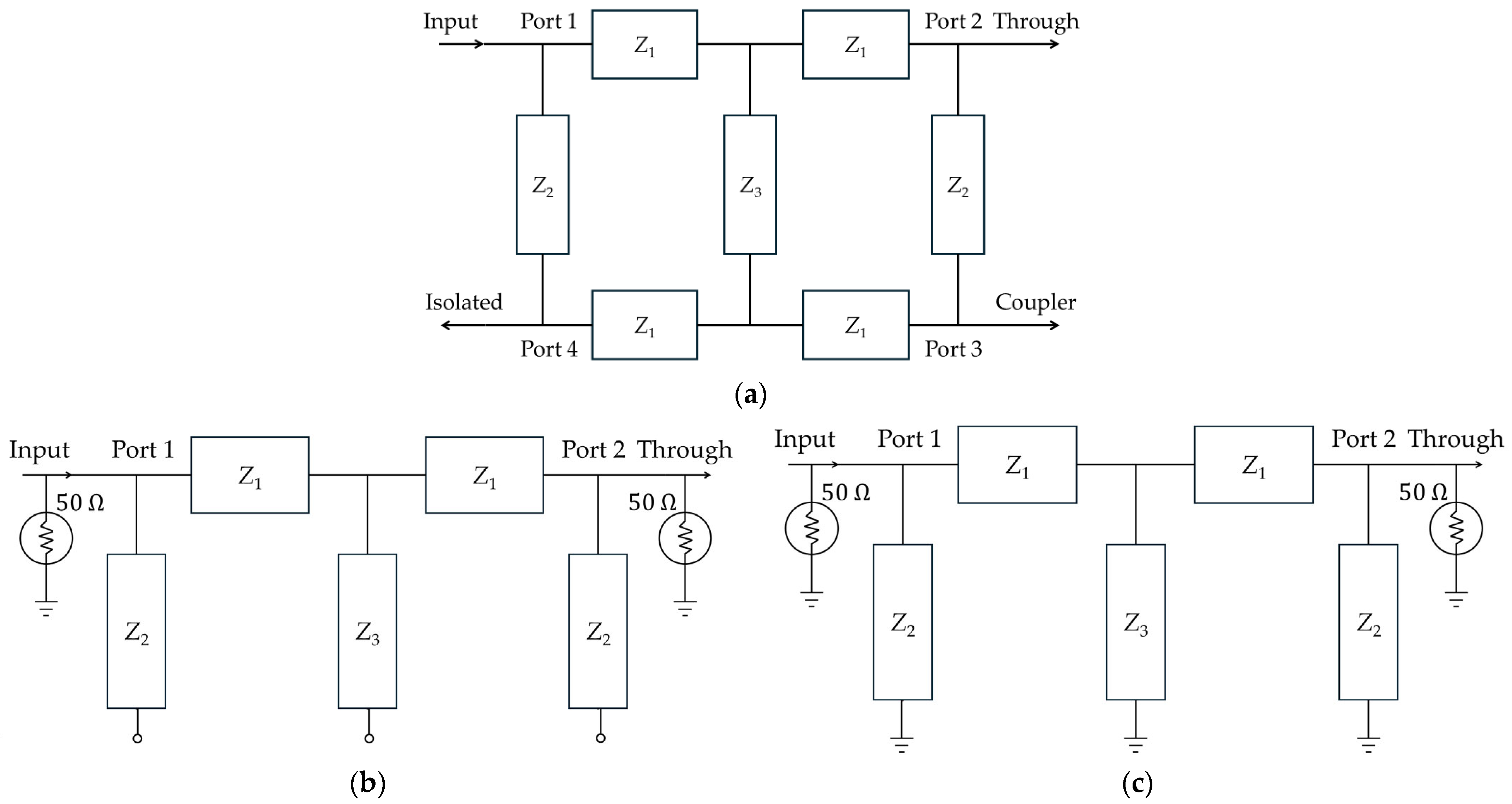
Conventional microstrip branch-line couplers are inherently limited by a relatively narrow bandwidth due to the strict quarter-wavelength requirement of the transmission lines. To overcome this and achieve ultra-wideband circular polarization performance, a two-section branch-line coupler is employed. To effectively extend the operational band-width, the proposed two-stage coupler is analytically designed based on a Chebyshev impedance matching polynomial form that strictly matches both Port 1 and Port 2 [15]. Based on the theoretical synthesis of a 3 dB broadband branch-line coupler, the ideal characteristic impedances are required to be , , and . The equivalent quasi-static Pi-network lumped elements (series inductance and shunt capacitance ) required to synthesize these transmission lines at the center frequency of 3.5 GHz are calculated and comprehensively summarized in Table 1. The mathematical design strictly requires the outer branches to have an exceptionally high characteristic impedance of approximately , while maintaining at the terminal ports. The complete four-port equivalent circuit of the proposed coupler is illustrated in Figure 1a.
Table 1.
Theoretical parameters and equivalent lumped elements of the two-stage branch-line coupler at 3.5 GHz.
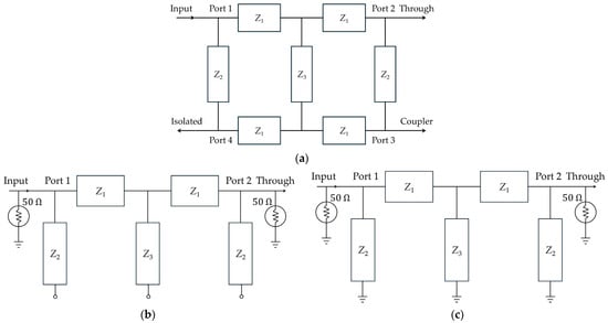
Figure 1.
Equivalent circuit models of the proposed DGS-enhanced two-stage branch-line coupler: (a) full four-port schematic, (b) even-mode half-circuit with open-ended stubs, and (c) odd-mode half-circuit with short-ended stubs.
The theoretical performance of this symmetrical structure is rigorously evaluated us-ing even–odd mode analysis [16]. By decomposing the excitation of the four-port network along the plane of symmetry, the structure is reduced to even (in-phase, magnetic wall) and odd (out-of-phase, electric wall) two-port half-circuits, as illustrated in Figure 1b,c. Mathematically, the overall ABCD parameters for the even-mode () and odd-mode () half-circuits are calculated by multiplying the cascaded transmission matrices of the individual series and shunt segments. According to the half-circuit models, the total matrices can be expressed as:
For the even-mode excitation, the symmetry plane acts as a magnetic wall, rendering the center of the shunt stubs as open circuits. Thus, the shunt matrices for and are given by:
Conversely, for the odd-mode excitation, the symmetry plane acts as an electric wall, creating short circuits. The shunt matrices are given by:
By substituting the expanded ABCD parameters from these cascaded matrices into the standard conversion formulas, the reflection and transmission coefficients can be determined as follows:
Consequently, by applying the principle of superposition, the overall S-parameters of the two-stage coupler are then reconstructed as:
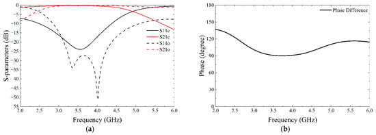
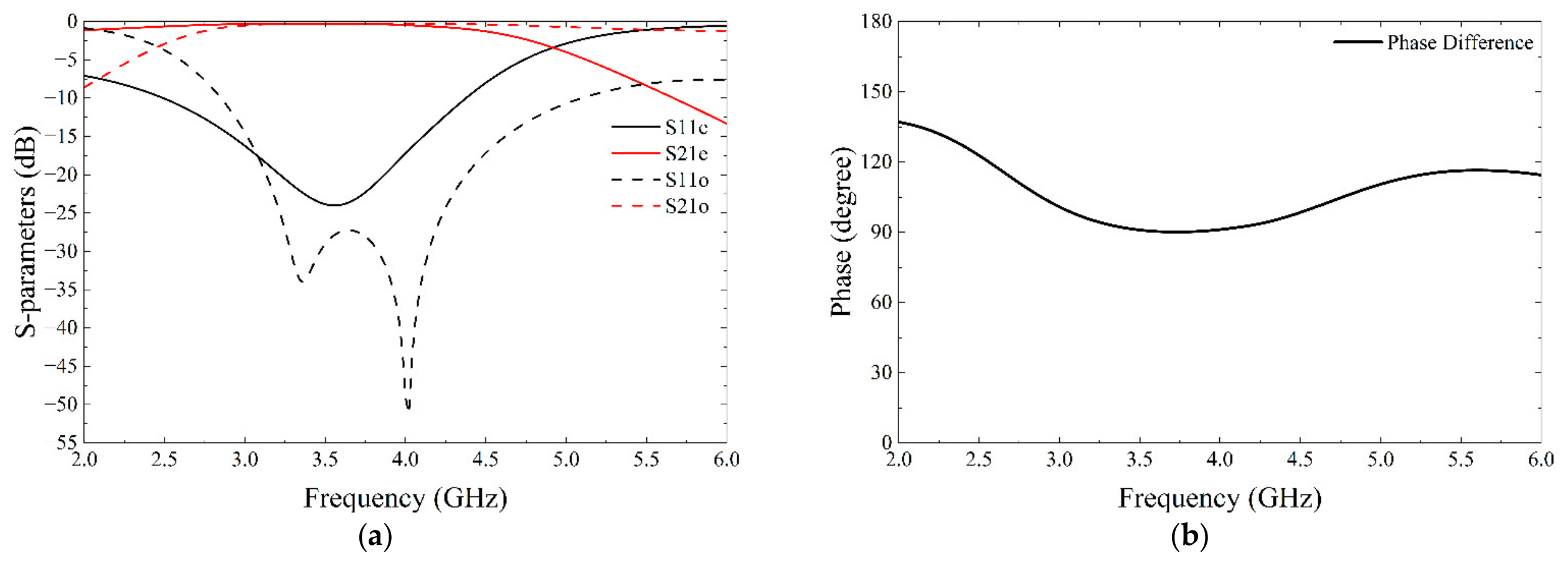
By plotting , , , and , the exact cancelation of reflections at the center frequency and the phase quadrature required for the CP generation are validated.
The operational bandwidth is explicitly validated from the magnitude responses. From Figure 2, the reflection coefficient consists of and , which maintain a −10 dB bandwidth across 2.60–4.35 GHz and 2.90–5.15 GHz, respectively. Therefore, the overall achieves a common wide bandwidth of 1.45 GHz (spanning from 2.90 to 4.35 GHz). The transmission coefficient consists of and , which exhibit a −4 dB bandwidth spanning 2.00–4.90 GHz and 2.65–6.00 GHz, respectively. Consequently, provides an effective overlapping bandwidth of 2.25 GHz.
Figure 2.
Simulated (a) magnitude responses and (b) phase difference in the even- and odd-mode half-circuits.
As previously analyzed, the mathematical design of the two-stage branch-line coupler strictly requires the outer branches to exhibit a high characteristic impedance () of approximately . Physically, this translates to extremely narrow microstrip traces that are severely limited by standard fabrication tolerances.
To study the effect of manufacturing errors, deviation of the trace by the maximum and minimum tolerance were used. In this work, Rogers 4350B with a dielectric constant of 3.48, substrate thickness of 0.762 mm, copper thickness of 0.035 mm was used. The regular trace width of microstrip line is about 0.22 mm. The simulation of a transmission line with , is studied.
From the ABCD matrix simulation, the characteristic impedance () and the electrical length () of the line can be extracted directly [17]:
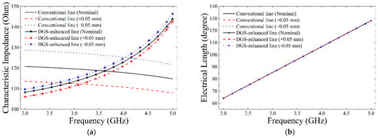
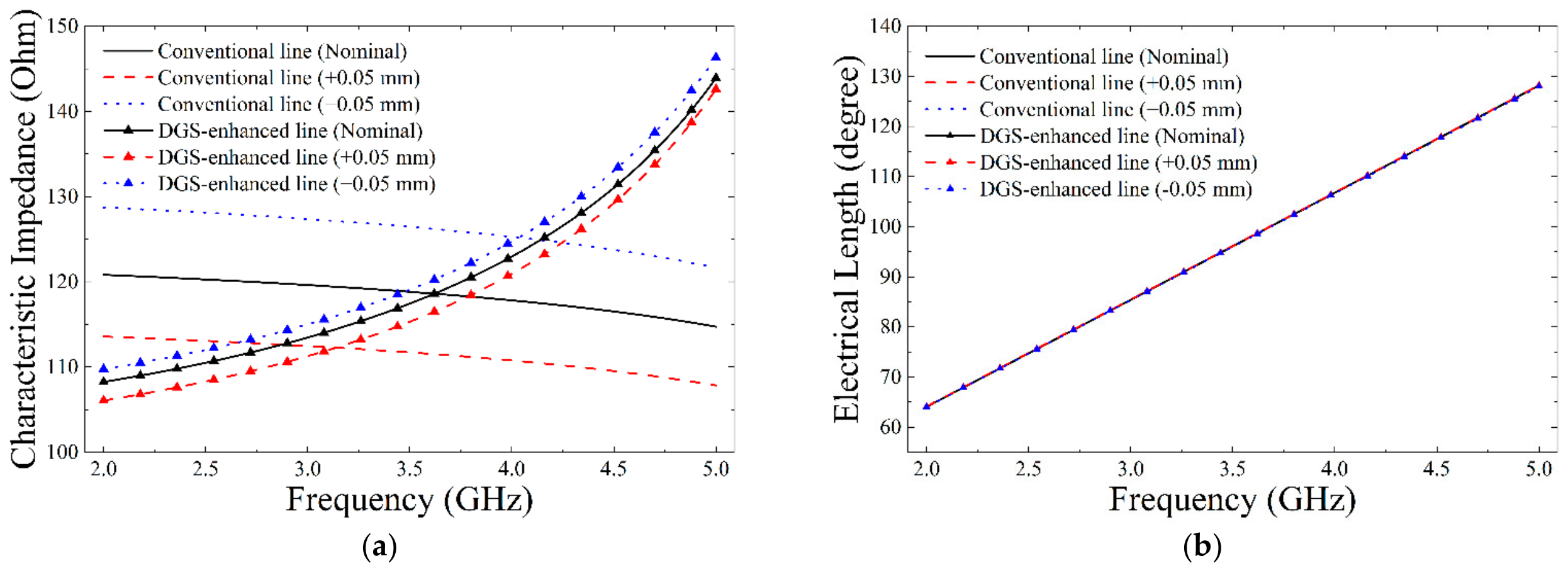
With the maximum and minimum deviation, the characteristic impedance varied as much as 6.7%, as shown in Figure 3, even though the electrical lengths remain relatively stable. Therefore, the deviation from manufacturing drastically changes the transmission line properties, which implies a worsened branch-line performance. To overcome this vulnerability, the proposed DGS-enhanced transmission lines were studied.
Figure 3.
Extracted equivalent transmission line parameters of a conventional line under fabrication tolerances: (a) characteristic impedance () and (b) electrical length (). The “Nominal” lines represent the ideal design dimensions, while the “+0.05 mm” and “−0.05 mm” lines indicate the upper and lower limits of the fabrication tolerances applied to the trace widths for both the conventional and DGS-enhanced transmission lines.
2.2. Equivalent Circuit Model of DGS
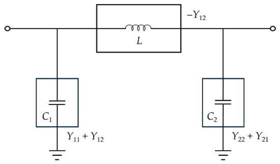
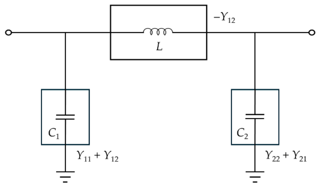
For a regular microstrip line, increasing the trace width results in a lower characteristic impedance. To overcome the fabrication bottlenecks of high-impedance lines or narrow traces, a Defected Ground Structure (DGS) is utilized. The fundamental principle of the DGS can be accurately modeled using a quasi-static Pi-network equivalent circuit. To observe the physical impact of the DGS on the transmission line, the simulated scattering parameters (S-parameters) are mathematically converted to admittance parameters (Y-parameters) using the quasi-static -network equivalent circuit model as shown in Figure 4.
Figure 4.
The quasi-static -network equivalent circuit model of the proposed Defected Ground Structure (DGS), where the lumped components () are mapped directly to the two-port Y-parameters.
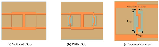
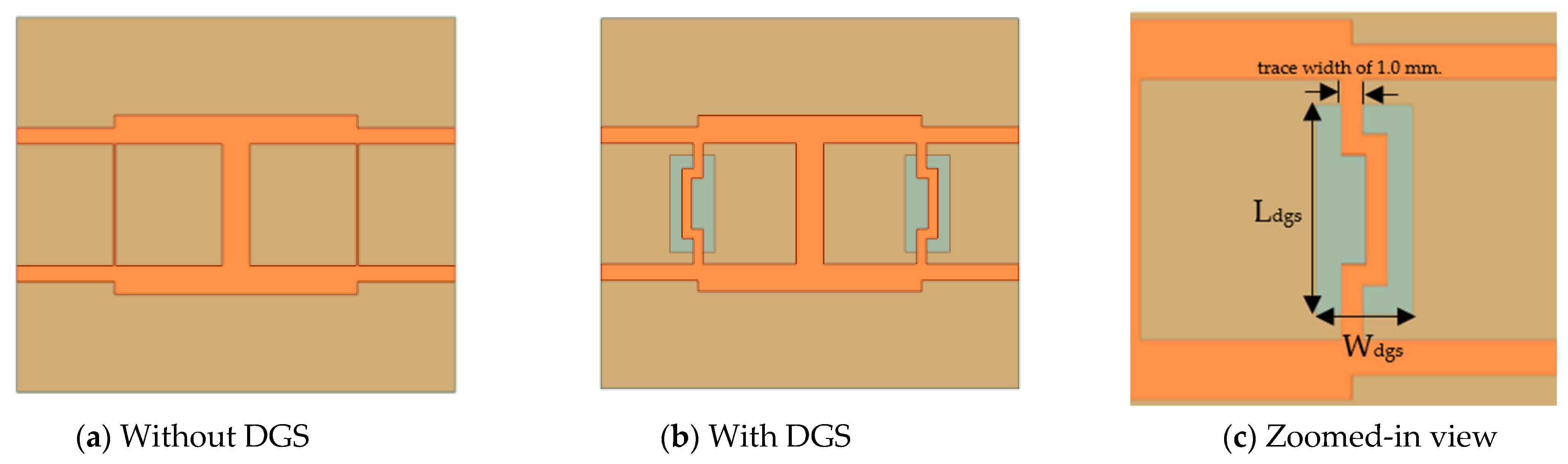
In this design, the trace width over the DGS is targeted to be widened to 1.0 mm. An extended parametric study on the DGS width () is introduced. Figure 5 shows the coupler structure with and without DGS. The variation in directly affects the characteristic impedance tuning process. Furthermore, the extracted and graphs for both the conventional narrow line and the proposed DGS-enhanced wide line demonstrate that the properties are strictly preserved. Fundamentally, etching the defect on the ground plane forces the return current to follow a longer detour path, which significantly increases the distributed series inductance (). This allows the physical width of the trace to be expanded, thereby increasing the shunt capacitance () to perfectly balance the characteristic impedance ratio () at .
Figure 5.
Detailed geometry of the proposed Defected Ground Structure (DGS): (a) conventional layout without DGS, (b) overall layout with DGS, and (c) zoomed-in view of the DGS-enhanced transmission line with a fixed widened trace width of 1.0 mm.
To thoroughly investigate the physical mechanism of the DGS, a parametric study on the defected slot dimensions is conducted. First, the variation in the slot length () directly influences the distributed equivalent series inductance of the transmission line. An inadequate slot length provides insufficient inductance, whereas an excessive length introduces severe impedance mismatch, behaving similarly to a bandstop filter.
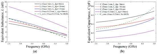
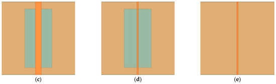
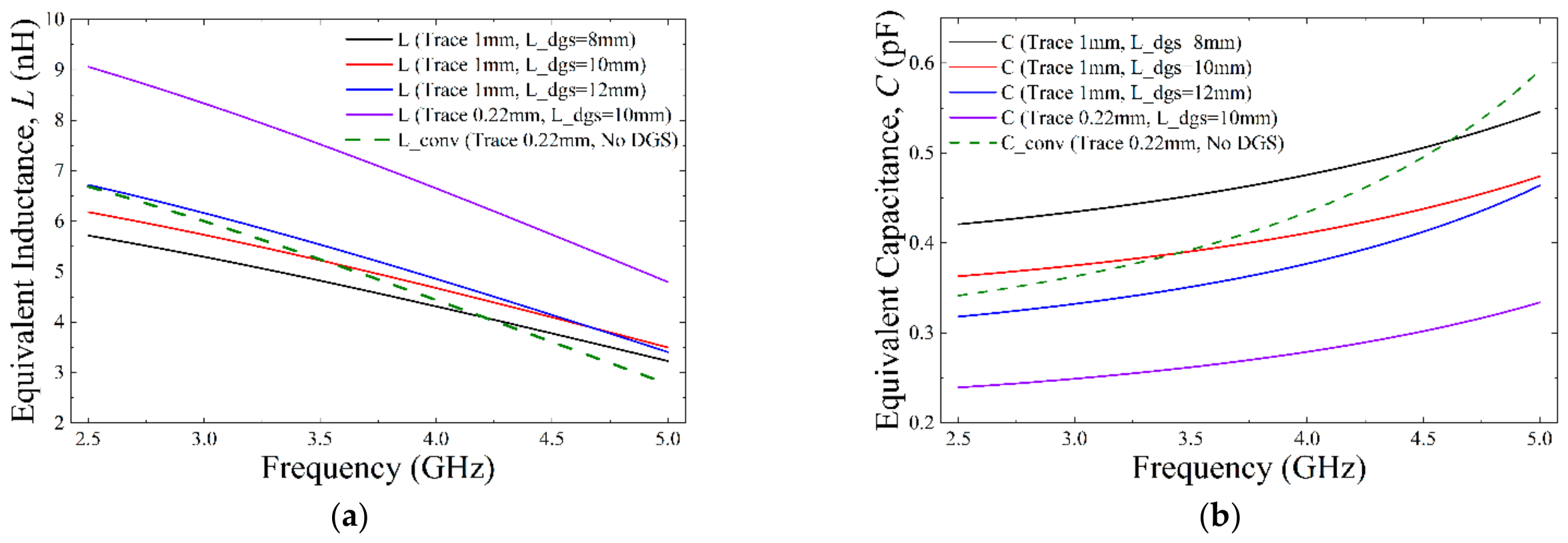
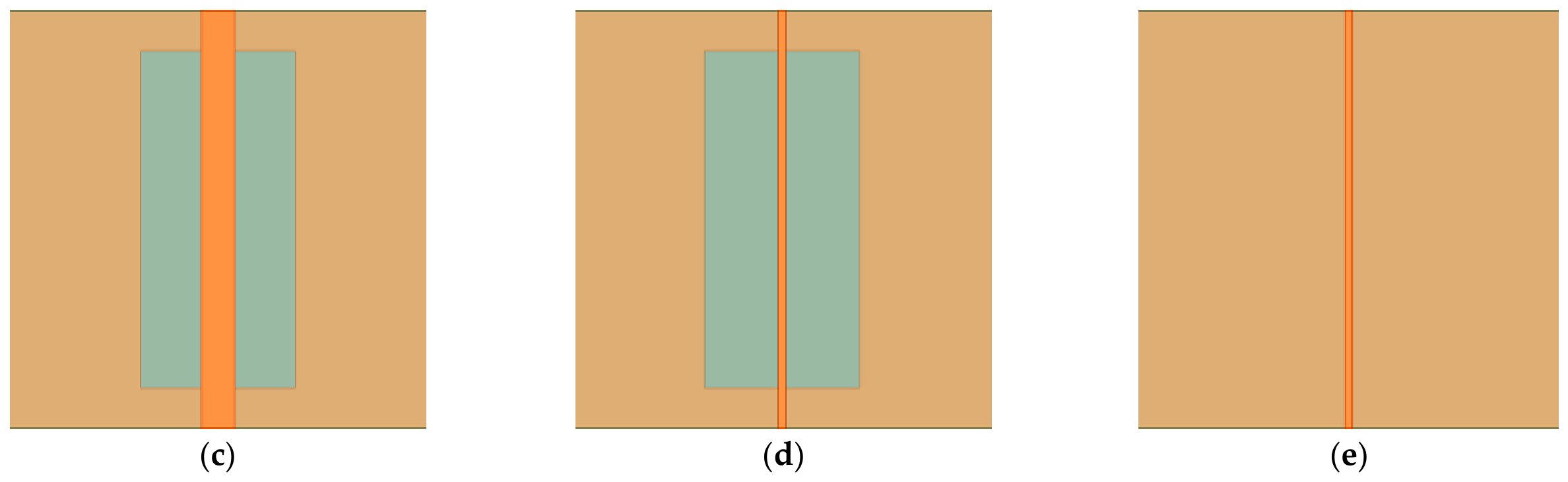
To investigate the physical mechanism of the DGS, a parametric study on the defected slot dimensions is conducted. As illustrated in Figure 6a,b, the variation in the slot length () directly influences the equivalent series inductance () and shunt capacitance () of the transmission line. To establish a clear physical baseline and explicitly illustrate the geometric modifications, the structural layouts of three comparative cases are provided in Figure 6c–e. As explicitly shown at the center frequency of 3.5 GHz, the proposed 1.0 mm wide trace with a 10 mm DGS (Figure 6c) effectively exhibits the nearly identical and values as the practically unmanufacturable 0.22 mm narrow line without DGS (Figure 6e). From the figure, the DGS increases the inductance (), allowing the trace width to be widened while maintaining approximately the same and values to achieve the desired characteristic impedance . Furthermore, compared to the highly dispersive conventional line, the and curves of the proposed DGS-enhanced line exhibit significantly flatter slopes across the operating band. This dispersion compensation effectively stabilizes the characteristic impedance over a broader frequency range, which fundamentally explains the bandwidth enhancement mechanism of the overall coupler.
Figure 6.
Extracted equivalent circuit parameters of the transmission lines compared with a conventional narrow line, alongside their corresponding structural layouts: (a) equivalent series inductance (), (b) equivalent shunt capacitance (), (c) layout of the proposed 1.0 mm widened trace with DGS, (d) layout of the 0.22 mm narrow trace with DGS, and (e) layout of the conventional 0.22 mm narrow trace without DGS.
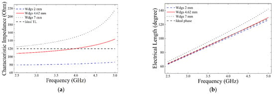
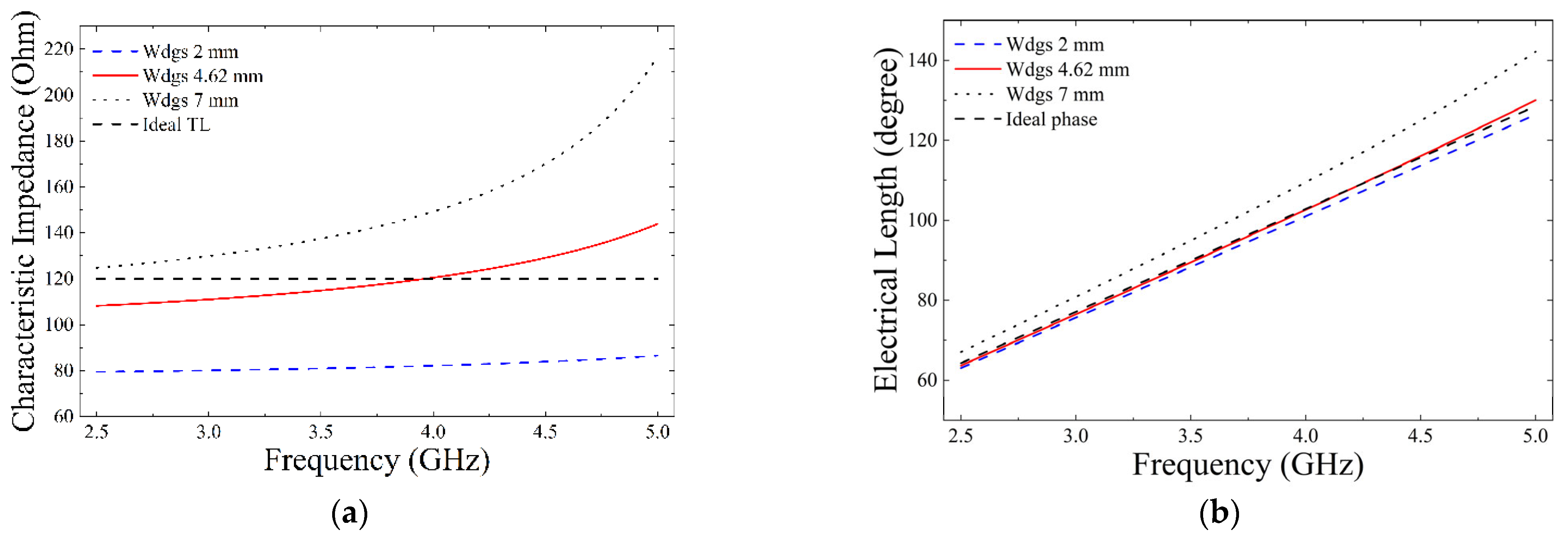
The extracted graphs clearly demonstrate that modifying allows precise control over the line’s impedance. As required by the two-stage coupler design, the targeted ideal transmission line (TL) must strictly exhibit a characteristic impedance of and an electrical length of at the center frequency of 3.5 GHz. As shown in Figure 7, the optimal dimensions of mm and mm are selected. These specific dimensions effectively compensate for the parasitic capacitance, firmly securing the required and properties exactly at 3.5 GHz. Furthermore, as observed from the extracted impedance curve in Figure 7a, the characteristic impedance of the proposed DGS-enhanced line smoothly varies between and across the broad frequency range of 2.5 GHz to 4.2 GHz. This explicitly demonstrates that the impedance deviation strictly remains within an acceptable error margin from the ideal nominal value, thereby maintaining stable wideband coupler performance. The selected values are also studied with manufacturing variation. The trace width values of were simulated. The results are shown in Figure 3. From the figure, the DGS reduces the variation in the characteristic impedance. The maximum variation is only 1.7% from the nominal value. Despite the steeper impedance variation in Defected Ground Structure (DGS) lines compared to conventional microstrip lines, a wideband coupler design can be achieved through careful selection of the operating frequency range and circuit optimization.
Figure 7.
Extracted equivalent transmission line parameters of 120 Ω lines (a) characteristic impedance () and (b) electrical length ().
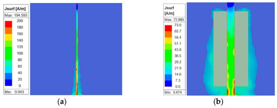
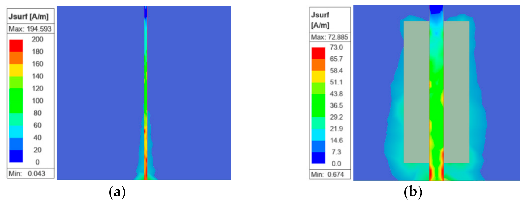
To explicitly visualize the current-blocking effect of the proposed DGS, the simulated surface current distributions on both the conventional and the DGS-enhanced transmission lines are compared in Figure 8. As observed in Figure 8a, the surface current on the conventional microstrip line flows straightforwardly along the center of the narrow trace. However, when the DGS is introduced (Figure 8b), the etched rectangular slot on the ground plane acts as a physical barrier. This current-blocking effect strongly forces the current to distribute and detour around the slot edges. The lengthened current path visually confirms the physical generation of the additional distributed series inductance, which firmly supports the simulation results in Figure 6a.
Figure 8.
Simulated surface current distributions illustrating the current-blocking effect: (a) conventional microstrip line and (b) proposed DGS-enhanced transmission line. The different colors represent the varying intensity of the surface current density, with red indicating the highest intensity and blue the lowest.
2.3. Stacked Patch Antenna Design
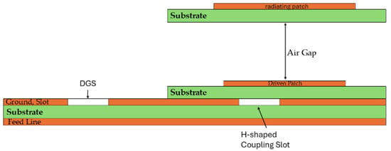
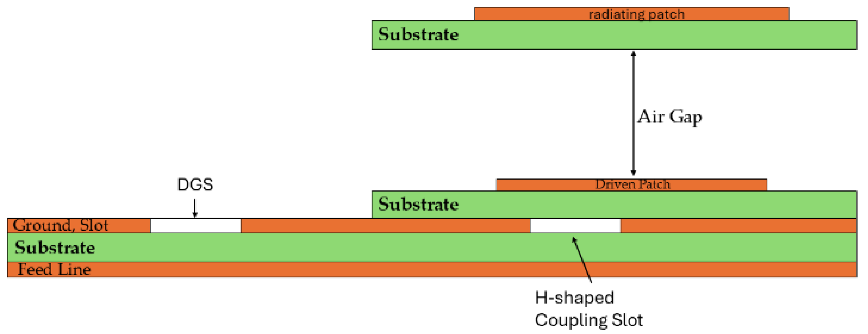
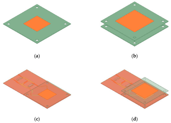
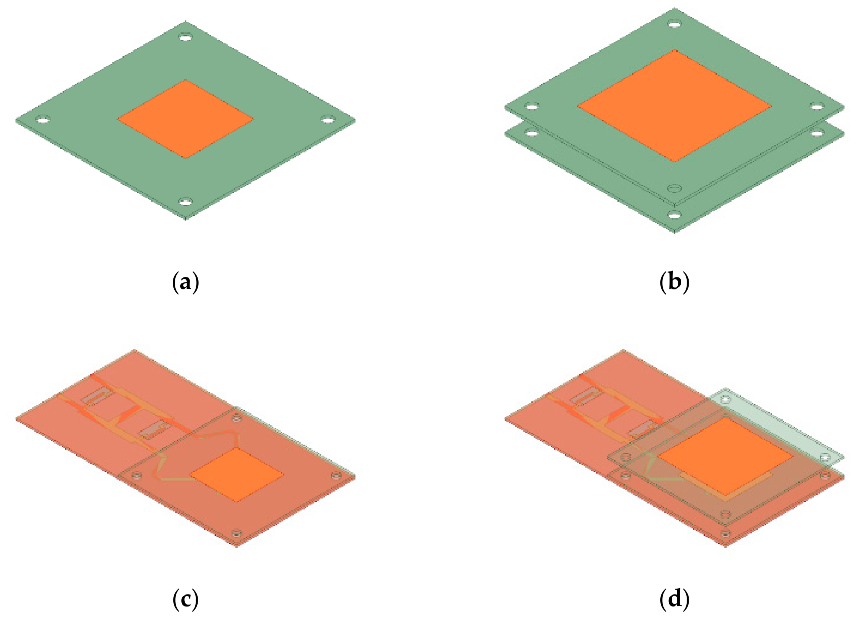
To explicitly highlight the necessity of the proposed structure as shown in Figure 9, the radiating element is analyzed across four evolutionary configurations: (1) a standalone single patch antenna without the feed network, (2) a standalone stacked patch antenna without the feed network, (3) a single patch integrated with the two-stage branch-line coupler, and (4) the proposed stacked patch integrated with the DGS-enhanced two-stage branch-line coupler. The patch antenna has evolved from the conventional single patch to the stacked patch antenna. Figure 10 compares the conventional design (Figure 10a,c) with the stacked configuration (Figure 10b,e).
Figure 9.
Cross-sectional view of the proposed stacked patch antenna illustrating the aperture-coupled mechanism via the H-shaped slot.
Figure 10.
Evolution of the proposed antenna design: (a) Configuration 1: standalone single patch, (b) Configuration 2: standalone stacked patch, (c) Configuration 3: single patch with two-stage branch-line coupler, and (d) Configuration 4: proposed stacked patch with DGS-enhanced two-stage branch-line coupler.
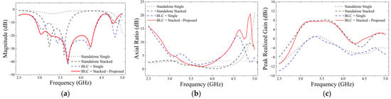
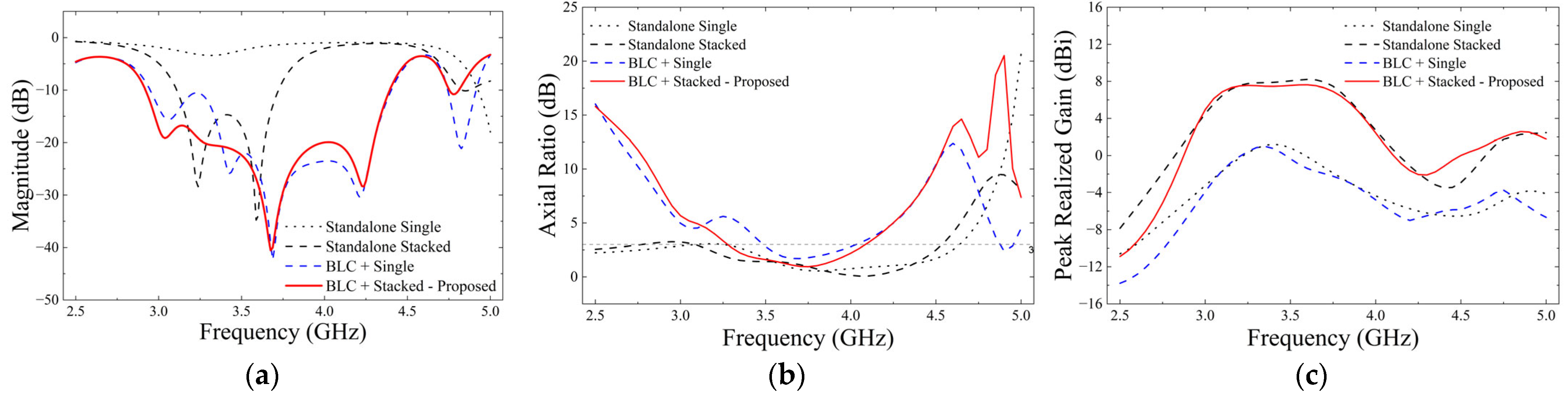
As demonstrated in the reflection coefficient () comparisons in Figure 11a, the standalone single patch (Configuration 1) inherently yields a narrow impedance bandwidth with a single deep resonance. Introducing a parasitic patch suspended by an air gap (Configuration 2) drastically broadens the bandwidth by exciting an additional resonant mode. However, directly integrating the narrow-band single patch with the dual-feed branch-line coupler (Configuration 3) leads to an unstable impedance mismatch. In this case, a lower peak realized gain can be observed as shown in Figure 11c.
Figure 11.
Simulated comparison of the four antenna configurations: (a) reflection coefficient (|S11|), (b) axial ratio, and (c) peak realized gain. The legend terms denote the evolutionary configurations: “Standalone Single” (single patch without feed network), “Standalone Stacked” (stacked patch without feed network), “BLC + Single” (single patch with branch-line coupler), and “BLC + Stacked (Proposed)” (proposed stacked patch with DGS-enhanced branch-line coupler).
In contrast, the proposed configuration (Configuration 4), which integrates the broadband stacked patches with the DGS-enhanced branch-line coupler, provides broad bandwidth with higher peak realized gain. The overall structure maintains an ultra-wide active impedance bandwidth () of 41.6%, covering from 2.92 to 4.37 GHz. The broad overlapping resonance strictly ensures that the input power is efficiently coupled to the radiating elements with the maximum peak realized gain of 7.54 dBi at 3.5 GHz. Furthermore, as illustrated in Figure 11b, the stacked configuration yields 3 dB axial ratio bandwidth from 3.26 to 4.07 GHz. Furthermore, to explicitly quantify the effect of the aperture-coupled mechanism and the large air gap, the simulated radiation efficiencies at the center frequency of 3.5 GHz for the four evolutionary configurations were evaluated. Due to severe impedance mismatch at 3.5 GHz, the standalone single patch (Configuration 1) yields an efficiency of only 57%. When this mismatched patch is directly integrated with the coupler (Configuration 3), the reflected power is heavily dissipated at the isolation resistor, dropping the overall efficiency to 46%. Conversely, the introduction of the parasitic patch and the air gap (Configuration 2) effectively matches the antenna, boosting the efficiency to 93%. Ultimately, the final proposed structure integrated with the DGS-enhanced coupler (Configuration 4) successfully maintains a high simulated radiation efficiency of 88%. This explicitly confirms that the wideband air gap mechanism does not degrade the efficiency; rather, it is crucial for maximizing power delivery and preventing resistor dissipation.
2.4. Overall Antenna Design and Configuration Summary
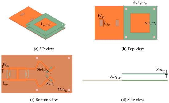
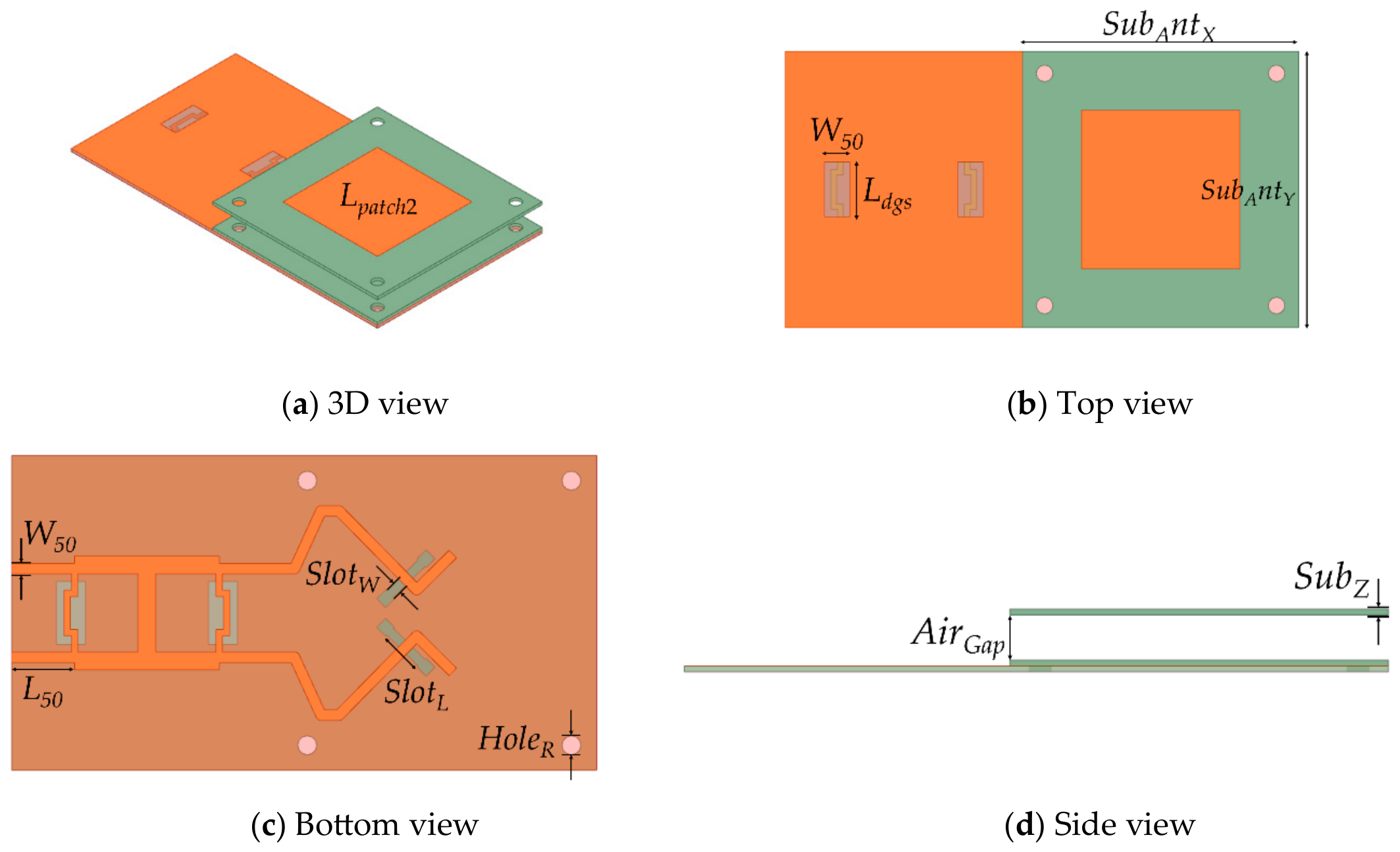
Based on the sequential design process described above, the final configuration of the proposed wideband CP antenna consists of three main layers: the DGS-enhanced feed network at the bottom, the driven patch in the middle, and the radiating patch separated by an air gap at the top. The overall structure of the antenna is shown in Figure 12. As depicted in the geometric layout, the physically long high-impedance branches are intentionally bent into meander lines. This meandering technique is adopted strictly for miniaturization, effectively compressing the overall footprint of the two-stage coupler to ensure a compact antenna profile without altering the required electrical phase delay.
Figure 12.
Geometry of the proposed antenna: (a) 3D view, (b) top view, (c) bottom view, and (d) side view.
To guarantee a highly precise physical alignment prior to the actual fabrication, four alignment holes were strategically designed at the corners of the substrates. Non-conductive nylon screws and standoffs are utilized to firmly assemble the structure. The air gap height can be fine-tuned by sliding the substrates along the screws, and a Vernier caliper was strictly used to measure and calibrate the gap to exactly 5.96 mm. This mechanical alignment method effectively prevents any performance degradation caused by layer misalignment.
The optimized physical dimensions of the overall structure are summarized in Table 2. With proper alignment, the integration of the DGS-enhanced branch-line coupler perfectly complements the aperture-coupled stacked patches.
Table 2.
Dimensions of the proposed antenna parameters.
3. Results and Discussion
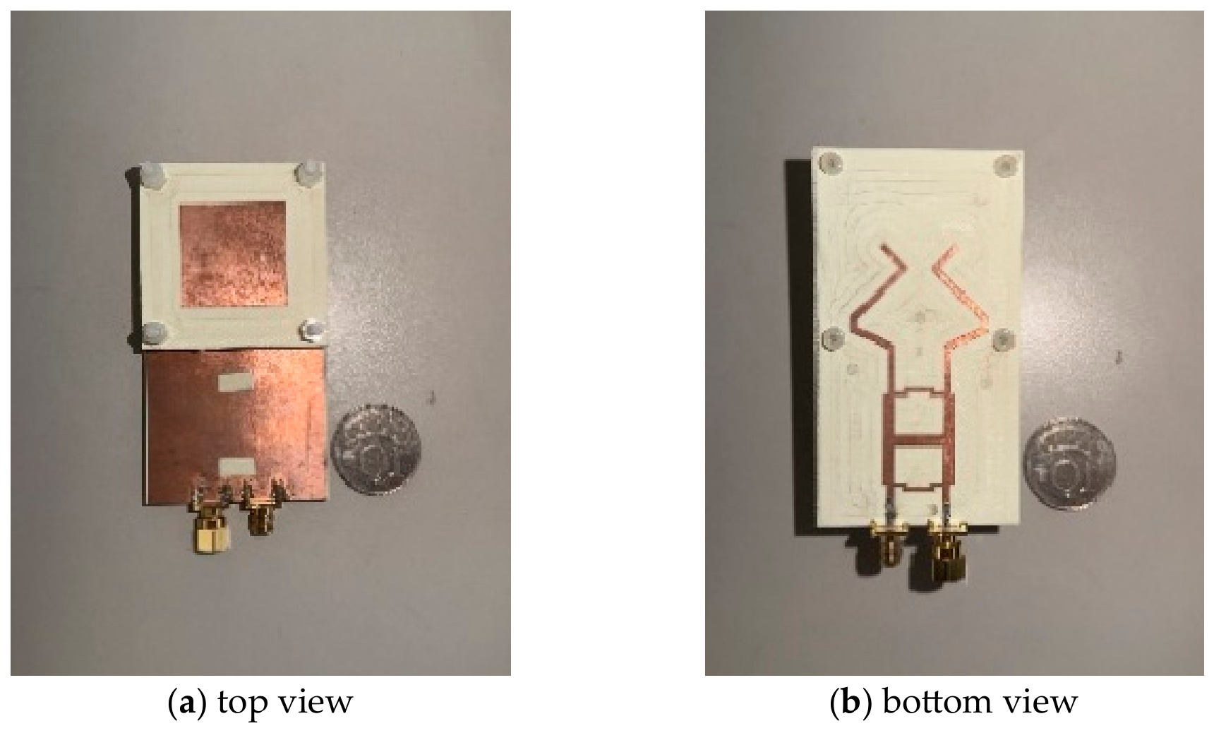
To validate the design concept, a prototype of the proposed antenna was fabricated and measured. The prototype is shown in Figure 13. During the experimental validation in the anechoic chamber, the proposed integrated antenna was measured using a single-port configuration. To accurately emulate the real-world operational conditions of a dual-feed CP antenna, the isolated port of the two-stage branch-line coupler was strictly terminated with a standard 50 Ω broadband matched load. This physical termination is critical to fully absorb any unbalanced reflected power originating from the slight mismatches of the orthogonal modes, thereby preventing multiple reflections and standing waves within the feed network. The input return loss () was then recorded using a Vector Network Analyzer (VNA, Keysight PNA N5225B, Keysight Technologies, Santa Rosa, CA, USA), representing the true active reflection coefficient of the entire antenna system.
Figure 13.
Photographs of the fabricated antenna prototype: (a) top view and (b) bottom view.
The measurement results show an outstanding agreement with the full-wave simulation, confirming the robustness of the DGS technique against manufacturing errors. As illustrated in Figure 14, the antenna exhibits a measured impedance bandwidth of 41.6% (2.92–4.37 GHz). The axial ratio performance is evaluated via numerical simulation due to measurement setup constraints, yielding a 3 dB AR bandwidth from 3.26 GHz to 4.07 GHz. The operational CP bandwidth is defined by the overlap between the reflection coefficient and the 3 dB axial ratio bandwidth. Furthermore, the antenna delivers a stable broadside radiation pattern with a simulated peak realized gain of 7.54 dBi at 3.5 GHz as indicated in Figure 15 and Figure 16. To comprehensively validate the dual-CP performance, the fabricated prototype was measured in a Compact Antenna Test Range (CATR) chamber. The measured peak realized gains for exciting Port 1 and Port 2 are approximately 7.54 dBi and 7.18 dBi at 3.5 GHz, respectively. This close agreement firmly confirms the highly symmetrical performance of both polarization states. In addition, the measured radiation efficiency of the proposed antenna at the center frequency of 3.5 GHz is 82.2%, which agrees well with the simulated efficiency of 88%. This effectively validates that the aperture-coupled mechanism with the large air gap maximizes radiation without excessive power dissipation.
Figure 14.
Simulated and measured reflection coefficients () of the proposed antenna. The solid line refers to the simulated results while the dash line refers to the measured results.
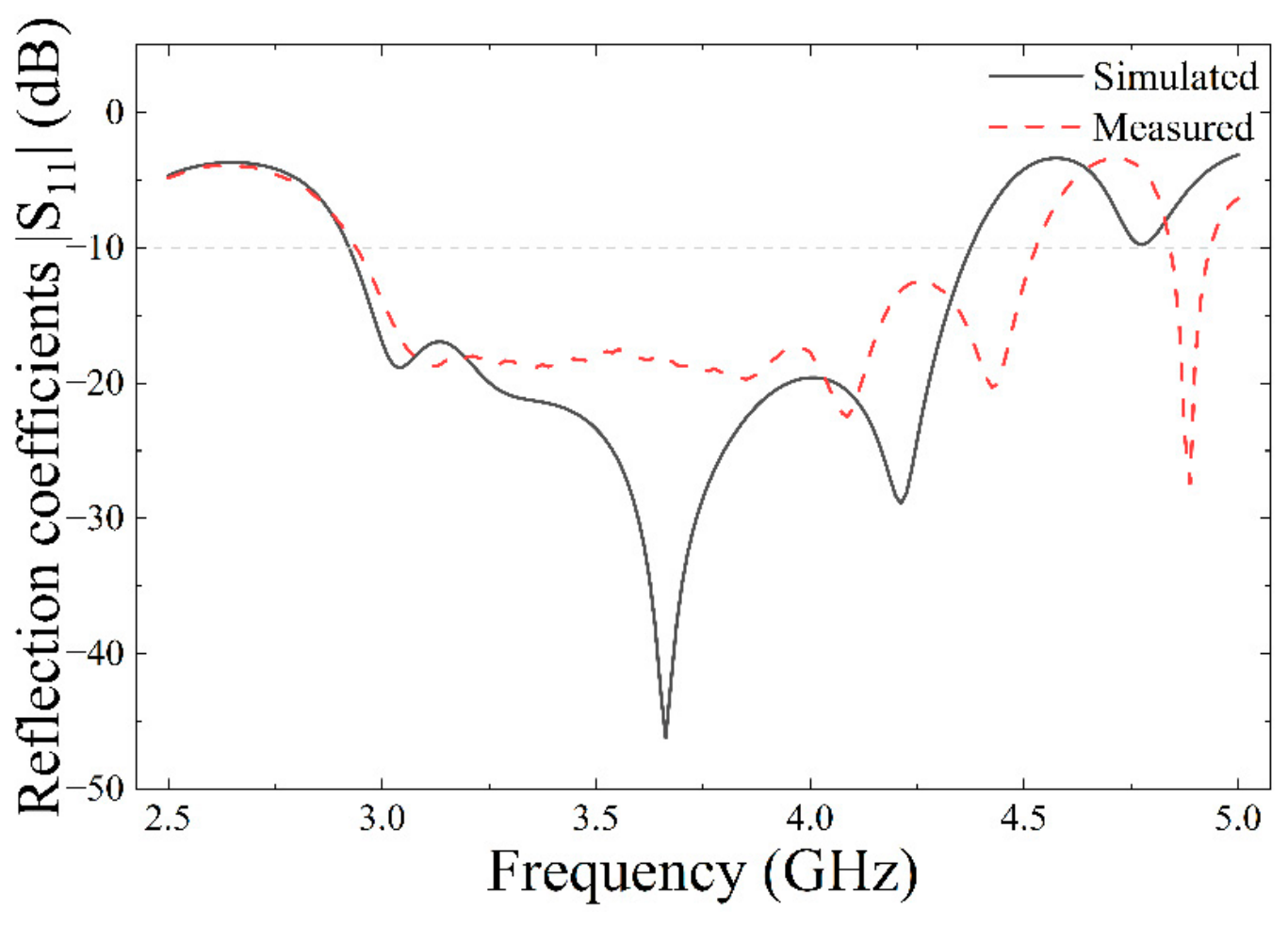
Figure 15.
Simulated and measured peak realized gain versus frequency. The solid line refers to the simulated results while the dash line refers to the measured results.
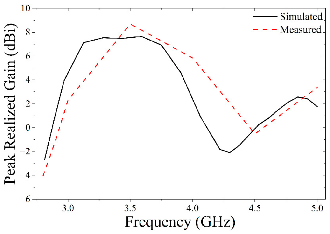
Figure 16.
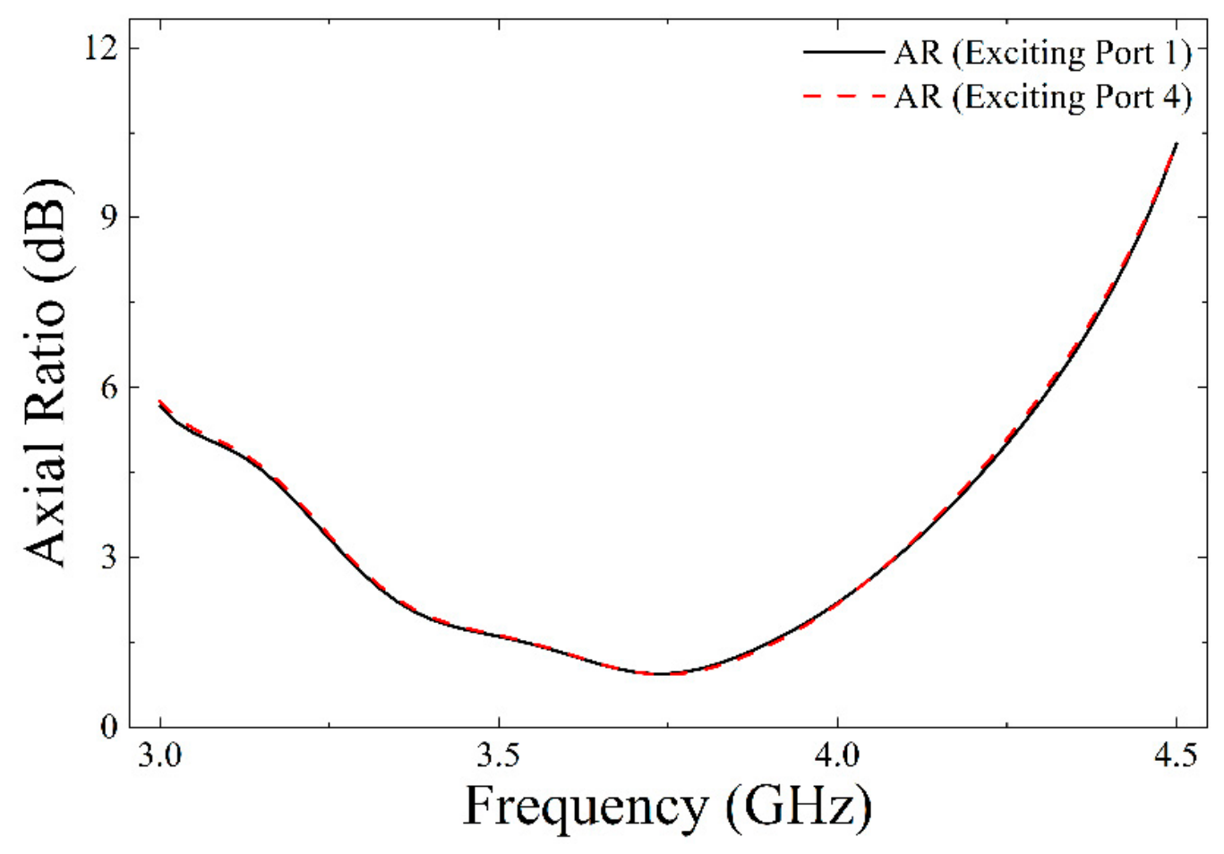
Radiation patterns at 3.5 GHz for the azimuth angle of and planes: (a) simulated and measured co-polarization, and (b) simulated co-polarization and cross-polarization. The solid lines refer to the simulated results while the dash lines refer to the measured results. To verify the operating principle of the DGS-enhanced feed network, the two-stage branch-line coupler was simulated independently. The simulated S-parameters show that the input power from Port 1 is equally divided into the through and coupled ports with magnitudes of approximately −3 dB across the operating band as shown in Figure 17. Furthermore, an exact phase difference between the two output ports is maintained around the center frequency of 3.5 GHz, confirming the capability of the proposed coupler to excite the orthogonal modes required for CP radiation as shown in Figure 18. Specifically, the polarization switching is achieved simply by changing the excitation port. When the RF signal is fed to Port 1, the coupler provides a phase difference, resulting in Right-Hand Circular Polarization (RHCP). Conversely, when the signal is switched to Port 4, a phase difference is generated, strictly yielding Left-Hand Circular Polarization (LHCP). The simulated surface current distributions at 3.5 GHz for different phases are illustrated in Figure 19. As demonstrated in Figure 20, the simulated axial ratio comparison for both excitation scenarios confirms that the strictly symmetrical property of the feed network ensures the antenna delivers identical ultra-wideband CP performance for both polarization states.
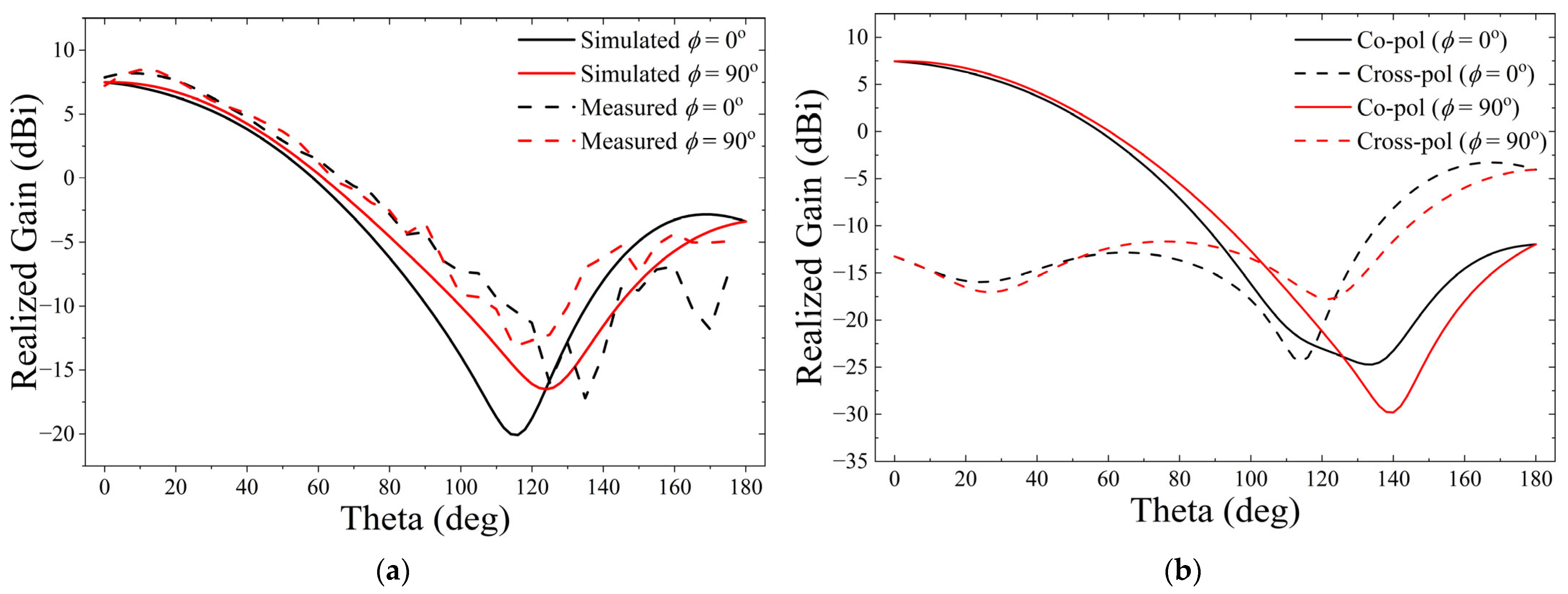
Figure 17.
Simulated S-parameters of the proposed DGS-enhanced two-stage coupler.
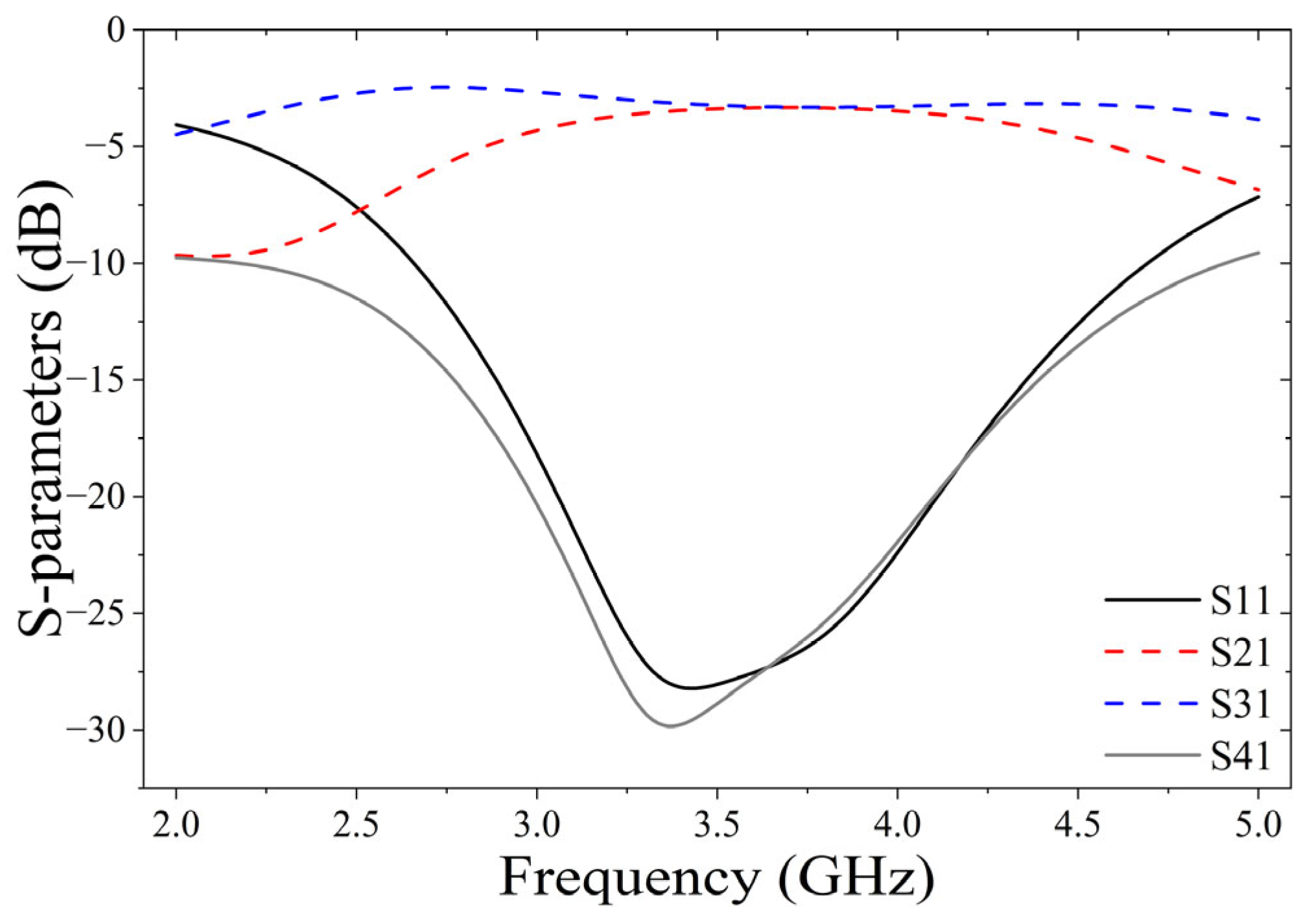
Figure 18.
Simulated phase difference between the through and coupled ports of the proposed coupler.
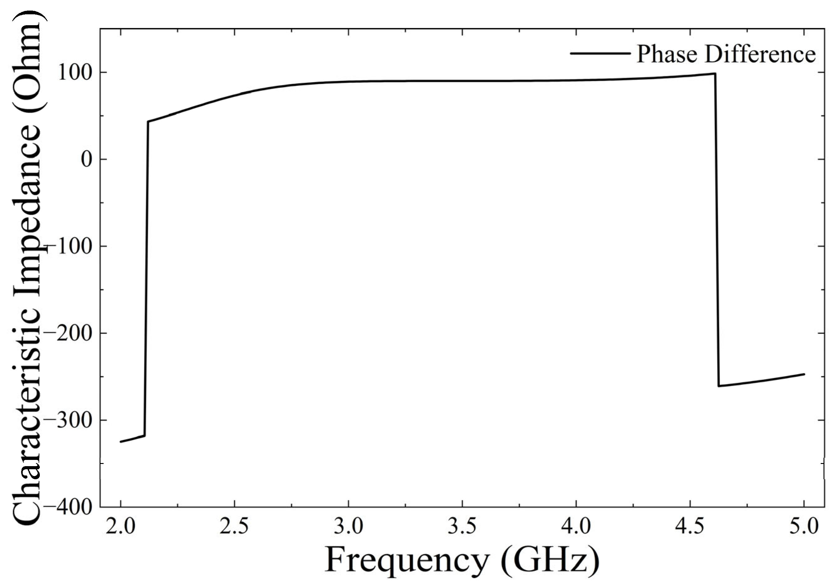
Figure 19.
Simulated surface current distributions on the radiating patch at 3.5 GHz for different phases: (a) , (b) , (c) , and (d) . The large red arrows represent the average direction of the surface current, which rotates over time.
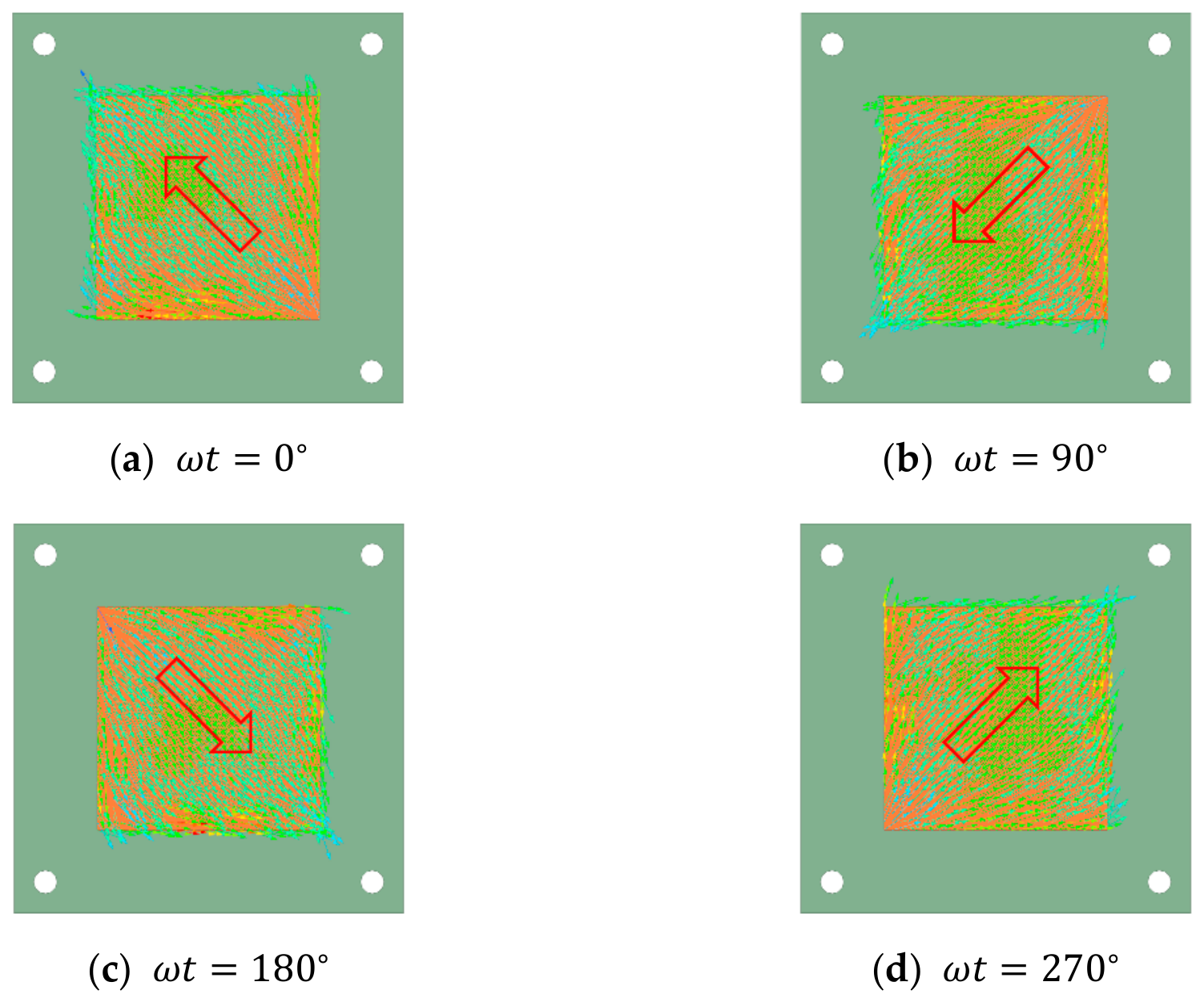
Figure 20.
Simulated axial ratio comparison between exciting Port 1 and Port 4 for dual circular polarization. The horizontal gray dotted line indicates the 3-dB reference level for the axial ratio.
To ensure the radiation characteristics remain stable across the operating band, Figure 16a illustrates the simulated and measured radiation patterns at the center frequency of 3.5 GHz for both the and planes. The patterns remain highly stable and symmetrical, maintaining a broadside directional radiation. Moreover, to comprehensively evaluate the circular polarization purity, the simulated cross-polarization (LHCP) levels are plotted alongside the primary co-polarization (RHCP) levels in Figure 16b. As depicted, the cross-polarization is significantly suppressed by more than 20 dB compared to the co-polarization at the broadside direction () for both orthogonal planes. This high cross-polarization discrimination (CPD) explicitly confirms the excellent CP performance of the proposed antenna.
Table 3 presents a comparison between the proposed antenna and state-of-the-art designs reported in the literature. Compared to existing dual-feed stacked antennas, this single-element design achieves an optimal balance among wide bandwidth, high gain, and manufacturing practicality. Specifically, it features a measured −10dB impedance bandwidth of 41.6% (2.92–4.37 GHz), a simulated 3 dB axial ratio bandwidth (ARBW) of 22.1% (3.26–4.07 GHz), and a peak gain of 7.54 dBi.
Table 3.
Comparison of the proposed antenna with other existing CP antennas.
4. Conclusions
A wideband circularly polarized (CP) stacked patch antenna utilizing a DGS-enhanced two-stage coupler is presented and validated. By integrating Defected Ground Structures (DGSs), the physical fabrication constraints of microscopic high-impedance lines are successfully overcome. Operating in the 5G Sub-6 GHz band, the proposed single-element antenna achieves a broad impedance bandwidth of 41.6%, a CP bandwidth of 23.14%, and a peak gain of 7.54 dBi. Measured results show excellent agreement with simulations, confirming its low-profile characteristics and fabrication feasibility. This design offers a highly practical solution for modern wireless systems, including 5G CPE routers, autonomous vehicles, and drone communications.
Author Contributions
Conceptualization, P.M. and C.P.; Methodology, P.M.; Software, P.M. and C.P.; Validation, P.M., S.W. and C.P.; Writing—original draft preparation, P.M.; Writing—review and editing, S.W. and C.P.; Supervision, C.P. All authors have read and agreed to the published version of the manuscript.
Funding
This work was financially supported by College of Advanced Manufacturing Innovation, King Mongkut’s Institute of Technology Ladkrabang [grant number: AMI-RESERCH-02-2567-01M]. This work is also supported by National Taipei University of Technology-King Mongkut’s Institute of Technology Ladkrabang Joint Research Program (NTUT-KMITL No. NTUT-KMITL-113-02) and National Science and Technology Council under NSTC 113-2218-E-A49-020.
Data Availability Statement
Data will be made available on request.
Acknowledgments
The authors gratefully acknowledge the Wireless Communication Laboratory, Faculty of Engineering, Rajamangala University of Technology Thanyaburi, for providing the facilities for the fabrication and testing of this work.
Conflicts of Interest
The authors declare no conflicts of interest.
References
- Táboas, M.P.; Vera-Isasa, M.; García Sánchez, M. Self-interference suppression improvement by employing circular polarized antennas. Measurement 2017, 110, 53–59. [Google Scholar]
- Mohammed, A.H.; Alnahwi, F.M.; Al-Yasir, Y.I.A. A Circularly Polarized Microstrip Antenna with Dual Circular Polarization Using a 90° Hybrid Coupler and Proximity-Coupled Feeding for LTE 43 5G Applications. Appl. Sci. 2024, 14, 11877. [Google Scholar]
- Wen, L.; Zheng, S.Y.; Pan, Y.M.; Yin, Y. Design of a wideband dual-feed circularly polarized antenna for different axial ratio requirements. IEEE Antennas Wirel. Propag. Lett. 2021, 20, 88–92. [Google Scholar]
- Rowe, W.S.T.; Waterhouse, R.B. Investigation into the performance of proximity coupled stacked patches. IEEE Trans. Antennas Propag. 2006, 54, 1693–1698. [Google Scholar]
- El Yousfi, A.; Lamkaddem, A.; Abdalmalak, K.A.; Segovia-Vargas, D. A Broadband Circularly Polarized Single-Layer metasurface Antenna Using Characteristic-Mode Analysis. IEEE Trans. Antennas Propag. 2023, 71, 3114–3122. [Google Scholar]
- Jin, P.; Ziolkowski, R.W. Multi-frequency, linear and circular polarized, metamaterial-inspired, near-field resonant parasitic antennas. IEEE Trans. Antennas Propag. 2011, 59, 1446–1459. [Google Scholar]
- Alsuwayyeh, Y.; Vettikalladi, H.; Almoneef, T. A Low-Profile High Gain Circularly Polarized Metasurface Antenna for IoT Applications. Electronics 2026, 15, 822. [Google Scholar]
- Li, Z.; Liu, Y.; Zhao, M.; Zong, W.; He, S. A Wideband Circularly Polarized Metasurface Antenna with High Gain Using Char-acteristic Mode Analysis. Electronics 2025, 14, 2818. [Google Scholar]
- Xia, K.; Bao, Y.-Q.; Zhang, H.-F. Defected ground structure-based circularly polarized MIMO filtering dielectric resonator antenna. Phys. Lett. A 2025, 549, 130589. [Google Scholar]
- Qian, B.; Chen, X.; Zhao, L.; Chen, J.; Kishk, A.A. Reduced cross-polarization and backside radiations for rectangular microstrip antennas using defected ground structure combined with decoupling structure. IEEE Antennas Wirel. Propag. Lett. 2023, 22, 517–521. [Google Scholar]
- Ahn, D.; Park, J.-S.; Kim, C.-S.; Kim, J.; Qian, Y.; Itoh, T. A design of the low-pass filter using the novel microstrip defected ground structure. IEEE Trans. Microw. Theory Tech. 2001, 49, 86–93. [Google Scholar]
- Ta, S.X.; Nguyen, V.C.; Nguyen-Thi, B.-T.; Hoang, T.B.; Nguyen, A.N.; Nguyen, K.K.; Dao-Ngoc, C. Wideband dual-circularly polarized antennas using aperture-coupled stacked patches and single-section hybrid coupler. IEEE Access 2022, 10, 21883–21891. [Google Scholar]
- Khattab, R.M.; Shalaby, A.T. Wideband two-section branch-line coupler using microstrip technique. Menoufia J. Electron. Eng. Res. 2019, 28, 189–193. [Google Scholar]
- Gao, S.; Sambell, A. Broadband proximity-coupled microstrip antenna. IEEE Antennas Propag. Soc. Symp. 2004, 1, 759–762. [Google Scholar]
- Levy, R.; Lind, L.F. Synthesis of symmetrical branch-guide directional couplers. IEEE Trans. Microw. Theory Tech. 1968, 16, 80–89. [Google Scholar]
- Reed, J. The multiple branch waveguide coupler. IRE Trans. Microw. Theory Tech. 1958, 6, 398–403. [Google Scholar]
- Pozar, D.M. Microwave Engineering, 4th ed.; John Wiley & Sons: Hoboken, NJ, USA, 2012. [Google Scholar]

Disclaimer/Publisher’s Note: The statements, opinions and data contained in all publications are solely those of the individual author(s) and contributor(s) and not of MDPI and/or the editor(s). MDPI and/or the editor(s) disclaim responsibility for any injury to people or property resulting from any ideas, methods, instructions or products referred to in the content. |
© 2026 by the authors. Licensee MDPI, Basel, Switzerland. This article is an open access article distributed under the terms and conditions of the Creative Commons Attribution (CC BY) license.