


Abstract
Reliable Cu/polyimide (PI) metallization requires strong interfacial adhesion while minimizing the thickness of the metallic adhesion layer. In this study, Ni ion implantation was combined with physical vapor deposition to construct an ultrathin Ni interlayer on a 25 μm-thick PI substrate. Three metallization schemes were compared: 20 nm Ni/2 μm Cu, 10 nm Ni/2 μm Cu, and Ni-ion-implanted PI/5 nm Ni/2 μm Cu. Ni ions were implanted at an energy of 5 keV and a fluence of 1 × 10¹⁴ ions cm−2. The implantation treatment decreased the water contact angle of PI from 75° to 64° and increased its surface free energy from 36.41 to 42.99 mJ m−2, primarily through an increase in the polar component. Surface observations showed uniformly distributed implantation-associated micro/nanostructures with characteristic dimensions of approximately 50–300 nm, which may provide additional nucleation and anchoring sites for the subsequently deposited Ni layer. Cross-sectional transmission electron microscopy showed an undulating, locally embedded Ni/PI interface, while elemental profiles were consistent with a gradual transition across the modified interfacial region. The Ni-ion-implanted sample with a 5 nm Ni interlayer exhibited an average 180° peel strength of 1.13 N mm−1, compared with 0.62 and 0.30 N mm−1 for the 20 and 10 nm Ni interlayers, respectively. It also showed the lowest measured sheet resistance of 3.25 mΩ sq−1. Taken together, these results suggest that, under the conditions examined, Ni ion implantation can support a reduction in deposited Ni thickness while maintaining or improving the adhesion and electrical performance of Cu/PI metallization.
1. Introduction
The continuing development of flexible, miniaturized, and power-constrained electronic systems has increased the demand for lightweight substrates and reliable conductive interconnects [1]. Flexible printed circuits are increasingly used to integrate sensing units, signal-transmission lines, and electronic components within a limited space. Therefore, both conductor resistance and interfacial reliability are important design considerations [1,2]. Cu/PI laminates are among the most established material configurations for these applications. Cu provides high electrical conductivity, while PI offers mechanical flexibility, excellent thermal stability, chemical resistance, dimensional stability, and favorable dielectric properties [2,3,4,5]. Adhesive-free Cu/PI structures are particularly attractive. Removing the conventional polymer adhesive layer reduces the overall thickness and avoids additional thermal and dielectric limitations. However, directly integrating a metallic conductor with a polymer substrate requires a stable interface. This interface must withstand subsequent deposition, electroplating, patterning, and mechanical handling [1,6]. Achieving strong adhesion without introducing an excessively thick interfacial layer therefore remains an important materials challenge for advanced Cu/PI metallization [1,2,6].
Direct Cu deposition on PI remains difficult because pristine PI has relatively low surface free energy and limited chemical reactivity. These characteristics restrict the adsorption, wetting, and heterogeneous nucleation of deposited metal atoms. During the initial stage of physical vapor deposition, weak metal–substrate interactions can promote metal–metal aggregation and isolated-island formation. These islands may subsequently develop into pores or discontinuities in the growing film. Such morphological defects reduce the integrity of the deposited Cu layer and weaken interfacial adhesion [7,8]. Various surface-modification and metallization methods have therefore been investigated. These include alkaline hydrolysis, catalytic activation, electroless plating, plasma treatment, ion-beam irradiation, and physical vapor deposition [7,8,9,10,11]. Plasma and ion-beam treatments are particularly effective. Energetic species can induce polymer-chain scission, introduce polar functional groups, and increase surface free energy. They can also generate micro- or nanoscale surface features. These chemical and morphological changes improve the adsorption and nucleation of subsequently deposited metals. They may also enhance adhesion through chemical interactions and mechanical interlocking [8,10,11].
Against this background, surface modification by energetic ion implantation provides an effective route to tailor the near-surface structure of PI without substantially altering the bulk material. In particular, Ni-ion implantation produces a highly nonequilibrium modified layer through collision cascades, bond scission, radical generation, crosslinking, carbonization, and metal-atom aggregation. Previous studies have shown that the structural evolution of PI is strongly dependent on implantation energy and fluence. Ni implantation can induce dehydrogenation and deoxygenation, disrupt imide-related bonding environments, promote the formation of carbon-rich or sp2-conjugated structures, and, at sufficiently high fluence, lead to the formation of Ni clusters or nanoparticles [12,13,14,15,16,17]. These structural changes provide the basis for simultaneous variations in the mechanical and dielectric behavior of the implanted polymer.
From a mechanical perspective, ion irradiation generally increases the hardness and elastic modulus of the modified surface layer, which has been attributed to irradiation-induced crosslinking, structural densification, and carbon enrichment [18,19,20,21]. However, the mechanical response is not necessarily monotonic over the full range of implantation conditions. At moderate fluence, crosslinking and densification may dominate and strengthen the near-surface region, whereas excessive treatment can produce an oxidized, degraded, or mechanically weak surface layer. Under such conditions, enhanced chain scission, defect accumulation, pore or void formation, and embrittlement may reduce the tensile strength and toughness of PI even when the modified surface remains relatively hard. For low-energy Ni implantation, such as in the 10–20 keV range, the implantation energy mainly determines the projected ion range, damage depth, and thickness of the modified layer, while the fluence controls the defect density, the balance between crosslinking and chain scission, and the tendency for Ni aggregation.
The dielectric response is more complex because several irradiation-induced mechanisms may act simultaneously. The loss of polar functional groups can reduce the intrinsic dipolar contribution to the dielectric constant, whereas radicals, defect states, trapped space charge, sp2-rich carbon domains, and Ni-containing clusters may enhance interfacial polarization and charge transport [17,22,23,24]. Consequently, ion implantation can modify not only the relative permittivity but also the dielectric loss, volume resistivity, and breakdown strength of PI. Reported studies indicate that heavy-ion irradiation can reduce dielectric strength and alter dielectric relaxation behavior, while the magnitude and direction of the permittivity change depend strongly on fluence, ion species, temperature, and measurement frequency.
Therefore, the implantation conditions must be carefully controlled so that sufficient surface activation is achieved without compromising the mechanical integrity and dielectric reliability of the PI substrate. A comprehensive evaluation of Ni-implanted PI should thus correlate nanohardness, elastic modulus, and tensile behavior with dielectric constant, loss tangent, resistivity, and breakdown field. Establishing these correlations is essential for understanding the coupled relationship among implantation parameters, near-surface structural evolution, surface activation, and the resulting mechanical and dielectric performance of PI.
Another widely used strategy is to introduce an adhesion-promoting interlayer between PI and Cu. Metallic and inorganic interlayers based on Ti, Cr, Ni, NiCr, Al, Si, and silicon-containing compounds can improve metal nucleation, provide additional interfacial bonding sites, and reduce the abrupt transition between the organic substrate and the metallic conductor [10,25,26]. Among these materials, Ni is an attractive interfacial component because it can form a continuous transition layer on modified PI and support the subsequent growth of Cu. However, the role of an interlayer is closely associated with its thickness and continuity. A relatively thick layer generally provides more complete surface coverage, whereas excessive interlayer thickness increases the total metallization stack and may complicate fine-pattern fabrication and the coordinated deformation of the polymer–metal structure [3,25]. Conversely, simply reducing the interlayer thickness may result in incomplete coverage, discontinuous nucleation, and insufficient connection between the deposited metal and the polymer. The central challenge is therefore to reduce the thickness of the deposited adhesion layer while preserving, or preferably improving, the structural continuity and adhesion of the Cu/PI interface. This requires an interfacial design in which the adhesion function is not provided solely by the thickness of the deposited metallic layer.
Ion implantation offers a possible route to address this limitation because it modifies not only the outermost surface but also the near-surface region of the polymer. Energetic ion bombardment can induce bond scission, crosslinking, carbonization, defect formation, elemental incorporation, and changes in surface morphology, thereby producing a modified region with properties intermediate between those of bulk PI and the subsequently deposited metal [27,28,29]. Ion-beam-assisted Cu deposition and plasma-source ion implantation have previously been shown to generate compositionally graded Cu/PI interfaces and improve interfacial adhesion [27,28]. More specifically, Ni-ion implantation of PI has been reported to alter the polymer surface structure and promote adhesion to subsequently deposited Cu films [14,15,29]. Recent spectroscopic investigations have further indicated that energetic Ni ions can react with oxygen- and nitrogen-containing groups in PI, accompanied by the disruption of C=O and C–N bonds and the formation of Ni–O- and Ni–N-containing interfacial structures [14]. These effects suggest that an implanted Ni-containing subsurface region may act together with a deposited ultrathin Ni layer to provide surface activation, enhanced nucleation, mechanical anchoring, and a gradual transition in interfacial composition. However, the ability of such a subsurface modification to compensate for a substantial reduction in the thickness of the deposited Ni interlayer has not been sufficiently established. In this work, three Cu/PI metallization configurations were compared: PI/20 nm Ni/2 μm Cu, PI/10 nm Ni/2 μm Cu, and Ni-ion-implanted PI/5 nm Ni/2 μm Cu. The influence of Ni-ion implantation and interlayer design on the surface chemical structure, wettability, micro/nanoscale morphology, Cu-film growth, interfacial microstructure, adhesion strength, and sheet resistance was investigated using X-ray photoelectron spectroscopy, attenuated-total-reflectance Fourier-transform infrared spectroscopy, contact-angle measurements, electron microscopy, elemental analysis, peel testing, and four-point-probe measurements. The objective was to determine whether a Ni-modified subsurface region could enable the formation of a thin, strongly bonded, and electrically conductive Cu/PI metallization structure.
2. Results and Discussion
2.1. Surface Chemical and Morphological Changes
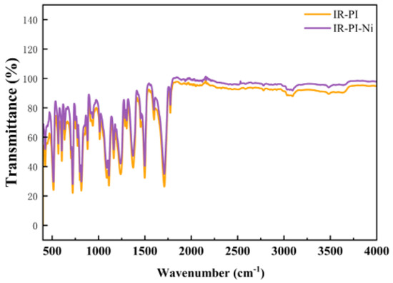
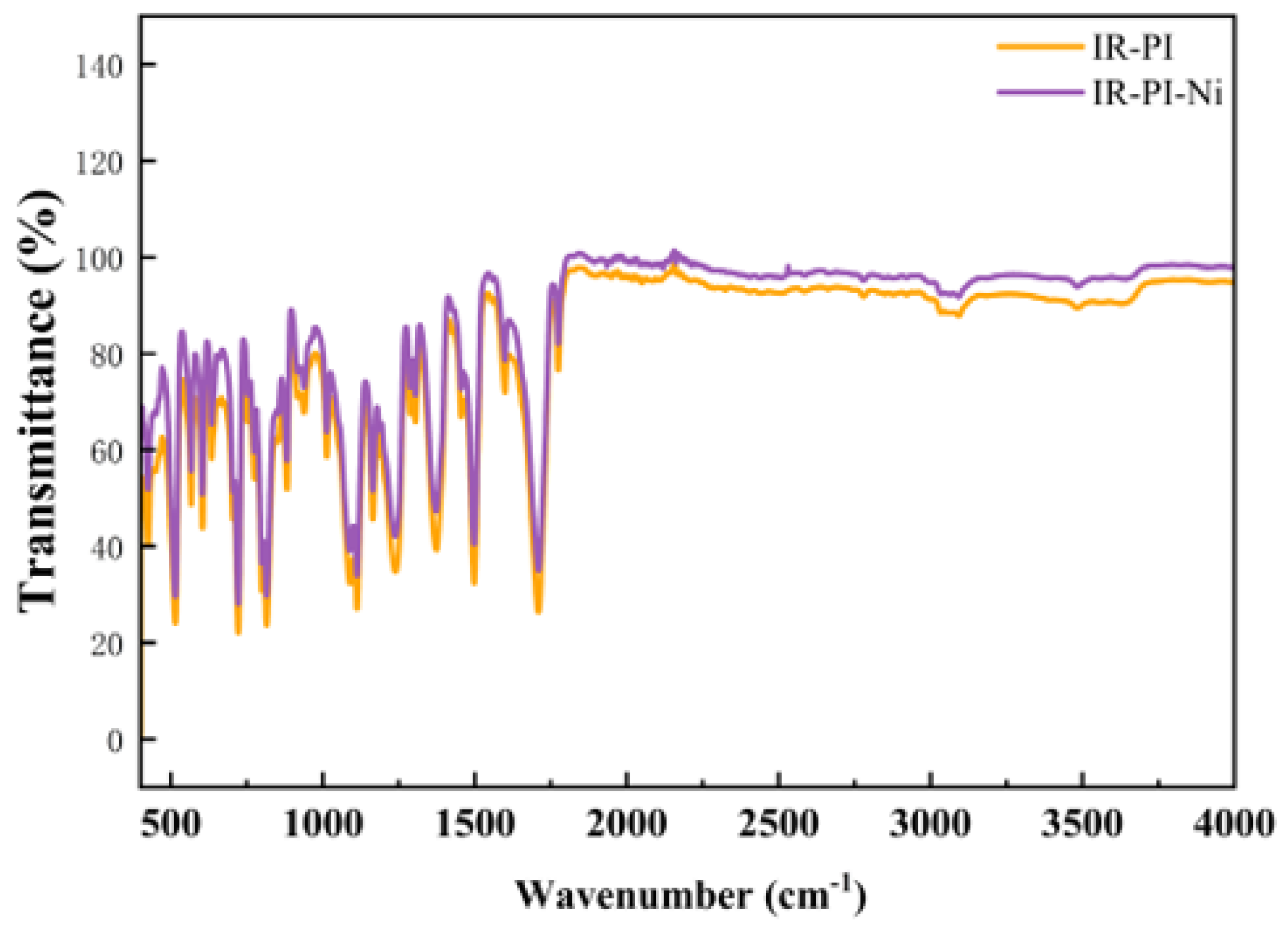
The surface chemical structures of pristine and Ni-ion-implanted PI were examined using ATR-FTIR and XPS, as shown in Figure 1 and Figure 2. The ATR-FTIR transmittance spectra in Figure 1 exhibited similar overall profiles over the range of 4000–400 cm−1, and the principal absorption bands of aromatic PI remained detectable after implantation. For pristine PI, the bands at 1774.7 and 1709.1 cm−1 were assigned to the asymmetric and symmetric stretching vibrations of the imide C=O groups, respectively, while the bands at 1373.6 and 721.2 cm−1 were associated with imide C–N stretching and imide-ring deformation. The bands at 1599.2 and 1497.5 cm−1 originated from aromatic-ring skeletal vibrations, whereas those at 1238.6, 1164.3, and 1112.7 cm−1 were mainly related to C–N and C–O–C vibrations.
Figure 1.
ATR-FTIR spectra of pristine PI (IR-PI) and PI after Ni-ion implantation at 5 keV and 1 × 10¹⁴ ions cm−2 (IR-PI-Ni).
Figure 2.
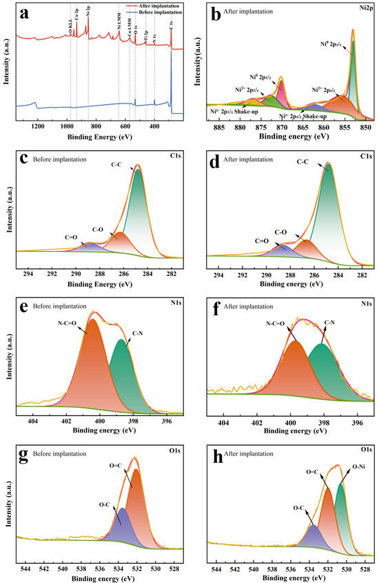
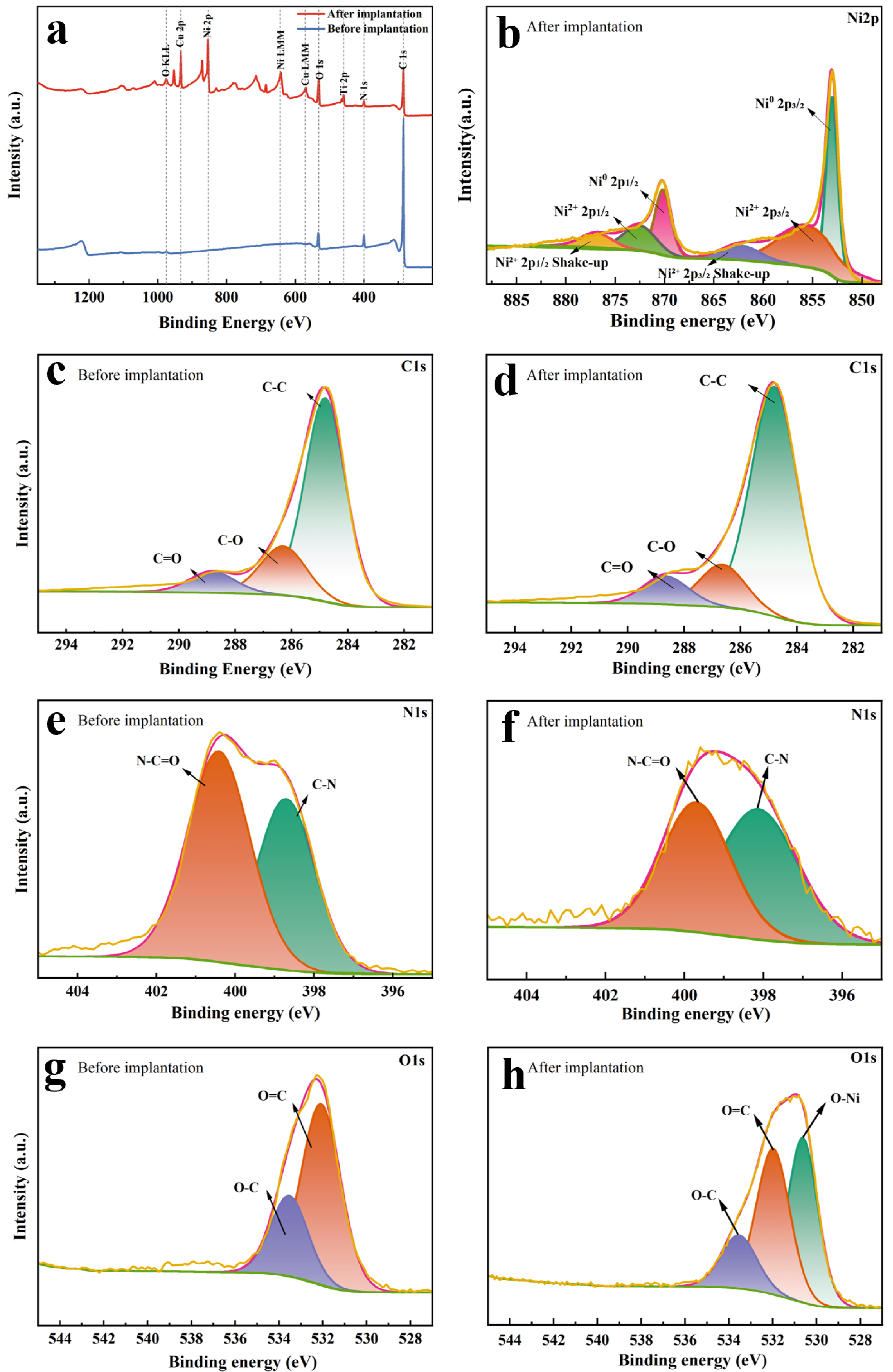
XPS spectra of pristine PI and PI after Ni-ion implantation at 5 keV and 1 × 10¹⁴ ions cm−2: (a) survey spectra; (b) high-resolution Ni 2p spectrum of implanted PI; (c,d) high-resolution C 1s spectra before and after implantation, respectively; (e,f) corresponding N 1s spectra; and (g,h) corresponding O 1s spectra.
Ni-ion implantation caused only minor shifts in the characteristic band positions, generally not exceeding 1.5 cm−1, and no distinct new absorption band or pronounced broadening was observed. However, the major absorption valleys became systematically shallower after implantation. The relative valley depths of the imide C=O bands at 1774.7 and 1709.1 cm−1 decreased from 16.0% and 56.6% to 12.2% and 42.4%, respectively. The relative valley depth of the imide C–N band near 1373.6 cm−1 decreased from 44.4% to 34.5%, while that of the imide-ring deformation band near 721.2 cm−1 decreased from 65.5% to 56.8%. The C–N- and C–O–C-related bands near 1238.6, 1164.3, and 1112.7 cm−1 also weakened after implantation. These coordinated decreases are consistent with partial disruption of imide-related bonding and chemical-bond rearrangement in the near-surface region, although the ATR-FTIR data alone do not uniquely establish chain scission. The persistence of the principal imide and aromatic bands suggests that the main PI framework remained detectable after implantation; however, these surface-sensitive measurements do not directly establish the condition of the bulk polymer.
The XPS survey spectra in Figure 2a show that pristine PI was mainly composed of C, N, and O. After Ni-ion implantation, a distinct Ni-related signal appeared, providing direct evidence that Ni was present within the XPS sampling depth. The Ti and Cu signals originate from impurity elements introduced by the baffles inside the chamber. Variations in the relative intensities of the C, N, and O signals further indicated that energetic-ion bombardment altered the surface composition and local chemical environments of PI. The survey spectra are therefore consistent with a Ni-containing modified surface region comprising residual PI structures and Ni-related chemical states; implantation-induced defects are inferred from, rather than directly identified by, these measurements.
The pristine PI spectrum is dominated by the characteristic C 1s, N 1s, and O 1s signals of the polyimide backbone. In contrast, the implanted sample exhibits an intense Ni 2p signal in the 850–875 eV region together with a pronounced Ni LMM Auger feature, providing direct spectral evidence for Ni within the XPS sampling depth. Minor extrinsic signals introduced during sample processing are excluded from the present discussion, and only the intrinsic PI elements and implanted Ni are considered below.
According to the quantitative peak in Table 1, pristine PI contains 89.34 at.% C, 5.65 at.% N, and 5.01 at.% O. After Ni-ion implantation, the measured surface composition changes to 60.18 at.% C, 5.31 at.% N, 15.65 at.% O, and 10.98 at.% Ni for the principal species considered here. The decrease in the relative C fraction should not be interpreted solely as direct carbon removal, because the measured atomic percentages are also affected by the newly incorporated Ni and by the redistribution of near-surface constituents. Nevertheless, the O/C atomic ratio increases markedly from 0.056 to 0.260, corresponding to an approximately 4.6-fold increase, while the N content changes only slightly. This increase in the measured O/C ratio is consistent with a marked change in the relative abundance of oxygen-containing species at the PI surface after Ni-ion implantation [15].
Table 1.
Principal surface composition and core-level parameters.
The peak positions further support implantation-induced modification of the near-surface chemical environment. The C 1s maximum remains at 284.80 eV for both samples, whereas the N 1s peak shifts slightly from 399.82 to 399.55 eV. More notably, the O 1s peak shifts from 532.28 eV in pristine PI to 531.05 eV after implantation, accompanied by an increase in FWHM from 2.76 to 3.07 eV. The lower average O 1s binding energy and peak broadening indicate the appearance of additional oxygen chemical environments at lower binding energy in the implanted surface. However, specific assignments to individual oxygen-containing bonds should be based on high-resolution O 1s deconvolution rather than on the survey spectrum alone.
The Ni 2p3/2 peak is located at 852.98 eV in the high-resolution peak table. Together with the strong Ni LMM Auger signal in the survey spectrum, this provides two independent spectral signatures of Ni incorporation. At the survey level, these data indicate a pronounced change in the near-surface composition after 5 keV Ni-ion implantation, characterized by detectable Ni and a substantial increase in the relative abundance of oxygen-containing species, while the nitrogen fraction remains comparatively stable. Detailed changes in carbon bonding, nitrogen functionality, oxygen coordination, and Ni chemical states are therefore examined more appropriately using the corresponding high-resolution C 1s, N 1s, O 1s, and Ni 2p spectra.
The high-resolution C 1s spectra after implantation in Figure 2d were deconvoluted into three principal components centered at approximately 284.8, 286.2, and 288.5 eV, corresponding to C–C, C–O, and imide carbonyl C=O environments, respectively. Compared with pristine PI in Figure 2c, the implanted specimen did not exhibit an additional carbon-related component or a pronounced shift in the fitted peak positions. Instead, the relative contributions of the C–O and carbonyl-related components decreased or were redistributed, whereas the C–C contribution became relatively more prominent. These changes are consistent with a redistribution of ether- and imide-related carbon environments and carbonaceous rearrangement in the near-surface region; however, the C 1s spectra alone do not distinguish uniquely among bond cleavage, deoxygenation, and crosslinking pathways. The principal spectral change is therefore interpreted as redistribution of the original carbon chemical states rather than formation of a completely new carbon-bonding environment.
The high-resolution N 1s spectra of pristine PI in Figure 2e consist mainly of C–N and N–C=O components centered at approximately 399.5 and 400.5–401.0 eV, respectively. Following Ni-ion implantation in Figure 2f, no clearly resolved independent nitrogen-related component was observed, but the relative contribution of the N–C=O component decreased. This change is consistent with partial disruption or opening of the imide rings and agrees with the decreases in the carbonyl- and C–O-related components observed in the C 1s spectra. Although possible Ni–N coordination cannot be entirely excluded because its binding-energy region may overlap with the intrinsic nitrogen environments of PI, the present N 1s spectra do not provide sufficiently resolved evidence for a definitive Ni–N assignment. Accordingly, the current XPS data are more consistent with Ni–O–related species than with a uniquely resolved Ni–N assignment [14,15].
As shown in Figure 2g and Table 2, for pristine PI, the O 1s envelope is centered at 532.28 eV with an overall FWHM of 2.76 eV and an O concentration of 5.01 at.%. Deconvolution resolves two principal oxygen environments at 531.97 eV and 533.37 eV. The lower-binding-energy component is assigned to imide carbonyl oxygen (C=O), whereas the higher-binding-energy component is attributed primarily to ether oxygen (C–O–C) in the PI backbone. Their fitted area fractions are approximately 64.8% and 35.2%, respectively. These two contributions are consistent with the expected chemically inequivalent oxygen sites in aromatic polyimide.
Table 2.
Fitted O 1s components of pristine and Ni-ion-implanted PI.
After implantation (shown in Figure 2h), the overall O 1s maximum shifts to 531.05 eV, and the envelope broadens to 3.07 eV. As shown by the fitted O 1s components of pristine and Ni-ion-implanted PI in Table 2, the measured oxygen concentration increases to 15.65 at.%. The implanted spectrum requires an additional low-binding-energy contribution at 530.42 eV, together with components at 531.68 and 533.11 eV. The 530.42 eV component is tentatively assigned to Ni–O–related oxygen or oxygen coordinated to implanted Ni species; the 531.68 eV component is associated mainly with residual or modified imide carbonyl groups; and the 533.11 eV component is attributed to C–O–C and other higher-binding-energy C–O environments. The corresponding fitted fractions are approximately 38.8%, 40.4%, and 20.9%. The appearance of the low-binding-energy O component, together with the increased oxygen content and the downshift and broadening of the O 1s envelope, is consistent with a substantial change in the local oxygen coordination environment at the PI surface after Ni implantation.
For the implanted sample, the fitted Ni 2p3/2 components are summarized in Table 3, and the corresponding high-resolution Ni 2p spectrum is shown in Figure 2b. Ni accounts for 10.98 at.% in the instrument peak table, and the dominant Ni 2p3/2 peak is located at 852.98 eV. The full high-resolution spectrum also exhibits the corresponding Ni 2p1/2 feature near 870.2 eV, consistent with the characteristic Ni 2p spin–orbit doublet. Deconvolution of the Ni 2p3/2 region gives a sharp component at 852.99 eV, a broader component at 854.83 eV, and a broad shake-up feature centered at approximately 860.10 eV. The 852.99 eV contribution is characteristic of metallic Ni-like species, whereas the 854.83 eV contribution is assigned to oxidized Ni2+/Ni–O–related species. The high-binding-energy feature is treated as the shake-up/multiplet satellite envelope associated with oxidized Ni. Considering only the two principal chemical-state components and excluding the satellite intensity, the fitted main-state contributions are approximately 66.2% metallic Ni-like and 33.8% oxidized Ni-related. Thus, implanted Ni is predominantly present in a metallic-like state, while a substantial fraction participates in Ni–O–type coordination or oxidation at the modified PI surface. This interpretation is also consistent with the new low-binding-energy O 1s component at 530.42 eV.
Table 3.
Fitted Ni 2p3/2 components of Ni-ion-implanted PI.
Taken together, the O 1s and Ni 2p results are consistent with modification of the local oxygen chemical environment in the near-surface region after Ni implantation. Pristine PI is dominated by the expected imide carbonyl and ether oxygen states. After implantation, a distinct low-binding-energy oxygen component appears and the O 1s envelope shifts and broadens, while Ni 2p contains both metallic-like and oxidized Ni–related contributions. Corresponding features in the two core levels support the assignment of Ni–O–related species, although XPS alone does not establish a unique interfacial bonding configuration. The persistence of the carbonyl and C–O components suggests that residual PI oxygen functionalities remain. Accordingly, the XPS data are most consistent with a mixed surface state comprising implanted metallic-like Ni, Ni–O–related species, and modified PI oxygen environments. Such changes may increase surface chemical activity and provide additional sites for subsequent metal nucleation and interfacial bonding.
Overall, the ATR-FTIR and XPS results are consistent with modification of the surface and near-surface chemical environment of PI by Ni-ion implantation. The spectral changes suggest partial disruption or rearrangement of imide-, ether-, and nitrogen-containing structures and are compatible with the presence of Ni–O–related species, while the principal aromatic PI bands remain detectable. These observations may help explain the measured increase in surface polarity and could favor adsorption and nucleation of the subsequently deposited metallic interlayer; they do not, however, by themselves prove a specific bonding or adhesion mechanism.
The changes in surface wettability and surface free energy are summarized in Table 4. After Ni-ion implantation, the water contact angle decreased from 75° to 64°, while the diiodomethane contact angle decreased from 52° to 47°. Correspondingly, the total surface free energy increased from 36.41 to 42.99 mJ m−2, representing an increase of approximately 18%.
Table 4.
Contact angles and surface-free-energy components of pristine and Ni-ion-implanted PI.
The dispersive component remained nearly unchanged, increasing slightly from 27.47 to 27.99 mJ m−2. In contrast, the polar component increased from 8.94 to 14.99 mJ m−2, corresponding to an increase of approximately 68%. Therefore, the increase in total surface free energy was primarily attributed to the enhanced polar contribution rather than to a change in dispersive interactions.
The pronounced increase in the polar component is consistent with the generation of chemically active or polar sites through ion-induced bond scission and reconstruction [8,11,14,15], although contact-angle measurements do not identify specific surface species. Higher surface free energy is generally favorable for wetting and adsorption of incoming metal species and may increase the nucleation density of the subsequently deposited Ni layer. The present contact-angle results therefore establish improved wettability and polarity, but they do not by themselves determine the subsequent nucleation or bonding mechanism.
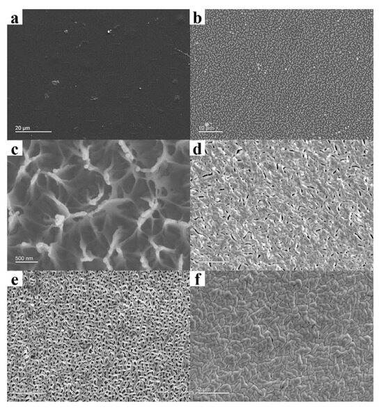
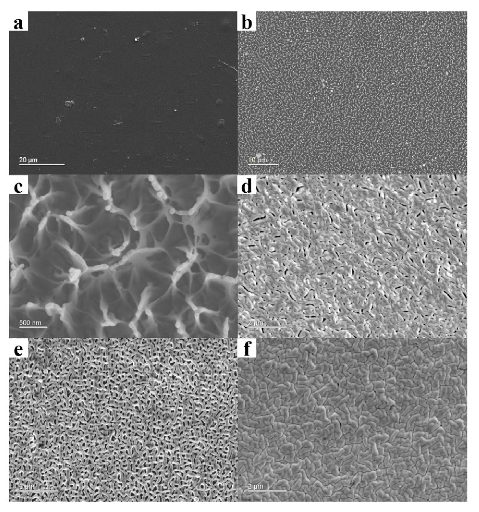
The surface morphologies of pristine and implanted PI are compared in Figure 3a–c. The pristine PI exhibited a relatively smooth and featureless surface at both low and high magnifications, whereas the implanted PI showed uniformly distributed micro/nanoscale surface features. At higher magnification, pore-like structures with characteristic dimensions of approximately 50–300 nm, together with localized fibrous protrusions, were clearly observed. AFM analysis further quantified this implantation-induced surface evolution: the root-mean-square roughness, Sq increased from approximately 2–3 nm for pristine PI to 4–7 nm after implantation, representing at least a twofold increase. This increase in nanoscale roughness is consistent with the SEM observations and indicates that ion implantation effectively modified the near-surface morphology without causing severe macroscopic damage.
Figure 3.
Surface morphologies of the PI substrates and deposited Cu films: (a) pristine PI; (b,c) PI after Ni-ion implantation at 5 keV and 1 × 10¹⁴ ions cm−2 at low and high magnification, respectively; (d) 2 μm Cu on S1 (untreated PI/20 nm Ni); (e) 2 μm Cu on S2 (untreated PI/10 nm Ni); and (f) 2 μm Cu on S3 (Ni-ion-implanted PI/5 nm Ni). Scale bars: 20 μm (a), 10 μm (b), 500 nm (c), and 2 μm (d–f).
The formation of these micro/nanoscale features and the accompanying increase in surface roughness are expected to enlarge the effective interfacial area and provide additional geometrical sites for metal adsorption, nucleation, and mechanical anchoring. Importantly, no obvious large cracks, delamination, or severe surface deterioration were observed after implantation, suggesting that the surface modification remained predominantly confined to the micro/nanoscale. Combined with the implantation-associated increase in surface polarity, the modified morphology may provide chemical and physical conditions favorable for nucleation, growth, and interfacial stabilization of the ultrathin Ni interlayer.
The surface morphologies of the deposited Cu films are shown in Figure 3d–f. The Cu film on S1, which contained a 20 nm Ni interlayer, exhibited a relatively compact granular morphology. When the Ni thickness was reduced to 10 nm without implantation, the Cu film on S2 showed a less uniform surface with more pronounced void-like defects. This result suggests that the thinner Ni layer deposited directly on untreated PI did not provide sufficiently uniform coverage during the initial growth stage. Defects generated in the discontinuous or weakly connected Ni layer were subsequently inherited and enlarged during Cu deposition.
In contrast, the Cu film on S3 exhibited the most compact and uniform morphology, even though the deposited Ni interlayer was only 5 nm thick. Because S3 contained the thinnest deposited Ni layer, the improved Cu morphology cannot be attributed simply to an increase in Ni thickness. Instead, the higher surface polarity and implantation-induced micro/nanostructures likely increased the adsorption and nucleation density of Ni atoms, enabling the 5 nm layer to form more uniformly. This compact ultrathin Ni layer then acted as a favorable template for the subsequent growth of Cu. Similar relationships between polymer activation, enhanced metal nucleation, suppression of isolated island growth, and improved coating compactness have been reported for plasma- and ion-beam-treated PI surfaces [7,8,10,11].
2.2. Formation of the Ultrathin Graded Interface
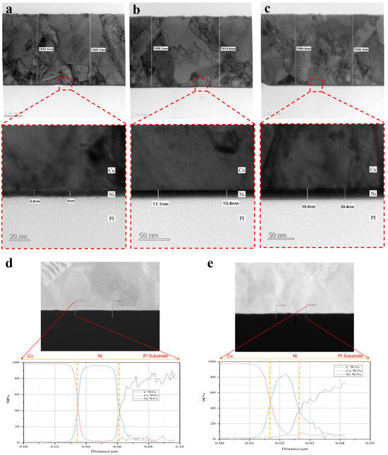
The cross-sectional structures of the three Cu/Ni/PI configurations are shown in Figure 4a–c, corresponding to S3, S2, and S1, respectively. In S1 (Figure 4c), the deposited Ni layer had a thickness of approximately 20 nm and formed a distinguishable transition layer between the PI substrate and the Cu coating. The Ni/PI interface was comparatively flat, indicating that the Ni layer was mainly deposited on the outer surface of untreated PI.
Figure 4.
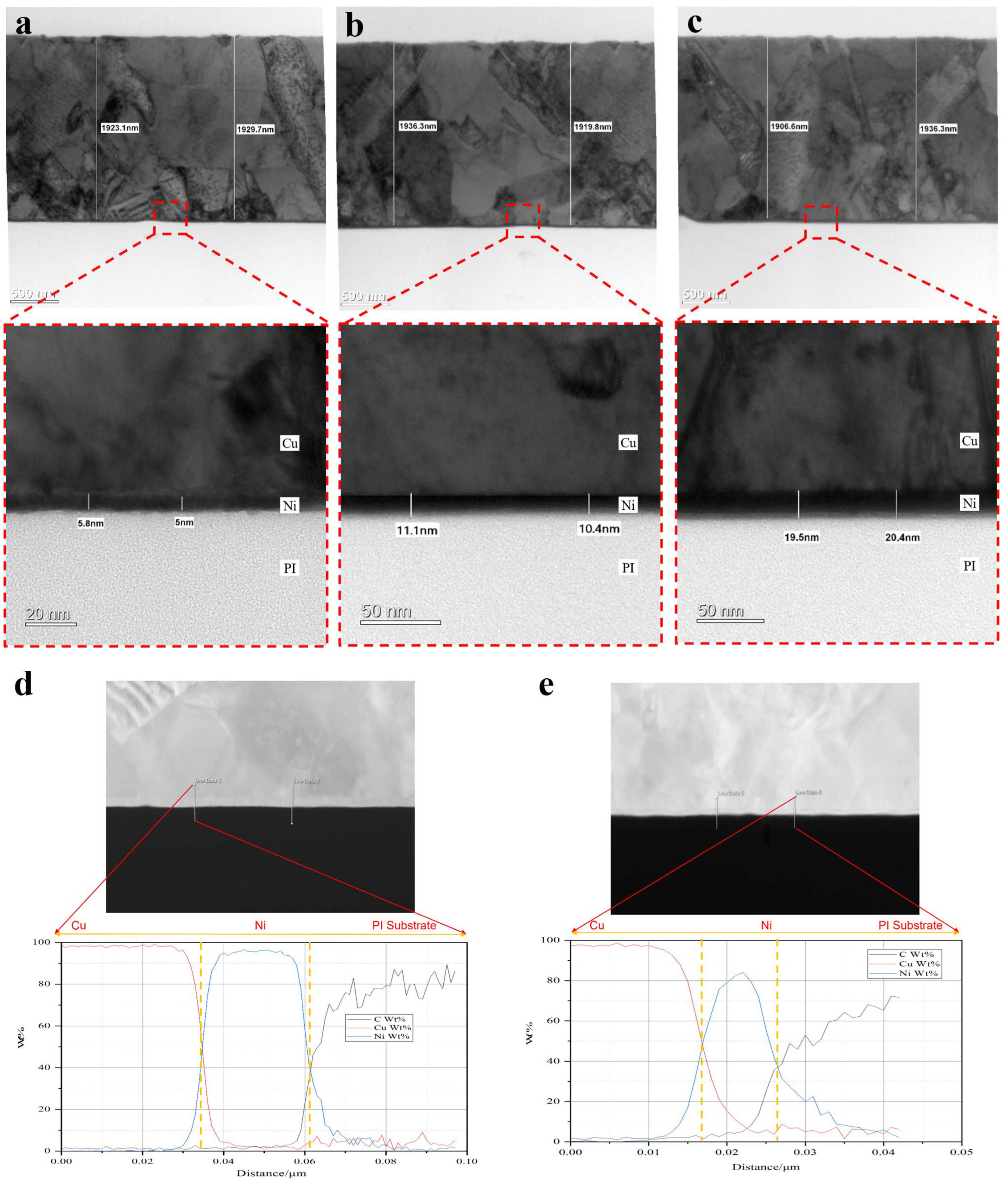
Cross-sectional microstructures and elemental distributions of the Cu/Ni/PI interfaces: (a) S3 (Ni-ion-implanted PI/5 nm Ni/2 μm Cu); (b) S2 (untreated PI/10 nm Ni/2 μm Cu); (c) S1 (untreated PI/20 nm Ni/2 μm Cu); (d) EDX line-scan profile across the S1 interface; and (e) EDX line-scan profile across the S3 interface. Scale bars: 500 nm in the upper images of (a–c), 20 nm in the magnified image of (a), and 50 nm in the magnified images of (b,c).
A similar flat interface was observed for S2 (Figure 4b), although the deposited Ni thickness was reduced to approximately 10 nm. The reduction in Ni thickness did not produce an obvious embedded or graded morphology at the untreated PI surface. Therefore, in S1 and S2, the interfacial connection was primarily provided by the deposited Ni films rather than by modification of the PI subsurface.
A substantially different structure was observed in S3 (Figure 4a). Although the deposited Ni layer was only approximately 5 nm thick, the Ni/PI boundary exhibited an undulating and locally embedded morphology. The shape of this boundary corresponded to the micro/nanoscale surface features observed after Ni-ion implantation in Figure 3b,c. The deposited Ni layer conformed to the irregular PI surface and locally entered the implantation-induced depressions rather than simply covering a flat substrate.
The undulating, locally embedded morphology would be expected to increase the real Ni/PI contact area and is consistent with a possible mechanical-anchoring contribution. If mechanical interlocking contributes, local sliding and crack propagation may follow a more tortuous separation path than at the comparatively flat S1 and S2 interfaces. Similar contributions from ion- or plasma-induced surface structures have been proposed for other metal/polymer interfaces [10,27,30].
The EDX line-scan profiles further revealed distinct elemental-transition characteristics for S1 and S3. In S1, the C-, Ni-, and Cu-related signals changed relatively abruptly across the PI/Ni and Ni/Cu interfaces, as shown in Figure 4d. This behavior is consistent with the comparatively flat and discrete multilayer structure observed by TEM.
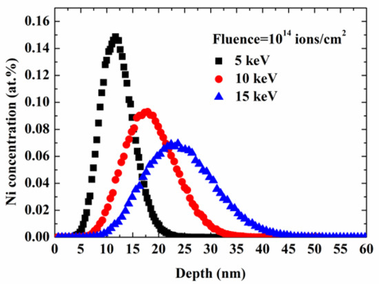
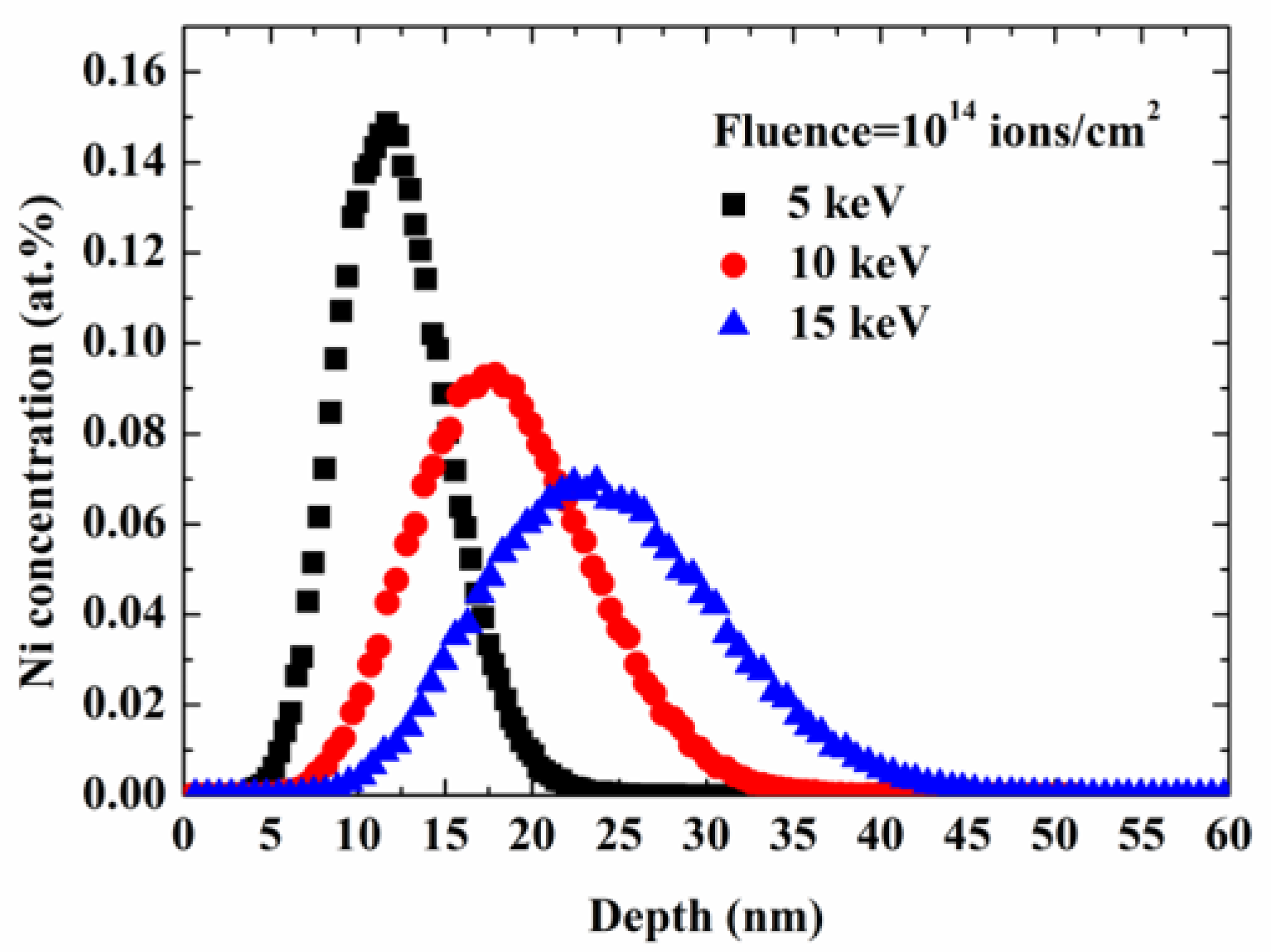
In contrast, the elemental signals in S3 exhibited a more gradual variation across the modified interfacial region, consistent with an apparent compositional transition rather than an abrupt interface. Local EDX point analyses further detected approximately 0.54 and 0.37 at.% Ni at positions about 10 and 20 nm below the nominal PI/Ni boundary, respectively. The depth range over which Ni was detected is comparable to the near-surface Ni distribution predicted by the 5 keV SRIM simulation in Figure 5, in which the maximum Ni concentration was located at a depth of approximately 11 nm.
Figure 5.
SRIM-simulated Ni concentration profiles in PI at 5, 10, and 15 keV for a fluence of 1 × 10¹⁴ ions cm−2.
The nominal spatial resolution of the EDX analysis was approximately 1–2 nm. Although the finite probe size can broaden the measured elemental-transition profile, the observed Ni-containing region extending to approximately 20 nm below the nominal interface is substantially wider than this resolution, making it unlikely that the entire gradient arose from spatial resolution alone. The apparent transition width may also be affected by electron-beam broadening, specimen thickness, and local interface inclination; therefore, the EDX profile should not be treated as a direct measurement of the exact atomic interdiffusion distance. Taken together, the gradual signal overlap, subsurface detection of Ni by EDX, cross-sectional TEM morphology, and SRIM-predicted implantation profile are consistent with—but do not definitively prove—an apparent Ni-containing graded region linking the modified PI subsurface and the subsequently deposited 5 nm Ni layer.
On the basis of these observations, the S3 interface is interpreted as an ultrathin composite transition region rather than a simple abrupt PI/Ni/Cu stack. The proposed region includes Ni-modified PI, a locally embedded 5 nm deposited Ni layer, and the overlying Cu coating. The data are consistent with implantation extending the interfacial modification into the near-surface PI and thereby reducing the apparent structural and compositional discontinuity between the polymer and the metal [27,28,29,30,31].
The observed S3 interface is consistent with combined effects of ion implantation and subsequent physical vapor deposition. First, implanted Ni and ion-induced structural changes may modify the near-surface PI. Second, the measured increase in surface polarity and the observed micro/nanoscale features may favor nucleation and retention of deposited Ni atoms. Third, the 5 nm Ni layer conforms to the modified surface, producing an apparent connection between the Ni-containing subsurface region and the Cu coating. The XPS data are consistent with Ni–O-related species, whereas Ni–N coordination is not resolved; therefore, any specific chemical-bonding contribution remains provisional [14,15].
2.3. Adhesion and Electrical Performance
All three as-deposited 2 μm Cu-coated specimens achieved a 5B rating in the cross-cut tape test, indicating that no extensive coating removal occurred under the qualitative test conditions. For quantitative evaluation, the Cu layers were electroplated from 2 μm to a total thickness of approximately 18 μm to produce mechanically stable peel strips, consistent with the specimen-thickness requirement for flexible metal-clad peel testing in IPC-TM-650 2.4.9 [32]. The 180° peel-test configuration is schematically shown in Figure 6, where the Cu layer was peeled back at 180° relative to the substrate surface and the peel force was recorded continuously. Because all specimens were electroplated under identical bath, current-density, and deposition-time conditions, the measured peel strengths provide a controlled comparison of the relative peel performance of the three complete metallization configurations. However, these values should not be interpreted as the intrinsic interfacial adhesion of the as-deposited 2 μm Cu films. Electroplating may modify the Cu microstructure and residual-stress state and thereby influence the subsequent failure path. In the absence of post-peel fracture-surface and residual-stress analyses, the contribution of electroplating cannot be separated from that of the original interface and therefore remains a limitation of the present peel-strength comparison.
Figure 6.
Schematic of the 180° peel-test configuration.
The present study focuses on the initial interfacial structure and adhesion behavior. Long-term reliability under repeated bending, thermal aging, and humidity exposure was not evaluated. Although the simulated implantation depth is only in the order of tens of nanometers compared with the 25 μm PI thickness, dedicated mechanical and dielectric measurements are required to determine whether ion implantation affects the bulk mechanical integrity or dielectric properties of the substrate. These issues will be addressed in future work.
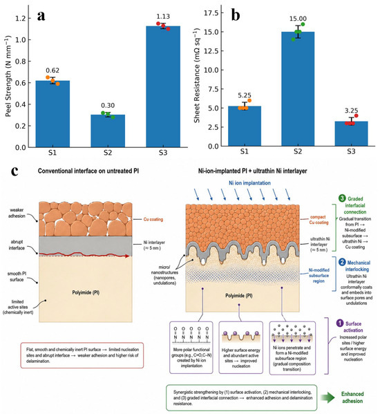
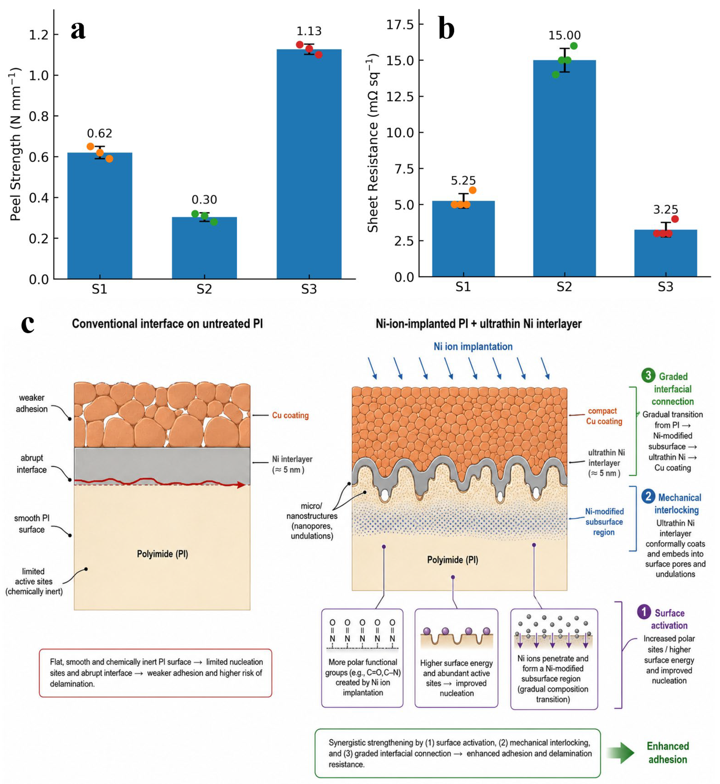
As shown in Figure 7a, the average peel strengths of S1, S2, and S3 were 0.62, 0.30, and 1.13 N mm−1, respectively. Reducing the deposited Ni thickness from 20 nm in S1 to 10 nm in S2 decreased the peel strength by approximately 52%. Under the present processing conditions, this result shows that simply reducing the deposited Ni thickness from 20 to 10 nm did not maintain the measured peel strength. The deterioration is consistent with the less compact Cu-film morphology observed for S2, which suggests incomplete or nonuniform coverage of the untreated PI by the thinner Ni layer.
Figure 7.
Adhesion and electrical properties of the Cu/Ni/PI specimens: (a) average 180° peel strength (n = 3) and (b) sheet resistance (n = 4) of S1, S2, and S3. Bars show mean values, error bars show standard deviations, and symbols show individual measurements. (c) Evidence-consistent schematic of possible interfacial contributions associated with Ni ion implantation and the ultrathin Ni interlayer. S1 = untreated PI/20 nm Ni/2 μm Cu; S2 = untreated PI/10 nm Ni/2 μm Cu; S3 = Ni-ion-implanted PI/5 nm Ni/2 μm Cu. Panel (c) is a conceptual, not-to-scale interpretation and does not represent an additional untreated-PI/5 nm Ni control specimen.
In contrast, S3 exhibited the highest peel strength despite having the thinnest deposited Ni interlayer. Compared with S1, the deposited Ni thickness was reduced from 20 to 5 nm, corresponding to a reduction of 75%, while the peel strength increased by approximately 82%. Compared with S2, the peel strength of S3 increased by approximately 277%.
These results indicate that nominal Ni thickness alone does not explain the observed adhesion trend. The differences are consistent with contributions from interlayer continuity, the chemical and morphological state of the PI surface, and the structure of the transition region. Interlayer thickness and continuity have similarly been identified as critical parameters for Cu/PI adhesion [9,10,14,15]. Representative metal/PI adhesion results reported for different surface-modification strategies are summarized in Table 5. O2 ion-beam and Ar/N2 plasma treatments improve metal adhesion mainly by introducing active surface functionalities and/or increasing surface roughness [11,33], whereas Ni-plasma and Ni+-implantation treatments additionally generate an implanted or compositionally modified interfacial region that can facilitate chemical coordination, cross-linking, and mechanical interlocking with subsequently deposited metal layers [14,15]. The reported peel-adhesion values range from approximately 0.20 N/mm for untreated NiCr/PI in Ref. [11] to 1.0 N/mm for plasma-treated Cu/PI [33] and 1.93 ± 0.21 N/mm for the Ni+-implantation/CuNi-buffer architecture [14]. Although direct numerical comparison is influenced by differences in surface-treatment conditions, metal-layer configurations, and peel-test geometries, the literature generally indicates that energetic-ion and plasma activation can substantially enhance metal/PI interfacial adhesion. Together with the present results, these comparisons suggest that high adhesion is associated with the combined control of interlayer thickness and continuity, PI surface chemistry and morphology, and the structure of the interfacial transition region.
Table 5.
Comparison of representative PI surface-treatment methods and metal/PI peel adhesion reported in the literature.
The higher peel strength observed for S3 may be interpreted in terms of three mutually reinforcing contributions, as illustrated by the proposed conceptual model in Figure 7c. First, the measured increase in surface free energy, particularly its polar component, may favor the wetting, adsorption, and nucleation of the deposited Ni. Second, the implantation-induced micro/nanoscale features and the locally embedded Ni/PI morphology may increase the effective contact area and provide a possible mechanical-anchoring contribution. Third, the TEM and EDX observations are consistent with the presence of a Ni-containing gradual transition region connecting the modified PI subsurface with the deposited Ni layer. These observations collectively support the proposed adhesion-enhancement mechanism; however, they do not independently establish the contribution of each mechanism or prove a direct causal relationship with the measured peel strength.
The sheet-resistance results are presented in Figure 7b. The average sheet resistances of S1, S2, and S3 were 5.25, 15.00, and 3.25 mΩ sq−1, respectively. S2 exhibited the highest sheet resistance, which was consistent with its relatively defective Cu morphology. Voids, discontinuities, and weakly connected grains reduce the effective current-carrying cross-section of the coating and introduce local constrictions into the conductive path.
S3 exhibited the lowest measured sheet resistance, corresponding to reductions of approximately 38% and 78% relative to S1 and S2, respectively. Because the Cu layer was much thicker than the Ni interlayer, the differences in sheet resistance should not be interpreted mainly as the intrinsic resistance contribution of 5, 10, or 20 nm Ni. Instead, the measured resistance differences are consistent with treatment-related changes in Cu nucleation, continuity, and compactness. The more compact morphology of S3 may have provided more continuous conductive pathways and fewer defect-related constrictions. Surface activation and interlayer design have likewise been reported to influence both the morphology and electrical properties of metal films deposited on polymer substrates [7,8,25].
Before testing, the 2 μm PVD Cu layer was electroplated to a total Cu thickness of approximately 18 μm; the arrow indicates the peel direction. The schematic is not to scale.
Overall, the results are consistent with the interpretation that Ni-ion implantation can transfer part of the adhesion-promoting role from the deposited Ni film to the modified PI subsurface. Under the specific conditions examined, S3 combined a 5 nm deposited Ni layer with higher peel strength and lower sheet resistance than S1 and S2, which contained thicker Ni layers on untreated PI. The proposed interfacial design may therefore permit a reduction in deposited Ni thickness while retaining favorable adhesion and electrical continuity; however, the individual mechanistic contributions require separate validation.
Although device-level power consumption was not directly evaluated, a mechanically reliable metallization structure with low sheet resistance is favorable for reducing interconnect voltage drop and ohmic conduction loss. The present results therefore provide a materials and interface-engineering basis for further development of thin and reliable Cu/PI interconnects.
3. Materials and Methods
3.1. Sample Preparation
Commercial PI films(DuPont, Wilmington, DE, USA) with a thickness of 25 μm were cut into specimens measuring 10 cm × 10 cm. Before metallization, the PI specimens were ultrasonically cleaned in ethanol(Chengdu Lianhe Chemical & Pharmaceutical Co., Ltd, Chengdu, China) for 15 min, dried with nitrogen(Sichuan Tianyuan Gas Co., Ltd., Deyang, China), and fixed on the substrate holder in the vacuum chamber.
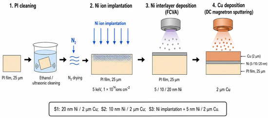
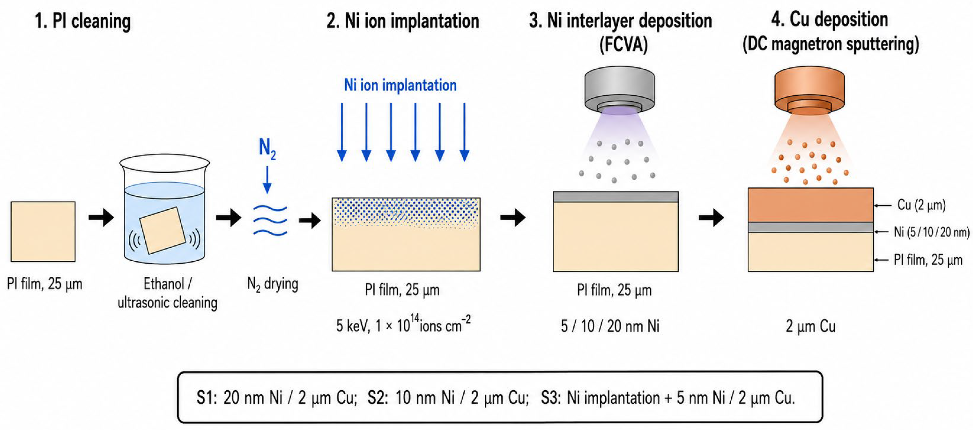
Three Cu/Ni/PI metallization configurations were prepared. For sample S1, a 20 nm Ni interlayer was deposited on untreated PI, followed by a 2 μm Cu layer. Sample S2 was prepared using the same procedure, except that the Ni interlayer thickness was reduced to 10 nm. For sample S3, the PI surface was first implanted with Ni ions at an energy of 5 keV and a fluence of 1 × 10¹⁴ ions cm−2. A 5 nm Ni interlayer and a 2 μm Cu layer were subsequently deposited. The schematic illustration of the preparation workflows for all three samples is presented in Figure 8.
Figure 8.
Schematic illustration of sample preparation and Ni ion implantation: fabrication sequence and definitions of S1 (untreated PI/20 nm Ni/2 μm Cu), S2 (untreated PI/10 nm Ni/2 μm Cu), and S3 (Ni-ion-implanted PI/5 nm Ni/2 μm Cu).
Prior to metallization, Ni ions were implanted into the polyimide (PI) substrates using a metal vapor vacuum arc (MEVVA) ion source(Tongchuang (Chengdu) Technology Co., Ltd., Chengdu, China ). Subsequently, Ni interlayers were deposited by filtered cathodic vacuum arc (FCVA)(Tongchuang (Chengdu) Technology Co., Ltd., Chengdu, China) deposition at an arc current of 60 A. The deposition times were 4, 2, and 1 min for samples S1, S2, and S3, respectively. During Ni deposition, Ar (Sichuan Tianyuan Gas Co., Ltd., Deyang, China) was used as the working gas, the working pressure was maintained at 0.08 Pa, and the chamber temperature was controlled at 100 ± 5 °C. After formation of the Ni interlayers, Cu layers were deposited by direct-current (DC) magnetron (Tongchuang (Chengdu) Technology Co., Ltd., Chengdu, China) sputtering at a sputtering power of 1 kW for 20 min. For Cu deposition, Ar was used as the working gas, with a working pressure of 0.2 Pa and a chamber temperature of 100 ± 5 °C. These processing conditions were kept constant for all samples unless otherwise specified. The detailed processing parameters are summarized in Table 6.
Table 6.
Processing parameters used for the preparation of the Cu/Ni/PI specimens.
The implantation depth of Ni ions in polyimide (PI) was estimated using the Stopping and Range of Ions in Matter (SRIM-2013, Ziegler, Annapolis, MD, USA) program [30] at implantation energies of 5, 10, and 15 keV, with a constant fluence of 1 × 10¹⁴ ions cm−2. The aim was to identify a shallow implantation condition that could promote interfacial interaction with the subsequently deposited metal layer while minimizing modification of the PI substrate. Previous studies have shown that pronounced irradiation-induced changes in PI, including increases in hardness and elastic modulus, chain scission, cross-linking, carbonization, changes in dielectric loss and conductivity, and reduction of dielectric strength, generally become more significant at higher ion fluences and/or irradiation energies [12,13,17,18,19,20,21,22,23,24]. Low-energy Ni implantation has also been reported to mainly affect the near-surface region of PI [14,15]. Therefore, at the relatively low fluence used here, the influence of Ni implantation on the overall mechanical integrity and bulk dielectric properties of the PI film is expected to be limited.
It should be noted that the mechanical and dielectric properties of the implanted PI specimens were not directly measured in the present study. Accordingly, this assessment is an inference based on the implantation conditions and trends reported in the literature rather than a direct experimental conclusion. Direct mechanical and dielectric measurements would be required for quantitative verification.
Among the simulated conditions, 5 keV produced the shallowest Ni distribution. As shown in Figure 5, the maximum Ni concentration was located approximately 11 nm below the PI surface, whereas higher implantation energies shifted the concentration profile deeper into the polymer. The 5 keV condition was therefore selected because it positioned the implanted Ni closest to the surface and to the subsequently deposited metallic interlayer, thereby increasing the likelihood of interfacial interaction and formation of a Ni-containing graded transition region while avoiding unnecessarily deep modification of the PI substrate.
For the quantitative peel tests, the sputtered Cu layers were further thickened to approximately 18 μm in a copper sulfate electroplating bath. Electroplating was performed at a current density of 1.5–2.0 A dm−2 for 72 min. This step provided sufficient mechanical strength for preparing the Cu strips used in the 180° peel test. Therefore, the peel test was intended to compare the complete PVD-seeded/electroplated structures rather than directly measure the intrinsic adhesion of the isolated 2 μm Cu film.
3.2. Surface and Interface Characterization
The chemical structures of pristine and Ni-ion-implanted PI surfaces were characterized by X-ray photoelectron spectroscopy using a Thermo Scientific K-Alpha system (Thermo Fisher Scientific, East Grinstead, West Sussex, UK). Survey spectra and high-resolution C 1s, O 1s, N 1s, and Ni 2p spectra were collected. The binding-energy scale was calibrated using the C–C/C=C component of the C 1s spectrum at 284.8 eV.
The molecular structures of pristine and implanted PI were further examined by attenuated-total-reflectance Fourier-transform infrared spectroscopy using a Nicolet iS50 spectrometer (Thermo Fisher Scientific, Madison, WI, USA). Spectra were recorded over the range of 4000–400 cm−1 at a resolution of 4 cm−1. XPS and ATR-FTIR measurements were conducted before deposition of the Ni and Cu layers to identify the chemical changes caused by Ni ion implantation.
The wettability of the PI surfaces was evaluated using a Theta Lite 100 (Biolin Scientific, Gothenburg, Sweden)optical contact-angle instrument. Distilled water and diiodomethane were used as probe liquids. The dispersive and polar components of the PI surface free energy were calculated using the Owens–Wendt two-liquid method [31].
The surface morphologies of pristine PI, Ni-ion-implanted PI, and the deposited Cu films were examined using a JSM-7500F field-emission scanning electron microscope (Thermo Fisher Scientific, Brno, Czech Republic). Cross-sectional lamellae were prepared by focused-ion-beam milling Helios 600i(FEI Company, Hillsboro, OR, USA) and examined by transmission electron microscopy (Tecnai F20, Thermo Fisher Scientific, Brno, Czech Republic); scanning transmission electron microscopy was used to determine the Ni- and Cu-layer thicknesses.
Elemental composition and spatial distribution across the Cu/Ni/PI interfaces were examined using an energy-dispersive X-ray spectroscopy (EDX) detector (Thermo Fisher Scientific, Brno, Czech Republic) mounted on the TEM. Line scans were acquired perpendicular to the interfaces of S1 and S3 to compare their elemental-transition profiles, and local point analyses were performed for S3. Under the present measurement conditions, the nominal spatial resolution of the EDX analysis was approximately 1–2 nm.
Atomic force microscopy (AFM, Jupiter XR, Oxford Instruments Asylum Research, Santa Barbara, CA, USA) was employed to characterize the surface morphology and roughness of the PI samples before and after Ni-ion implantation. The AFM measurements were carried out in a tapping mode over a scan area of 10 μm × 10 μm.
3.3. Adhesion and Electrical Measurements
The adhesion of the as-deposited 2 μm Cu films was first evaluated qualitatively using a cross-cut tape test with 3M Scotch 600 tap(3M Company, St. Paul, MN, USA)e according to ASTM D3359-02 [34]. Three regions were examined for each sample, and the adhesion was classified using the 0B–5B rating scale.
Quantitative adhesion measurements were performed using a 180° peel test. Before testing, the Cu layers were electroplated to a total thickness of approximately 18 μm to form mechanically stable peel strips. The tests were conducted using an XLW-PC electronic universal testing machine(Labthink Instruments Co., Ltd., Jinan, China) with reference to IPC-TM-650 [33]. The electroplating step was introduced only to provide sufficient mechanical rigidity for preparation of the peel strips. Therefore, the reported 180° peel strengths correspond to the electroplated test configuration rather than to the intrinsic peel strength of the as-deposited 2 μm Cu coating. The specimen width and peel rate were 3 mm and 100 mm min−1, respectively. Three measurements were performed for each metallization configuration, and the peel strength was expressed in N mm−1.
The sheet resistance of the Cu-coated specimens was measured using an RTS-5 four-point-probe tester(Guangzhou Four Probe Technology Co., Ltd., Guangzhou, China). Four positions were measured on each specimen, and the average sheet resistance was calculated. The measurements were conducted on the as-deposited 2 μm Cu films. The results were reported as the mean and standard deviation.
4. Conclusions
Ni ion implantation combined with an ultrathin deposited Ni interlayer provides an effective strategy for improving Cu/PI metallization. The implantation treatment increased the PI surface free energy from 36.41 to 42.99 mJ m−2, mainly through enhancement of the polar component, and generated uniformly distributed micro/nanoscale features that may favor metal nucleation and mechanical anchoring. Compared with the untreated PI specimens containing 20 and 10 nm Ni interlayers, the implanted specimen with a 5 nm deposited Ni layer showed a more compact Cu coating and an undulating, locally embedded interface; the EDX profile was consistent with an apparent gradual elemental transition. This configuration achieved the highest average peel strength of 1.13 N mm−1, representing an increase of approximately 82% relative to the 20 nm Ni specimen, while reducing the deposited Ni thickness by 75%. It also exhibited the lowest measured sheet resistance of 3.25 mΩ sq−1. Taken together, these findings are consistent with the interpretation that subsurface Ni-ion modification may assume part of the adhesion-promoting role otherwise provided by a thicker deposited interlayer, thereby allowing reduced Ni-layer thickness while retaining favorable interfacial adhesion and electrical continuity under the conditions tested. The proposed approach therefore offers a promising route for fabricating thin, low-resistance Cu/PI metallization structures with improved initial interfacial adhesion for flexible electronic interconnects.
Author Contributions
Conceptualization, M.C.; methodology, M.C.; validation, M.C., Y.Z., X.L., L.Z. and K.Y.; formal analysis, M.C., Y.Z., X.G. and J.O.; investigation, M.C. and J.Z.; writing—original draft preparation, M.C.; writing—review and editing, J.Z.; project administration, D.T.; funding acquisition, F.J. All authors have read and agreed to the published version of the manuscript.
Funding
This research was funded by the SWIP Innovation Action Program, grant number 202301XWCX003.
Data Availability Statement
The data presented in this study are available on request from the corresponding author.
Conflicts of Interest
The authors declare no conflicts of interest.
References
- Noh, B.-I.; Yoon, J.-W.; Jung, S.-B. Effect of Ni-Cr seed layer thickness on the adhesion characteristics of flexible copper clad laminates fabricated using a roll-to-roll process. Met. Mater. Int. 2010, 16, 779–784. [Google Scholar] [CrossRef] [Scilit]
- Tsai, Y.-N.; Tseng, I.-H.; Tsai, M.-H.; Chen, T.-L.; Lin, H.-P. Siloxane-assisted and chemically treated polyimide films for enhanced copper adhesion. Mater. Today Commun. 2025, 49, 114050. [Google Scholar] [CrossRef] [Scilit]
- Kubo, Y.; Tanaka, H.; Saito, Y.; Mizoguchi, A. Fabrication of a bilayer structure of Cu and polyimide to realize circuit microminiaturization and high interfacial adhesion in flexible electronic devices. ACS Appl. Mater. Interfaces 2018, 10, 44589–44602. [Google Scholar] [CrossRef] [Scilit] [PubMed]
- Tan, W.-Y.; Jian, L.-F.; Chen, W.-P.; Zhang, Y.-W.; Lu, X.-C.; Huang, W.-J.; Zhang, J.-S.; Wu, J.-W.; Feng, J.-L.; Liu, Y.-D.; et al. A facile strategy for intrinsic low-Dk and low-Df polyimides enabled by spirobifluorene groups. Chin. J. Polym. Sci. 2023, 41, 288–296. [Google Scholar] [CrossRef] [Scilit]
- Li, H.; Wang, X.; Wu, T.; Gong, Y.; Zhao, H.; Liu, Z.; Dastan, D.; Ma, K.; Hu, Z. Mechanical enhancement and dielectric properties of SiO2-contained polyimides under high frequency. J. Mater. Sci. Mater. Electron. 2023, 34, 2310. [Google Scholar] [CrossRef] [Scilit]
- Noh, B.-I.; Yoon, J.-W.; Lee, B.-Y.; Jung, S.-B. Effects of different kinds of seed layers and heat treatment on adhesion characteristics of Cu/(Cr or Ni–Cr)/PI interfaces in flexible printed circuits. J. Mater. Sci. Mater. Electron. 2011, 22, 790–796. [Google Scholar] [CrossRef] [Scilit]
- Wu, P.-Y.; Lin, C.-H.; Chen, C.-M. Study of surface metallization of polyimide film and interfacial characterization. Metals 2017, 7, 189. [Google Scholar] [CrossRef] [Scilit]
- Wang, E.; Song, Y.; Shang, L.; Zhang, G.; Wang, S. Plasma surface pretreatment to improve interfacial adhesion strengths of sputtered Cu on polyimide film. Surf. Topogr. Metrol. Prop. 2022, 10, 045005. [Google Scholar] [CrossRef] [Scilit]
- Xiang, J.; Zhou, G.; Hong, Y.; He, W.; Wang, S.; Chen, Y.; Wang, C.; Tang, Y.; Sun, Y.; Zhu, Y. Direct additive copper plating on polyimide surface with silver ammonia via plasma modification. Appl. Surf. Sci. 2022, 587, 152848. [Google Scholar] [CrossRef] [Scilit]
- Oh, Y.; Kim, E.J.; Kim, Y.; Choi, K.; Han, W.B.; Kim, H.-S.; Yoon, C.S. Adhesion of sputter-deposited Cu/Ti film on plasma-treated polymer substrate. Thin Solid Films 2016, 600, 90–97. [Google Scholar] [CrossRef] [Scilit]
- Park, S.C.; Yoon, S.S.; Nam, J.D. Surface characteristics and adhesive strengths of metal on O2 ion-beam-treated polyimide substrate. Thin Solid Films 2008, 516, 3028–3035. [Google Scholar] [CrossRef] [Scilit]
- Mikšová, R.; Macková, A.; Pupikova, H.; Malinský, P.; Slepička, P.; Švorčík, V. Compositional, structural, and optical changes of polyimide implanted by 1.0 MeV Ni+ ions. Nucl. Instrum. Methods Phys. Res. B 2017, 406, 199–204. [Google Scholar] [CrossRef] [Scilit]
- Malinský, P.; Macková, A.; Hnatowicz, V.; Khaibullin, R.I.; Valeev, V.F.; Slepicka, P.; Svorcik, V.; Slouf, M.; Perina, V. Properties of polyimide, polyetheretherketone and polyethyleneterephthalate implanted by Ni ions to high fluences. Nucl. Instrum. Methods Phys. Res. B 2012, 272, 396–399. [Google Scholar] [CrossRef] [Scilit]
- Zhang, Y.; Dai, S.; Yin, Z.; Yan, W.; Li, Q.; Yuan, H.; Zhang, X.; Chen, L.; Luo, J.; Ouyang, X.; et al. Integration fabrication of polyimide composite films for aerospace applications. SmartMat 2024, 5, e1225. [Google Scholar] [CrossRef] [Scilit]
- Liao, B.; Wu, X.-Y.; Zhang, X.; Liang, H.; Zhang, H. The study of polyimide modified by Ni plasma and its adhesion to Cu films. Nucl. Instrum. Methods Phys. Res. B 2013, 307, 580–585. [Google Scholar] [CrossRef] [Scilit]
- Terai, T.; Kobayashi, T. Properties of carbon films produced from polyimide by high-energy ion irradiation. Nucl. Instrum. Methods Phys. Res. B 2000, 166–167, 627–631. [Google Scholar] [CrossRef] [Scilit]
- Seidl, T.; Plotnikov, A.; Mustafin, E.; Lopez, R.; Severin, D.; Floch, E.; Trautmann, C.; Golubev, A.; Smolyakov, A.; Tommasini, D.; et al. Influence of swift heavy ion beams and protons on the dielectric strength of polyimide. Polym. Degrad. Stab. 2012, 97, 2396–2402. [Google Scholar] [CrossRef] [Scilit]
- Kucheyev, S.O.; Felter, T.E.; Anthamatten, M.; Bradby, J.E. Deformation behavior of ion-irradiated polyimide. Appl. Phys. Lett. 2004, 85, 733–735. [Google Scholar] [CrossRef] [Scilit]
- Chen, T.; Yao, S.D.; Wang, K.; Wang, H. The modification of mechanical properties by 2 MeV Si ions irradiating polyimide. Nucl. Instrum. Methods Phys. Res. B 2008, 266, 3091–3094. [Google Scholar] [CrossRef] [Scilit]
- Kim, J.-T.; Park, J.-K.; Lee, D.-C. Surface modification of polyimide film by ion implantation. Polym. Int. 2002, 51, 1063–1065. [Google Scholar] [CrossRef] [Scilit]
- Qureshi, A.; Singh, N.L.; Rakshit, A.K.; Singh, F.; Avasthi, D.K. Swift heavy ion induced modification in polyimide films. Surf. Coat. Technol. 2007, 201, 8308–8311. [Google Scholar] [CrossRef] [Scilit]
- Quamara, J.K.; Garg, M.; Prabhavathi, T. Effect of high-energy heavy ion irradiation on dielectric relaxation behaviour of Kapton-H polyimide. Thin Solid Films 2004, 449, 242–247. [Google Scholar] [CrossRef] [Scilit]
- Sharma, A.; Quamara, J.K. Dielectric constant/loss measurements in pristine and 75 MeV oxygen-ion irradiated Kapton-H polyimide. Radiat. Eff. Defects Solids 2007, 162, 1–10. [Google Scholar] [CrossRef] [Scilit]
- Li, H.; Yang, J.; Dong, S.; Tian, F.; Li, X. Low dielectric constant polyimide obtained by four kinds of irradiation sources. Polymers 2020, 12, 879. [Google Scholar] [CrossRef] [Scilit] [PubMed]
- Wang, X.; Jin, P.; Xiao, D.; Lu, Y.; Tian, X. Interlayer design for strong adhesion in the double-layer flexible copper-clad laminate via HiPIMS deposition. Appl. Surf. Sci. 2024, 670, 160697. [Google Scholar] [CrossRef] [Scilit]
- Iwamori, S.; Miyashita, T.; Fukuda, S.; Nozaki, S.; Sudoh, K.; Fukuda, N. Effect of an interfacial layer on adhesion strength deterioration between a copper thin film and polyimide substrates. Vacuum 1998, 51, 615–618. [Google Scholar] [CrossRef] [Scilit]
- Hong, J.H.; Lee, Y.; Han, S.; Kim, K.-J. Improvement of adhesion properties for Cu films on the polyimide by plasma source ion implantation. Surf. Coat. Technol. 2006, 201, 197–202. [Google Scholar] [CrossRef] [Scilit]
- Ran, J.; Zhang, J.; Yao, W.; Wei, Y. Properties of Cu film and Ti/Cu film on polyimide prepared by ion beam techniques. Appl. Surf. Sci. 2010, 256, 7010–7017. [Google Scholar] [CrossRef] [Scilit]
- Macková, A.; Bočan, J.; Khaibullin, R.I.; Valeev, V.F.; Slepička, P.; Sajdl, P.; Švorčík, V. Characterisation of Ni+-implanted PEEK, PET and PI. Nucl. Instrum. Methods Phys. Res. B 2009, 267, 1549–1552. [Google Scholar] [CrossRef] [Scilit]
- Ziegler, J.F.; Ziegler, M.D.; Biersack, J.P. SRIM—The stopping and range of ions in matter (2010). Nucl. Instrum. Methods Phys. Res. B 2010, 268, 1818–1823. [Google Scholar] [CrossRef] [Scilit]
- Owens, D.K.; Wendt, R.C. Estimation of the surface free energy of polymers. J. Appl. Polym. Sci. 1969, 13, 1741–1747. [Google Scholar] [CrossRef] [Scilit]
- IPC-TM-650 CN 2023; Test Methods Manual: Peel Strength of Flexible Printed Wiring Materials. IPC: Bannockburn, IL, USA, 2023.
- Usami, K.; Ishijima, T.; Toyoda, H. Rapid plasma treatment of polyimide for improved adhesive and durable copper film deposition. Thin Solid Films 2012, 521, 22–26. [Google Scholar] [CrossRef] [Scilit]
- ASTM D3359-02; Standard Test Methods for Measuring Adhesion by Tape Test. ASTM International: West Conshohocken, PA, USA, 2002.



Disclaimer/Publisher’s Note: The statements, opinions and data contained in all publications are solely those of the individual author(s) and contributor(s) and not of MDPI and/or the editor(s). MDPI and/or the editor(s) disclaim responsibility for any injury to people or property resulting from any ideas, methods, instructions or products referred to in the content. |
© 2026 by the authors. Licensee MDPI, Basel, Switzerland. This article is an open access article distributed under the terms and conditions of the Creative Commons Attribution (CC BY) license.