


Abstract
Tungsten micro-rods are core components of micro-probes and micro-tool electrodes. Electrochemical etching, featuring no cutting force and hardness-independent machining, enables efficient fabrication of tungsten micro-rods. Nevertheless, the formation and removal mechanisms of surface black films during ECE are not fully understood. This work investigates bipolar pulse electrochemical etching of tungsten micro-rods, examining how pulse amplitude and temporal parameters affect etching and clarifying the evolution mechanism of the surface black film. Results show that positive pulse amplitude has a valid processing range. Excessively large positive pulses trigger black film formation, suppressing anodic dissolution and lowering machining efficiency. Negative pulse amplitude has a clear process window, and weak negative pulses cannot remove black films, whereas overly strong pulses cause violent reactions and uncontrolled micro-rod morphology. Furthermore, the positive pulse duty cycle strongly governs black film evolution. A high duty cycle shortens the negative pulse duration, weakens film removal, and impedes etching. Negative pulses boost interfacial mass transfer via cathodic hydrogen evolution and neutralize residual charges in the electric double layer. The black film consists of low-valence tungsten compounds from cathodic reduction. Bubble nucleation, growth, and detachment effectively strip this film and renew the electrode interface.
1. Introduction
Tungsten micro-rods, characterized by high hardness, high melting point, superior electrical conductivity, and wear resistance, are extensively employed in micro-machining applications including fuel injector nozzles, turbine blade cooling channels, and micro-molds, while also serving as core probe materials for scanning probe microscopy systems [1,2,3]. Such applications impose stringent requirements on the diameter precision, surface integrity, and batch fabrication consistency of tungsten micro-rods, making the development of precision manufacturing technology for micro-rod fabrication critically important.
Various precision forming processes for tungsten micro-rod machining have been developed globally. Mechanical and ultrasonic vibration grinding can achieve high machining accuracy, but inevitably induce surface and subsurface damage that degrades the mechanical performance of micro-tools, accompanied by severe tool wear and low efficiency [4,5]. Wire electrical discharge grinding is a classical method for micro-rod fabrication without macroscopic cutting loads [6]. Nevertheless, its thermal removal mechanism readily generates recast layers and microcracks, and wire electrode wear hinders precise dimensional control [7,8]. In comparison, electrochemical etching (ECE) realizes material removal via anodic electrochemical dissolution, featuring non-contact processing, zero cutting force, independence from material hardness, and no tool loss. It thus exhibits great potential for micro-rod manufacturing [9].
Numerous researchers have focused on the dimensional and morphological optimization of electrochemically fabricated micro-rods. Kerfriden et al. [10] fabricated tungsten STM probes via the DC immersion etching method and confirmed that the necking and fracture of the tungsten rod at the electrolyte-air interface dominate the tip formation. Lim et al. [11] produced ultra-fine cylindrical micro-rods through the ECE process. Fan et al. [12] adopted pulsed voltage instead of DC power to alleviate concentration polarization by utilizing viscous layer recovery during pulse intervals, effectively improving machining efficiency. For high-aspect-ratio micro-rods and ultra-fine tip fabrication, Chiou et al. [13] and Khan et al. [14] employed two-step strategies to obtain tungsten rods with an aspect ratio of 120 and 10 nm ultra-fine tips, respectively. Kulakov et al. [15] and Ju et al. [16] revealed the necking mechanism under coupled capillary and gravity effects, and established a profile control method by regulating anode flow and lifting speed. Nevertheless, ECE processes based on unipolar direct current or pulsed current still suffer from two notable limitations. On the one hand, the fracture behavior of micro-rods is highly dependent on the liquid-level necking effect, which is extremely sensitive to electrolyte concentration, temperature, and interfacial mass transfer conditions, making precise control difficult to achieve. On the other hand, the formation of an oxide film during tungsten anode dissolution is highly favorable, yet the coverage state of this film and its influence on etching behavior remain insufficiently investigated.
Bipolar pulsed electrochemical etching provides a promising approach to synchronously improve machining efficiency and dissolution localization, in which positive pulses drive anodic material dissolution and negative pulses regulate interfacial conditions [17]. Based on the dependence of dissolution localization on the electric double-layer time constant under ultra-short pulses [18], Han et al. [1] fabricated tungsten micro-rods with a diameter of 7.1 μm and an aspect ratio of 14 in neutral NaNO3 electrolyte using ultra-short bipolar pulses, and further proposed a wire electrochemical grinding method for micro-rod preparation in neutral electrolytes [19]. Mechanistic analysis indicates that negative pulses induce in situ NaOH generation on electrodes to dissolve tungsten oxide layers formed during polarity reversal. Wu et al. [20] developed a variable-parameter bipolar pulsed liquid film etching method and found that negative voltage induces the formation of an insoluble film on the electrode surface, and by adjusting the positive and negative pulse voltages, the film state can be controlled, thereby enabling control over the workpiece surface morphology. Zhan et al. [21] enhanced etching efficiency by utilizing hydrogen evolution gas films and plasma layers during negative pulses to promote reaction kinetics and mass transfer in plasma-assisted electrochemical machining. Zhang et al. [22] proposed that the charge of negative polarity pulses can neutralize the positive charges within the electric double layer, thereby reducing the Faraday current and enhancing machining accuracy. Han et al. [23] further verified that bipolar pulses modulate electrode polarization and double-layer charging to improve machining accuracy.
Overall, existing studies primarily focus on the temporal parameters of bipolar pulses and their mechanisms, while the coupling effect of positive and negative pulse amplitudes and the interfacial film evolution induced by negative polarization remain poorly understood. Therefore, this paper systematically investigates the bipolar pulse electrochemical etching (BP-ECE) method for tungsten micro-rod fabrication, exploring the effects of pulse amplitude and duty cycle on material removal rate, surface morphology, and micro-rod forming quality. The intrinsic machining mechanism is clarified by analyzing interfacial black film evolution.
2. Materials and Methods
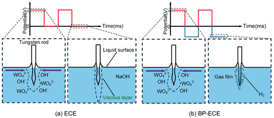
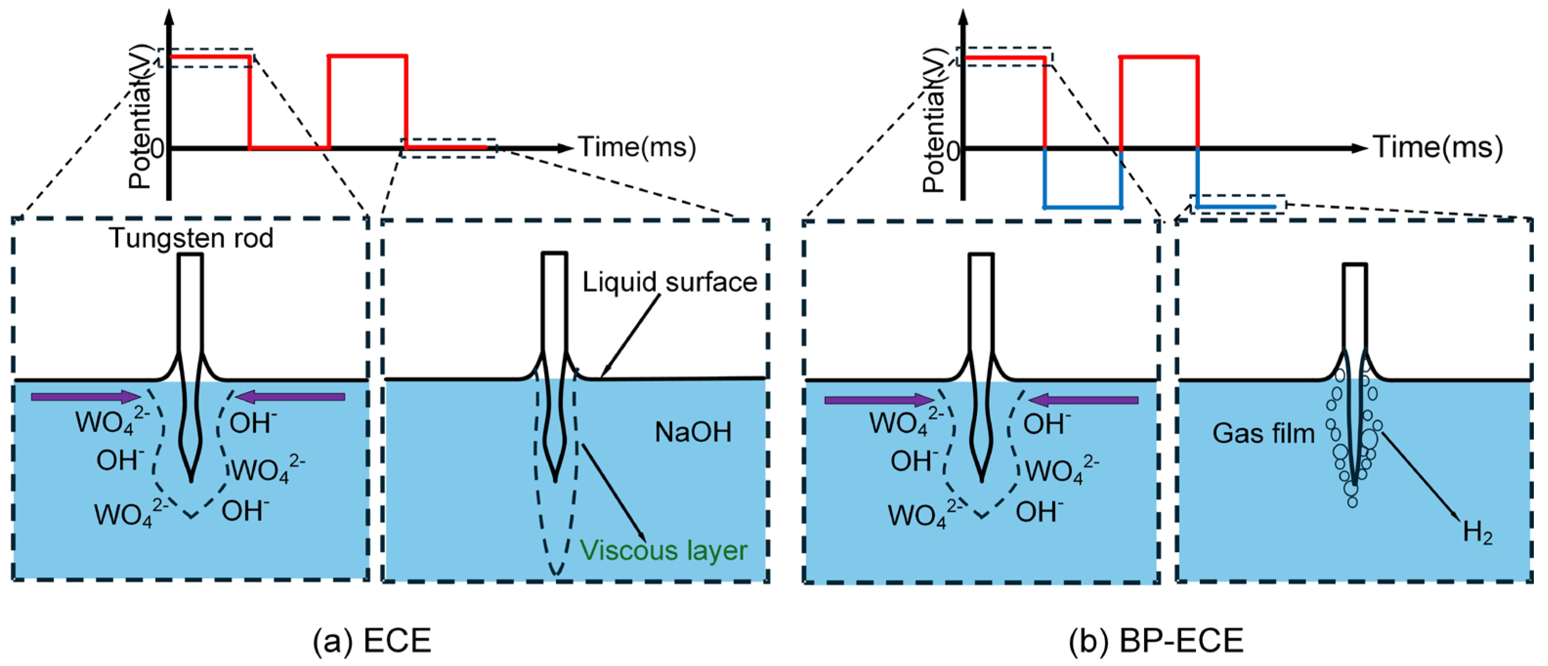
As shown in Figure 1a, in conventional electrochemical etching (ECE), the viscous layer generated on tungsten rods during positive pulse dissolution is mainly composed of negatively charged tungstate ions. These ions repel hydroxide ions, thereby hindering the subsequent etching process. The shuttle-shaped viscous layer thins near the liquid surface, increasing the local etching rate. Meanwhile, the viscous layer contracts at the lower end of the tungsten rod, and the electric field concentrates at the rod tip, which also accelerates the local etching rate. The combined effect of these two regions with enhanced etching ultimately yields the shuttle-shaped tungsten micro-rod. By contrast, as shown in Figure 1b, in bipolar pulse electrochemical etching (BP-ECE), bubbles generated by cathodic hydrogen evolution during negative pulses break through the viscous layer and disturb the electrolyte. This allows fresh electrolyte to recontact the tungsten rod surface and restore the etching efficiency and consistency. The alternating application of positive and negative pulses realizes the high-efficiency etching of tungsten micro-rods.
Figure 1.
Schematic diagram of conventional electrochemical etching and bipolar pulse electrochemical etching of a tungsten micro-rod. (a) ECE. (b) BP-ECE.
In BP-ECE, a tungsten rod is immersed in NaOH electrolyte. In the positive pulse, the rod acts as the anode, and metallic tungsten is oxidized to soluble tungstate ions. During the negative pulse, the tungsten rod serves as the cathode, where the hydrogen evolution reaction primarily occurs. The relevant electrode reactions are as follows:
Anode oxidation reaction:
W + 8OH− − 6e− → WO42− + 4H2O
Cathode reduction reaction:
2H2O + 2e− → H2↑ + 2OH−
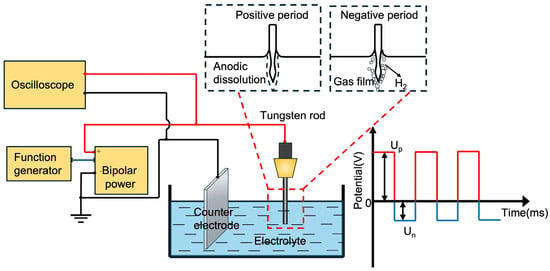
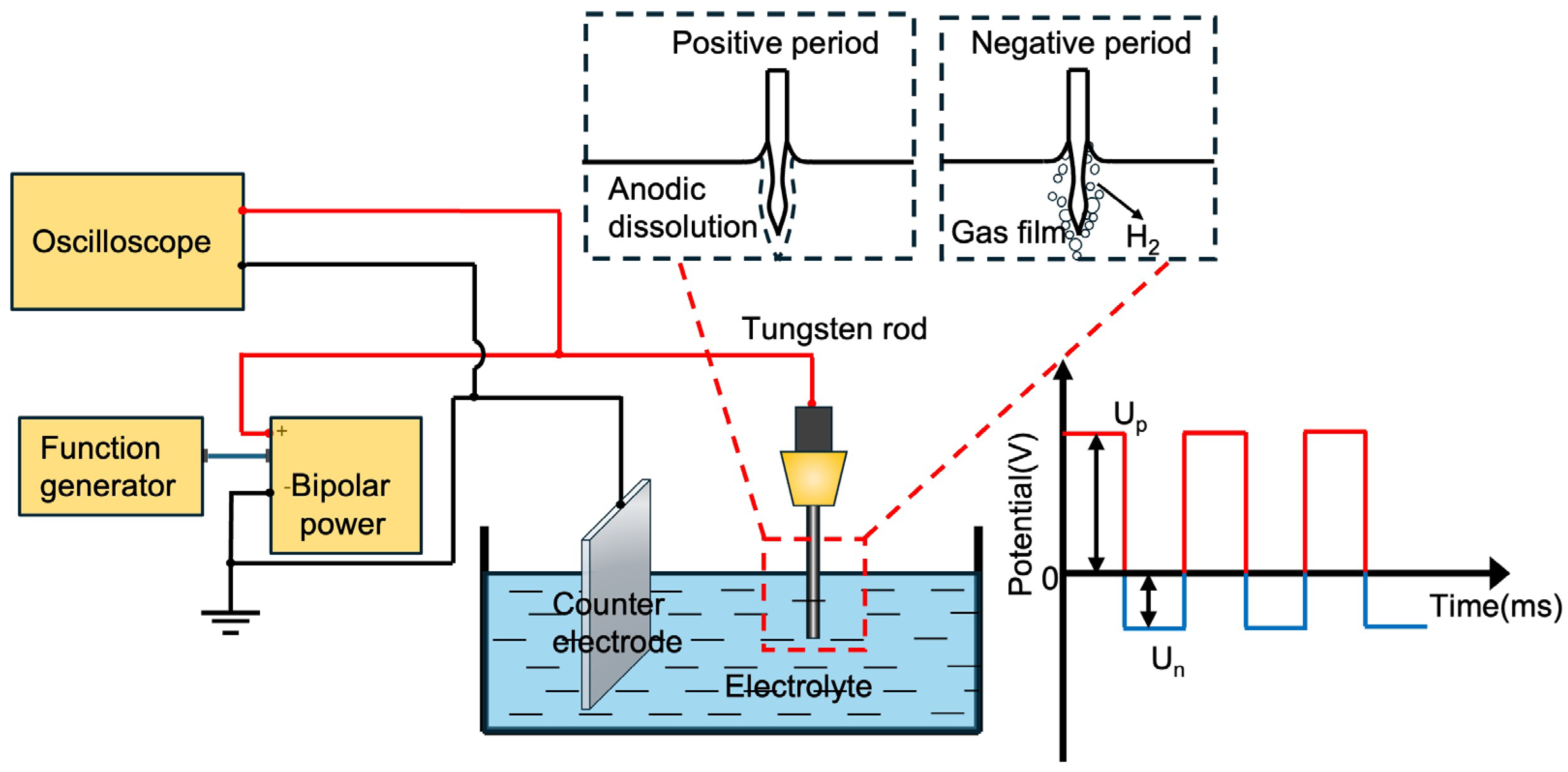
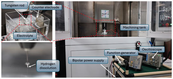
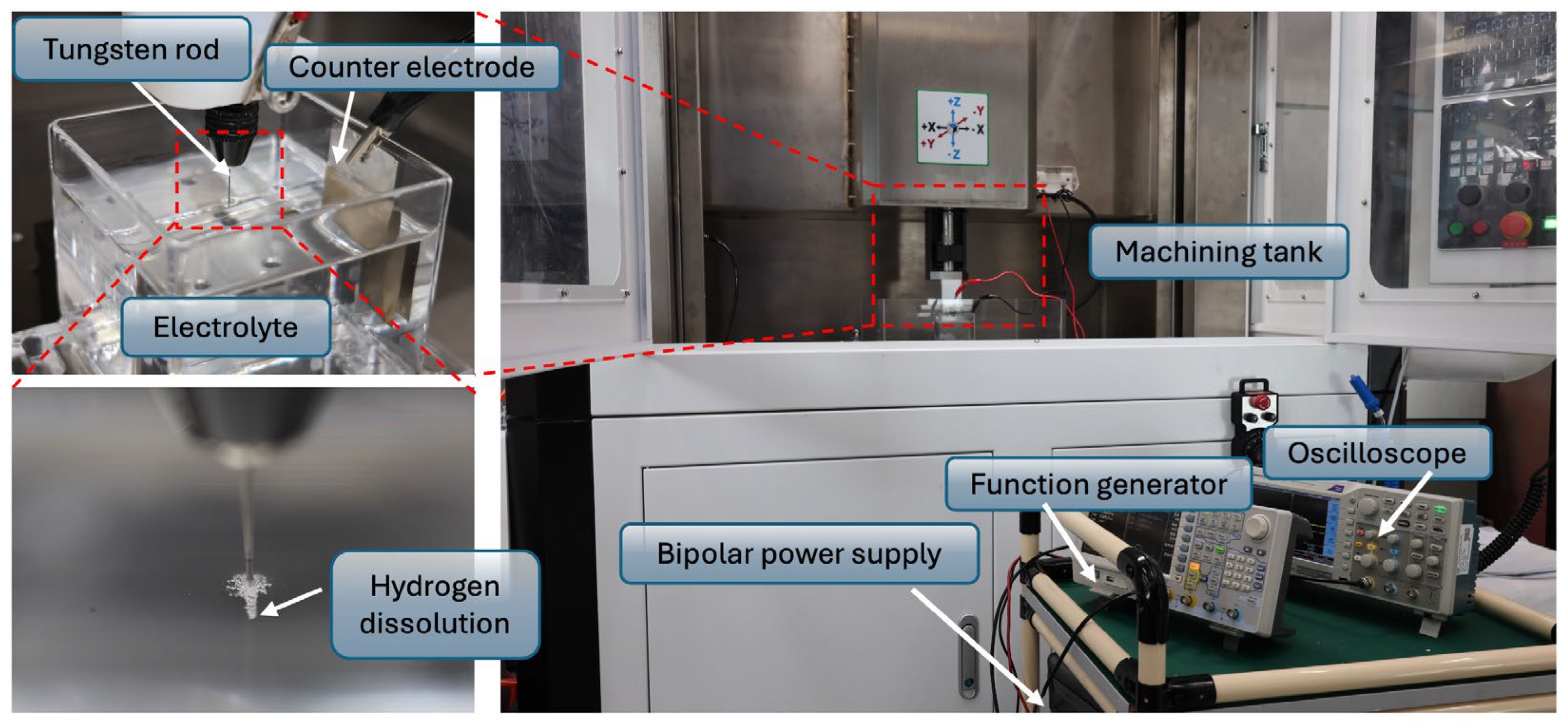
In this experiment, a bipolar pulse power supply with independently adjustable positive and negative duty cycles was employed. Figure 2 presents the schematic diagram of the experimental setup for BP-ECE of tungsten rods, and Figure 3 shows the practical machining scenario. A precision electrochemical machining tool (ECM205, Z-Yang, Shenzhen, China) was adopted to precisely control the immersion depth and position of tungsten rods. A screw-in fixture was mounted on the central spindle of the machine tool to ensure the vertical immersion of tungsten rods, and a water tank was placed beneath the spindle to serve as the electrolyte cell. A function generator (DG4162, Rigol, Suzhou, China) was used to output bipolar pulse waveforms, which were amplified by a power amplifier (FPA101, FeelElec, Zhengzhou, China) before application. Voltage and current signals during the machining process were captured by a voltage probe (TPP0200B, Tektronix, OR, USA) and a current probe (CP8030B, Cybertek, Shenzhen, China), and dynamically displayed on a digital oscilloscope (TBS 1152B, Tektronix, OR, USA). High-purity tungsten rods with a diameter of 300 µm were used as workpieces, and a platinum sheet with dimensions of 50 mm × 30 mm × 0.2 mm served as the counter electrode. In the initial state, the tungsten rod was connected to the positive pole of the power supply and the platinum counter electrode was connected to the negative pole. The electrode gap was set to approximately 30 mm, and the immersion depth of the tungsten rod was 5 mm. The etching efficiency was quantitatively evaluated according to the length variation of tungsten rods with increasing etching time. Each experiment was repeated three times to ensure process reproducibility. The specific experimental conditions for BP-ECE of tungsten micro-rods are shown in Table 1. A single-lens reflex camera (R8, Canon, Tokyo, Japan) was employed to observe phenomena during the experimental process. The morphology of the tungsten rods was examined using an image measuring instrument (Newstandard 322pro, Serein, Shenzhen, China) and a scanning electron microscope (SEM, Crossbeam 350, Zeiss, Oberkochen, Germany), and energy-dispersive spectrometer (EDS) analysis was conducted on the black film.
Figure 2.
Schematic diagram of the experimental setup for BP-ECE.
Figure 3.
Experimental platform for tungsten micro-rods fabrication by BP-ECE.
Table 1.
Experimental conditions for BP-ECE of tungsten micro-rods.
3. Analysis of the Impact of Pulse Polarity Amplitude on BP-ECE
3.1. Effect of Positive Pulse Amplitude
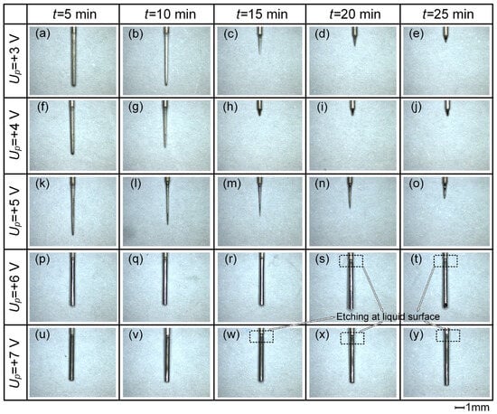
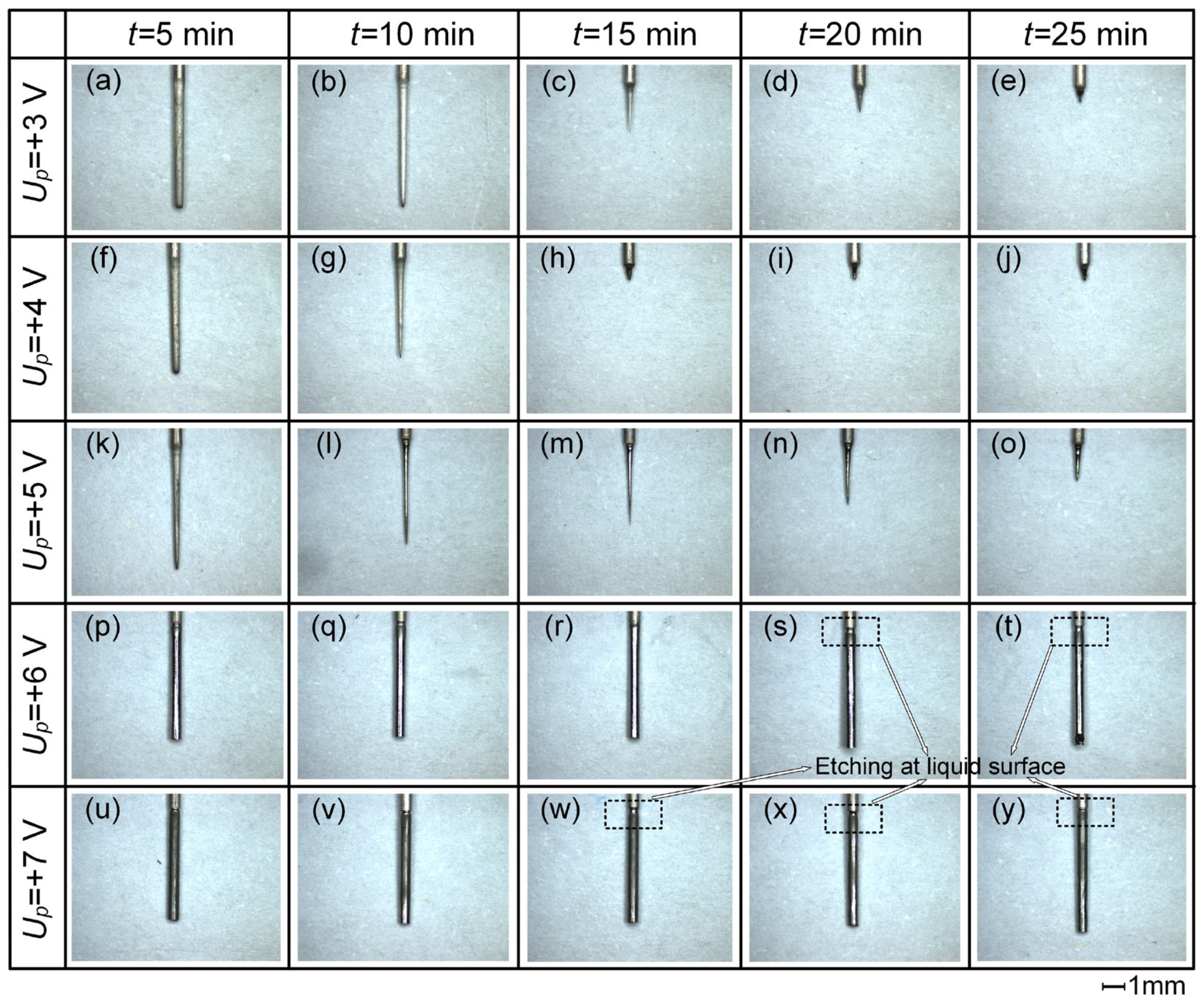
To explore the influence mechanism of positive polarity amplitude on the dissolution behavior and morphological consistency of tungsten micro-rods in BP-ECE, experiments were designed with a fixed negative voltage (Un = −2 V) and variable positive voltages (Up = +3 V, +4 V, +5 V, +6 V, and +7 V). The etched morphology of tungsten micro-rods was analyzed, and the corresponding results are presented in Figure 4 and Figure 5.
Figure 4.
Etched morphology of tungsten micro-rods under different positive pulse amplitudes. (a–e) Up = +3 V. (f–j) Up = +4 V. (k–o) Up = +5 V. (p–t) Up = +6 V. (u–y) Up = +7 V.
Figure 5.
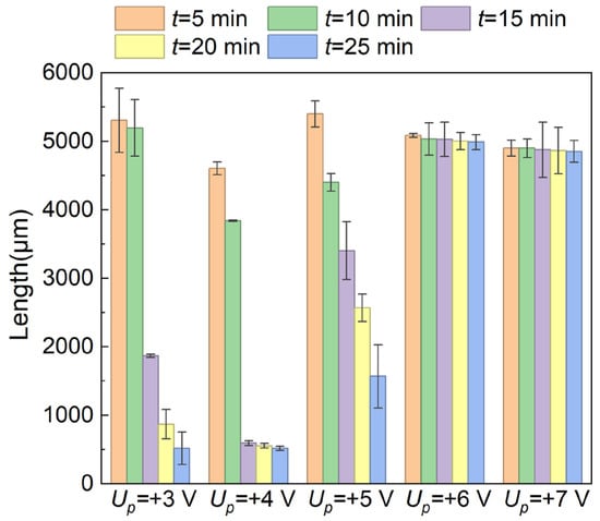
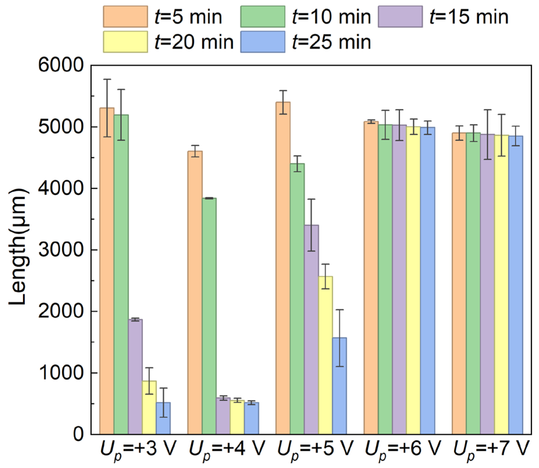
Variation in tungsten micro-rods’ length under different positive pulse amplitudes.
The machined results indicate that the etching efficiency of tungsten micro-rods increases with the rise in positive pulse amplitude at Up = +3 V and Up = +4 V. For instance, after 10 min of etching, the tungsten micro-rod length decreases from 5150 μm at Up = +3 V (Figure 4b) to 3760 μm at Up = +4 V (Figure 4g). Furthermore, the tungsten micro-rod is almost completely etched after 25 min at Up = +3 V (Figure 4e), whereas complete etching is achieved within 15 min at Up = +4 V (Figure 4h). However, a further increase in positive voltage leads to a reduction in etching efficiency. At Up = +5 V, the tungsten micro-rod retains a significantly longer length under the same etching duration compared with the case at Up = +4 V, indicating a lower material removal rate. When the positive voltage increases to Up = +6 V and Up = +7 V, the material removal amount is remarkably reduced. The tungsten micro-rods basically maintain their original cylindrical shape, with the rod length remaining approximately 5 mm (Figure 5), consistent with the immersion depth. In addition, a dark film is observed covering the micro-rod surface under high positive voltage conditions.
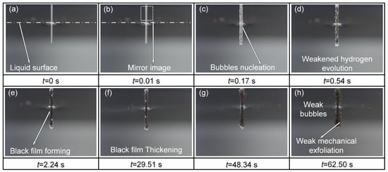
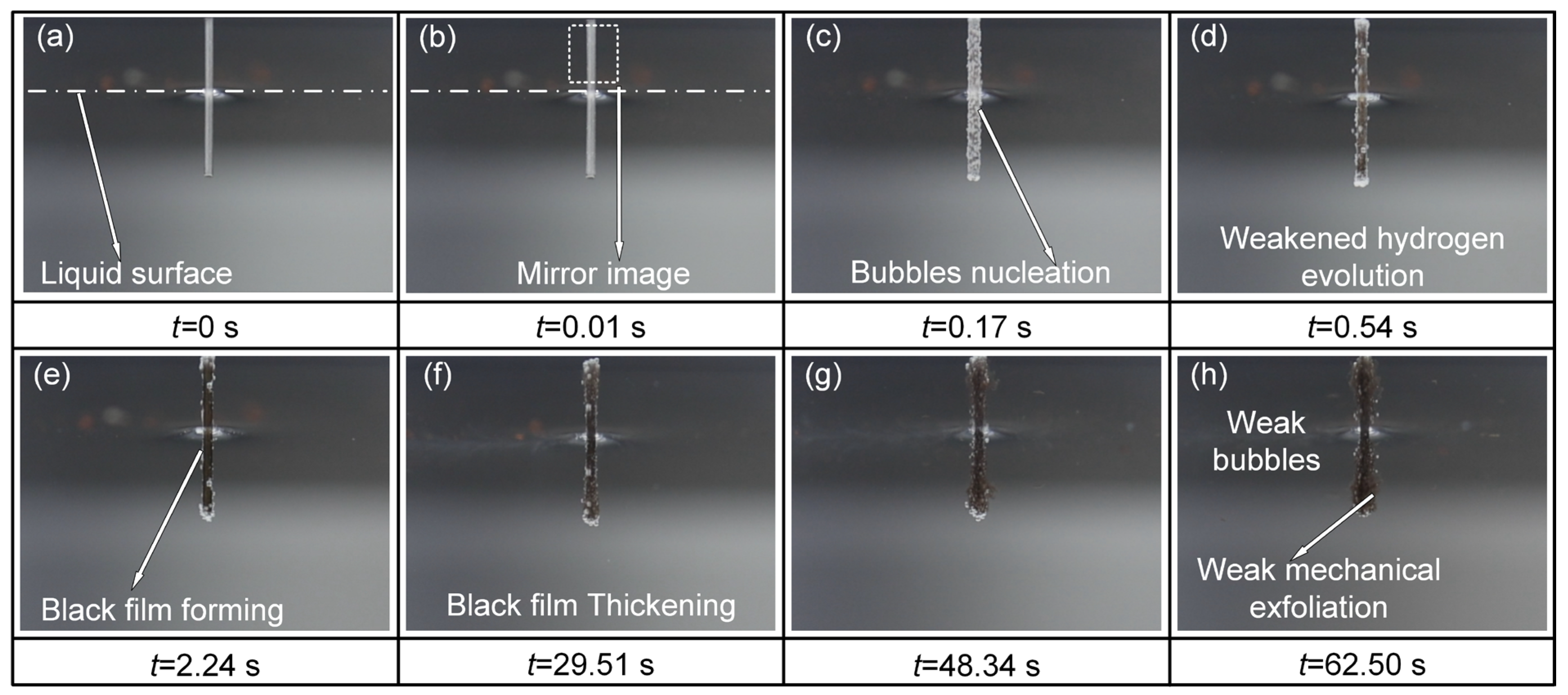
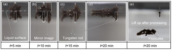
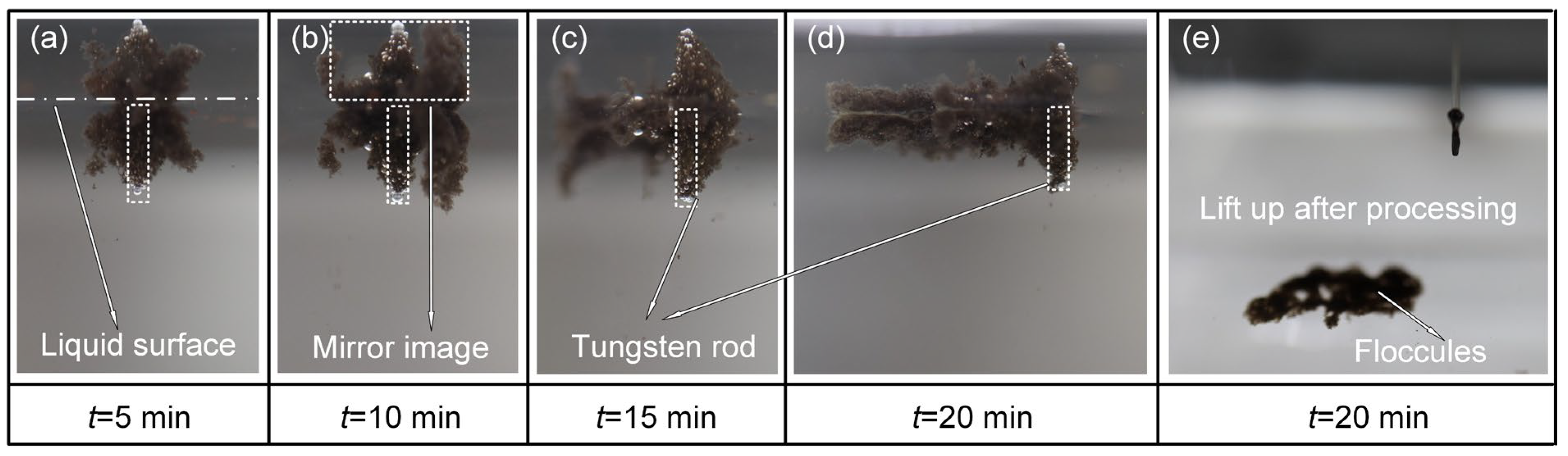
To clarify the formation mechanism of the black film, the machining phenomena at Up = +6 V were systematically observed. As shown in Figure 6, at the initial reaction stage, gas nucleation and precipitation occur on the tungsten micro-rod surface. Subsequently, surface tungsten oxides are reduced at t = 0.54 s, accompanied by a weakened hydrogen evolution reaction [24]. An obvious black film forms on the tungsten micro-rod surface at t = 2.24 s (Figure 6e), and the film thickness gradually increases over time before eventual peeling off (Figure 6h). The peeling process of the black film is illustrated in Figure 7. Significant film peeling is observed at t = 5 min, generating abundant black floccules that continuously accumulate and float upward to the electrolyte surface with prolonged machining time.
Figure 6.
Black film formation on tungsten micro-rod surface at Up = +6 V. (a) t = 0 s. (b) t = 0.01 s. (c) t = 0.17 s. (d) t = 0.54 s. (e) t = 2.24 s. (f) t = 29.51 s. (g) t = 48.34 s. (h) t = 62.50 s.
Figure 7.
Black film peeling off the tungsten micro-rod surface at Up = +6 V. (a) t = 5 min. (b) t = 10 min. (c) t = 15 min. (d) t = 20 min. (e) t = 20 min, lift up after processing.
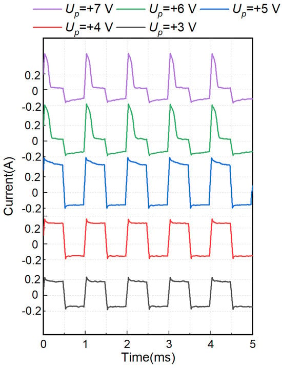
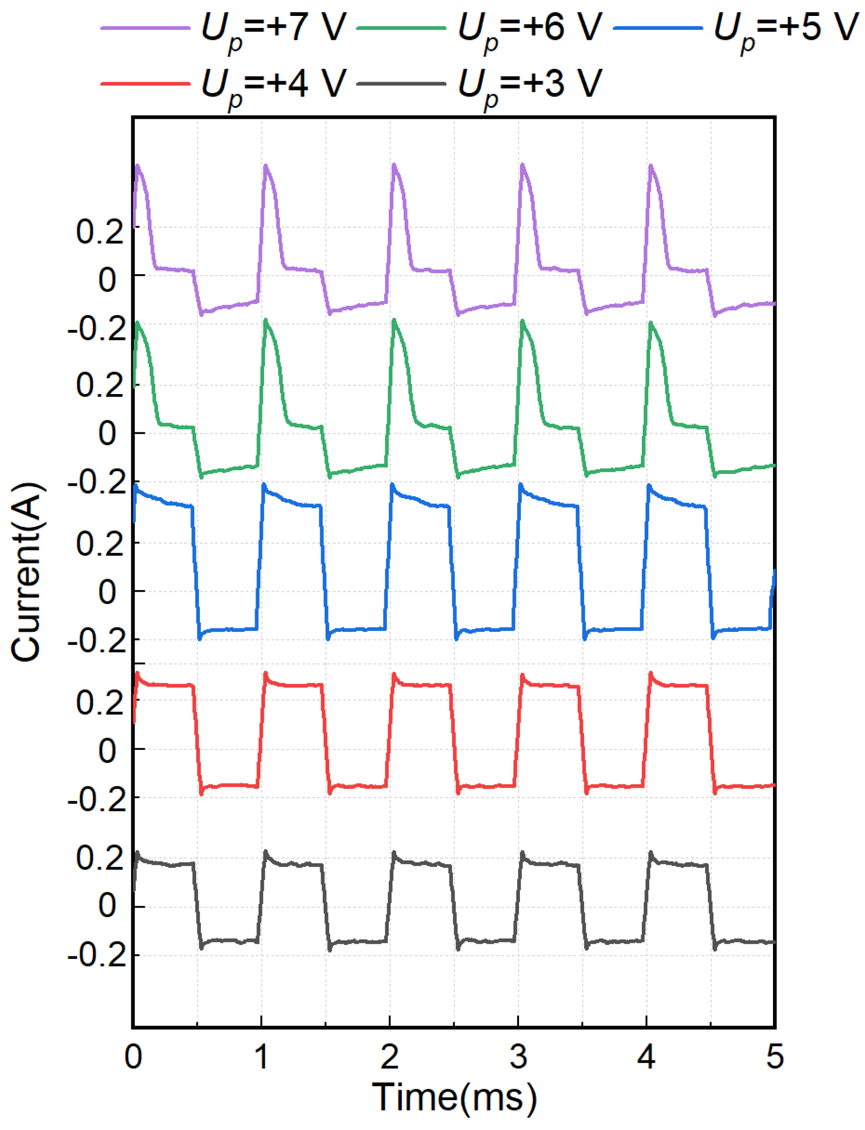
Furthermore, current signals during machining were analyzed to reveal the etching mechanism of tungsten micro-rods and the influence of black films under different positive voltages (Figure 8). At Up = +3 V and Up = +4 V, the current waveforms present a regular square-wave shape, indicating stable etching processes. Bubble generation exerts no substantial disturbance on machining, and no black film is formed. At Up = +5 V, the positive current waveform exhibits a slight sloped decline and deviates from the standard square wave. When Up increases to +6 V and +7 V, distinct current spikes appear at the pulse edges and decay rapidly, demonstrating that effective anodic current cannot be sustained, which accounts for the reduced machining efficiency. This rapid current decay originates from the generation of the black film on the tungsten surface at the onset of the pulse. The newly formed black layer acts as a barrier and suppresses the anodic current immediately after the pulse starts. The current waveform analysis is consistent with the morphological results in Figure 4, confirming that the formation of the black film observed in Figure 6 is the fundamental cause of the decreased anodic current.
Figure 8.
Current waveforms under different positive pulse amplitudes.
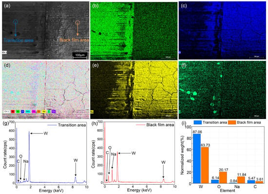
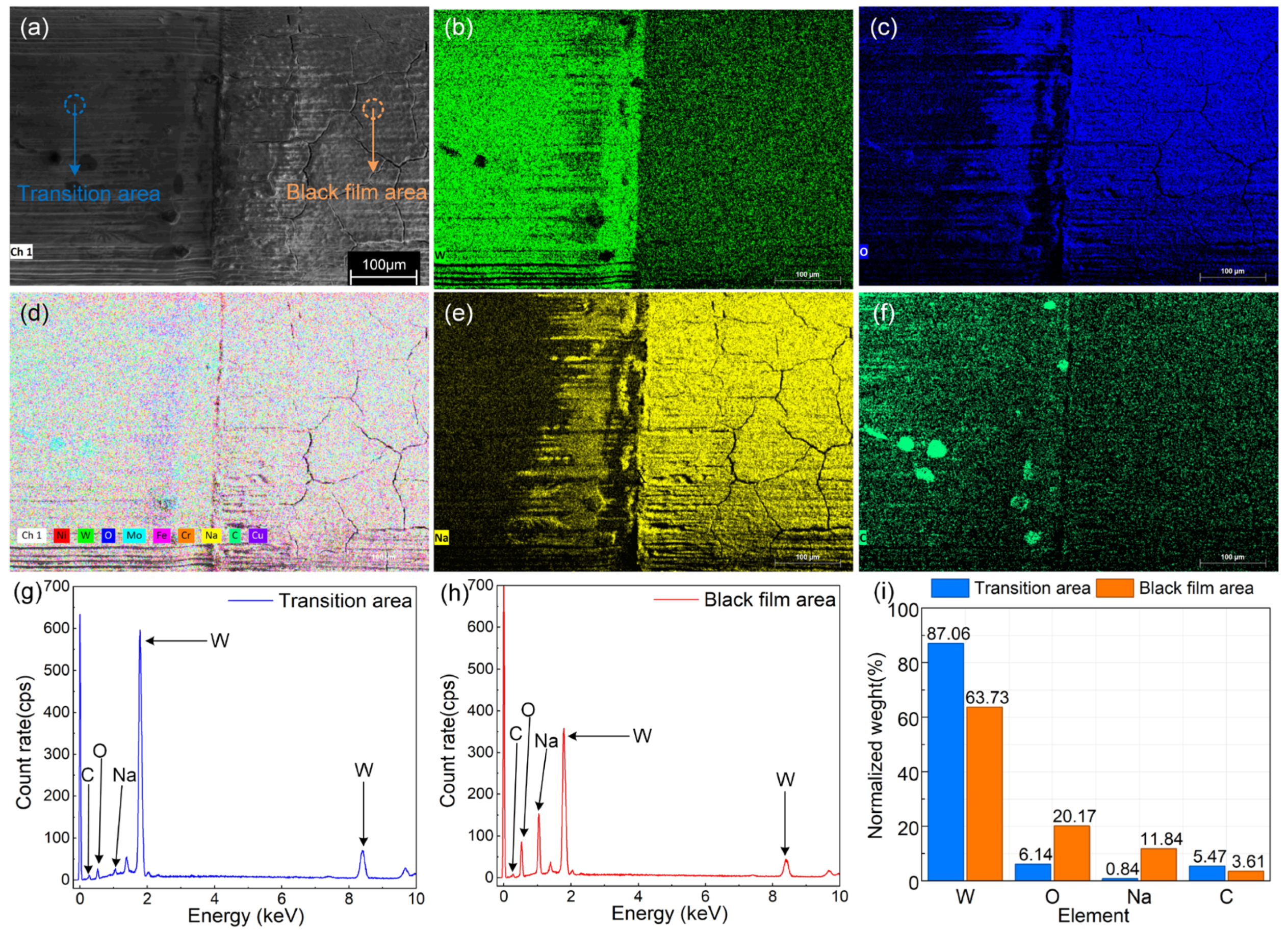
To analyze the composition of the black film, EDS analysis was performed on both the transition area and the black film area, with results shown in Figure 9. According to the EDS mapping results (Figure 9a–f), O and Na are significantly enriched in the area covered by the black film, while the W signal is relatively stronger in the transition area, indicating that the primary component of the black film is tungsten oxide, along with a small amount of deposited sodium complexes. C mainly originates from contamination during the analysis process. Furthermore, point EDS analysis of the transition area and black film area (Figure 9g–i) reveals that, compared to the transition area, the mass percentages of O and Na in the black film region increase from 6.14% and 0.84% to 20.17% and 11.84%, respectively, while W decreases from 87.06% to 63.73%. The EDS results confirm that the main component of the black film is tungsten oxide. Additionally, the presence of numerous micro-cracks on the black film suggests that significant gas evolution on the tungsten micro-rod could disrupt the black film, causing it to peel off.
Figure 9.
EDS analysis results in the transition area and the black film area. (a) SEM image. (b) W element. (c) O element. (d) Mapping results. (e) Na element. (f) C element. (g) Point analysis of transition area. (h) Point analysis of black film area. (i) Elemental content comparison.
3.2. Effect of Negative Pulse Amplitude
Based on the above investigations on positive pulse amplitude, Up = +5 V is determined to enable stable etching of tungsten micro-rods without the formation of obstructive black films. On this basis, the positive voltage was fixed at Up = +5 V, and the effect of negative-pulse assistance on tungsten micro-rod etching was explored by varying the negative polarity intensity. The negative pulse amplitude Un was set to −1 V, −2 V, and −3 V, and unipolar pulse machining (Un = 0 V) was adopted as the control group. The hydrogen evolution behavior, evolution of surface black films, submerged etching morphology, and machining efficiency were systematically investigated.
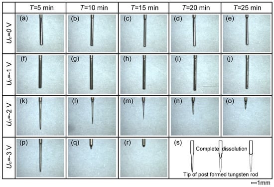
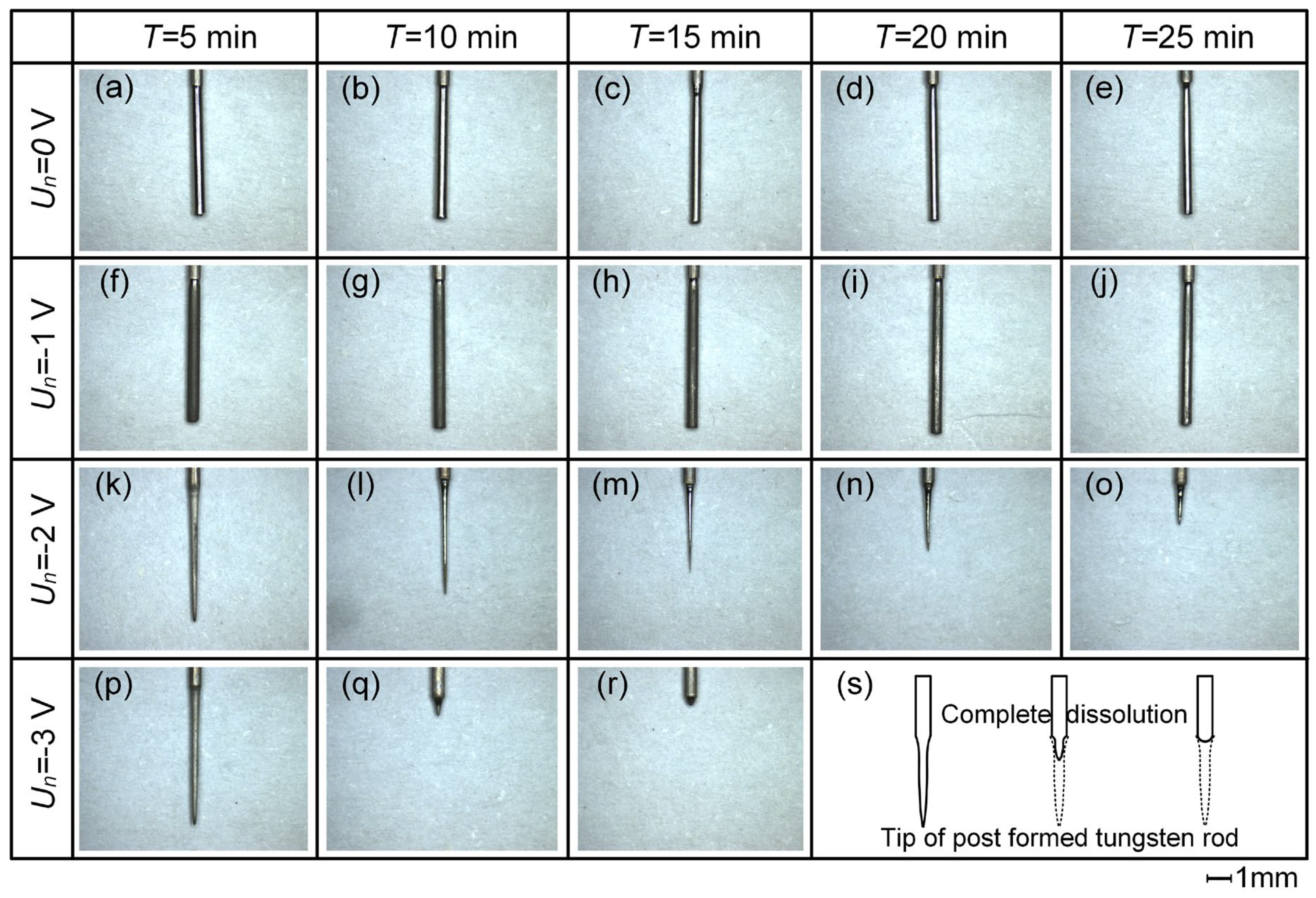
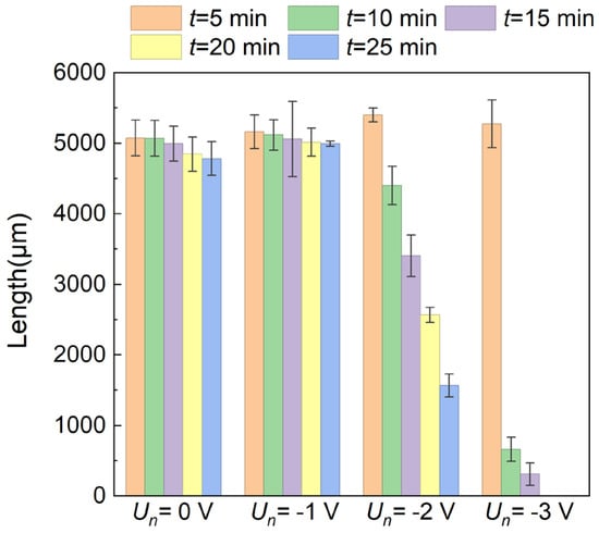
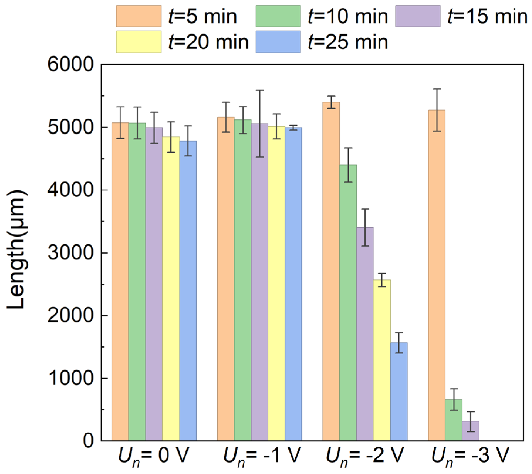
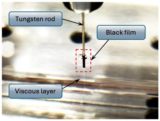
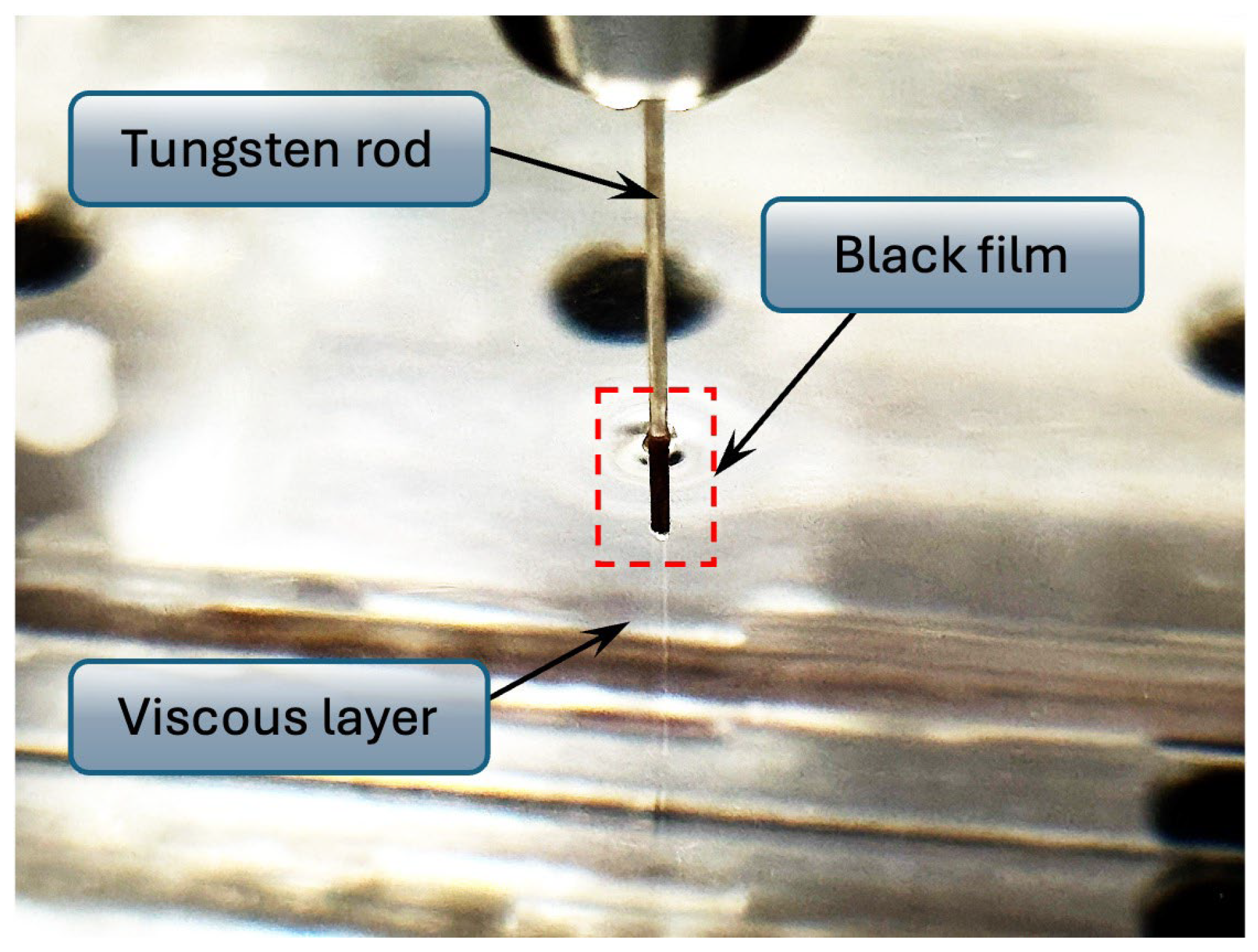
As shown in Figure 10 and Figure 11, the machined results show that the tungsten micro-rod surface remains bright and clean at Un = 0 V, whereas obvious black deposits emerge on the rod surface at Un = −1 V. The tungsten micro-rods exhibit similar lengths under Un = 0 V and Un = −1 V, both retaining the initial length of approximately 5 mm with low etching efficiency (Figure 11). Combined with the morphological characteristics in Figure 10f and Figure 12, black films are formed on the tungsten micro-rod surface. This indicates that insufficient negative pulse amplitude fails to facilitate the etching process; instead, it deteriorates the interfacial conditions, hinders charge transfer, and reduces the etching efficiency.
Figure 10.
Etched morphology of tungsten micro-rods under different negative pulse amplitudes. (a–e) Un = 0 V. (f–j) Un = −1 V. (k–o) Un = −2 V. (p–s) Un = −3 V.
Figure 11.
Variation in tungsten micro-rods length under different negative pulse amplitudes.
Figure 12.
Viscous layer and black film generated during the etching process.
At Un = −2 V, intensive and dense hydrogen bubbles are generated during the negative pulse stage. This necking phenomenon occurs at Un = 0 V because a viscous layer forms on the tungsten micro-rod surface. The viscous layer is thinner near the liquid surface, which increases the local etching rate and induces necking. In contrast, at Un = −2 V, under negative polarity, bubbles generated on the tungsten surface suppress the formation of the viscous layer, so no necking is observed. The etching region expands from the liquid level to the entire submerged section, and the tungsten micro-rod forms a stable tapered tip along the submerged segment with a well-linear length variation. Additionally, no black deposits are observed on the rod surface. Therefore, Un = −2 V is identified as the optimal negative pulse amplitude that balances machining efficiency and surface morphology. Further increasing the negative amplitude to Un = −3 V induces violent hydrogen evolution. Massive bubbles peel off the black film, which subsequently aggregate and float to the electrolyte surface, leading to a significantly enhanced tungsten dissolution rate. As illustrated in Figure 10 and Figure 11, at Un = −3 V, most of the tungsten rod is dissolved after 10 min of machining, leaving only a short residual tip, which fails to form a qualified slender micro-rod.
The negative pulse amplitude exhibits an evident window effect on etching performance. At Un = −1 V, insufficient hydrogen evolution cannot eliminate the surface black film, resulting in lower machining efficiency than the unipolar machining condition. The optimal comprehensive machining performance, including high efficiency and superior surface quality, is achieved at Un = −2 V. In contrast, excessive negative amplitude (Un = −3 V) causes over-fast material removal and uncontrollable micro-rod morphology.
4. Analysis of the Impact of Pulse Time Domain on BP-ECE
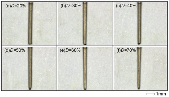
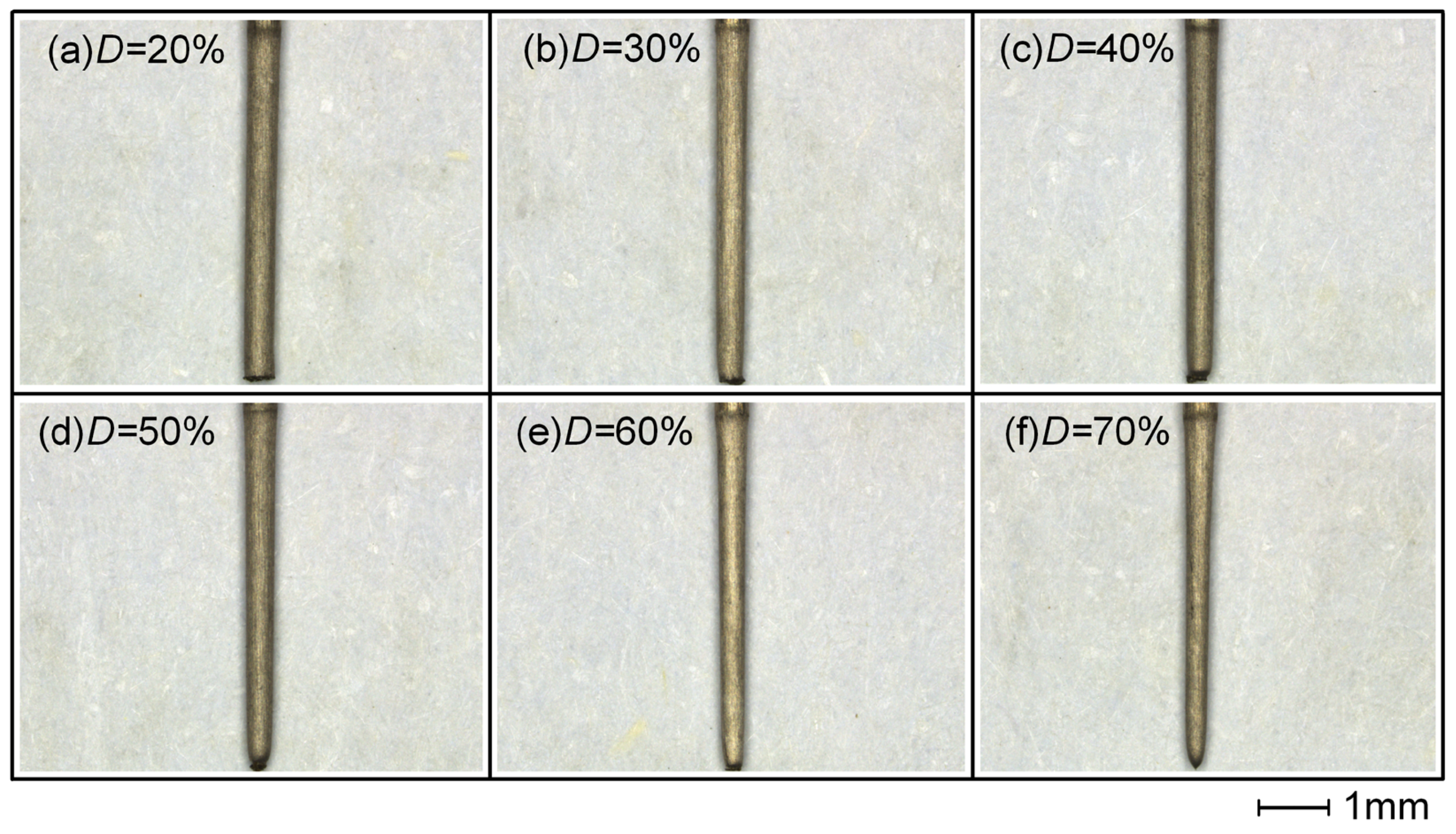
To explore the effect of pulse time domain on tungsten micro-rod etching, the influence of positive pulse duty cycle on etching efficiency and black film evolution was investigated. The voltage was fixed at Up = +3 V, Up = +5 V, and Un = −2 V. The positive duty cycle was set to 20%, 30%, 40%, 50%, 60%, and 70%, and each group was etched for 5 min.
As shown in Figure 13, at a low forward voltage of Up = 3 V, the etching amount of tungsten material is generally small. Under this condition, no black film coverage was observed at any duty cycle, and hydrogen evolution was clearly evident during the experiment. At low forward voltages, the oxidation degree on the tungsten surface is weak, and within the examined range of duty cycles, the interfacial disturbances caused by hydrogen evolution are sufficient to suppress the formation of black films.
Figure 13.
Etched morphology of tungsten micro-rods under different positive pulse duty cycles at Up = +3 V. (a) D = 20%. (b) D = 30%. (c) D = 40%. (d) D = 50%. (e) D = 60%. (f) D = 70%.
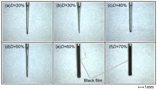
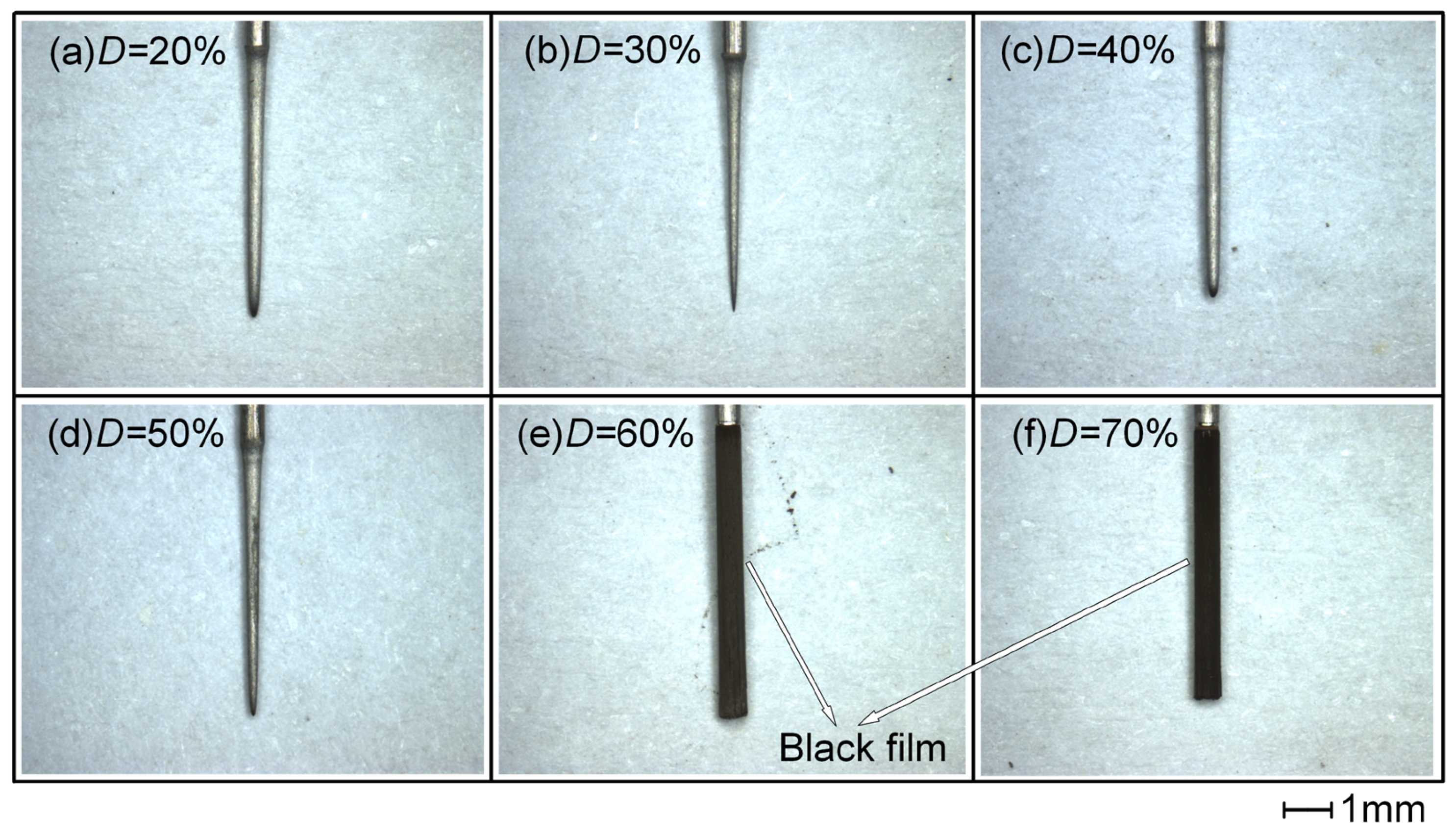
In addition, as shown in Figure 14, at a high forward voltage of Up = 5 V, significant material removal and bright surfaces are achieved at duty cycles D ≤ 50%. In contrast, dense black films fully cover the micro-rod surface at D = 60% and 70%, which drastically suppresses material removal. At low positive duty cycles, the prolonged duration of negative pulses generates abundant hydrogen bubbles on the tungsten surface, which inhibits black film formation and improves both etching efficiency and surface quality. However, high positive duty cycles remarkably reduce hydrogen production. Insufficient bubble agitation fails to strip black film, leading to reduced etching efficiency.
Figure 14.
Etched morphology of tungsten micro-rods under different positive pulse duty cycles at Up = +5 V. (a) D = 20%. (b) D = 30%. (c) D = 40%. (d) D = 50%. (e) D = 60%. (f) D = 70%.
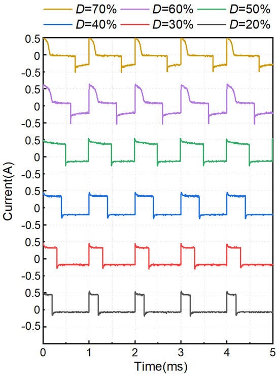
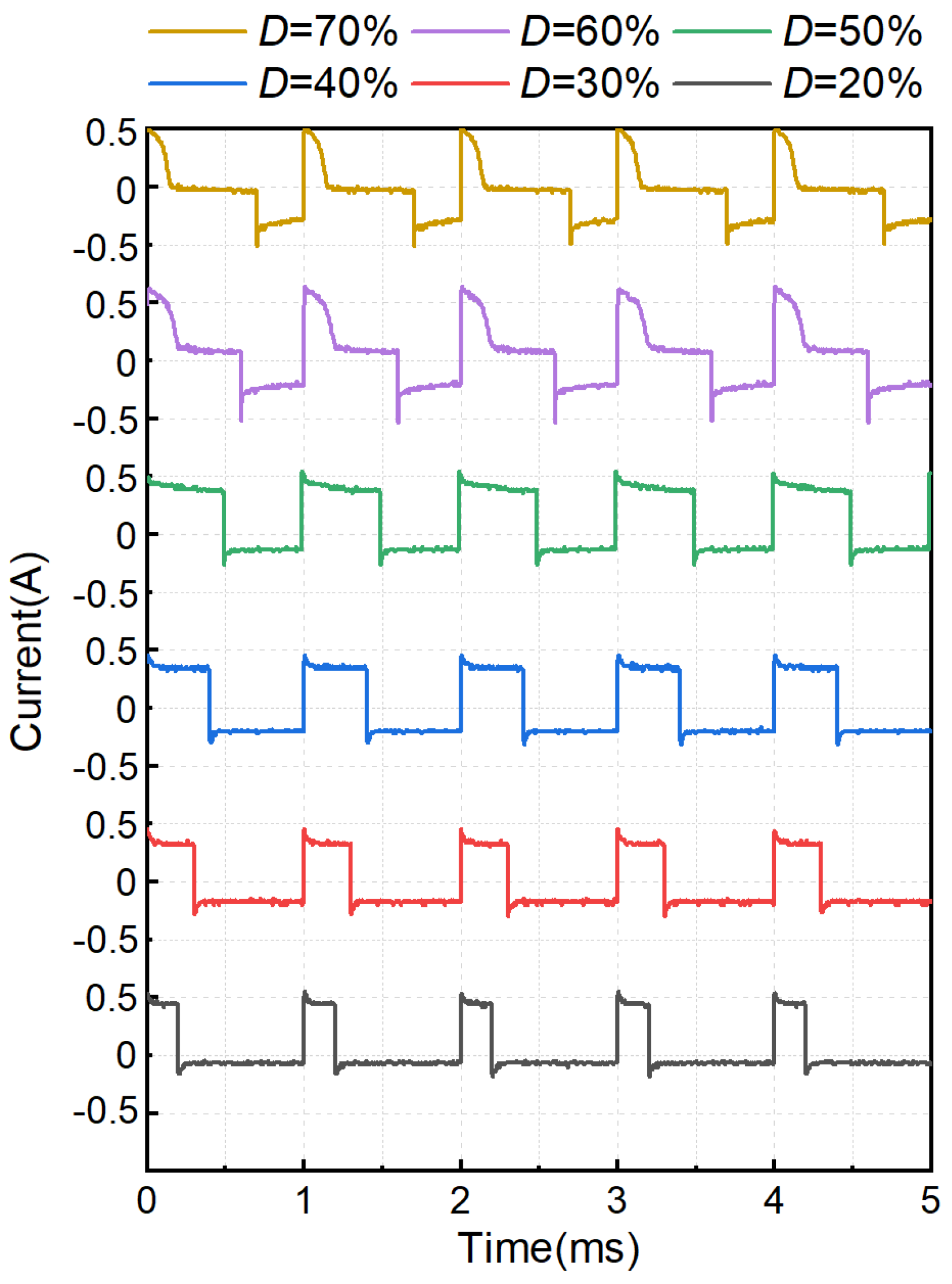
Current waveforms under different positive duty cycles are displayed in Figure 15. Regular square-wave current profiles are maintained at D ≤ 50%, demonstrating stable etching processes. By contrast, at D = 60% and 70%, the current rises sharply at the initial pulse stage and then decays obviously, indicating that the formed black film significantly hinders anodic dissolution. This electrical response is highly consistent with the morphological results in Figure 14. Therefore, in BP-ECE, properly allocating the time domain duration of positive and negative pulses is crucial to prevent the formation of black films that hinder processing.
Figure 15.
Current waveforms under different positive pulse duty cycles.
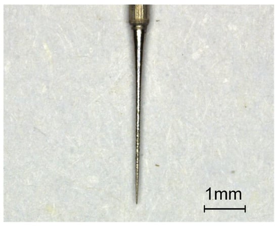
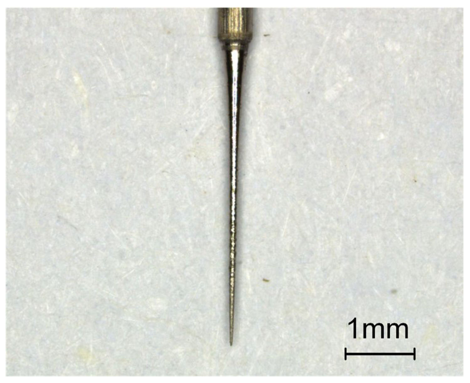
Based on the above experimental results, a tungsten probe was etched for 11 min using parameters of Up = 5 V, Un = −2 V, and D = 50%. The machining results are shown in Figure 16. Measurements indicate that the tungsten probe has a length of approximately 4.2 mm, a tip diameter of about 10 µm, and an overall conical profile, with no obvious local necking phenomenon.
Figure 16.
High aspect ratio tungsten probe processed with optimized parameters.
5. Mechanism of Negative Pulse Action and Black Film Evolution
The promotional mechanism of negative pulses on the etching process can be summarized into three aspects. First, hydrogen evolution agitation enhances mass transfer. During negative pulse stages, the tungsten micro-rod acts as the cathode and undergoes hydrogen evolution. The generation, growth, and detachment of bubbles intensely disturb the near-wall electrolyte, continuously scouring and destroying the viscous layer and black film formed during anodic dissolution. This enables timely replenishment of fresh electrolyte and effective discharge of dissolved products, alleviating concentration polarization and improving the anodic dissolution rate. Second, interfacial charge neutralization occurs. The reverse charges provided by negative pulses neutralize the positive charges stored in the electric double layer, accelerate double-layer discharge and depolarization, and reduce the residual polarization voltage during pulse intervals. Third, the forming consistency is improved. Material removal in conventional ECE is concentrated near the liquid level, and micro-rod formation relies heavily on local necking and fracture at the air-liquid interface. By contrast, the submerged section of the tungsten micro-rod presents a uniform tapered profile in BP-ECE. The machining morphology is no longer limited to localized necking near the liquid surface, indicating reduced sensitivity to interfacial condition fluctuations and improved batch machining consistency.
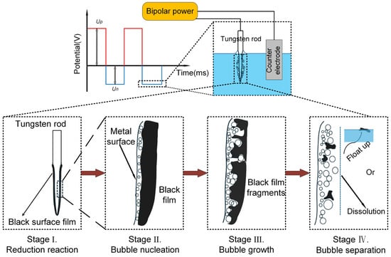
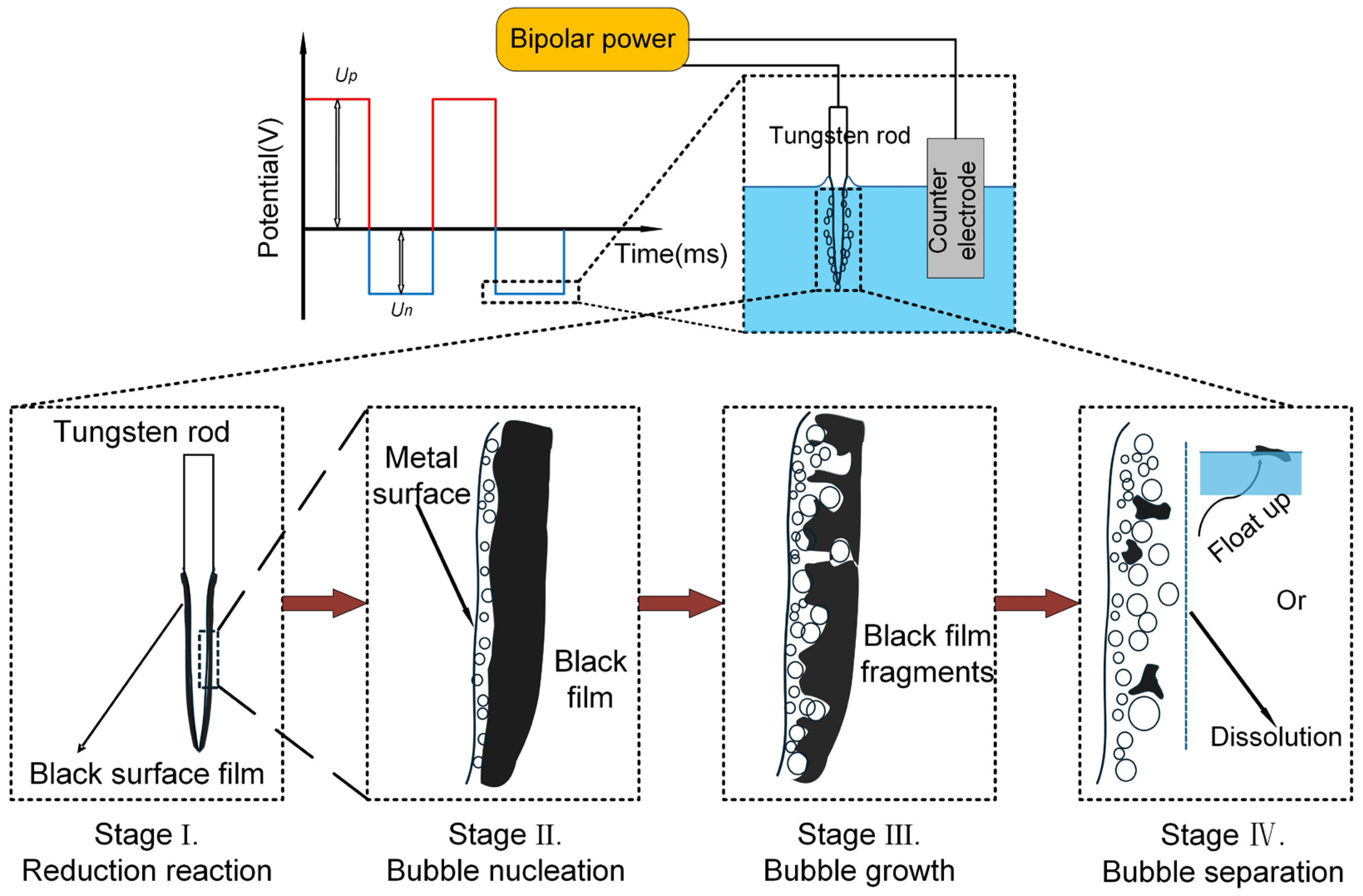
To elaborate on the formation and peeling mechanisms of the black film, four sequential interfacial evolution stages within one alternating positive–negative pulse cycle are schematically illustrated in Figure 17. The black film is primarily an oxide layer that has not been further dissolved or broken down. During the application of a positive pulse, tungsten oxidizes to form the intermediate compound WO3, which can subsequently convert into the soluble species WO42−. In Stage I, during the negative pulse phase, the balance between the formation and consumption of WO3 is disrupted, leading to the formation of a black film under specific conditions. In Stage II, hydrogen bubbles nucleate at the film substrate interface. Continuous hydrogen accumulation forms a gas cushion closely attached to the rod surface. The outer layer of the black film reacts with the surrounding electrolyte, leading to a loose film structure and flocculent deposits, which significantly weaken the bonding force between the film and the tungsten substrate. In Stage III, when the bubbles grow to a critical size, the combined buoyancy and internal pressure overcome the surface adhesion force, driving bubble detachment and upward escape. Bubble separation induces intense local electrolyte disturbance and microconvection, accelerating the diffusion of tungstate ions while replenishing fresh hydroxide ions to the electrode surface. At this stage, the black film becomes fragile and nearly ruptures. In Stage IV, bubble detachment imposes a mechanical stripping effect on the loose black film, resulting in complete film rupture. The exposed fresh tungsten metal provides a clean reaction interface for uniform anodic dissolution in the subsequent positive pulse cycle.
Figure 17.
Schematic diagram of the formation and peeling mechanism of black film.
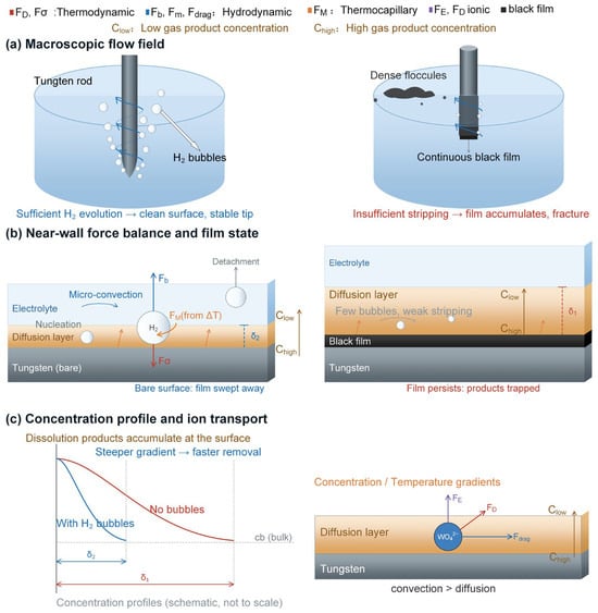
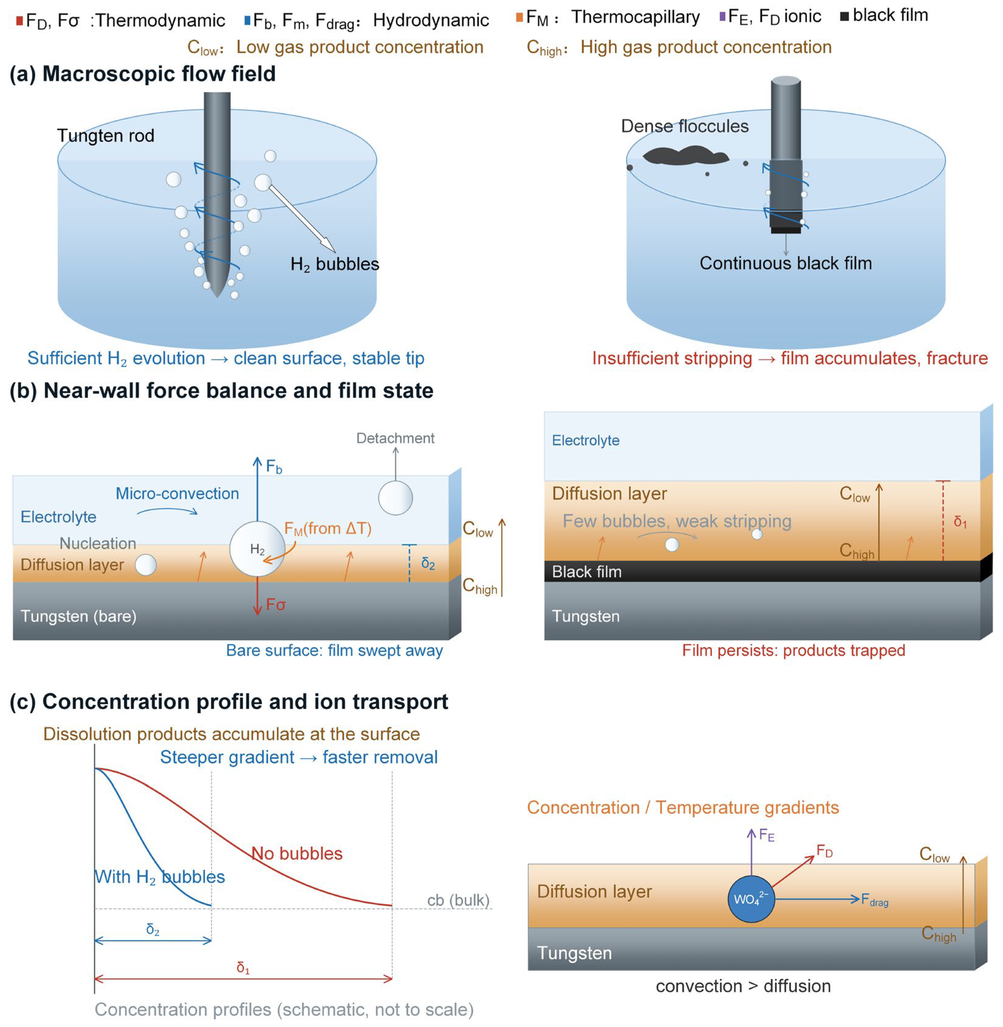
To further illustrate the mass transfer enhancement mechanism induced by hydrogen evolution, Figure 18a schematically compares the macroscopic flow fields under sufficient and insufficient hydrogen evolution conditions. During negative pulse polarization, the tungsten rod serves as the cathode for the hydrogen evolution reaction. Bubbles nucleate, grow, and detach along the rod surface, forming a continuous bubble plume. The upward floating plume drives the near-wall electrolyte to rise, enabling the replenishment of fresh electrolyte. Sufficient hydrogen evolution generates a vigorous bubble plume, contributing to a bright machining surface and high etching efficiency. In contrast, insufficient hydrogen evolution leads to sparse bubbles and weakened electrolyte convection, resulting in continuous accumulation of black films on the rod surface.
Figure 18.
Schematic diagram of hydrogen evolution-enhanced mass transfer. (a) Macroscopic flow field. (b) Near-wall force balance and film state. (c) Concentration profile and ion transport.
The mass transfer enhancement induced by bubbles is realized through fluid momentum transfer rather than direct ionic action. As shown in Figure 18b, bubbles in the near-wall region are subjected to the coupled effects of buoyancy, growth momentum force, and capillary anchoring force. Bubbles detach from the surface once the detaching forces exceed the anchoring force, and the bubble detachment radius and growth period determine the interface renewal frequency. In addition, Joule heat generated by the machining current induces a temperature gradient and tangential stress at the interface, driving the flow of near-wall liquid layers. Both buoyancy-driven convection and temperature-gradient-induced Marangoni convection have been observed in free surface electrochemical machining flow fields [25].
Moreover, as depicted in Figure 18c, the wake flow generated by bubble growth and detachment disturbs the near-wall liquid layer. Under sufficient hydrogen evolution, the thickness of the near-wall diffusion layer (viscous layer) decreases from δ1 (bubble-free condition) to δ2, maintaining a clean workpiece surface. By comparison, weak flow disturbance under insufficient hydrogen evolution preserves the original diffusion layer thickness δ1. The black film cannot be effectively stripped and thus continuously covers the micro-rod surface, reducing the etching efficiency.
6. Conclusions
This paper investigates the bipolar amplitude and time-domain characteristics in the BP-ECE of tungsten micro-rods, systematically analyzing the formation and evolution mechanisms of black films and their impact on the processing.
The positive pulse amplitude plays a critical role in determining the etching efficiency. Under relatively low positive polarity conditions, the material removal efficiency increases with the rise in positive voltage. Excessively high positive pulse amplitude induces the formation of black films on the electrode surface, which hinders anodic dissolution and thereby reduces the machining efficiency.
The negative pulse amplitude exhibits distinct process window characteristics. Insufficient negative pulse amplitude limits hydrogen evolution, preventing removal of black film at the micro-rod surface and suppressing etching efficiency. Conversely, overly strong negative pulses lead to excessively vigorous reactions, reducing the stability of micro-rod etching.
Pulse duty cycle controls the time domain of positive and negative pulses. A low positive duty cycle guarantees sufficient negative pulse action, effectively inhibiting black film generation. In comparison, a high positive duty cycle compresses the duration of negative pulses and weakens the hydrogen cleaning capability, leading to massive black film formation and consequent suppression of tungsten micro-rod etching.
For future research, the refined subdivision of negative polarity time domains and the motion control of the tungsten rod electrode, including rotational and lifting motions, may constitute the key to enhancing machining efficiency and precision.
Author Contributions
Conceptualization, C.W., K.J. and S.Z.; methodology, C.W., Y.L. and S.Z.; software, C.W., S.L. and Y.L.; validation, C.W., S.L. and Y.L.; formal analysis, C.W., J.W. and S.Z.; investigation, C.W. and S.Z.; resources, J.W., K.J. and S.Z.; data curation, C.W., S.L. and Y.L.; writing—original draft preparation, C.W., S.L. and S.Z.; writing—review and editing, C.W. and S.Z.; visualization, C.W., S.L. and Y.L.; supervision, J.W., K.J. and S.Z.; project administration, K.J. and S.Z.; funding acquisition, S.Z. All authors have read and agreed to the published version of the manuscript.
Funding
This research was funded by the Guangdong Basic and Applied Basic Research Foundation (grant numbers: 2023A1515110059), the Special Innovation Projects of Ordinary Colleges and Universities in Guangdong Province (grant numbers: 2024KTSCX254), the Shenzhen Science and Technology Innovation Commission (grant numbers: 20231127142945002), the Guangdong Province Science and Technology Innovation Strategy Special Foundation (grant number: pdjh2025bk380), Key Projects of Shenzhen University of Information Technology (grant number. SZIIT2025KJ006).
Institutional Review Board Statement
Not applicable.
Informed Consent Statement
Not applicable.
Data Availability Statement
The original contributions presented in this study are included in the article. Further inquiries can be directed to the corresponding author.
Conflicts of Interest
The authors declare no conflicts of interest.
References
- Han, W.; Kunieda, M. Fabrication of tungsten micro-rods by ECM using ultra-short-pulse bipolar current. CIRP Ann. 2017, 66, 193–196. [Google Scholar] [CrossRef] [Scilit]
- Choi, S.H.; Ryu, S.H.; Choi, D.K.; Chu, C.N. Fabrication of WC micro-shaft by using electrochemical etching. Int. J. Adv. Manuf. Technol. 2007, 31, 682–687. [Google Scholar] [CrossRef] [Scilit]
- Yu, Z.Q.; Wang, C.M.; Du, Y.; Thevuthasan, S.; Lyubinetsky, I. Reproducible tip fabrication and cleaning for UHV STM. Ultramicroscopy 2008, 108, 873–877. [Google Scholar] [CrossRef] [Scilit]
- Onikura, H.; Ohnishi, O.; Take, Y.; Kobayashi, A. Fabrication of micro carbide tools by ultrasonic vibration grinding. CIRP Ann. 2000, 49, 257–260. [Google Scholar] [CrossRef] [Scilit]
- Ohmori, H.; Katahira, K.; Uehara, Y.; Watanabe, Y.; Lin, W. Improvement of mechanical strength of micro tools by controlling surface characteristics. CIRP Ann. 2003, 52, 467–470. [Google Scholar] [CrossRef] [Scilit]
- Masuzawa, T.; Fujino, M.; Kobayashi, K.; Suzuki, T.; Kinoshita, N. Wire electro-discharge grinding for micro-machining. CIRP Ann. 1985, 34, 431–434. [Google Scholar] [CrossRef] [Scilit]
- Ho, K.H.; Newman, S.T.; Rahimifard, S.; Allen, R. State of the art in wire electrical discharge machining (WEDM). Int. J. Mach. Tools Manuf. 2004, 44, 1247–1259. [Google Scholar] [CrossRef] [Scilit]
- Koyano, T.; Sugata, Y.; Hosokawa, A.; Furumoto, T. Micro-electrical discharge machining of micro-rods using tool electrodes with high electrical resistivity. Precis. Eng. 2019, 55, 95–100. [Google Scholar] [CrossRef] [Scilit]
- Painuly, M.; Singh, R.P.; Trehan, R. Electrochemical machining and allied processes: A comprehensive review. J. Solid State Electrochem. 2023, 27, 3189–3256. [Google Scholar] [CrossRef] [Scilit]
- Kerfriden, S.; Nahlé, A.H.; Campbell, S.A.; Walsh, F.C.; Smith, J.R. Short CommunicationThe electrochemical etching of tungsten STM tips. Electrochim. Acta 1998, 43, 1939–1944. [Google Scholar] [CrossRef] [Scilit]
- Lim, Y.M.; Kim, S.H. An electrochemical fabrication method for extremely thin cylindrical micropin. Int. J. Mach. Tools Manuf. 2001, 41, 2287–2296. [Google Scholar] [CrossRef] [Scilit]
- Fan, Z.W.; Hourng, L.W.; Wang, C.Y. Fabrication of tungsten microelectrodes using pulsed electrochemical machining. Precis. Eng. 2010, 34, 489–496. [Google Scholar] [CrossRef] [Scilit]
- Chiou, Y.C.; Lee, R.T.; Chen, T.J.; Chiou, J.-M. Fabrication of high aspect ratio micro-rod using a novel electrochemical micro-machining method. Precis. Eng. 2012, 36, 193–202. [Google Scholar] [CrossRef] [Scilit]
- Khan, Y.; Al-Falih, H.; Zhang, Y.; Ng, T.K.; Ooi, B.S. Two-step controllable electrochemical etching of tungsten scanning probe microscopy tips. Rev. Sci. Instrum. 2012, 83, 063708. [Google Scholar] [CrossRef] [Scilit]
- Kulakov, M.; Luzinov, I.; Kornev, K.G. Capillary and surface effects in the formation of nanosharp tungsten tips by electropolishing. Langmuir 2009, 25, 4462–4468. [Google Scholar] [CrossRef] [Scilit]
- Ju, B.F.; Chen, Y.L.; Ge, Y. The art of electrochemical etching for preparing tungsten probes with controllable tip profile and characteristic parameters. Rev. Sci. Instrum. 2011, 82, 013707. [Google Scholar] [CrossRef] [Scilit]
- Wu, X.J.; Wang, L.; Kong, W.J.; Yang, T.; Hang, Y.; Zeng, Y. Fabrication of large-aspect-ratio micro tool electrodes by bipolar pulsed vertical liquid membrane method. Micromachines 2025, 16, 636. [Google Scholar] [CrossRef] [Scilit]
- Schuster, R.; Kirchner, V.; Allongue, P.; Ertl, G. Electrochemical micromachining. Science 2000, 289, 98–101. [Google Scholar] [CrossRef] [Scilit]
- Han, W.; Kunieda, M. Wire electrochemical grinding of tungsten micro-rods using neutral electrolyte. Precis. Eng. 2018, 52, 458–468. [Google Scholar] [CrossRef] [Scilit]
- Wu, X.; Wang, L.; Yang, T.; Kong, W.; Hang, Y.; Zeng, Y. Fabrication of different shapes of tool electrodes using a variable-parameter bipolar-pulsed liquid membrane electrochemical etching method. J. Mater. Process. Technol. 2025, 339, 118798. [Google Scholar] [CrossRef] [Scilit]
- Zhan, S.; Zhao, Y. Plasma-assisted electrochemical machining of microtools and microstructures. Int. J. Mach. Tools Manuf. 2020, 156, 103596. [Google Scholar] [CrossRef] [Scilit]
- Zhang, Q.; Luo, H.; Natsu, W. Electrochemical machining mechanism with bipolar pulses and auxiliary electrode elucidated by analyzing behavior of electric double layer. J. Mater. Process. Technol. 2025, 341, 118907. [Google Scholar] [CrossRef] [Scilit]
- Han, F.; Chen, W.; Ying, W.; Zhang, J. Effects of polarization on machining accuracy in pulse electrochemical machining. Procedia Cirp 2018, 68, 493–498. [Google Scholar] [CrossRef] [Scilit]
- Badawy, W.A.; Abd El-Hafez, G.M.; Nady, H. Electrochemical performance of tungsten electrode as cathode for hydrogen evolution in alkaline solutions. Int. J. Hydrogen Energy 2015, 40, 6276–6282. [Google Scholar] [CrossRef] [Scilit]
- Liu, J.; Aday, X.; Zhou, G.; Ma, Z. Study on Marangoni-and buoyancy-driven convection in smaller Reynolds number flow field of electrochemical machining. Int. Commun. Heat Mass Transf. 2022, 137, 106289. [Google Scholar] [CrossRef] [Scilit]

Disclaimer/Publisher’s Note: The statements, opinions and data contained in all publications are solely those of the individual author(s) and contributor(s) and not of MDPI and/or the editor(s). MDPI and/or the editor(s) disclaim responsibility for any injury to people or property resulting from any ideas, methods, instructions or products referred to in the content. |
© 2026 by the authors. Licensee MDPI, Basel, Switzerland. This article is an open access article distributed under the terms and conditions of the Creative Commons Attribution (CC BY) license.