Next Issue
Volume 16, October
Previous Issue
Volume 16, August


Micromachines, Volume 16, Issue 9 (September 2025) – 109 articles

Cover Story (view full-size image): 
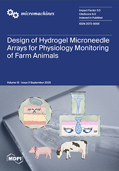
Microneedle arrays (MNAs) offer a minimally invasive way to monitor animal responses to heat and osmotic stress, key in adapting to global warming. These devices access interstitial fluid (ISF), which reflects blood biomarkers. While effective in humans, adapting MNAs for large farm animals like pigs and cattle requires redesign due to skin differences and species-specific behaviors. The study addressed these technological challenges to create effective MNAs with 37 microneedles, each 2.8 mm tall, using a biocompatible hydrogel (dextran-methacrylate). These arrays successfully pierced pig and cow skin and absorbed ~10 µL of fluid within 3 hours. This innovation supports improved physiological monitoring in livestock, addressing key challenges in animal health tracking under environmental stress. View this paper
  • Issues are regarded as officially published after their release is announced to the table of contents alert mailing list.
  • You may sign up for e-mail alerts to receive table of contents of newly released issues.
  • PDF is the official format for papers published in both, html and pdf forms. To view the papers in pdf format, click on the "PDF Full-text" link, and use the free Adobe Reader to open them.
Order results
Result details
Section
Select all
Export citation of selected articles as:
14 pages, 2128 KB  
Article
Safety Monitoring Method for Pipeline Crossing the Mining Area Based on Vibration–Strain Fusion Analysis
by Jianping He, Tongchun Qin, Zhe Zhang, Ronggui Liu and Yuping Bao
Micromachines 2025, 16(9), 1074; https://doi.org/10.3390/mi16091074 - 22 Sep 2025
Viewed by 120
Abstract
The overlying rock layers in a mining area may collapse or settle, subjecting pipelines to uneven forces that can lead to deformation or even fracture. This paper proposes a pipeline safety monitoring method that combines fiberoptic vibration and strain sensing to detect vibrations [...] Read more.
The overlying rock layers in a mining area may collapse or settle, subjecting pipelines to uneven forces that can lead to deformation or even fracture. This paper proposes a pipeline safety monitoring method that combines fiberoptic vibration and strain sensing to detect vibrations and deformations caused by rock layer collapse in mining zones. First, pipeline deformation monitoring under unknown force directions was investigated using fiber Bragg grating (FBG) sensing technology. Second, we constructed a mining area pipeline model and conducted vibration/deformation monitoring tests employing FBG sensors, distributed Brillouin strain sensing, and distributed fiberoptic vibration sensing technologies. The experimental results demonstrate that FBG sensor arrays deployed at 90-degree intervals can effectively identify the pipeline’s primary force direction and maximum strain, with direction angle errors of less than 5.2%. The integrated analysis of vibration and strain data enables accurate identification and measurement of extended vibration responses and pipeline deformations in open-air zones. This study establishes a comprehensive monitoring framework for ensuring pipeline safety in mining areas. Full article
(This article belongs to the Special Issue Fiber-Optic Technologies for Communication and Sensing)
Show Figures

Figure 1

22 pages, 9020 KB  
Article
Hybrid Inductively Coupled Plasma and Computer-Controlled Optical Surfacing Polishing for Rapid Fabrication of Damage-Free Ultra-Smooth Surfaces
by Wei Li, Peiqi Jiao, Dawei Luo, Qiang Xin, Bin Fan, Xiang Wu, Bo Gao and Qiang Chen
Micromachines 2025, 16(9), 1073; https://doi.org/10.3390/mi16091073 - 22 Sep 2025
Viewed by 124
Abstract
The polymer deposition layer (PDL) formed during inductively coupled plasma (ICP) processing significantly limits the figuring accuracy and surface quality of fused silica optics. This study investigates the formation mechanism, composition, and evolution of the PDL under varying dwell times and proposes an [...] Read more.
The polymer deposition layer (PDL) formed during inductively coupled plasma (ICP) processing significantly limits the figuring accuracy and surface quality of fused silica optics. This study investigates the formation mechanism, composition, and evolution of the PDL under varying dwell times and proposes an innovative dwell time gradient strategy to suppress roughness deterioration. A significant disparity in hardness and elastic modulus between the deposition layer and the substrate is revealed, explaining its preferential removal and protective buffering effect in computer-controlled optical surfacing (CCOS). A hybrid ICP-CCOS polishing process was developed for processing a ϕ100 mm fused silica mirror. The results show that within 33 min, the surface graphic error RMS was significantly reduced from 58.006 nm to 12.111 nm, and within 90 min, the surface roughness was ultra-precisely reduced from Ra 1.719 nm to Ra 0.151 nm. The average processing efficiency was approximately 0.63 cm2/min. Critically, a damage-free, ultra-smooth surface without subsurface damage (SSD) was successfully achieved. This hybrid process enables the simultaneous optimization of figure accuracy and roughness, eliminating the need for iterative figuring cycles. It provides a novel theoretical framework for high-precision figuring and post-ICP polymer removal, advancing the efficient fabrication of high-performance optics. Full article
(This article belongs to the Special Issue Advanced Manufacturing Technology and Systems, 4th Edition)
Show Figures

Figure 1

14 pages, 3445 KB  
Article
Hybrid Actuation MEMS Micromirror with Decoupled Piezoelectric Fast Axis and Electromagnetic Slow Axis for Crosstalk Suppression
by Haoxiang Li, Jiapeng Hou, Zheng Gong, Huijun Yu, Yue Liu and Wenjiang Shen
Micromachines 2025, 16(9), 1072; https://doi.org/10.3390/mi16091072 - 22 Sep 2025
Viewed by 124
Abstract
Electromagnetic micro-electro-mechanical system (MEMS) micromirrors are widely used in optical scanning systems but often encounter mechanical crosstalk due to the use of shared drive coils. This phenomenon leads to parasitic motion along the slow axis during fast-axis operation, resulting in undesirable elliptical scanning [...] Read more.
Electromagnetic micro-electro-mechanical system (MEMS) micromirrors are widely used in optical scanning systems but often encounter mechanical crosstalk due to the use of shared drive coils. This phenomenon leads to parasitic motion along the slow axis during fast-axis operation, resulting in undesirable elliptical scanning patterns that degrade image quality. To tackle this issue, a hybrid actuation scheme is proposed in which a piezoelectric actuator drives the fast axis through an S-shaped spring structure, achieving a resonance frequency of 792 Hz, while the slow axis is independently driven by an electromagnetic actuator operating in quasi-static mode. Finite element simulations and experimental measurements validate that the proposed decoupled design significantly suppresses mechanical crosstalk. When the fast axis is driven to a 40° optical scan angle, the hybrid system reduces the parasitic slow-axis deflection (typically around 1.43°) to a negligible level, thereby producing a clean single-line scan. The piezoelectric fast axis exhibits a quality factor of Q = 110, while the electromagnetic slow axis achieves a linear 20° deflection at 20 Hz. This hybrid design facilitates a distortion-free field of view measuring 40° × 20° with uniform line spacing, presenting a straightforward and effective solution for high-precision scanning applications such as LiDAR (Light Detection and Ranging) and structured light projection. Full article
Show Figures

Figure 1

19 pages, 3556 KB  
Article
Investigation of Scribing Parameters’ Influence on the Tomography and Crack Initiation of OLED Display Panels for Circular Structures
by Huaye Kong, Xijing Zhu, Guohong Li and Yao Liu
Micromachines 2025, 16(9), 1071; https://doi.org/10.3390/mi16091071 - 22 Sep 2025
Viewed by 127
Abstract
This paper focuses on the scoring-wheel cutting process for circular structures of OLED display panels, conducting in-depth research through an experiment–analysis–optimization system. Based on the Taguchi experimental design, a three-factor, five-level experiment is conducted, with the blade wheel angle (A), cutting speed (B), [...] Read more.
This paper focuses on the scoring-wheel cutting process for circular structures of OLED display panels, conducting in-depth research through an experiment–analysis–optimization system. Based on the Taguchi experimental design, a three-factor, five-level experiment is conducted, with the blade wheel angle (A), cutting speed (B), and pressure (C) set as influencing factors, and the scratch depth (h), width (w), median crack depth (l), and transverse crack width (d) set as evaluation indicators. The experiments are carried out using a self-developed dicing-wheel cutting device, and the morphology, roughness, and hardness of the cutting surface and cross-section are characterized by means of ultra-depth-of-field microscopy, laser confocal microscopy, microhardness tester, and other equipment. The research shows that the order of factors affecting the cutting quality is as follows: A > C > B. Through the analysis of morphology and crack characteristics, it is determined that the optimal parameter combination is a dicing wheel angle of 130°, a cutting speed of 20 mm/s, and a pressure of 11 N. The verification results indicate that this combination can reduce surface roughness, stabilize hardness, and realize efficient and precise processing of special-shaped structures in OLED display panels, providing strong theoretical and technical support for industrial process optimization. Full article
(This article belongs to the Special Issue Recent Advances in Micro/Nanofabrication, 2nd Edition)
Show Figures

Figure 1

11 pages, 4759 KB  
Article
A Study on the Transient Process of Contact-Mode Triboelectric Nanogenerators
by Shengyao Zhang, Hongchun Luo, Ru Zhang, Shun Ye, Haoyu Wei, Zhiqiang Zeng, Futi Liu and Guiyu Zhou
Micromachines 2025, 16(9), 1070; https://doi.org/10.3390/mi16091070 - 22 Sep 2025
Viewed by 169
Abstract
In the research of triboelectric nanogenerators (TENGs), most attention has been paid to material modification, structural design, and power management. Little study has been performed on the transient process of TENGs, although the capacitance characteristics of TENGs are well known. In this work, [...] Read more.
In the research of triboelectric nanogenerators (TENGs), most attention has been paid to material modification, structural design, and power management. Little study has been performed on the transient process of TENGs, although the capacitance characteristics of TENGs are well known. In this work, the transient process of contact-mode TENGs was studied by the infinite-plate model and verified by experimental tests. The results showed that TENGs exhibited a much higher output in the transient process than that in the steady state. Within the transient process, the transfer charge gradually grew to a maximum value, while the output current and power decreased. A formula to calculate the duration of the transient process was derived by Fourier expansion. This work also demonstrated an interesting transformation process of the Q-V curve in the transient process. Furthermore, the transient phenomenon was verified clearly in a contact-mode TENG sample fabricated by copper and polytetrafluoroethylene (PTFE) films through experimental tests. These results are useful for performance optimization of TENGs in applications. Full article
(This article belongs to the Special Issue Self-Tuning and Self-Powered Energy Harvesting Devices)
Show Figures

Figure 1

14 pages, 3624 KB  
Article
Design and Research of Superimposed Force Sensor
by Genshang Wu, Jinggan Shao, Yicun Xu, Zhanshu He and Shifei Liu
Micromachines 2025, 16(9), 1069; https://doi.org/10.3390/mi16091069 - 22 Sep 2025
Viewed by 156
Abstract
The measurement accuracy and equipment stability of superposition-type force sensors are primarily influenced by the layout and number of individual force sensors. Analyzing this impact effect through experimental testing for each configuration would consume significant manpower, material resources, and financial costs. To efficiently [...] Read more.
The measurement accuracy and equipment stability of superposition-type force sensors are primarily influenced by the layout and number of individual force sensors. Analyzing this impact effect through experimental testing for each configuration would consume significant manpower, material resources, and financial costs. To efficiently analyze the influence of the number of paralleled individual sensors and their layout within a superposition-type force measurement instrument on overall device stability and force measurement accuracy, this paper employs SolidWorks to establish models of force instruments based on common superposition schemes. Subsequently, ANSYS is utilized to perform finite element analysis on models of different schemes, obtaining corresponding data on total deformation, stress, and simulated force values. The analysis results indicate that a relatively sparse sensor layout with symmetric arrangement around the center point of the base plate enhances overall stability, and the force measurement error can be controlled within several ten-thousandths. Furthermore, the more stable and higher-accuracy schemes identified through simulation analysis were compared with practical experimental results to analyze theoretical versus actual errors. The test results showed that when the three single force sensors are placed in a “Pin font” shape, the sum of the forces measured by each individual sensor differs from the sum of the forces measured by the superimposed sensors by only a few ten-thousandths, which is within the acceptable range. Full article
(This article belongs to the Section E:Engineering and Technology)
Show Figures

Figure 1

16 pages, 5289 KB  
Article
Non-Invasive Three-Dimensional Cell Manipulation Technology Based on Acoustic Microfluidic Chips
by Lin Lin, Yiming Zhen, Wang Li, Guoqiang Dong, Rongxing Zhu and Minhui Liang
Micromachines 2025, 16(9), 1068; https://doi.org/10.3390/mi16091068 - 22 Sep 2025
Viewed by 234
Abstract
This study presents a non-invasive three-dimensional cell manipulation technique based on acoustic microfluidic chips, which generates acoustic flow fields through the vibration of micropillars induced by bulk acoustic waves to achieve precise multi-dimensional rotational manipulation of cells. Moreover, the characteristics of the acoustic [...] Read more.
This study presents a non-invasive three-dimensional cell manipulation technique based on acoustic microfluidic chips, which generates acoustic flow fields through the vibration of micropillars induced by bulk acoustic waves to achieve precise multi-dimensional rotational manipulation of cells. Moreover, the characteristics of the acoustic flow field under linear, quasi-circular, elliptical, and higher-order vibration modes were intensively studied, and the rotational manipulation performance of polystyrene microbeads and cancer cells was optimized by adjusting the frequency and voltage. The results showed that the rotational speed and direction of the particles varied significantly in different vibration modes, with the particles and cells achieving the highest rotational speed in the elliptical vibration mode (frequency: 44.9 kHz, and voltage: 60 Vpp). In addition, the technique successfully achieved in-plane and out-of-plane rotation of cancer cells, and cell viability tests showed that 94% of the cells remained active after manipulation, demonstrating the low damage and biocompatibility of the method. This study provides a new, efficient, precise and gentle approach to three-dimensional manipulation of cells, which holds significant potential in biomedical research and clinical applications. Full article
(This article belongs to the Special Issue Emerging Devices and Technologies in BioMEMS for Biomarker Detection)
Show Figures

Figure 1

9 pages, 2176 KB  
Article
High Power Density X-Band GaN-on-Si HEMTs with 10.2 W/mm Used by Low Parasitic Gold-Free Ohmic Contact
by Jiale Du, Hao Lu, Bin Hou, Ling Yang, Meng Zhang, Mei Wu, Kaiwen Chen, Tianqi Pan, Yifan Chen, Hailin Liu, Qingyuan Chang, Xiaohua Ma and Yue Hao
Micromachines 2025, 16(9), 1067; https://doi.org/10.3390/mi16091067 - 22 Sep 2025
Viewed by 186
Abstract
To enhance the RF power properties of CMOS-compatible gold-free GaN devices, this work introduces a kind of GaN-on-Si HEMT with a low parasitic regrown ohmic contact technology. Attributed to the highly doped n+ InGaN regrown layer and smooth morphology of gold-free ohmic [...] Read more.
To enhance the RF power properties of CMOS-compatible gold-free GaN devices, this work introduces a kind of GaN-on-Si HEMT with a low parasitic regrown ohmic contact technology. Attributed to the highly doped n+ InGaN regrown layer and smooth morphology of gold-free ohmic stacks, the lowest ohmic contact resistance (Rc) was presented as 0.072 Ω·mm. More importantly, low RF loss and low total dislocation density (TDD) of the Si-based GaN epitaxy were achieved by a designed two-step-graded (TSG) transition structure for the use of scaling-down devices in high-frequency applications. Finally, the fabricated GaN HEMTs on the Si substrate presented a maximum drain current (Idrain) of 1206 mA/mm, a peak transconductance (Gm) of 391 mS/mm, and a breakdown voltage (VBR) of 169 V. The outstanding material and DC performances strongly encourage a maximum output power density (Pout) of 10.2 W/mm at 8 GHz and drain voltage (Vdrain) of 50 V in active pulse mode, which, to our best knowledge, updates the highest power level for gold-free GaN devices on Si substrates. The power results reflect the reliable potential of low parasitic regrown ohmic contact technology for future large-scale CMOS-integrated circuits in RF applications. Full article
(This article belongs to the Section D:Materials and Processing)
Show Figures

Figure 1

11 pages, 2198 KB  
Article
Effect of Hafnium-Based Thin Film Thickness on Microstructure and Electrical of Yttrium-Doped Hafnium Oxide Ferroelectric Devices Prepared by Magnetron Sputtering
by Bei Ma, Ke Ma, Xinhui Qin, Yingxue Xi, Jin Zhang, Xinyu Yang, Pengfei Yang and Weiguo Liu
Micromachines 2025, 16(9), 1066; https://doi.org/10.3390/mi16091066 - 21 Sep 2025
Viewed by 187
Abstract
This study employs reactive magnetron sputtering technology to fabricate TiN/Y-HfO2/TiN multilayer thin film devices using titanium targets and yttrium-doped high-purity hafnium targets. A systematic investigation was conducted to explore the influence of hafnium-based thin film thickness on the structural and electrical [...] Read more.
This study employs reactive magnetron sputtering technology to fabricate TiN/Y-HfO2/TiN multilayer thin film devices using titanium targets and yttrium-doped high-purity hafnium targets. A systematic investigation was conducted to explore the influence of hafnium-based thin film thickness on the structural and electrical properties of TiN/Y-HfO2/TiN thin film devices. Radio frequency magnetron sputtering was utilized to deposit Y-HfO2 films of varying thicknesses on TiN electrodes by controlling deposition time, with a yttrium doping concentration of 8.24 mol.%. The surface morphology and crystal structure of the thin films were characterized using atomic force microscopy (AFM), Raman spectroscopy, X-ray diffraction (XRD). Results indicate that as film thickness increases, surface roughness and Raman peak intensity increase correspondingly, with the tetragonal phase (t) characteristic peak being most prominent at 65 nm. DC magnetron sputtering was employed to deposit TiN top electrodes, resulting in TiN/Y-HfO2/TiN thin film devices. Following rapid thermal annealing at 700 °C, electrical properties were evaluated using a ferroelectric tester. Leakage current density exhibited a decreasing trend with increasing film thickness, while the maximum polarization intensity gradually increased, reaching a maximum of 11.5 μC/cm2 at 120 nm. Full article
(This article belongs to the Special Issue Recent Advances in Thin-Film Devices)
Show Figures

Figure 1

18 pages, 4236 KB  
Article
End Surface Grinding Machinability of Zirconia Ceramics via Longitudinal–Torsional Coupled Vibration Rotary Ultrasonic Machining
by Fan Chen, Wenbo Bie, Kuohu Li and Xiaosan Ma
Micromachines 2025, 16(9), 1065; https://doi.org/10.3390/mi16091065 - 21 Sep 2025
Viewed by 232
Abstract
Zirconia (ZrO2) ceramics are advanced structural materials that exhibit exceptional performance in aerospace and other heavy-duty applications. Since conventional machining of ZrO2 ceramics presents significant challenges, this study employs the longitudinal–torsional coupled rotary ultrasonic machining (LTC-RUM) method for end surface [...] Read more.
Zirconia (ZrO2) ceramics are advanced structural materials that exhibit exceptional performance in aerospace and other heavy-duty applications. Since conventional machining of ZrO2 ceramics presents significant challenges, this study employs the longitudinal–torsional coupled rotary ultrasonic machining (LTC-RUM) method for end surface grinding of ZrO2 ceramics. To elucidate the material removal mechanism of LTC-RUM, an analysis was conducted from the perspective of individual abrasive grains. Subsequently, LTC-RUM experiments were carried out on ZrO2 ceramic samples to investigate the effects of processing parameters on cutting force, surface roughness, and surface morphology. The results show that cutting force decreases with lower spindle speed and ultrasonic power, but increases with higher feed rate and cutting depth. The surface roughness decreases with increasing spindle speed, yet increases with feed rate. Moreover, the surface roughness initially decreases and then increases with increasing ultrasonic power and cutting depth. Compared to conventional machining methods, LTC-RUM significantly reduces cutting force and surface roughness, thereby improving workpiece surface quality. This study provides valuable insights into the application of LTC-RUM for machining ZrO2 ceramics and other hard and brittle materials. Full article
Show Figures

Figure 1

13 pages, 1554 KB  
Article
Charge Trapping Effects on n−MOSFET Current Mirrors Under TID Radiation
by Dorsaf Aguir, Sedki Amor, Laurent A. Francis and Mohsen Machhout
Micromachines 2025, 16(9), 1064; https://doi.org/10.3390/mi16091064 - 20 Sep 2025
Viewed by 260
Abstract
This study aims to evaluate the effects of total ionizing dose (TID) radiation on the performance of n−MOSFET current mirrors. We propose an ovel experimental approach to analyze the interaction between charge trapping in the MOSFET gate oxide and the resulting current mirror degradation [...] Read more.
This study aims to evaluate the effects of total ionizing dose (TID) radiation on the performance of n−MOSFET current mirrors. We propose an ovel experimental approach to analyze the interaction between charge trapping in the MOSFET gate oxide and the resulting current mirror degradation by subjecting devices to TID doses from 50 krad(Si) to 300 krad(Si) using a 60Co gamma source Experimental data show that threshold voltage shifts by up to 1.31 V and transconductance increases by 27%. This degradation leads to this a reduction of more than 10% in current mirror output accuracy occurs at the highest dose. These quantitative criteria establish a clear benchmark for assessing the impact of TID on current mirror performance. These effects are attributed to positive charge trapping in the gate oxide and at the Si–SiO2 interface induced by ionizing radiation. This study focuses exclusively on radiation effects; electrical stress phenomena such as over−voltage or electrostatic discharge (ESD) are not addressed. The results highlight the critical importance of accounting for TID effects when designing high−performance n−MOSFET current mirrors for radiation−hardened applications. Full article
Show Figures

Figure 1

27 pages, 10722 KB  
Article
Improved Operation of the Modified Non-Inverting Step-Down/Up (MNI-SDU) DC-DC Converter
by Juan A. Villanueva-Loredo, Julio C. Rosas-Caro, Panfilo R. Martinez-Rodriguez, Christopher J. Rodriguez-Cortes, Diego Langarica-Cordoba and Gerardo Vazquez-Guzman
Micromachines 2025, 16(9), 1063; https://doi.org/10.3390/mi16091063 - 20 Sep 2025
Viewed by 154
Abstract
This paper presents an enhanced operation strategy for a recently proposed converter called Modified Non-Inverting Step-Down/Up (MNI-SDU) DC-DC converter intended for battery voltage regulation. Unlike the conventional approach, where both switching stages share a single duty cycle, the proposed method controls asynchronously the [...] Read more.
This paper presents an enhanced operation strategy for a recently proposed converter called Modified Non-Inverting Step-Down/Up (MNI-SDU) DC-DC converter intended for battery voltage regulation. Unlike the conventional approach, where both switching stages share a single duty cycle, the proposed method controls asynchronously the two duty cycles through a fixed time offset to optimize performance. A methodology is developed to define suitable duty cycle ranges that ensure proper converter operation according to input/output voltage specifications, while simultaneously reducing the current and voltage ripples and electrical stress in the capacitor and semiconductors. Furthermore, a model-based control strategy is proposed, taking into account the enhanced operational characteristics. Consequently, a PI-PI current-mode controller is designed using loop shaping techniques to maintain the output voltage regulated at the desired level. The proposed approach is analyzed mathematically and validated through experimental results. The findings demonstrate that optimizing through asynchronous duty-cycle control with a fixed time offset improves ripple, stress values, and overall efficiency, while maintaining robust output voltage regulation, making this method well-suited for applications requiring compact and reliable power conversion. Full article
(This article belongs to the Topic Power Electronics Converters, 2nd Edition)
Show Figures

Figure 1

14 pages, 2407 KB  
Article
LiDAR-Based Safety Envelope Detection with Accelerometer and DTW for Intrusion Localization in Roller Coasters
by Huajie Wang, Zhao Zhao, Yifeng Sun and Weikei Song
Micromachines 2025, 16(9), 1062; https://doi.org/10.3390/mi16091062 - 19 Sep 2025
Viewed by 226
Abstract
Autonomous vehicles, submersible robotic systems and drones, and other human-carrying equipment consistently adhere to a safety perimeter, ensuring collision-free navigation amidst surrounding objects. In contrast, roller coaster vehicles, despite being constrained to a predetermined track, necessitate frequent safety distance detection owing to the [...] Read more.
Autonomous vehicles, submersible robotic systems and drones, and other human-carrying equipment consistently adhere to a safety perimeter, ensuring collision-free navigation amidst surrounding objects. In contrast, roller coaster vehicles, despite being constrained to a predetermined track, necessitate frequent safety distance detection owing to the variability introduced by trees and decorative installations. Passengers’ limbs may protrude beyond vehicle boundaries, posing a collision hazard. The motion range of limbs, influenced by vehicle-specific conditions, mismatches standardized safety volumes (cylindrical, cubic, and rectangular) designed for mobile entities. The roller coaster industry’s current practice involves a moving safety frame, which visually inspects for collisions to assess safety distances, which is cumbersome and prone to oversight in intricate settings. Therefore, this study introduces a novel safety envelope detector (SE-detector). It creates a customer-defined virtual safety envelope around the roller coaster vehicle and measures the safety distance based on LiDAR (Light Detection and Ranging) to detect the intrusions of obstacles. Meanwhile, this SE-detector also innovatively integrated an accelerometer to synchronously measure the acceleration of the vehicle. The measured acceleration will be aligned with simulated sequences by dynamic time warping (DTW) algorithms to pinpoint intrusion location. Additionally, a wide-angle camera is also deployed to enhance perception of the surrounding environment. The SE-detector developed in this study has the capability to record inspection results. It is expected to enhance the inspection capabilities of the safety envelope for roller coasters, thereby improving the efficiency of safety distance inspection. Full article
(This article belongs to the Special Issue Micro/Nano Optical Devices and Sensing Technology)
Show Figures

Figure 1

11 pages, 1231 KB  
Article
Polyurethane-Based Electronic Packaging: The Characterization of Natural Aging over a Decade
by Xiaoqin Wei, Han Li, Rui Zhou, Changcheng Xie and Honglong Ning
Micromachines 2025, 16(9), 1061; https://doi.org/10.3390/mi16091061 - 18 Sep 2025
Viewed by 241
Abstract
Electronic devices with polyurethane electronic packaging have been stored in Chinese tropical marine atmosphere environments for 10 years. The long-term natural aging mechanism was studied by comparing the appearance inspection, molecular structure, elemental content, and chemical functional groups of the surface and interior [...] Read more.
Electronic devices with polyurethane electronic packaging have been stored in Chinese tropical marine atmosphere environments for 10 years. The long-term natural aging mechanism was studied by comparing the appearance inspection, molecular structure, elemental content, and chemical functional groups of the surface and interior of polyurethane electronic potting. The results indicated that, despite evident chemical aging and physical changes in the encapsulant material, it continued to effectively protect the internal electronic devices, maintaining their performance within an acceptable range. The interior polyurethane potting of electronic devices was white, but the surface turned yellow with noticeable color change. On the surface, the content of tolylene diisocyanate was greatly decreased. The peak heights of the internal carbamate groups located at 1708 cm−1 and 1529 cm−1 were significantly higher than those at the surface. In addition, the internal C element content for the carbamate group at 289.5 eV was higher than that of the surface. It can be inferred that, under ambient temperature and trace oxygen conditions, the urethane groups on the polyurethane electronic potting surface undergo aging reactions. These groups slowly oxidize into the quinoid structure of the chromophore, causing the surface to turn yellow. Despite this discoloration, the potting still protects electronic devices. Therefore, polyurethane electronic potting is ideal for the long-term sealed storage of electronic devices. Full article
(This article belongs to the Special Issue Advanced Packaging for Microsystem Applications, 3rd Edition)
Show Figures

Figure 1

10 pages, 3736 KB  
Article
A Reconfigurable Low-Pass Filter Based on Polyurethane Substrate Inspired by the Origami Structure
by Kang Wang, Mingcheng Li, Chuyuan Gao, Yupeng Dong, Yutang Pan, Ming Qin, Meng Nie and Lei Han
Micromachines 2025, 16(9), 1060; https://doi.org/10.3390/mi16091060 - 18 Sep 2025
Viewed by 243
Abstract
In this paper, an innovative reconfigurable microstrip RF device design method is proposed, which is inspired by origami structures. The experimental results of the reconfigurable low-pass filter indicate that the maximum origami folding height is 3 mm, resulting in the frequency tuning range [...] Read more.
In this paper, an innovative reconfigurable microstrip RF device design method is proposed, which is inspired by origami structures. The experimental results of the reconfigurable low-pass filter indicate that the maximum origami folding height is 3 mm, resulting in the frequency tuning range of the filter being 524~568 MHz, the return loss is below −15.0 dB and the insertion loss is below 2.5 dB up to 500 MHz. It is demonstrated that the proposed design method for reconfigurable microstrip RF devices is fairly effective through theoretical and experimental research. This work provides a groundbreaking method for reconfigurable RF devices with origami structures. Full article
Show Figures

Figure 1

13 pages, 10178 KB  
Article
Non-Free Cutting Mechanism of Asymmetrical Nanogrooves Under Chip-Removal Interference in Amorphous Nickel Phosphorus
by Yupeng He, Yingzhao Cai, Minkun Huang, Benshuai Ruan, Peng Liu and Tianfeng Zhou
Micromachines 2025, 16(9), 1059; https://doi.org/10.3390/mi16091059 - 18 Sep 2025
Viewed by 195
Abstract
Asymmetrical nanogrooves are commonly employed as blazed gratings for precision measurement, optical communication, and optical sensing applications. Diamond cutting is a promising deterministic processing technology for nanogrooves with a triangular cross-section profile. Non-free cutting of nanogrooves makes it hard to suppress the cutting-caused [...] Read more.
Asymmetrical nanogrooves are commonly employed as blazed gratings for precision measurement, optical communication, and optical sensing applications. Diamond cutting is a promising deterministic processing technology for nanogrooves with a triangular cross-section profile. Non-free cutting of nanogrooves makes it hard to suppress the cutting-caused deformation because of the low stiffness of nanogrooves. Focusing on the influence of non-free cutting on the deformation of asymmetrical nanogrooves, this paper systematically investigates the asymmetrical nanogroove cutting in amorphous nickel phosphorous material through mechanism revelation, simulation analysis, and experimental discussion. The materials removal mechanism by two side edges with different slopes in the non-free cutting is revealed according to the shear interference. According to the relative feed direction between tool and workpiece, two types of feed cases in the asymmetrical nanogrooves, named D1 and D2, respectively, are investigated by comparison in terms of deformation mechanism, nanogrooves topography, and nodal stress of tool edges. The extrusion by tool edges and the squeeze by the chip flow mainly influence the deformation of nanogrooves. In the D1 case, the horizontal component of squeeze by the chip flow towards the rear just-fabricated nanogroove, and the severely deformed nanogrooves are stacking together. On the contrary, in the D2 case, the flowing chip squeezes the front uncut materials, relieving the cutting-caused deformation, and asymmetrical nanogrooves have clear V-shaped cross-section profiles. It is proven that the D2 strategy is more suitable for asymmetrical nanogroove machining. The work in this paper will contribute to further understanding of non-free cutting and the processing technology of asymmetrical nanogrooves. Full article
(This article belongs to the Special Issue Ultra-Precision Micro Cutting and Micro Polishing)
Show Figures

Figure 1

23 pages, 8269 KB  
Article
A Novel Double-Diamond Microreactor Design for Enhanced Mixing and Nanomaterial Synthesis
by Qian Peng, Guangzu Wang, Chao Sheng, Haonan Wang, Yao Fu and Shenghong Huang
Micromachines 2025, 16(9), 1058; https://doi.org/10.3390/mi16091058 - 18 Sep 2025
Viewed by 311
Abstract
This study introduces the Double-Diamond Reactor (DDR), a novel planar passive microreactor designed to overcome the following conventional limitations: inefficient mass transfer, high flow resistance, and clogging. The DDR integrates splitting–turning–impinging (STI) hydrodynamic principles via CFD-guided optimization, generating chaotic advection to enhance mixing. [...] Read more.
This study introduces the Double-Diamond Reactor (DDR), a novel planar passive microreactor designed to overcome the following conventional limitations: inefficient mass transfer, high flow resistance, and clogging. The DDR integrates splitting–turning–impinging (STI) hydrodynamic principles via CFD-guided optimization, generating chaotic advection to enhance mixing. Experimental evaluations using Villermaux–Dushman tests showed a segregation index (Xs) as low as 0.027 at 100 mL·min−1, indicating near-perfect mixing. In BaSO4 nanoparticle synthesis, the DDR achieved a 46% smaller average particle size (95 nm) and narrower distribution (σg=1.27) compared to reference designs (AFR-1), while maintaining low pressure drops (<20 kPa at 60 mL·min−1). The DDR’s superior performance stems from its hierarchical flow division and concave-induced vortices, which eliminate stagnant zones. This work demonstrates the DDR’s potential for high-throughput nanomaterial synthesis with precise control over particle characteristics, offering a scalable and energy-efficient solution for advanced chemical processes. Full article
(This article belongs to the Section E:Engineering and Technology)
Show Figures

Figure 1

18 pages, 3172 KB  
Article
Enhancing Confidence and Interpretability of a CNN-Based Wafer Defect Classification Model Using Temperature Scaling and LIME
by Jieun Lee, Yeonwoo Ju, Junho Lim, Sungmin Hong, Soo-Whang Baek and Jonghwan Lee
Micromachines 2025, 16(9), 1057; https://doi.org/10.3390/mi16091057 - 17 Sep 2025
Viewed by 360
Abstract
Accurate classification of defects in the semiconductor manufacturing process is critical for improving yield and ensuring quality. While previous works have mainly focused on improving classification accuracy, we propose a model that can simultaneously assess accuracy, prediction confidence, and interpretability in wafer defect [...] Read more.
Accurate classification of defects in the semiconductor manufacturing process is critical for improving yield and ensuring quality. While previous works have mainly focused on improving classification accuracy, we propose a model that can simultaneously assess accuracy, prediction confidence, and interpretability in wafer defect classification. To solve the class imbalance problem, we used a weighted cross-entropy loss function and convolutional neural network–based model to achieve a high accuracy of 97.8% on the test dataset and applied a temperature-scaling technique to enhance confidence. Furthermore, by simultaneously employing local interpretable model-agnostic explanations and gradient-weighted class activation mapping, the rationale for the predictions of the model was visualized, allowing users to understand the decision-making process of the model from various perspectives. This research can provide a direction for the next generation of intelligent quality management systems by enhancing the applicability of the proposed model in actual semiconductor production sites through explainable predictions. Full article
(This article belongs to the Special Issue Semiconductor and Energy Materials and Processing Technology)
Show Figures

Figure 1

13 pages, 3296 KB  
Article
A 90–100 GHz SiGe BiCMOS 6-Bit Digital Phase Shifter with a Coupler-Based 180° Unit for Phased Arrays
by Hongchang Shen, Hongyun Zhang, Yuqian Pu, Chong Wang, Bing Li, Xusheng Tang, Xinxi Zeng and Jiang Luo
Micromachines 2025, 16(9), 1056; https://doi.org/10.3390/mi16091056 - 16 Sep 2025
Viewed by 362
Abstract
This paper presents a 90–100 GHz wideband digital phase shifter with a fine resolution of 5.625°, implemented in a 0.13 μm SiGe BiCMOS process. A switch-type architecture with six cascaded units, including a novel 180° cell based on a broadband coupler, enables full [...] Read more.
This paper presents a 90–100 GHz wideband digital phase shifter with a fine resolution of 5.625°, implemented in a 0.13 μm SiGe BiCMOS process. A switch-type architecture with six cascaded units, including a novel 180° cell based on a broadband coupler, enables full 0–360° phase coverage while improving phase accuracy, bandwidth, and process robustness. Post-layout simulations demonstrate an insertion loss below 15.5 dB, an RMS phase error under 2.3°, and an RMS amplitude error better than 0.9 dB across the 90–100 GHz band. The total chip area, including test pads, is 0.39 mm2, making the design compact and well suited for high-density phased-array applications. Full article
(This article belongs to the Section E:Engineering and Technology)
Show Figures

Figure 1

10 pages, 1726 KB  
Tutorial
Power-Law Reliability Plotting for Microelectronics
by Joseph B. Bernstein
Micromachines 2025, 16(9), 1055; https://doi.org/10.3390/mi16091055 - 16 Sep 2025
Viewed by 351
Abstract
The power-law time plotting for reliability prediction needs to be reexamined. Until now, most degradation plots in microelectronics reliability analysis assume that the data follow a power-law change in time. The plot is the change in a measured parameter versus the log of [...] Read more.
The power-law time plotting for reliability prediction needs to be reexamined. Until now, most degradation plots in microelectronics reliability analysis assume that the data follow a power-law change in time. The plot is the change in a measured parameter versus the log of time, based on the principle that one can calculate exactly the initial indicator value, S0, and from that, extrapolate any change in that parameter, ΔS(t), as a power-law with time, t1/m. The normalized change, ΔS(t)/S0, relies heavily on a precise value for S0 such that the calculated power-law exponent, m, may be exaggerated such that extrapolated time-to-fail calculations will be optimistic, even by many orders of magnitude. Also, the extrapolated lifetime may be pessimistic, also by orders of magnitude in time. We show that by transforming the x-axis as the time to a power of 1/m, choosing m by setting the second order of a polynomial curve fit to zero, a more accurate prediction can be achieved with a realistic time to fail given the accelerated testing conditions. We also show how to determine what the correct power of time is using a linear fit to a second-order polynomial. The plotting principles presented here are independent of any physics, rather an empirical focus on how to plot the data according to a power-law in time assumption. Full article
Show Figures

Figure 1

16 pages, 5065 KB  
Article
Surface Integrity of Glass-Ceramics by Laser-Assisted Diamond Cutting
by Jiawei Li, Fang Ji and Feifei Xu
Micromachines 2025, 16(9), 1054; https://doi.org/10.3390/mi16091054 - 16 Sep 2025
Viewed by 262
Abstract
Glass-ceramic optical components are extensively employed in advanced optical systems. The high-hardness and low-fracture toughness of glass-ceramics make it prone to cracks and subsurface damage during conventional cutting. The laser-assisted diamond cutting method can significantly improve the nano-cutting performance of glass-ceramics by locally [...] Read more.
Glass-ceramic optical components are extensively employed in advanced optical systems. The high-hardness and low-fracture toughness of glass-ceramics make it prone to cracks and subsurface damage during conventional cutting. The laser-assisted diamond cutting method can significantly improve the nano-cutting performance of glass-ceramics by locally heating and softening the material. However, its dynamic removal mechanisms remain unclear. The coupling mechanisms between the laser thermal field and the mechanical response of the material require further investigation. This study aims to reveal the dynamic removal mechanisms of glass-ceramics under laser-assisted nanoscale cutting conditions through numerical simulations and systematic experiments. It includes a systematic analysis of the effects of laser heating on chip morphology, temperature fields, stress fields, and cutting forces using a laser-assisted nano-cutting model. Additionally, through nanoscale taper cutting experiments, this study quantifies the enhancement effect of laser power on the critical depth of no observed surface cracks (NOSC). Finally, subsurface integrity results elucidate the mechanisms through which laser assistance inhibits crack propagation. The findings will provide theoretical support for optimizing laser-assisted cutting parameters and achieving high-quality machining of glass-ceramics. Full article
(This article belongs to the Special Issue Future Trends in Ultra-Precision Machining)
Show Figures

Figure 1

15 pages, 4560 KB  
Article
Harmonic-Recycling Passive RF Energy Harvester with Integrated Power Management
by Ruijiao Li, Yuquan Hu, Hui Li, Haiyan Jin and Dan Liao
Micromachines 2025, 16(9), 1053; https://doi.org/10.3390/mi16091053 - 15 Sep 2025
Viewed by 341
Abstract
The rapid growth of low-power Internet of Things (IoT) applications has created an urgent demand for compact, battery-free power solutions. However, most existing RF energy harvesters rely on active rectifiers, multi-phase topologies, or complex tuning networks, which increase circuit complexity and static power [...] Read more.
The rapid growth of low-power Internet of Things (IoT) applications has created an urgent demand for compact, battery-free power solutions. However, most existing RF energy harvesters rely on active rectifiers, multi-phase topologies, or complex tuning networks, which increase circuit complexity and static power overhead while struggling to maintain high efficiency under microwatt-level inputs. To address this challenge, this work proposes a harmonic-recycling, passive, RF-energy-harvesting system with integrated power management (HR-P-RFEH). The system adopts a planar microstrip architecture compatible with MEMS fabrication, integrating a dual-stage voltage multiplier rectifier (VMR) and a stub-based harmonic suppression–recycling network. The design was verified through combined electromagnetic/circuit co-simulations, PCB prototyping, and experimental measurements. Operating at 915 MHz under a 0 dBm input and a 2 kΩ load, the HR-P-RFEH achieves a stable 1.4 V DC output and a peak rectification efficiency of 70.7%. Compared with a conventional single-stage rectifier, it improves the output voltage by 22.5% and the efficiency by 16.4%. The rectified power is further regulated by a BQ25570-based unit to provide a stable 3.3 V supply buffered by a 47 mF supercapacitor, ensuring continuous operation under intermittent RF input. In comparison with the state of the art, the proposed fully passive, harmonic-recycling design achieves competitive efficiency without active bias or adaptive tuning while remaining MEMS- and LTCC-ready. These results highlight HR-P-RFEH as a scalable and fabrication-friendly building block for next-generation energy-autonomous IoT and MEMS systems. Full article
(This article belongs to the Special Issue Micro-Energy Harvesting Technologies and Self-Powered Sensing Systems)
Show Figures

Figure 1

7 pages, 187 KB  
Editorial
Converging Architectures: Precision Biomanufacturing and Soft Robotics Rewiring Tissue Engineering
by Miriam Filippi
Micromachines 2025, 16(9), 1052; https://doi.org/10.3390/mi16091052 - 15 Sep 2025
Viewed by 274
Abstract
Biomedicine is moving from sculpting tissues to engineering systems [...] Full article
(This article belongs to the Section B2: Biofabrication and Tissue Engineering)
16 pages, 1847 KB  
Article
The Fluidic Shear Stress Loading Method Enables Mechanobiological Stimulation in an On-Chip Pump-Integrated Microphysiological System
by Jin Hong Yap, Satoshi Ishizaki, Hiroko Nakamura, Kenta Shinha and Hiroshi Kimura
Micromachines 2025, 16(9), 1051; https://doi.org/10.3390/mi16091051 - 15 Sep 2025
Viewed by 437
Abstract
Microphysiological systems (MPSs), such as organ-on-a-chip platforms, are promising alternatives to animal testing for drug development and physiological research. The BioStellar™ Plate is a commercial MPS platform featuring an open-top culture chamber design with on-chip stirrer pumps that circulate culture medium through six [...] Read more.
Microphysiological systems (MPSs), such as organ-on-a-chip platforms, are promising alternatives to animal testing for drug development and physiological research. The BioStellar™ Plate is a commercial MPS platform featuring an open-top culture chamber design with on-chip stirrer pumps that circulate culture medium through six independent, dual microchannel-connected chamber multiorgan units. Although this design enables a circular flow, the open-top culture chamber format prevents the application of fluidic shear stress, a force that cells experience in vivo, which affects their behavior and function. To address this, we developed two fluidic shear stress attachments for the BioStellar™ Plate. These attachment channel fluids provide controlled mechanical stimulation to cultured cells. The flow dynamics were simulated using COMSOL Multiphysics to estimate shear stress levels. The attachments were fabricated and validated through fluorescent bead tracking and biological assays. The FSSA-D is designed for flat-bottom standard cell cultures, while the FSSA-I is designed for epithelial monolayers, enabling the application of fluidic shear stress across the basal membrane. Experiments with intestinal epithelial cells (Caco-2) demonstrated that both attachments enhanced cell barrier function under a fluidic environment, as indicated by higher transepithelial electrical resistance (TEER). These findings demonstrate that the attachments are practical tools for mechanobiology research with MPS platforms. Full article
Show Figures

Figure 1

15 pages, 9265 KB  
Article
On-Machine Precision Truing and Error Compensation of Cup-Shaped Diamond Grinding Wheels with Arc-Shaped Cutting Edge
by Yawen Guo and Ziqiang Yin
Micromachines 2025, 16(9), 1050; https://doi.org/10.3390/mi16091050 - 15 Sep 2025
Viewed by 339
Abstract
The cup-shaped grinding wheels with arc-shaped edges provide a satisfactory precision grinding solution for high-accuracy optical surfaces on hard and brittle materials. However, the complex profile of the arc-shaped edges of cup-shaped grinding wheels makes them challenging to truing. This paper proposes an [...] Read more.
The cup-shaped grinding wheels with arc-shaped edges provide a satisfactory precision grinding solution for high-accuracy optical surfaces on hard and brittle materials. However, the complex profile of the arc-shaped edges of cup-shaped grinding wheels makes them challenging to truing. This paper proposes an on-machine truing technique targeting cup-shaped grinding wheels with arc-shaped cutting edge. First, a mathematical model was established to simulate the three-axis of on-machine truing the arc-shaped cutting edge using a diamond roller. Based on this model, a theoretical analysis is conducted to investigate the impact of tool setting errors, measurement errors of the diamond roller, and the pose error on truing accuracy. A compensation method was proposed, and experimental results validated its effectiveness. To investigate the grinding performance of cup-shaped grinding wheels after truing, a complex component is ground using a truing diamond grinding wheel. The experimental results demonstrate that this method enables precise on-machine truing of the arc-shaped edges of cup-shaped grinding wheels and is efficient. The average dimensional accuracy of the grinding wheel’s arc-shaped edge is reduced to 1.5 μm, with the profile accuracy (PV) of 0.89 μm. Full article
Show Figures

Figure 1

13 pages, 14630 KB  
Article
Atomic Insight into the Nano-Grinding Mechanism of Reaction-Bonded Silicon Carbide: Effect of Abrasive Size
by Honglei Mo, Xie Chen, Cui Luo and Xiaojiang Cai
Micromachines 2025, 16(9), 1049; https://doi.org/10.3390/mi16091049 - 15 Sep 2025
Viewed by 336
Abstract
Reaction-bonded silicon carbide (RB-SiC) is a high-performance ceramic material known for its excellent mechanical, thermal, and chemical properties. It contains phases with different mechanical properties, which introduce complex machining mechanisms. In the present work, molecular dynamics (MD) simulation was conducted to investigate the [...] Read more.
Reaction-bonded silicon carbide (RB-SiC) is a high-performance ceramic material known for its excellent mechanical, thermal, and chemical properties. It contains phases with different mechanical properties, which introduce complex machining mechanisms. In the present work, molecular dynamics (MD) simulation was conducted to investigate the effect of abrasive size on the nano-grinding mechanism of RB-SiC. The surface morphology and subsurface deformation mechanism were investigated. The simulation results suggest that when a small abrasive is used, the surface swelling of SiC is primarily generated by the bending and tearing of SiC at the interfaces. As the abrasive radius increases, the surface swelling is mainly formed by Si atoms, which is identified as elastic recovery. Meanwhile, the material removal rate gradually decreases, and the depth of plastic deformation is obviously increased. Stocking of Si is more apparent at the interface, and obvious sliding of SiC grains is observed, forming edge cracks at the margin of the workpiece. In the subsurface workpiece, the high-pressure phase transition (HPPT) of Si is promoted, and the squeeze of disordered Si is obvious with more dislocations formed when larger abrasive is used. Full article
(This article belongs to the Special Issue Future Trends in Ultra-Precision Machining)
Show Figures

Figure 1

11 pages, 2762 KB  
Article
Study on the Low-Damage Material Removal Mechanism of Silicon Carbide Ceramics Under Longitudinal–Torsional Ultrasonic Grinding Conditions
by Junli Liu, Zhenqi Ma, Yanyan Yan, Dengke Yuan and Yifan Wang
Micromachines 2025, 16(9), 1048; https://doi.org/10.3390/mi16091048 - 13 Sep 2025
Viewed by 439
Abstract
In order to achieve the high-performance machining of silicon carbide (SiC) ceramics, longitudinal–torsional ultrasonic vibration (LTUV) was introduced into precision machining, and a systematic investigation into the effects of various process parameters on the critical cutting depth and surface quality was conducted. This [...] Read more.
In order to achieve the high-performance machining of silicon carbide (SiC) ceramics, longitudinal–torsional ultrasonic vibration (LTUV) was introduced into precision machining, and a systematic investigation into the effects of various process parameters on the critical cutting depth and surface quality was conducted. This investigation was undertaken with a view to exploring the ultrasonic vibration-assisted grinding mechanism of SiC ceramics. Firstly, the kinematic model of single abrasive grain trajectory and the maximum unaltered cutting thickness during longitudinal–torsional ultrasonic vibration-assisted grinding (LTUVG) was established to explore its unique grinding characteristics. On this basis, the theoretical modeling of critical cutting depth in SiC ceramics under LTUVG conditions was developed. This was then verified through longitudinal–torsional ultrasonic scratching (LTUS) experiments, and the theoretical analysis and test results prove that compared with normal scratching, the quality of SiC grooves are significantly improved by means of LTUS. During LTUS experiments, the dynamic fracture toughness, strain rate of SiC, and high-frequency ultrasonic excitation significantly enhances SiC performance, increasing the critical cutting depth and expanding the plastic removal region, so it is easy for LTUVG to yield the better surface quality in machined SiC ceramics, which provides important scholarly support for achieving the low-damage machining of SiC ceramics. Full article
Show Figures

Figure 1

38 pages, 8196 KB  
Review
Morph and Function: Exploring Origami-Inspired Structures in Versatile Robotics Systems
by Tran Vy Khanh Vo, Tan Kai Noel Quah, Li Ting Chua and King Ho Holden Li
Micromachines 2025, 16(9), 1047; https://doi.org/10.3390/mi16091047 - 13 Sep 2025
Viewed by 536
Abstract
The art of folding paper, named “origami”, has transformed from serving religious and cultural purposes to various educational and entertainment purposes in the modern world. Significantly, the fundamental folds and creases in origami, which enable the creation of 3D structures from a simple [...] Read more.
The art of folding paper, named “origami”, has transformed from serving religious and cultural purposes to various educational and entertainment purposes in the modern world. Significantly, the fundamental folds and creases in origami, which enable the creation of 3D structures from a simple flat sheet with unique crease patterns, serve as a great inspiration in engineering applications such as deployable mechanisms for space exploration, self-folding structures for exoskeletons and surgical procedures, micro-grippers, energy absorption, and programmable robotic morphologies. Therefore, this paper will provide a systematic review of the state-of-the-art origami-inspired structures that have been adopted and exploited in robotics design and operation, called origami-inspired robots (OIRs). The advantages of the flexibility and adaptability of these folding mechanisms enable robots to achieve agile mobility and shape-shifting capabilities that are suited to diverse tasks. Furthermore, the inherent compliance structure, meaning that stiffness can be tuned from rigid to soft with different folding states, allows these robots to perform versatile functions, ranging from soft interactions to robust manipulation and a high-DOF system. In addition, the potential to simplify the fabrication and assembly processes, together with its integration into a wide range of actuation systems, further broadens its capabilities. However, these mechanisms increase the complexity in theoretical analysis and modelling, as well as posing a challenge in control algorithms when the robot’s DOF and reconfigurations are significantly increased. By leveraging the principles of folding and integrating actuation and design strategies, these robots can adapt their shapes, stiffness, and functionality to meet the demands of diverse tasks and environments, offering significant advantages over traditional rigid robots. Full article
Show Figures

Figure 1

14 pages, 3393 KB  
Article
Optical Sensor for Scanning Angle of Micromirror with Improved 2D Calibration Method
by Longqi Ran, Zhongrui Ma, Ting Li, Jiangbo He, Jiahao Wu and Wu Zhou
Micromachines 2025, 16(9), 1046; https://doi.org/10.3390/mi16091046 - 13 Sep 2025
Viewed by 324
Abstract
The optical angle sensor demonstrates considerable potential to supersede the piezoresistive sensor as the preferred angle detection mechanism for micromirrors, primarily due to its reduced vulnerability to temperature fluctuations. However, this sensor is susceptible to interference from rotations about non-detectable axes and exhibits [...] Read more.
The optical angle sensor demonstrates considerable potential to supersede the piezoresistive sensor as the preferred angle detection mechanism for micromirrors, primarily due to its reduced vulnerability to temperature fluctuations. However, this sensor is susceptible to interference from rotations about non-detectable axes and exhibits inadequate linearity. To mitigate these challenges, this paper introduces a sub-region calibration method. A mapping surface was created to link the output signal offsets of two axes with their input angles, allowing the effects of non-measured axes to be treated as variables. To simplify the mathematical model of this mapping surface, it was divided into an n-by-n grid of small areas. Each area uses bilinear interpolation to calculate the corresponding angle from the output values. To quickly locate which grid area a sensor output belongs to, the entire mapping surface was scaled to a range from 0 to n. Sensor outputs are then assigned to specific grid areas using the floor function. For validation, an optical sensor and a 2D rotating stage were built for calibration tests. Experimental results show that this calibration method keeps measurement errors below 0.01° within a ±8° operating range of the sensor. Full article
(This article belongs to the Special Issue Recent Advances in MEMS Mirrors)
Show Figures

Figure 1

11 pages, 4467 KB  
Article
An Overmoded-Waveguide-Based Permittivity Measurement Method with High Accuracy and Ultra-Broadband over 8–110 GHz
by Weijie Wang, Yingjian Cao, Tieyang Wang, Fangfang Song, Shuanzhu Fang, Xianfeng Tang, Xiangqiang Li, Guoxiang Shu and Guo Liu
Micromachines 2025, 16(9), 1045; https://doi.org/10.3390/mi16091045 - 12 Sep 2025
Viewed by 433
Abstract
An overmoded-waveguide-based kit operating in 8–110 GHz for material complex permittivity measurement is proposed and designed in this paper. It overcomes the significant errors caused by air gaps in the conventional standard waveguide method (SWM), especially for millimeter-wave frequency bands. Furthermore, it avoids [...] Read more.
An overmoded-waveguide-based kit operating in 8–110 GHz for material complex permittivity measurement is proposed and designed in this paper. It overcomes the significant errors caused by air gaps in the conventional standard waveguide method (SWM), especially for millimeter-wave frequency bands. Furthermore, it avoids the problem of SWM requiring different samples in broadband measurements. The proposed kit consists of an overmoded-waveguide sample fixture with cross dimensions of 22.86 mm × 10.16 mm, seven pairs of standard-overmoded waveguide transition structures for different frequency bands, and thru-reflect-line calibration kits. The air gap problem, a major error source in millimeter-wave measurement, is quantitatively investigated. Compared with the SWM method, the proposed kit can decrease errors from over 68% to below 8%. The proposed method was verified by measuring the polytetrafluoroethylene sample. Then, it was applied to measure the BeO-TiO2 ceramic, which is widely used in vacuum devices. The measured data are valuable for applying BeO-TiO2 ceramics in relevant devices and developing its dielectric relaxation model. Full article
(This article belongs to the Special Issue Microwave Passive Components, 3rd Edition)
Show Figures

Figure 1

Previous Issue
Next Issue
Back to TopTop