


Abstract
In this paper, the design and simulation of a monolithically integrated silicon carbide (SiC) MEMS piezoresistive accelerometer with an on-chip SiC field-effect transistor (SiC-FET) readout circuit are presented for applications in harsh environments. The proposed device can be fully realized on a single SiC platform, ensuring robust operation at a very high temperature (1000 K) and removing the bottlenecks associated with heterogeneous integration and silicon-based sensor electronics. Finite-element-method (FEM) simulations were performed to investigate the mechanical performance of the accelerometer, including sensitivity, cross-axis response, resonant frequency, and thermal stability. The designed accelerometer exhibits a z-axis sensitivity of 35.8 /g with low cross-axis sensitivities of 0.27% and 2.12% along the x- and y-axes, respectively. The eigen frequency analysis shows a fundamental resonance frequency of 1640 Hz and an operating bandwidth of 328 Hz. Thermal simulations indicate excellent stability performance from 300 K to 1000 K with resistance and displacement variations of less than 0.21% and 0.009%, respectively. A 4H-SiC MOSFET was designed and analyzed by the TCAD process and device simulations. It was shown to operate stably in a wide temperature range without breakdown. The FEM and TCAD results were incorporated into a Verilog-A model and implemented in Cadence Virtuoso to evaluate the complete sensor-readout system. The integrated SiC-FET common-source amplifier achieved a sensitivity of up to 100 mV/V at 1000 K with a non-linearity of approximately 1%. The results demonstrate the feasibility of a fully integrated all-SiC accelerometer platform for high-temperature sensing applications in aerospace, automotive, energy, and industrial environments.
1. Introduction
Demand for reliable sensor systems in harsh environments, typically at very high temperatures, has increased significantly in recent years, driven by applications in aerospace propulsion, gas turbines, nuclear power plants, deep-well drilling, automotive engines, and industrial process monitoring [1,2,3]. In these environments, sensor systems are exposed to elevated temperatures, high vibration levels, corrosive media, and intense radiation. Among the various sensing devices, accelerometers play a critical role in structural health monitoring, vibration analysis, condition-based maintenance, and inertial navigation [4]. Reliability problems and performance degradations of conventional silicon (Si)-based microelectromechanical system (MEMS) accelerometers at elevated temperatures are still a challenge. Degradation is primarily caused by the increased intrinsic carrier concentration, leakage currents and the onset of irreversible plastic deformation at temperatures above ∼500 °C. These limitations restrict their utilization in next-generation high-temperature sensing systems [5,6].
Both SiC and GaN are promising wide-bandgap semiconductors and are explored for harsh-environment electronic and MEMS applications, high critical electric fields, and excellent thermal stability. However, SiC is preferred for MEMS sensing applications because of its superior thermal conductivity, higher Young’s modulus, excellent chemical stability, and well-established bulk micromachining technology [7,8]. These characteristics enable reliable operation under harsh environments and facilitate the monolithic integration of MEMS sensors with SiC-based electronics. Silicon carbide (SiC) has emerged as one of the most promising semiconductor materials for harsh-environment MEMS applications. SiC is a wide bandgap semiconductor with excellent material properties such as a high breakdown electric field, excellent thermal conductivity, superior mechanical strength, outstanding chemical inertness and excellent radiation tolerance [7]. Moreover the wide bandgap of 4H-SiC (∼3.2 eV) allows stable electrical operation at temperatures far above the range of silicon-based devices. The high Young’s modulus of SiC, around three times that of silicon, also provides better structural rigidity and mechanical reliability under extreme operating conditions. And the piezoresistive effect in SiC remains significant at high temperatures. SiC is a promising material for the fabrication of high-temperature MEMS sensors [7,8].
Extensive research has been conducted on SiC-based MEMS devices, particularly pressure sensors, where both all-SiC and bulk-SiC approaches have demonstrated excellent performance in harsh environments [9,10,11]. In contrast, the development of SiC MEMS accelerometers remains relatively limited. Many reported SiC accelerometers employ hybrid structures in which thin SiC films are deposited on silicon substrates to form the sensing layer while retaining silicon as the structural material [12,13]. Although such approaches exploit some advantages of SiC, the thermal limitations of the underlying silicon substrate prevent operation in truly extreme environments. To overcome this limitation, several researchers have investigated bulk-SiC and all-SiC accelerometers. Okojie et al. developed a bulk SiC piezoresistive accelerometer for high-temperature and high-shock applications, and later studies demonstrated all-SiC accelerometers that can operate in extreme acceleration environments [14]. However, such devices usually exhibit relatively low sensitivity or require complex fabrication processes including deep SiC etching, wafer thinning and multiple assembling steps [15].
Another significant challenge in existing SiC accelerometer technologies is the lack of monolithic integration between the sensing element and the signal-conditioning electronics [16]. Most reported devices rely on external silicon-based amplification and readout circuits, which become the limiting factor for high-temperature operation. Long interconnections between the sensor and external electronics also increase parasitic capacitance, electromagnetic interference susceptibility, and signal degradation [17]. Therefore, achieving monolithic integration of sensing and electronic functions on a single SiC platform is highly desirable for improving system reliability, reducing packaging complexity, minimizing parasitic effects, and enabling fully integrated harsh-environment sensing solutions [18].
The recent progress in SiC microfabrication and SiC electronic devices opens up new opportunities for monolithically integrated MEMS sensors. SiC field-effect transistors (FETs) have shown stable operation at high temperatures and can be used as on-chip signal-conditioning elements [19,20]. Integration of SiC piezoresistive sensing structures and SiC FET readout circuits on a single wafer provides several advantages including reduced interconnection losses, improved signal-to-noise ratio, compact device footprint, simplified packaging and compatibility with high-temperature operation. This single-wafer approach also paves the way towards fully integrated smart sensing systems that can operate in environments that are inaccessible to conventional silicon technologies.
However, while the benefits are significant, the research on co-design of SiC MEMS accelerometers and SiC FET readout circuits is still limited. A major design challenge is to simultaneously optimize mechanical sensitivity, piezoresistive transduction efficiency, transistor performance and electromechanical coupling [21,22]. Moreover, the effect of structural dimensions, stress distribution, proof mass geometry and FET biasing conditions on the overall sensor performance requires a systematic investigation.
In this work, design and simulation of a monolithically integrated SiC MEMS accelerometer with an on-chip SiC FET readout circuit are proposed and analyzed. The sensor and signal-conditioning electronics are realized on a single SiC wafer, eliminating the need for heterogeneous integration and enabling a compact all-SiC sensing platform suitable for harsh-environment applications. The accelerometer uses a piezoresistive transduction mechanism, where stress-induced resistance variations are directly converted into electrical signals and amplified by the SiC-FET-based common-source amplifier. The finite-element simulations are performed in COMSOL version 6.4 multiphysics to evaluate the mechanical behavior of the SiC-MEMS accelerometer structure, displacement characteristics, resonance frequency, and sensitivity for different accelerations at temperatures varying from 300 K to 1000 K. The SiC-FET process and device simulations are further conducted in TCAD to investigate the electrical performance of the SiC FET at varying temperatures. Both FEM and TCAD results are combined together and used to design a SiC-FET-MEMS-based common-source amplifier in Cadence. The proposed architecture demonstrates the feasibility of single-wafer monolithic integration of MEMS sensing structures and SiC electronics, providing a promising route toward next-generation high-temperature intelligent sensor systems.
2. SiC MEMS Accelerometer: FEM Design
2.1. Sensor Design
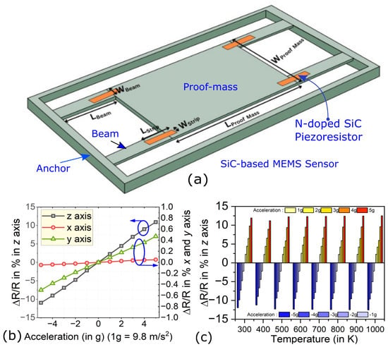
A SiC-based piezoresistive accelerometer can be modeled as a second-order dynamic system comprising a proof mass, suspension springs, and damping elements. A four-flexure SiC accelerometer is widely used [23] and is chosen for the present work. The proposed MEMS accelerometer consists of a central cuboidal proof mass supported by four suspension beams located at each corner, as shown in Figure 1a.
Figure 1.
(a) Proposed SiC MEMS accelerometer designed in COMSOL Multiphysics; (b) relative resistance change () as a function of applied acceleration along the z-, x-, and y-axes; (c) relative resistance change for applied accelerations from −5 g to +5 g at temperatures ranging from 300 K to 1000 K, where upper arrow shows acceleration varying from 1 g to 5 g, and lower arrow shows acceleration varying from −1 g to −5 g.
The proof mass has dimensions of 6000 μm × 5000 μm ×80 μm, providing sufficient inertial mass to respond effectively to external accelerations. Each suspension beam has dimensions of 1250 μm × 200 μm × 20 μm, ensuring adequate flexibility while maintaining structural integrity. The design parameters are shown in Table 1. Both the proof mass and suspension beams are fabricated from bulk silicon carbide (SiC), selected for its excellent mechanical strength, thermal stability, and suitability for harsh-environment applications.
Table 1.
Dimensions of the proposed SiC piezoresistive accelerometer.
To enable acceleration sensing, n-doped SiC piezoresistive elements with dimensions of 340 μm × 40 μm × 2 μm are deposited at the beam–proof mass junctions, where the mechanical stress is maximized. The resistance variation in these piezoresistors is monitored to determine the applied acceleration.
When a linear acceleration is applied, the proof mass experiences an inertial force, causing displacement relative to the supporting frame. The suspension beams behave as mechanical springs and generate a restoring force that opposes the displacement. The mechanical restoring force can be expressed using Hooke’s law as [21,24]
where is the restoring force, is the equivalent spring constant of the suspension system, and x is the displacement of the proof mass.
2.2. Device Sensitivity Analysis
The mechanical sensitivity of the accelerometer is defined as the change in piezoresistance per unit of applied acceleration and is expressed in /g, where 1 g = .
The sensor was primarily designed for acceleration measurements along the z-axis. Simulation results indicate a highly linear and sensitive response in this direction. Within of acceleration application, the piezoresistance varied from at g to at g, relative to a nominal resistance of approximately at zero acceleration. Consequently, the z-axis sensitivity was calculated as
In contrast, the x-axis exhibited only minor resistance variation, corresponding to a sensitivity of
Similarly, the y-axis resistance yielded a sensitivity of
The cross-axis sensitivity is defined as the ratio of the off-axis sensitivity to the primary-axis sensitivity and is given by
and
Substituting the calculated sensitivities yields cross-axis sensitivities of = 0.27% and = 2.12%. The low cross-axis sensitivity values demonstrate excellent directional selectivity and minimal interference from lateral accelerations.
In Figure 1b, the relative mechanical sensitivity or resistance variation in the accelerometer for −5 g to 5 g acceleration in the x,y and z directions is illustrated. It can be observed that the relative resistance variation ( g)) is about 12% in the z-axis, which reduces to less than 0.5% in the x- and 0.5% in the y-axis. However, percentage change in in the z-axis remains almost unchanged for the ±5 g acceleration range at operating temperatures ranging from 300 K to 1000 K, as depicted in Figure 1c.
2.3. Eigen Frequency Analysis
Eigen frequency analysis was performed to determine the natural frequencies and vibration modes of the proposed accelerometer. The first three resonant modes are summarized in Table 2.
Table 2.
Natural frequencies and corresponding vibration modes of the proposed SiC MEMS accelerometer.
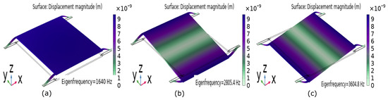
The first eigen frequency was obtained at 1640 Hz (Figure 2a) and corresponded to the desired translational motion of the proof mass along the z-axis. The second and third eigen frequencies occurred at 2805.4 Hz and 3604.8 Hz, respectively, representing rotational modes about the y-axis and x-axis (Figure 2b,c).
Figure 2.
Modal analysis of proposed SiC accelerometer, (a) Mode 1 in z axis, (b) mode 2 in y axis, (c) mode 3 in x axis.
According to the commonly accepted design criterion that MEMS accelerometers exhibit a flat frequency response up to approximately 20% of their first natural frequency, the usable operating bandwidth can be estimated as 328 Hz. Furthermore, the large separation between the first and second natural frequencies, , reduces the likelihood of unintended excitation of rotational modes due to environmental vibrations, thereby enhancing measurement stability.
2.4. Heat Transfer Analysis
Thermal analysis was performed in COMSOL Multiphysics using coupled electro-thermo-mechanical simulations. The analysis considered Joule heating arising from electrical biasing, thermally induced structural deformation, and temperature-dependent variations in piezoresistive characteristics.
A thermal sweep from 300 K to 1000 K was conducted to evaluate the suitability of the proposed accelerometer for harsh-environment applications. The simulation results demonstrated excellent thermal stability throughout the investigated temperature range, with negligible variations in both electrical and mechanical performance, which aligned with the trend of 4H-SiC electrical behavior at high temperatures [25,26]. For an applied acceleration of 2 g along the z-axis, the piezoresistance was at 300 K and at 1000 K. The corresponding percentage variation was . Similarly, the average displacement of the proof mass was nm at 300 K and nm at 1000 K. The percentage variation was calculated as .
These results indicate that the proposed SiC MEMS accelerometer maintains both electrical and mechanical stability over a wide temperature range, confirming its suitability for operation in harsh thermal environments.
3. Materials and Methods
3.1. Two-Dimensional TCAD Process Simulation of the 4H-SiC MOSFET
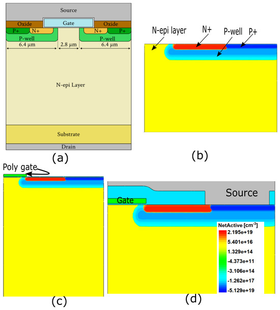
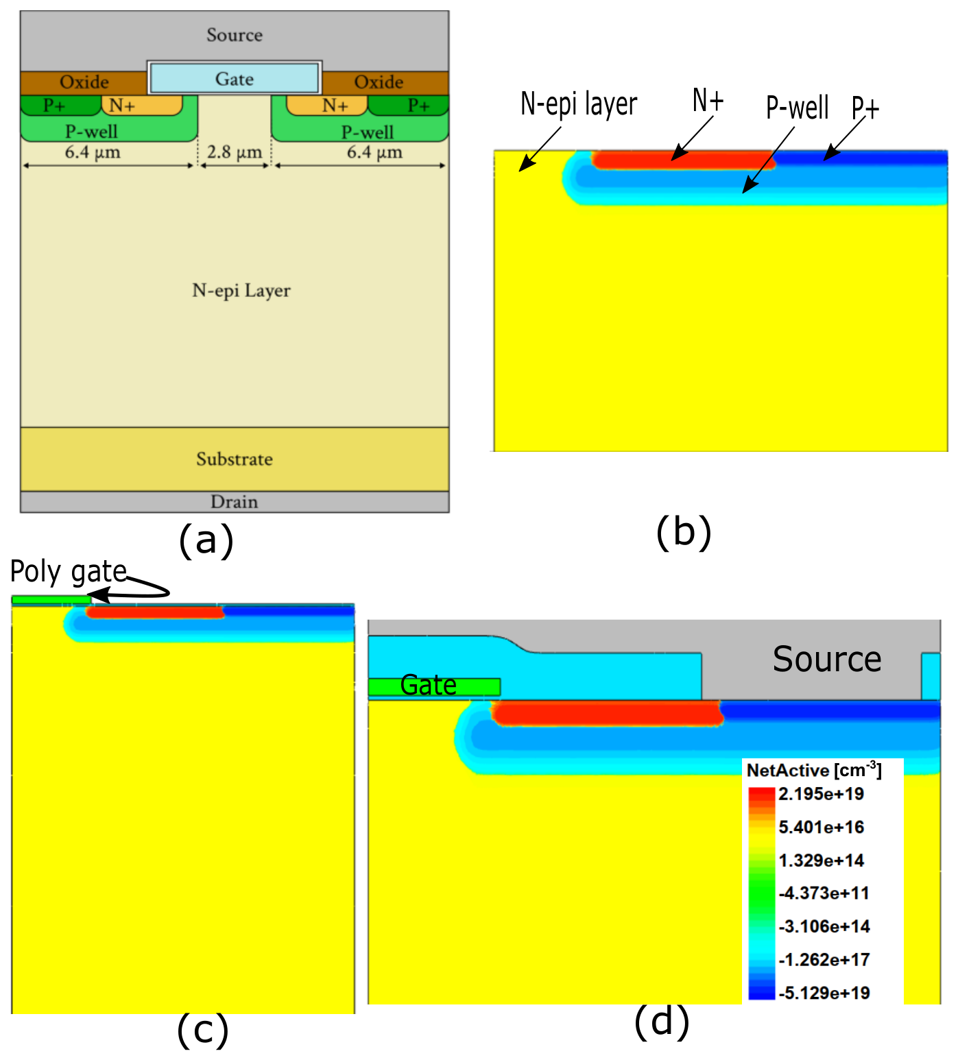
The two-dimensional process simulation of a vertical 4H-SiC power MOSFET was carried out with Synopsys Sentaurus SProcess TCAD tool (Version X-2025.06, Synopsys Inc., Irvine, CA, USA) [27] (Figure 3a). The simulation was based on the calibrated 4H-SiC process models including Monte Carlo ion implantation and high-temperature dopant activation models. The process flow was designed to replicate fabrication of a conventional vertical n-channel SiC MOSFET including an n-type drift layer, p-well region, heavily doped source/body contact regions, gate oxide, polysilicon gate and source metallization.
Figure 3.
(a) Designed SiC FET (not to scale). Process steps: (b) annealing after doping, (c) poly gate deposition and patterning, and (d) metallization for source contact formation.
The simulation domain was initialized with a 12 μm thick 4H-SiC substrate and nitrogen concentration of . The process sequence was simulated with adaptive meshing that was further refined at material interfaces and heavily doped regions to adequately resolve steep doping gradients and interface characteristics.
The voltage-blocking drift region was formed by growing a 12 μm thick n-type epitaxial layer on the SiC substrate. Nitrogen was employed as the donor dopant with a concentration of . To emulate epitaxial growth, the layer was deposited in three sequential steps followed by thermal diffusion at 1600 °C. This approach enabled realistic dopant incorporation and redistribution within the drift region.
The p-well region was formed through aluminum ion implantation using a lithographically defined mask. Multiple implantation energies were utilized to obtain a relatively uniform dopant profile and the desired junction depth. The implantation sequence consisted of 200, 300, 400, and 500 keV implantations with a cumulative dose of approximately . Local mesh refinement was applied around the implantation window to accurately resolve the implanted dopant distribution.
The n+ source region was formed using nitrogen implantation with a dose of at an implantation energy of 120 keV. Subsequently, a p+ body contact region was created using aluminum implantation with a dose of at 120 keV. These heavily doped regions reduce contact resistance and provide effective body contact operation.
Following implantation, high-temperature activation annealing was performed at 1800 °C for 5 min to activate the implanted dopants and repair implantation-induced crystal damage (Figure 3b).
A gate dielectric layer was formed by depositing a 50 nm thick SiO2 layer on the SiC surface. The oxide thickness was extracted during the simulation to verify process accuracy. Subsequently, a 0.2 μm thick polysilicon layer was deposited and patterned to form the gate electrode. Additional mesh refinement was introduced at the SiO2/4H-SiC interface to improve the accuracy of subsequent electrical simulations (Figure 3c).
An interlayer dielectric (ILD) consisting of silicon dioxide was deposited with a thickness of 0.5 μm. Contact openings were subsequently formed by anisotropic oxide etching. A 1 μm thick aluminum layer was then deposited to establish the source metallization (Figure 3d). While aluminum is used in the TCAD process simulation for demonstration purposes, practical high-temperature implementation (>1000 K) would employ refractory or noble-metal contacts (e.g., Ni-, Pt-, W-, or Ti-based contacts) compatible with SiC harsh-environment electronics.
Electrical contacts were assigned to the gate, source, and drain terminals. The drain contact was defined at the backside of the substrate, whereas the source and gate contacts were connected to the aluminum metallization and polysilicon gate, respectively.
Prior to electrical simulation, the structure was remeshed using adaptive refinement based on the net active dopant concentration. Additional refinement was applied within the channel region and along the SiO2/4H-SiC interface, where strong electric-field variations are expected. The minimum mesh size near the channel interface was reduced to ensure accurate modeling of carrier transport and threshold voltage characteristics.
The final device structure consisted of a 12 μm nitrogen-doped drift layer, an aluminum-implanted p-well, n+ source and p+ body contact regions, a 50 nm gate oxide, a polysilicon gate electrode, and aluminum source metallization as illustrated in Figure 3a. The generated structure was subsequently exported for electrical characterization, including transfer characteristics, output characteristics, threshold voltage extraction, and breakdown voltage analysis. The detailed design parameters are given in Table 3.
Table 3.
Key process parameters used in the TCAD simulation of the 4H-SiC MOSFET.
3.2. TCAD Electrical Simulation Setup
The electrical characteristics of the 4H-SiC MOSFET were simulated using the Synopsys Sentaurus Device simulator by numerically solving the coupled Poisson and carrier continuity equations under steady-state conditions [27]. Fermi-Dirac carrier statistics were employed to accurately describe carrier occupation in heavily doped regions, while the Slotboom effective intrinsic density model was used to account for doping-induced modifications in carrier concentration. Carrier recombination was modeled using Shockley–Read–Hall (SRH) recombination with doping dependence together with Auger recombination, enabling accurate prediction of carrier lifetime effects over a wide injection range. Since dopants in 4H-SiC exhibit relatively high ionization energies, particularly for nitrogen donors, the incomplete ionization model was activated to account for partial dopant activation at room temperature. The nitrogen concentration was represented using a split-donor model with equal weighting factors, providing a more realistic description of donor ionization and free-carrier generation in the drift and source regions. All simulations were performed at a temperature of 300 K.
Carrier transport was modeled using a field-dependent mobility framework calibrated for SiC devices. High-field saturation effects were included to capture carrier velocity saturation under strong electric fields, particularly near the channel and drain-side regions. Mobility degradation at the SiO2/4H-SiC interface was described using the interface-dependent IALMob model, which incorporates the influence of interface charges and surface scattering mechanisms on channel mobility. To accurately represent the crystallographic properties of 4H-SiC, anisotropic carrier mobility was enabled along the principal transport direction of the simulation domain. Fixed charges at the SiC/oxide interface were incorporated through the interface-trap formalism, allowing their impact on channel formation, electric-field distribution, and threshold voltage behavior to be considered. The solution procedure consisted of an equilibrium initialization followed by a quasi-static drain-voltage sweep to 200 V and a gate-voltage sweep to 20 V. This simulation sequence enabled extraction of the transfer characteristics () together with detailed distributions of carrier concentration, current density, electric field, quasi-Fermi levels, mobility, and recombination rates throughout the device.
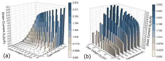
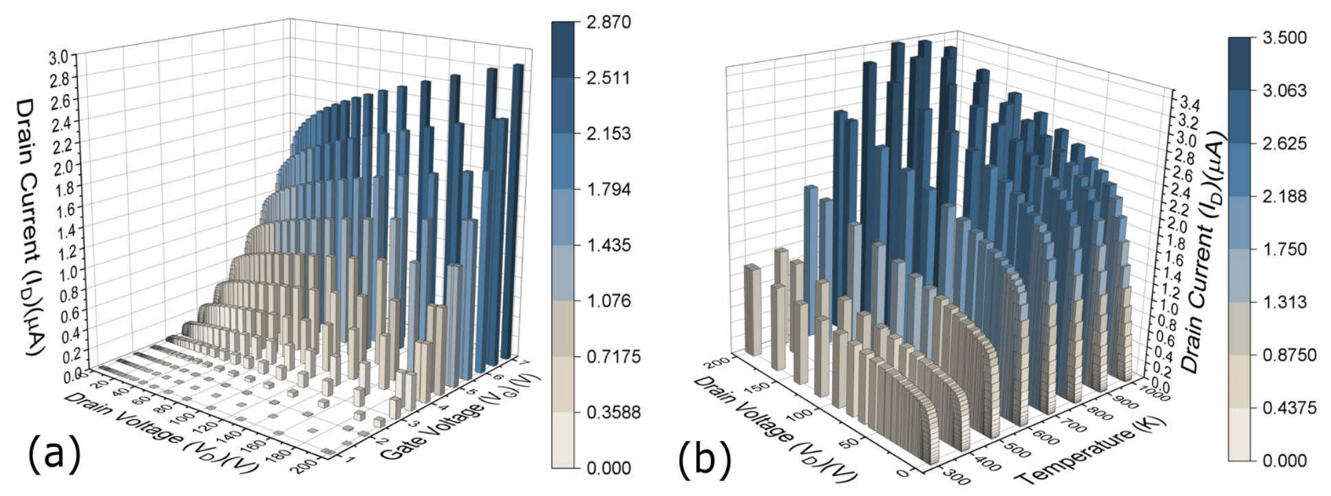
In Figure 4a, the output characteristic curve () of SiC-FET is illustrated for different gate voltages (). The threshold voltage () is 4.45 V and it can be observed that the drain current starts flowing significantly once crosses . The temperature analysis of SiC-FET is carried out from 300 K to 1000 K as depicted in Figure 4b. At = 5 V, the current in SiC-FET increased from 1.11 μA to 3.34 μA with temperature rising from room temperature to 1000 K at = 200 V. There is no breakdown or kink effect observed in the SiC-FET compared to its Si counterpart.
Figure 4.
Output characteristic curve () of SiC-FET at (a) different gate biases (), (b) at temperatures varying from 300 K to 1000 K.
4. SiC Accelerometer: System Simulation
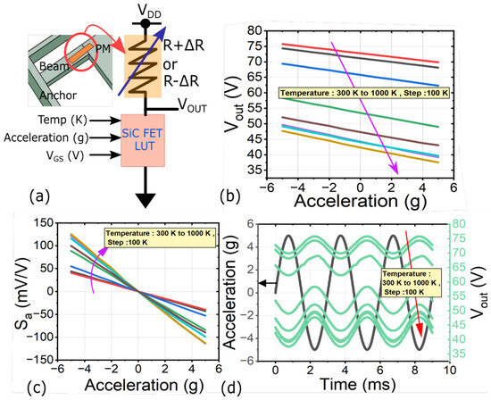
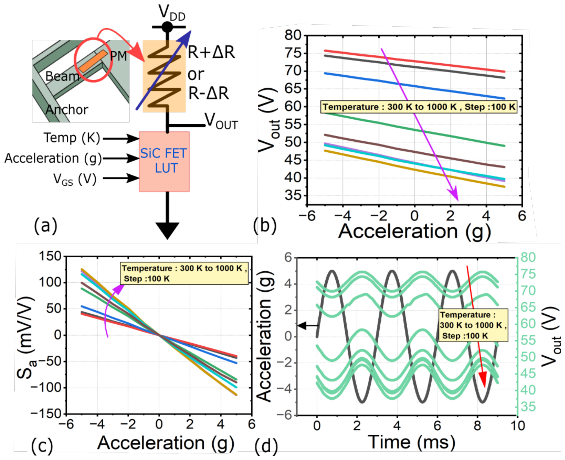
The MEMS FEM and TCAD simulation results are used to model the SiC accelerometer in Cadence Virtuoso using Verilog-A. A single-stage common-source amplifier is designed and simulated to show the feasibility of the proposed monolithic SiC accelerometer with SiC-FET-based circuit readout. The single-stage common-source amplifier with SiC-FET is illustrated in Figure 5a. The inputs to the SiC-FET are the gate voltage and temperature. The acceleration-initiated resistance changes are varied using parametric analysis. The variable resistor represents the beam of the MEMS device as shown in Figure 5a. The supply voltage () and are fixed at 100 V and 7 V, respectively. The output voltage () is taken from the drain terminal of SiC-FET and given as , where is the resistance as a function of acceleration. The DC analysis output is illustrated in Figure 5b at temperatures varying from room temperature (RT) to 1000 K. The is varied from 74.31 V to 68.11 V for −5 g to 5 g acceleration at RT, whereas it varies from 52.10 V to 43.07 V for same acceleration range at 1000 K. The sensitivity of the accelerometer is given as,
Figure 5.
(a) Proposed SiC-FET-based common-source amplifier with piezoresistive load, (b) output voltage vs. acceleration obtained from DC analysis, (c) sensitivity vs. acceleration, (d) transient analysis of proposed accelerometer. The arrow marks indicate that the results are obtained at temperatures ranging from 300 K to 1000 K, with a step size of 100 K.
The sensitivity () vs. acceleration is shown in Figure 5c and it is observed that increases with temperature for a constant acceleration value. At −5 g, is 100 mV/V at 1000 K, which is two times higher than the at RT. Transient analysis of the circuit was carried out and the result is shown in Figure 5d. The non-linearity of the accelerometer is found to be 1%. The acceleration frequency is 328 Hz which is kept sufficiently lower than four times the resonant frequency required for stable accelerometer operation. These results demonstrate the successful integration of the MEMS sensing element with a SiC-FET-based readout circuit, enabling reliable acceleration sensing under extreme high-temperature conditions. The realization of the proposed sensor can be achieved through compatible SiC MEMS bulk micromachining and SiC MOSFET fabrication technologies.
Table 4 summarizes previously reported SiC accelerometers which primarily emphasize sensor design and fabrication, with limited consideration of integrated signal-conditioning electronics. The proposed work distinguishes itself by integrating a 4H-SiC MEMS piezoresistive accelerometer with a SiC-FET readout circuit and validating the complete sensor-readout platform through multi-domain simulations (FEM, TCAD, and Cadence) for operation up to 1000 K.
Table 4.
Comparison of different SiC-based accelerometers.
5. Conclusions
A monolithically integrated SiC MEMS piezoresistive accelerometer with an on-chip SiC-FET readout circuit is designed and fully characterized through FEM, TCAD and circuit-level simulations. The proposed accelerometer has high directional sensitivity along the z-axis, low cross-axis interference and excellent thermal stability over the temperature range of 300–1000 K. The resonant frequency of the proposed accelerometer was 1640 Hz. TCAD simulations showed the high-temperature robustness of the 4H-SiC MOSFET for increasing drain current without breakdown or kink effects up to 1000 K. The successful integration of the MEMS sensing element with a SiC-FET common-source amplifier was demonstrated in the Cadence Virtuoso platform using Verilog-A models derived from FEM and TCAD simulation results. The proposed system achieved an output sensitivity of up to 100 mV/V at 1000 K and exhibited only 1% non-linearity, confirming its suitability for precision sensing in harsh environments. These results demonstrate the potential of single-wafer all-SiC sensor-electronics integration, and offer a promising route towards next-generation intelligent sensing systems for aerospace propulsion, gas turbines, automotive engines, deep-well drilling and other extreme-environment applications. Although this work is limited to multiphysics and circuit-level simulations, experimental fabrication and characterization of the monolithically integrated device, together with optimization of the SiC MEMS–CMOS process flow, will be pursued in future work to validate the proposed design.
Author Contributions
P.M., P.N., and C.M.K.R.: Conceptualization, Data curation, Formal analysis, Investigation, Methodology, Resources, Software, Supervision, Validation, Visualization, Writing—original draft, and Writing—review and editing. A.K.G., B.A., Y.N., and S.B.: Formal analysis, Validation, Visualization, and Writing—review and editing. All authors have read and agreed to the published version of the manuscript.
Funding
Open access funding provided by Manipal Academy of Higher Education, Manipal.
Data Availability Statement
The data analyzed in this study can be obtained from the corresponding author upon reasonable request.
Conflicts of Interest
The authors declare no conflicts of interest.
References
- Huang, X.; Wang, H.; Song, B.; Mao, Y.; Zhao, Z.-J.; Yu, B.; Qian, L. Advances in high-temperature sensor technologies: Material system, sensing principles, drift compensation, and encapsulation reliability. ACS Omega 2026, 11, 4843–4867. [Google Scholar] [CrossRef] [Scilit] [PubMed]
- Aghwariya, M.K.; Goel, T.; Patnaik, A. Advanced materials for RF sensors in harsh environments: A comprehensive review. IEEE Sens. Rev. 2025, 2, 324–338. [Google Scholar] [CrossRef] [Scilit]
- Cheng, Y.; Hua, Y.; Wang, B.; Wang, K.; Tang, W.; Shao, G.; El Sha, W. Multiphysics analysis and simulation of wireless passive temperature and pressure sensors for harsh-environment applications. IEEE J. Multiscale Multiphysics Comput. Tech. 2025, 11, 9–21. [Google Scholar] [CrossRef] [Scilit]
- Fan, J.; Ma, D.; Wang, J.; Chinthavali, M.; Moorthy, R.S.K. Real-time condition monitoring of power modules in grid-tied power converter. In Proceedings of the IEEE Energy Conversion Congress and Exposition (ECCE); IEEE: Detroit, MI, USA, 2022; pp. 1–6. [Google Scholar]
- Guo, X.; Xun, Q.; Li, Z.; Du, S. Silicon carbide converters and MEMS devices for high-temperature power electronics: A critical review. Micromachines 2019, 10, 406. [Google Scholar] [CrossRef] [Scilit] [PubMed]
- Mahissi, M.; Cai, W.; Zhang, X.; Tong, X.; Zhang, C.; Ma, X.; Dossou, M. Diaphragms simulation, fabrication, and testing of a high temperature fiber optic FP accelerometer based on MEMS. Opt. Express 2023, 31, 25025–25041. [Google Scholar] [CrossRef] [Scilit] [PubMed]
- Zhang, Q.; Liu, Y.; Li, H.; Wang, J.; Wang, Y.; Cheng, F.; Han, H.; Zhang, P. A review of SiC sensor applications in high-temperature and radiation extreme environments. Sensors 2024, 24, 7731. [Google Scholar] [CrossRef] [Scilit] [PubMed]
- La Via, F.; Alquier, D.; Giannazzo, F.; Kimoto, T.; Neudeck, P.; Ou, H.; Roncaglia, A.; Saddow, S.E.; Tudisco, S. Emerging SiC applications beyond power electronic devices. Micromachines 2023, 14, 1200. [Google Scholar] [CrossRef] [Scilit] [PubMed]
- Wu, R.; Chen, H.; Zhou, Y.; Guo, Y.; Ji, Z.; Li, L.; Yang, Y.; Wang, G.; Zhou, J.; Fu, Y. Advances in silicon carbides and their MEMS pressure sensors for high temperature and pressure applications. ACS Appl. Mater. Interfaces 2025, 17, 26117–26155. [Google Scholar] [CrossRef] [Scilit] [PubMed]
- Jindal, S.K.; Varma, M.A.; Thukral, D. Study of MEMS touch-mode capacitive pressure sensor utilizing flexible SiC circular diaphragm: Robust design, theoretical modeling, numerical simulation and performance comparison. J. Circuits Syst. Comput. 2019, 28, 1950206. [Google Scholar] [CrossRef] [Scilit]
- Zhang, J.; Chen, J.; Li, M.; Ge, Y.; Wang, T.; Shan, P.; Mao, X. Design, fabrication, and implementation of an array-type MEMS piezoresistive intelligent pressure sensor system. Micromachines 2018, 9, 104. [Google Scholar] [CrossRef] [Scilit] [PubMed]
- Garofalo, A.; Muoio, A.; Belsito, L.; Sapienza, S.; Ferri, M.; Roncaglia, A.; La Via, F. Heteroepitaxial 3C-SiC for MEMS applications. Micromachines 2026, 17, 502. [Google Scholar] [CrossRef] [Scilit] [PubMed]
- Tian, X.; Sheng, W.; Guo, Z.; Xing, W.; Tang, R. Modeling and analysis of a SiC microstructure-based capacitive micro-accelerometer. Materials 2021, 14, 6222. [Google Scholar] [CrossRef] [Scilit] [PubMed]
- Okojie, R.S.; Atwell, A.R.; Kornegay, K.T.; Roberson, S.L.; Beliveau, A. Design considerations for bulk micromachined 6H-SiC high-G piezoresistive accelerometers. In Proceedings of the IEEE International Conference on Micro Electro Mechanical Systems (MEMS); IEEE: Las Vegas, NV, USA, 2002; pp. 618–622. [Google Scholar]
- Liu, W.; Zhao, T.; He, Z.; Ye, J.; Gong, S.; Wang, X.; Yang, Y. The high-efficiency design method for capacitive MEMS accelerometer. Micromachines 2023, 14, 1891. [Google Scholar] [CrossRef] [Scilit] [PubMed]
- Dalal, D.N.; Zhao, H.; Jørgensen, J.K.; Christensen, N.; Jørgensen, A.B.; Bȩczkowski, S.; Uhrenfeldt, C.; Munk-Nielsen, S. Demonstration of a 10 kV SiC MOSFET based medium voltage power stack. In Proceedings of the IEEE Applied Power Electronics Conference and Exposition (APEC); IEEE: New Orleans, LA, USA, 2020; pp. 2751–2757. [Google Scholar]
- Tang, Y.; Guo, J.; Zhu, J.; Liu, Y.; Chang, Y.; Liang, H. Hybrid Laser-ICP micromachining of p-type 4H-SiC piezoresistive elements for high-temperature pressure sensor applications. IEEE Sens. J. 2026, 26, 16775–16780. [Google Scholar] [CrossRef] [Scilit]
- Shao, S. Integrated 4H-Silicon Carbide Diodes and Bridge Circuits for Harsh Environment Applications; University of California, Berkeley: Berkeley, CA, USA, 2016. [Google Scholar]
- Mo, J.; Niu, Y.; May, A.; Rommel, M.; Rossi, C.; Romijn, J.; Zhang, G.; Vollebregt, S. An analog to digital converter in a SiC CMOS technology for high-temperature applications. Appl. Phys. Lett. 2024, 124, 152105. [Google Scholar] [CrossRef] [Scilit]
- Volosov, V.; Bevilacqua, S.; Anoldo, L.; Tosto, G.; Fontana, E.; Russo, A.-L.; Fiegna, C.; Sangiorgi, E.; Tallarico, A.N. Positive bias temperature instability in SiC-based power MOSFETs. Micromachines 2024, 15, 872. [Google Scholar] [CrossRef] [Scilit] [PubMed]
- Martha, P.; Kadayinti, N.; Seena, V. CMOS-MEMS accelerometer with stepped suspended gate FET array: Design and analysis. IEEE Trans. Electron Devices 2021, 68, 5133–5141. [Google Scholar] [CrossRef] [Scilit]
- Martha, P.; Kadayinti, N.; Seena, V. MEMS–suspended gate field effect transistor (SGFET) accelerometer process integration with parylene flexure and plasma doping. J. Micromech. Microeng. 2025, 35, 095004. [Google Scholar] [CrossRef] [Scilit]
- Zhai, Y.; Li, L.; Tao, Z.; Cao, X.; Yang, C.; Che, Z.; Xu, T. Design, fabrication and test of a bulk SiC MEMS accelerometer. Microelectron. Eng. 2022, 260, 111793. [Google Scholar] [CrossRef] [Scilit]
- Liu, C. Foundations of MEMS; Pearson Education India: Noida, India, 2012. [Google Scholar]
- Zhai, Y.; Xu, T.; Xu, G.; Cao, X.; Tao, Z.; Li, H. Temperature characteristics of 4H-SiC substrate and thin-film resistor applied in MEMS piezoresistive sensors. IEEE Sens. J. 2023, 23, 30231–30240. [Google Scholar] [CrossRef] [Scilit]
- Lichtenwalner, D.J.; Park, J.H.; Rogers, S.; Dixit, H.; Scholtze, A.; Bubel, S.; Ryu, S.H. Temperature dependent electrical properties of n-type 4H-SiC substrates. In Materials Science Forum; Trans Tech Publications Ltd.: Bäch, Switzerland, 2023; Volume 1089, pp. 3–7. [Google Scholar]
- Synopsys. Sentaurus Device User Manual; Synopsys, Inc.: Mountain View, CA, USA, 2022. [Google Scholar]
- Atwell, A.R.; Okojie, R.S.; Kornegay, K.T.; Roberson, S.L.; Beliveau, A. Simulation, fabrication and testing of bulk micromachined 6H-SiC high-g piezoresistive accelerometers. Sens. Actuators A Phys. 2003, 104, 11–18. [Google Scholar] [CrossRef] [Scilit]
- Zhai, Y.; Xu, T.; Xu, G.; Cao, X.; Yang, C.; Li, H. Direct Simulation Analysis of Electromechanical Coupling and Joule Heating Effect of a MEMS SiC Piezoresistive Accelerometer. In 2022 9th International Forum on Electrical Engineering and Automation (IFEEA); IEEE: New York, NY, USA, 2022; pp. 969–974. [Google Scholar]

Disclaimer/Publisher’s Note: The statements, opinions and data contained in all publications are solely those of the individual author(s) and contributor(s) and not of MDPI and/or the editor(s). MDPI and/or the editor(s) disclaim responsibility for any injury to people or property resulting from any ideas, methods, instructions or products referred to in the content. |
© 2026 by the authors. Licensee MDPI, Basel, Switzerland. This article is an open access article distributed under the terms and conditions of the Creative Commons Attribution (CC BY) license.