


Abstract
Electromagnetic interference (EMI) shielding is essential in modern electronics, telecommunications, and aerospace systems. Graphite-based materials are promising shielding candidates due to their tunable electrical conductivity, low density, corrosion resistance, and thermal stability. However, numerical studies investigating the combined effects of conductivity and thickness on shielding effectiveness (SE) across the X-band remain limited. This study presents a parametric finite element analysis of EMI shielding performance for graphite materials with electrical conductivities of 1, 10, 100, 1000, and 3000 S/m, representing structures ranging from highly porous to dense graphite. Thicknesses from 1 to 10 mm are simulated in a WR90 rectangular waveguide using finite element simulations. The Transition Boundary Condition (TBC) is employed to efficiently model conductive slabs without resolving the skin depth via volumetric meshing. Shielding effectiveness is evaluated from S-parameters and decomposed into total (SET), absorption (SEA), and reflection (SER) components. Results show that SET increases with both conductivity and thickness, and that shielding behavior is strongly dependent on conductivity. Low-conductivity graphite (σ = 1 S/m) exhibits absorption-dominated shielding, reaching an absorbed power fraction of 89% at 5 mm thickness. At σ = 10 S/m, the material enters a transitional regime where absorption and reflection contribute comparably. For highly conductive graphite (σ ≥ 100 S/m), reflection becomes dominant, with the reflected power fraction approaching 0.97 at σ = 3000 S/m. A conductivity-dependent saturation thickness is identified, beyond which additional thickness provides negligible shielding improvement. Dense graphite materials (σ ≥ 1000 S/m) reach saturation at approximately 1 mm thickness. Finally, a conductivity–thickness design heatmap is developed to guide the optimization of graphite-based EMI shielding materials.
1. Introduction
The rapid expansion of wireless communication technologies has led to an unprecedented increase in the density of electromagnetic devices. 5G networks, satellite communication systems, Internet of Things (IoT) infrastructures, radar platforms, and high-speed digital processors increasingly operate in close proximity, creating environments highly susceptible to electromagnetic interference (EMI) [1]. In safety-critical applications, including aircraft avionics, surgical equipment, and autonomous vehicle sensor systems, the consequences of EMI extend beyond signal degradation and may compromise operational reliability and safety. Consequently, regulatory standards such as IEC 61000-4-3 have imposed increasingly stringent electromagnetic compatibility requirements [2,3], driving the search for lightweight and efficient alternatives to conventional metallic shielding materials.
Traditional metallic shields, such as copper and aluminum, provide excellent shielding effectiveness (SE), often exceeding 60 dB at X-band frequencies, even at moderate thicknesses. However, their high density (approximately 2700–8900 kg/m3), susceptibility to corrosion, thermal expansion mismatch with polymeric composites, and associated weight penalties limit their suitability for aerospace and portable electronic applications [4,5,6]. Carbon-based materials have emerged as promising alternatives because their electrical conductivity can be tailored over a broad range through processing and structural modifications, while maintaining the same chemical composition [7,8,9]. Among these materials, graphite is particularly attractive for its tunable conductivity and structural diversity.
Graphite exists along a continuum of structural forms. Dense, highly ordered graphite exhibits conductivities approaching 104 S/m and is suitable for high-performance EMI shielding applications that require compact geometries [1,10]. In contrast, graphite felt consists of porous fiber networks with conductivities typically ranging from 10 to 300 S/m, depending on fiber packing density and heat-treatment conditions [11,12]. These lightweight and mechanically flexible materials are suitable for applications such as conductive gaskets, textile-based shielding layers, and composite sandwich structures. Intermediate configurations, including compressed graphite felts, expanded graphite compacts, and heat-treated composites, provide additional combinations of conductivity, density, and processability [13], each offering a distinct set of these properties. The SE achieved in any given application depends not just on which grade of graphite is selected, but also on how thick a layer can realistically be accommodated within the design’s geometric and weight constraints [4]. Quantitative understanding of conductivity–thickness interactions is therefore essential for engineering design. For example, an aerospace engineer designing an avionics enclosure must determine whether a lightweight graphite felt layer meets a specified shielding requirement or whether a denser graphite material offers superior performance under the same dimensional constraints. Similarly, compact RF modules in next-generation communication systems impose strict thickness limitations. Existing experimental studies provide valuable data but typically focus on individual materials at fixed thicknesses, making it difficult to establish generalized design guidelines across the conductivity–thickness parameter space [5,6,7,14]. A systematic numerical approach can address this limitation.
Classical EMI shielding theory decomposes total shielding effectiveness into contributions from reflection, absorption, and multiple internal reflections [15,16]. Reflection originates from impedance mismatch at the material interface, whereas absorption results from ohmic dissipation during wave propagation within the material. Internal reflection effects generally become negligible for electrically thick materials [11,17]. Skin depth δ depends on both frequency and conductivity, given by δ = 1/√(πfμ0σ), so for a given sample thickness, the dominant mechanism shifts as conductivity varies. At σ = 10 S/m and 10 GHz, δ ≈ 1.59 mm; a 5 mm sample corresponds to d/δ ≈ 3.14, placing it in the strongly absorbing regime. At σ = 1000 S/m, δ ≈ 0.159 mm; even a 1 mm sample is approximately 6.3 skin depths thick, confirming strongly dominant absorption. It is important to note that the Schelkunoff dB decomposition (SEA = SET − SER) can show SEA ≫ SER in decibels even when the shield physically operates predominantly by reflection, because the dB scale compresses the reflected-power contribution. The physical power balance (R = |S11|2, T = |S21|2, A = 1 – R − T) provides the correct perspective on mechanism dominance. Understanding where each material falls within this regime is essential for interpreting SE measurements and designing simulations [18]. Measured SE data for graphite materials span a wide range. Chung [1] reviews exfoliated graphite (EG) for EMI shielding and reports SE values approaching 130 dB for dense EG non-composites, attributing the performance to the cellular structure’s three-dimensional conductive network. At the other extreme, graphite felt incorporated into an epoxy matrix achieves approximately 60 dB in the X-band [7], with absorption as the dominant mechanism. A multilayer graphite–thermoplastic polyurethane composite (σ in the range of dense graphite) reaches 54 dB for an alternating trilayer geometry totaling about 2.4 mm [14]. Graphite microplatelet structures produced by magnetically assisted 3D printing achieve 40–90 dB in the X-band, depending on filler orientation [4], illustrating how structural anisotropy in graphite-based materials can be used to tune SE directionally.
For comparison, carbon materials with conductivities in the lower graphite-felt range (σ ≈ 1–10 S/m) typically exhibit SE of 20–45 dB at thicknesses of 1–5 mm in the X-band. Kim et al. [19] reported cellulose-derived carbon papers with σ ≈ 5.86 S/m, achieving 43 dB for a single sheet and 72.5 dB for three stacked sheets at 10.5 GHz. The observed non-linear improvement with stacking suggests a saturation behavior similar to the conductivity-dependent trends investigated in the present study. Collectively, these experimental findings highlight the critical roles of both conductivity and thickness; however, they do not provide the systematic multi-parameter datasets required to establish practical conductivity–thickness design guidelines.
Finite element and Finite-Difference Time-Domain (FDTD) simulations have increasingly been applied to EMI shielding problems over the past decade [20,21,22]. COMSOL Multiphysics is among the most widely adopted tools for waveguide-based SE simulation because its RF module provides direct access to S-parameters from physically correct port boundary conditions [23]. A recurring challenge in these studies is the computational cost of resolving the electromagnetic skin depth volumetrically inside the conductive material. At σ = 100 S/m and 10 GHz, the skin depth is approximately 0.503 mm, which requires mesh elements to be well below 0.2 mm throughout the domain. At σ = 1000 S/m, the requirement drops to below 0.05 mm, making volumetric meshing of the conductor effectively intractable for parametric studies on standard hardware.
The Transition Boundary Condition (TBC) resolves this by representing the conductive slab analytically as a surface condition, coupling the tangential fields on both faces through a transfer matrix that encodes the layer’s material properties and thickness. The TBC is accurate for arbitrary ratios of sample thickness to skin depth and has been validated against analytical transfer-matrix solutions to within 1–2 dB [21,22]. It is the only computationally viable approach for a parametric study spanning three orders of magnitude in conductivity and an order of magnitude in thickness, as conducted here.
Beyond graphite, the flexible EMI shielding field also encompasses conductive textiles, in which woven and coated fabrics achieve X-band SE values ranging from approximately 20 dB to over 90 dB, depending on fiber structure and coating type. Densely woven fabrics with a thin metallic coating reach SE values near 80 dB, whereas loosely structured knits show markedly reduced performance due to porosity [24]. Surface-engineering strategies for textile-based shields have diversified considerably beyond simple metallic coatings [25]. Graphite felt shares the fibrous, porous character of these textile shields but derives its conductivity intrinsically rather than from an applied coating, avoiding the delamination and durability losses associated with coated fabrics. The WR90 waveguide transmission/reflection method used here is the standard technique for experimentally characterizing such planar, flexible shields, providing a direct basis for future comparison with textile- and felt-based measurements.
The experimental literature establishes that graphite-based materials can achieve a wide range of SE values, and that both conductivity and thickness are determining factors. What it does not provide is a systematic numerical dataset mapping how SE and its sub-components (SET, SEA, SER) vary continuously across the conductivity–thickness plane for graphite-class materials. Individual experimental studies report one or two data points in this space. No published computational study has performed a full parametric sweep across conductivities spanning from porous graphite felt (σ = 1 S/m) to dense graphite composite (σ = 3000 S/m) at thicknesses from 1 to 10 mm, within a standardized WR90 waveguide geometry. This is the gap the present work fills.
In this work, a COMSOL Multiphysics model of a WR90 rectangular waveguide incorporating a graphite slab through the TBC is developed and validated using empty-waveguide and energy-conservation benchmarks. A comprehensive parametric study is conducted to evaluate total, absorption, and reflection shielding effectiveness (SET, SEA, and SER) across five electrical conductivity levels (1, 10, 100, 1000, and 3000 S/m) and ten material thicknesses (1–10 mm) over the full X-band frequency range (8.2–12.4 GHz), resulting in 1100 frequency-domain simulations. The study further identifies conductivity-dependent saturation thicknesses beyond which additional material yields negligible improvement in SET. In addition, the dominant shielding mechanism, absorption or reflection, is characterized using physical power fractions across the full parameter space, and a design heatmap correlating conductivity and thickness with SET at 10 GHz is presented. The Schelkunoff dB decomposition is employed as a mathematical framework, and its relationship to physical power fractions is explicitly examined.
2. Theoretical Framework and Numerical Modeling Methodology
Shielding effectiveness (SE) quantifies the ability of a material to attenuate the power of an incident electromagnetic wave as it propagates through the medium. In a two-port waveguide configuration, replicated in this simulation, the transmitted signal is measured at Port 2 through the scattering parameter , from which SE is defined as [15,16]:
SET = −20 log10 |S21| (dB)
The negative sign ensures that a weaker transmitted signal—better shielding—produces a larger positive SE value. Total SE can be broken into three physically distinct contributions:
where SER is the loss from reflection at the front surface of the shield, SEA is the ohmic absorption loss as the wave travels through the material, and SEM corrects for energy that bounces back and forth between the two faces of the slab before eventually escaping. Each term can be linked to S-parameters. The reflection loss follows directly from S11 [17]:
and the absorption loss is then recovered as the remainder:
SET = SER + SEA + SEM
SER = −10 log10 (1 − |S11|2) (dB)
SEA = SET − SER (dB)
The multiple-reflection term warrants careful consideration, as it is often neglected without explicit justification. Physically, is negative, thereby reducing the total shielding effectiveness. It becomes significant only when the wave has not been sufficiently attenuated within the material before reaching the rear interface. A commonly accepted criterion is that can be neglected when exceeds approximately 15 dB [17]. In the present study, SEA is below 15 dB for σ = 1 S/m at thicknesses d ≤ 4 mm (d/δ ≤ 0.79 at 10 GHz) and for σ = 10 S/m at d ≤ 1 mm (d/δ ≤ 0.63). For this subset of cases, SEM contributes a small negative correction that tends to offset some of the SER. Across the remaining parameter space, it is negligible and is set to zero throughout. This is consistent with how the multiple-reflection correction is treated in the experimental literature for materials of comparable conductivity [11,26]. It is also useful to frame the results in terms of power fractions. Defining R = |S11|2 (reflected power fraction) and T = |S21|2 (transmitted fraction), the absorbed fraction follows as A = 1 − R − T. Energy conservation requires A ≥ 0 everywhere, which serves as a straightforward simulation sanity check. For a passive, non-active material, A + R + T = 1 must hold at every frequency and for every parameter combination. This condition was verified for all 1100 solutions in this study.
The electromagnetic skin depth δ defines how quickly a plane wave decays inside a conducting medium. Specifically, it is the depth at which the wave amplitude falls to 1/e of its surface value:
where f is frequency, μ0 is the permeability of free space (4π × 10−7 H/m), and σ is electrical conductivity. This formula is the standard plane-wave good-conductor approximation and is accurate when σ/(ωε0) ≫ 1. For σ = 1 S/m at 10 GHz, this ratio is approximately 1.8, meaning the formula slightly underestimates the actual skin depth. For σ ≥ 10 S/m, the approximation is adequate for engineering purposes. The ratio d/δ determines which shielding regime the material operates in. When d/δ ≫ 1, the shield is electrically thick: the wave is heavily attenuated within the material, and SEA dominates. When d/δ ≪ 1, the electrically thin limit, ohmic absorption is weak and reflection at the two surfaces carries most of the shielding burden. Between these extremes lies a transition region where both mechanisms contribute.
δ = 1/√(π f μ0 σ) (m)
Table 1 lists the calculated skin depth for each of the five conductivity levels studied, at three representative X-band frequencies. For σ = 1 S/m (highly porous graphite), δ ≈ 5.03 mm at 10 GHz. Sample thicknesses from 1 to 4 mm lie in the electrically thin regime (d/δ < 1), while thicknesses from 5 to 10 mm span the transition to intermediate absorption (d/δ up to 2.0). The entire parametric range at this conductivity, therefore, spans both the thin and transition regimes. For σ = 10 S/m, δ ≈ 1.59 mm, so a 5 mm sample represents d/δ ≈ 3.14—firmly in the strongly absorbing regime. A 10 mm sample at σ = 10 S/m has d/δ ≈ 6.29, placing it well into the saturation approach zone. At σ = 1000 S/m, δ ≈ 0.159 mm, so even the 1 mm sample is approximately 6.3 skin depths thick, and absorption is strongly dominant; additional thickness produces negligible returns. This is the saturation behavior, which is quantified later in this work.
Table 1.
Electromagnetic skin depth (mm) calculated from Equation (5) for the five conductivity levels at three X-band frequencies (μr = 1 for all graphite forms).
One further implication of skin depth concerns the simulation strategy. At σ = 100 S/m and 10 GHz, the skin depth is approximately δ ≈ 0.503 mm, which would require volumetric mesh elements significantly smaller than 0.2 mm in the conductive region to accurately resolve the field decay. For σ = 1000 S/m, this requirement becomes even more stringent, dropping below approximately 0.016 mm. Resolving a full graphite slab with dimensions 10 mm × 22.86 mm × 10.16 mm at such resolutions would require tens of millions of elements and memory on the order of several hundred gigabytes. Consequently, the TBC introduced in the subsequent section is not merely a computational convenience but a necessity for enabling a feasible and efficient parametric study over the full range of conductivity and thickness.
The TBC is a surface impedance model that analytically represents the electromagnetic effects of a conductive layer without requiring the layer to be meshed as a three-dimensional domain. Its mathematical foundation lies in the transfer matrix method for a planar slab [22,27]. For a layer of thickness d with material parameters (σ, εr, μr), the transfer matrix relates the tangential electric and magnetic fields on the two surfaces of the layer. The TBC converts this matrix into a pair of surface admittance conditions, coupling the fields on each face through the layer’s frequency-dependent response—without solving any equations inside the layer itself. COMSOL implements this as a boundary condition applied to an interior surface, doubling the number of unknowns on that boundary to account for the electric field on each face separately [21].
Two properties of TBC are particularly relevant here. First, it is valid for arbitrary ratios of d/δ, including both the electrically thin limit (d ≪ δ) and the electrically thick limit (d ≫ δ). This is not self-evident: the better-known impedance boundary condition (IBC) becomes inaccurate when d is comparable to or smaller than δ, because it assumes the wave decays completely within the layer before reaching the rear face. The TBC carries no such restriction [21,22]. Second, the physical thickness d entered in the TBC settings is independent of the geometric thickness of the boundary in the mesh. In this study, the geometry includes a 0.5 mm placeholder slab whose sole function is to define the boundary location and orientation; the actual physical thickness, varied from 1 to 10 mm in the parametric sweep, is passed to the TBC as a parameter. This decoupling between geometric and physical thickness is what makes the parametric study computationally tractable. Karlsson [27] provides a rigorous derivation of approximate boundary conditions for thin structures of this type, showing that, for smooth boundaries and layers that satisfy standard regularity conditions, the transfer-matrix approach yields field solutions accurate to within a few percent of the exact volumetric solution. Senior and Volakis [22] extend this treatment to a broader class of boundary geometries. In COMSOL’s RF module implementation, the TBC has been validated against analytical solutions for flat conductive layers, with errors reported to be below 2 dB across a wide range of conductivity and thickness combinations [21,22]. This is the required accuracy level for the present study, where SE values range from approximately 10 dB to over 200 dB across the parametric space.
A rectangular waveguide provides a controlled electromagnetic environment well suited to SE measurement and simulation. The WR90 standard specifies an inner cross-section of 22.86 mm (broad wall, a) by 10.16 mm (narrow wall, b). The dominant propagating mode is TE10, with a cutoff frequency of fc = c/(2a) = 6.56 GHz. The standard operating band is 8.2 to 12.4 GHz, which lies safely above the cutoff and below the onset of the next higher-order mode TE20 at 13.1 GHz. All simulations in this study are carried out within this band, ensuring single-mode propagation throughout [18]. In the TE10 mode, the electric field is polarized along the y-direction (the narrow wall direction) and varies sinusoidally across the broad wall over a single half-period, reaching zero at the metallic walls. There is no field variation in the propagation direction z beyond the traveling-wave phase factor. This field distribution couples well to a planar sample placed perpendicular to z, because the field is spatially uniform across the sample face and presents a well-defined impedance to the incoming wave. The two-port S-parameter measurement from this configuration—one port exciting the mode, the other acting as a matched load—directly mirrors the experimental VNA setup used in waveguide SE measurements [28], making the simulation immediately comparable to physical measurements without requiring correction factors.
Wave propagation inside the guide is governed by the vector Helmholtz equation derived from Maxwell’s equations under time-harmonic excitation:
where k0 = ω√(μ0ε0) is the free-space wavenumber and the term in parentheses is the complex relative permittivity of the medium. The imaginary part, jσ/ωε0, accounts for ohmic loss: at 10 GHz and σ = 100 S/m, this term is approximately 180, far exceeding the real part εr = 12. This confirms that the material is loss-dominated at this conductivity, and that the precise value of εr has relatively little influence on the result. For the lower conductivities (σ = 1 and 10 S/m), jσ/ωε0 is of comparable magnitude to εr, meaning both the real and imaginary parts of the permittivity contribute to the wave behavior. COMSOL solves Equation (6) using the Electromagnetic Waves, Frequency Domain (emw) interface, which applies the finite element method on an unstructured tetrahedral mesh.
∇ × (μr−1 ∇ × E) − k02 (εr − jσ/ωε0) E = 0
3. Simulation Configuration and Numerical Verification
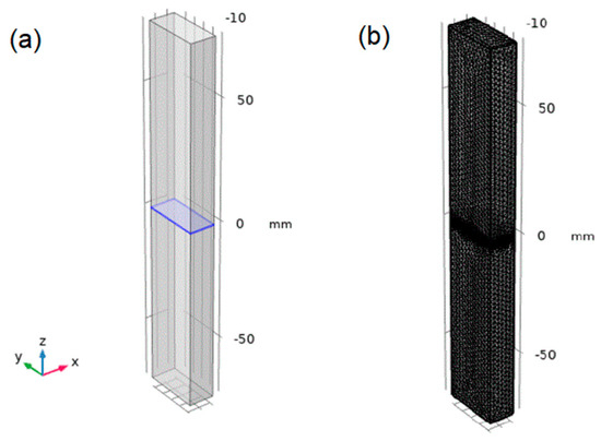
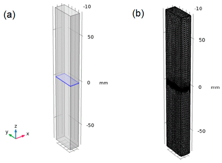
All simulations were performed in COMSOL Multiphysics 5.6 using the RF Module Electromagnetic Waves, Frequency Domain (emw) interface, which solves Equation (6) on an unstructured tetrahedral mesh. The simulated geometry is a WR90 waveguide with inner dimensions of 22.86 × 10.16 mm2 and a total length of 150 mm, as shown in Figure 1a. The graphite sample slab is centered at z = 75 mm, flanked by two air domains each 72.75 mm long—approximately 1.5 guided wavelengths at 8.2 GHz—ensuring full attenuation of evanescent port modes before they interact with the sample interface. The sample is represented as a surface via the TBC; its nominal geometric thickness is 0.5 mm, while the physical thickness (d) is specified parametrically through the TBC settings and varied from 1 to 10 mm. The Form Union operation merges all domains, ensuring field continuity across internal boundaries.
Figure 1.
A 3D view of the WR90 waveguide simulation geometry, showing the two air domains flanking the centered graphite sample slab. (a) Full waveguide with the sample at the midpoint and port locations at each end. (b) Tetrahedral mesh distribution.
Two numeric waveguide ports are applied at z = 0 (Port 1, excitation on, Pin = 1 W) and z = 150 mm (Port 2, passive matched termination). The numeric port type computes the TE10 mode profile using boundary mode analysis at 10 GHz prior to the frequency-domain solve. This two-port arrangement directly mirrors a VNA measurement, providing access to S11 and S21. The four longitudinal waveguide walls are assigned the Perfect Electric Conductor (PEC) condition. The graphite slab is represented by the TBC applied to its two z-facing surfaces. No perfectly matched layers are required as the closed metallic waveguide confines all fields within the simulation domain. The five conductivity values span the full structural range of graphite: σ = 1 S/m (highly porous graphite foam), 10 S/m (low-density graphite felt), 100 S/m (commercial-grade graphite felt), 1000 S/m (dense or heat-treated graphite composite), and 3000 S/m (dense graphite composite, compressed or heat-treated) [12]. Relative permittivity εr = 12 is adopted for all conductivity levels, consistent with published values for carbon-based materials at GHz frequencies [10]. Relative permeability μr = 1 throughout. Table 2 summarizes all simulation parameters.
Table 2.
Summary of simulation parameters used in the COMSOL Multiphysics parametric study.
Graphite felt is typically manufactured through the controlled carbonisation and graphitisation of polyacrylonitrile (PAN) or rayon precursor fibers at temperatures ranging from 1000 °C to 3000 °C. The degree of graphitization, fiber packing density, and heat treatment temperature are the primary factors controlling the final electrical conductivity of the felt. Low-temperature processing yields highly porous, low-conductivity felts (σ = 1–10 S/m), while high-temperature treatment and mechanical compression progressively increase conductivity toward the dense graphite range (σ = 100–3000 S/m). This manufacturing continuum directly maps onto the parametric conductivity range studied in this work, confirming that the conductivity values selected span the full spectrum of commercially achievable graphite felt grades. It should be noted, however, that porosity and density are not the sole determinants of conductivity: heat-treatment temperature and fiber alignment can independently raise or lower the effective bulk conductivity, so the σ values studied here represent achievable effective conductivity rather than a strict density hierarchy.
A user-controlled free tetrahedral mesh is applied to the air domains, with a maximum element size of 2 mm and a minimum of 0.5 mm, providing λ/12 resolution at 12.4 GHz, as shown in Figure 1b. The TBC eliminates the need to mesh within the graphite domain, removing the skin-depth-resolution burden entirely. The model contains approximately 100,000 tetrahedral elements and 668,000 degrees of freedom. Mesh convergence was verified at σ = 10 S/m, d = 5 mm, f = 10 GHz; the SET change between the current mesh and a 50–refined mesh was less than 0.5 dB. Table 3 summarizes the convergence results. For Model Validation, four validation checks were performed before production runs. First, the empty waveguide test confirmed S21 = 0.00 dB and S11 at the double-precision numerical noise floor of the solver (≈ −300 dB, |S11|2 ≈ 10−30) across the full X-band, the practical equivalent of the theoretical S11 = −∞ dB for a perfectly matched port, verifying correct port setup and PEC boundary conditions. Second, the energy conservation condition |S11|2 + |S21|2 ≤ 1 was satisfied for all 1100 parametric solutions. Third, SET increased monotonically with thickness for all σ ≥ 10 S/m; a minor non-monotonicity at σ = 1 S/m, d = 2 mm. Fourth, COMSOL SET values at σ = 10 S/m were compared with the analytical transfer-matrix solution, with agreement within 2 dB across all thicknesses, confirming TBC accuracy.
Table 3.
Mesh convergence study at σ = 10 S/m, d = 5 mm, f = 10 GHz.
4. Results and Discussion
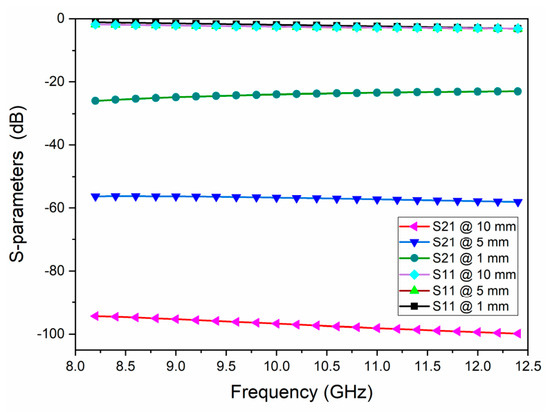
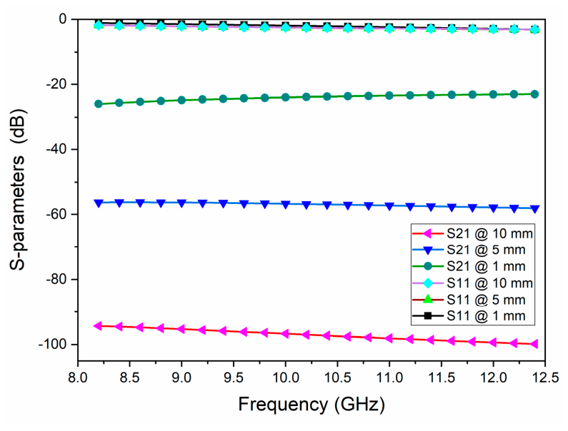
The primary outputs of each COMSOL frequency-domain simulation are the complex S-Parameters S11 and S21, which represent the reflection and transmission of the graphite sample interface. Figure 2 shows the S-parameters as a function of frequency for the electric conductivity of 10 S/m (representative of porous graphite felt) at three thicknesses of 1, 5, and 10 mm.
Figure 2.
S11 and S21 (dB) versus frequency (8.2–12.4 GHz) for σ = 10 S/m (porous graphite felt) at d = 1, 5, and 10 mm.
As shown in Figure 2, S21 becomes progressively more negative as the thickness increases, directly reflecting increased absorption in the thicker graphite layer. The S21 curves decrease by approximately 8 dB per mm of additional thickness in the 1–5 mm range, consistent with linear absorption scaling in the regime where d is comparable to the skin depth [18]. For σ = 10 S/m at 10 GHz, the skin depth is δ ≈ 1.59 mm. The S11 curves remain approximately constant at −1.8 to −3.1 dB across the X-band for all three thicknesses, corresponding to a reflected power fraction R = |S11|2 of approximately 0.49–0.67, confirming that σ = 10 S/m operates in a transitional regime where reflection and absorption are comparable. Rather than any intrinsic material resonance, this slight fluctuation represents the frequency dependence of the guided wave impedance in the WR90 waveguide [18].
The observed S-parameter trends can be physically interpreted straightforwardly for porous graphite. At a conductivity of σ = 10 S/m, the skin depth at 10 GHz is approximately 1.59 mm. For a 1 mm-thick sample (d/δ ≈ 0.63), the material is electrically thin, allowing partial penetration of the incident electromagnetic wave. In this regime, both transmission and internal absorption contribute significantly to wave attenuation. In contrast, for a 10 mm-thick sample (d/δ ≈ 6.29), the material becomes electrically thick and strongly absorbing, such that the incident wave is almost entirely attenuated within the bulk before reaching the rear interface. The near-constant S11 across all thicknesses indicates that the front-surface reflection is governed primarily by the intrinsic surface impedance of the graphite, which depends on material properties such as conductivity and permittivity, rather than on geometric thickness. Consequently, increasing sample thickness has a negligible influence on the reflection coefficient, even though it strongly affects transmission and absorption behavior [15,17]. This behavior is fundamentally different from that of dense metallic shields, where the extremely low surface impedance leads to a strong impedance mismatch with free space. As a result, even very thin metallic layers can exhibit high reflectivity (large S11), with electromagnetic energy reflected rather than penetrating the material [15].
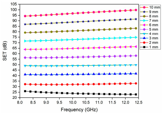
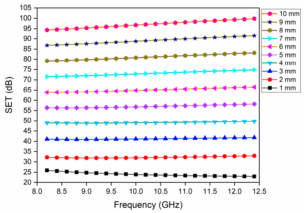
Figure 3 presents SET as a function of frequency across the full X-band for σ = 10 S/m at all ten thickness values from 1 to 10 mm. This figure directly illustrates the two key findings for porous graphite: the strong thickness dependence of shielding performance and the broadband character of the shielding across the X-band. At σ = 10 S/m, SET ranges from approximately 24 dB at 1 mm to approximately 97–100 dB at 10 mm, representing a 73 dB increase in SET for a ten-fold increase in thickness. This near-linear scaling in dB is consistent with the skin depth analysis: with δ ≈ 1.59 mm at this conductivity, thicknesses from 1 to 10 mm span d/δ from 0.63 to 6.29, placing the system in a regime where SEA scales approximately linearly with d/δ and therefore with thickness [17]. The slight positive frequency slope visible in each SET curve (SET increases by 2–5 dB across 8.2–12.4 GHz) is explained by the decreasing guided wavelength at higher frequencies, which increases the effective electrical thickness of the sample relative to the local wavelength [18]. This broadband uniformity is a practical advantage of graphite felt as a shielding material, as it requires no frequency-specific tuning [7].
Figure 3.
SET (dB) versus frequency (8.2–12.4 GHz) for σ = 10 S/m (porous graphite felt) at ten thickness values from 1 mm to 10 mm.
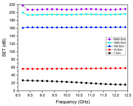
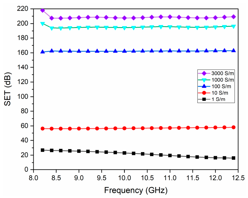
Figure 4 provides a complementary view at a fixed thickness of 5 mm across all five conductivity levels, illustrating the dominant role of conductivity in determining the absolute SE level. Figure 4 demonstrates that the effect of conductivity on SET at a fixed thickness of 5 mm is profound. At σ = 1 S/m (highly porous graphite), SET is approximately 22 dB, barely meeting the minimum requirements for commercial EMI shielding [6]. At σ = 10 S/m (porous graphite felt), SET increases to approximately 57 dB, sufficient for most electronic applications [6]. At σ = 100 S/m (medium-density graphite felt), SET rises sharply to approximately 162 dB, far exceeding any practical shielding requirement. At σ = 1000 and 3000 S/m (dense graphite), SET reaches approximately 194 and 207 dB, respectively, values so large that the 5 mm thickness is grossly excessive for practical purposes. Notably, the curves for σ = 1000 and 3000 S/m are nearly identical, indicating that the transition from dense graphite felt to solid graphite provides very little additional shielding benefit at this thickness—a direct consequence of the saturation effect discussed in the following subsection. The σ = 1 S/m curve (highly porous graphite) shows a slight negative frequency slope, with SET decreasing slightly as frequency increases. This is physically explained by the increasing skin-depth mismatch at higher frequencies: as frequency increases, the guided wavelength shortens, while the skin depth decreases [18]. For very low-conductivity materials, the sample remains electrically thin across the entire frequency band, and the frequency-dependent impedance of the waveguide mode slightly reduces coupling to the material at higher frequencies, resulting in a marginally lower SE. This crossover from a positive to a negative frequency slope as conductivity decreases from 10 to 1 S/m is a subtle yet physically meaningful observation that distinguishes porous graphite from denser forms of graphite.
Figure 4.
SET (dB) versus frequency (8.2–12.4 GHz) for d = 5 mm at all five conductivity values (1, 10, 100, 1000, 3000 S/m).
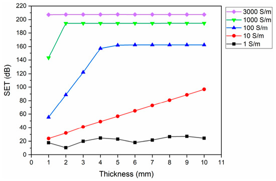
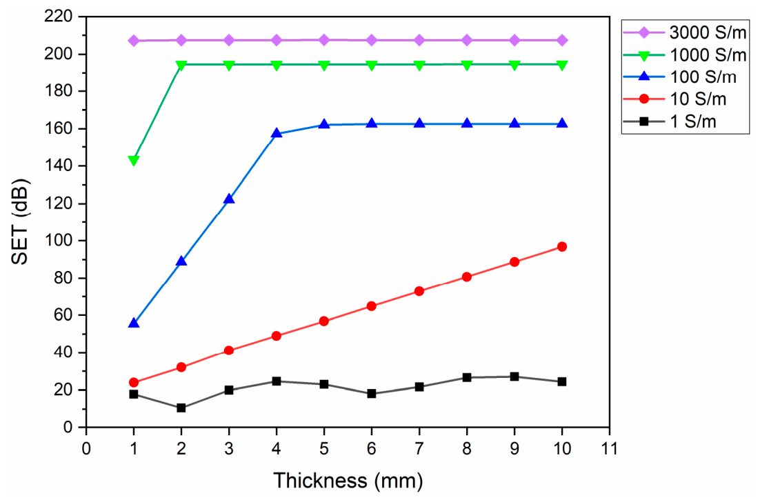
Figure 5 shows SET as a function of sample thickness at a fixed frequency of 10 GHz for all five conductivity values. This figure most clearly reveals the two distinct regimes of graphite shielding behavior that distinguish porous from dense graphite structures. Two physically distinct regimes are visible in Figure 5. The first is a linear growth regime, exemplified by the σ = 10 S/m curve (porous graphite felt), where SET increases approximately proportionally with thickness from 24 dB at 1 mm to 97 dB at 10 mm. This linear behavior arises because each additional millimeter of graphite felt contributes approximately the same incremental absorption, as the material is not yet electrically thick enough for the wave to be fully attenuated [15,17]. The second is a saturation regime, observed for σ > 100 S/m (dense graphite), where SET rises steeply at low thicknesses and then plateaus at a relatively constant value as thickness increases. The physical origin of saturation is straightforward. For medium-density graphite with σ = 100 S/m, the skin depth at 10 GHz is δ ≈ 0.503 mm. The saturation threshold (d/δ ≈ 3), therefore, occurs at approximately d ≈ 1.5 mm [15]. A 4 mm sample represents d/δ ≈ 7.95, meaning the wave amplitude is attenuated by a factor of e−7.95 ≈ 3.5 × 10⁻⁴ before reaching the rear surface. Adding more graphite beyond the saturation thickness simply adds weight and cost without improving shielding performance. For σ = 1000 S/m (δ ≈ 0.159 mm), saturation occurs near d ≈ 0.5 mm; for σ = 3000 S/m (δ ≈ 0.0919 mm), saturation occurs near d ≈ 0.3 mm. Any practical sample thickness of a dense graphite composite already exceeds the saturation threshold by a wide margin.
Figure 5.
SET (dB) versus sample thickness (1–10 mm) at 10 GHz for all five conductivity values.
A minor anomaly is observed in the σ = 1 S/m curve, which shows a non-monotonic dip in SET near d = 2 mm. This behavior is consistent with a waveguide resonance effect: at very low conductivities, the graphite sample is nearly transparent, and the sample acts as a low-Q resonant cavity within the waveguide [18]. The round-trip phase condition for resonance requires 2d·βg = 2nπ, where βg is the phase constant inside the graphite. For σ = 1 S/m, a rough estimate gives βg ≈ βair (since the material is nearly transparent), and with βair ≈ 1580 rad/m at 10 GHz, the first resonance (n = 1) occurs at d ≈ π/βair ≈ 2.0 mm, consistent with the observed dip. This is not a numerical artifact but a genuine physical effect. The same phenomenon has been reported in analytical transfer matrix studies of low-conductivity dielectric slabs in waveguides and is a distinguishing characteristic of the very low conductivity (highly porous) limit of graphite materials [22,27].
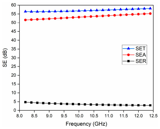
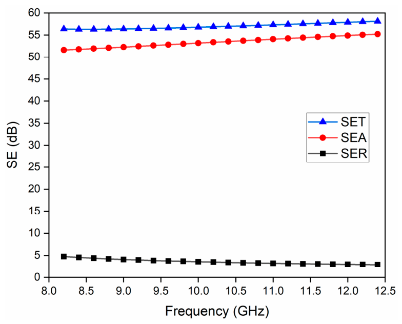
The decomposition of SET into its absorption (SEA) and reflection (SER) components provides the most physically illuminating perspective on graphite shielding behavior across the full porosity spectrum. Figure 6 shows this decomposition as a function of frequency for the representative case of σ = 10 S/m (porous graphite felt) at d = 5 mm.
Figure 6.
SET, SEA, and SER (dB) versus frequency (8.2–12.4 GHz) for σ = 10 S/m and d = 5 mm.
Figure 6 unambiguously shows that absorption dominates reflection for porous graphite felt across the entire X-band. SEA accounts for approximately 93% of SET (approximately 52–55 dB out of 57 dB total) at σ = 10 S/m and d = 5 mm, while SER contributes only 3–5 dB. However, this apparent dominance of SEA in the dB scale must be interpreted carefully against the physical power balance for σ = 10 S/m: the absorbed power fraction A ≈ 0.33–0.51 and R ≈ 0.49–0.67, confirming that σ = 10 S/m at d = 5 mm operates in a transitional regime where neither mechanism fully dominates. Genuine absorption dominance in the power balance is observed at σ = 1 S/m at higher frequencies, where A reaches 0.89 [26]. Both SEA and SER are relatively flat with frequency, confirming the broadband nature of graphite as an EMI shield [7]. For σ = 10 S/m at d = 5 mm, R ranges from approximately 0.49 to 0.67 across the X-band, confirming the transitional character of this conductivity grade.
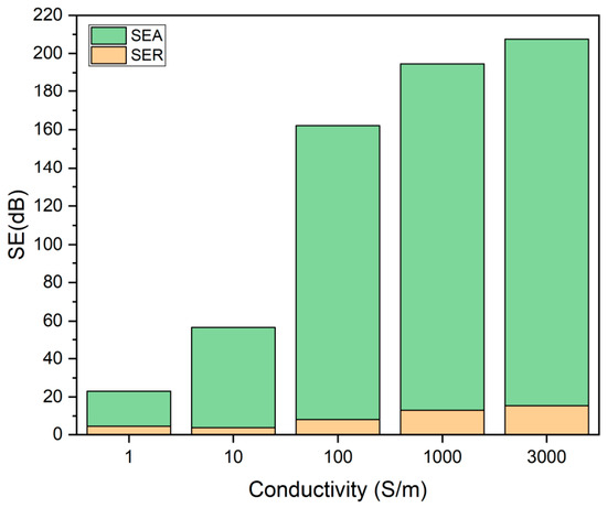
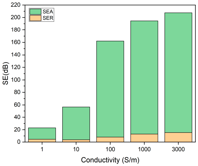
Figure 7 presents a bar chart comparing SEA and SER for all five conductivity levels at d = 5 mm and 10 GHz, providing a systematic view of how the absorption–reflection balance evolves as graphite transitions from porous to dense structures.
Figure 7.
SEA (green) and SER (orange) contributions to SET for all five conductivity values at d = 5 mm and 10 GHz. SEA exceeds SER in dB across all conductivity levels and grows faster than SER as conductivity increases; this dB-domain dominance is a logarithmic-scale artifact rather than a reflection of the physical power balance.
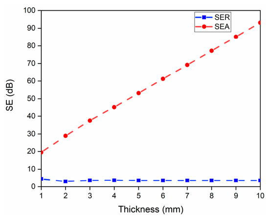
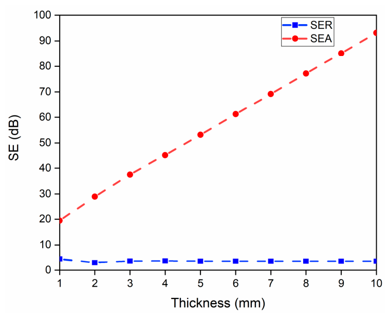
The stacked bar chart in Figure 7 shows how SER increases with conductivity, from approximately 4 dB at σ = 1 S/m to approximately 15 dB at σ = 3000 S/m. This moderate increase reflects the growing impedance mismatch at the air–graphite interface as the material becomes denser and more conductive [15]. SEA increases dramatically with conductivity, driven by exponential increases in ohmic dissipation. However, the apparent dominance of SEA in dB across all conductivity levels (Figure 7) must be interpreted with caution [26]. The physical reflected power fraction R = |S11|2 approaches 0.97 at σ = 3000 S/m—meaning 97% of incident power is physically reflected, not absorbed. The dB decomposition yields large SEA values as an artifact of the logarithmic scale, not because absorption is the primary power mechanism for dense graphite [26]. It is worth noting that SEA/SER and SEA/SET ratios reported in the dB domain carry genuine comparative value for σ ≤ 10 S/m, where the dB decomposition and the physical power balance agree. Caution is warranted only when extending these ratios to highly conductive materials (σ ≥ 100 S/m), where the logarithmic scale can misrepresent the dominant physical mechanism. At σ = 1–10 S/m, absorption genuinely dominates in both dB decomposition and physical power fractions. At σ ≥ 100 S/m, the dB decomposition and physical power balance give opposite conclusions; only the power balance provides the physically correct picture. Figure 8 provides a complementary view of how SEA and SER depend on thickness at a fixed conductivity (σ = 10 S/m), offering numerical simulation evidence that distinguishes the volumetric nature of absorption from the surface nature of reflection.
Figure 8.
SEA and SER versus sample thickness (1–10 mm) at σ = 10 S/m and 10 GHz.
Figure 8 provides definitive numerical evidence from simulations distinguishing the two mechanisms. SEA grows linearly with thickness, from approximately 20 dB at 1 mm to approximately 92 dB at 10 mm, consistent with the predicted linear scaling with d/delta in the intermediate absorption regime [17]. SER, in contrast, remains approximately constant at 3–4 dB across the entire thickness range, confirming that it is a purely surface effect governed by the air–graphite impedance mismatch and entirely independent of the amount of graphite beneath the surface [15,16]. This independence means that increasing the thickness of a graphite shield never reduces the surface reflection loss; it only increases absorption [15]. For porous graphite felt, where the reflection contribution is already small, the designer’s primary tools are thickness and/or conductivity enhancements to increase SEA.
The results of the parametric study can be synthesized into practical engineering guidelines for selecting graphite shielding materials. The fundamental design principle emerging from this study is that, for low-conductivity graphite (σ ≤ 10 S/m), absorption dominates in both the dB decomposition and the physical power fractions, making thickness the primary design lever. For high-conductivity graphite (σ ≥ 100 S/m), the shield operates predominantly by reflection in terms of physical power, and saturation of SET occurs at very small thicknesses—below 1.5 mm for σ = 100 S/m, below 0.5 mm for σ = 1000 S/m, and below 0.3 mm for σ = 3000 S/m. Beyond these thresholds, additional material adds weight and cost without any measurable improvement in shielding performance.
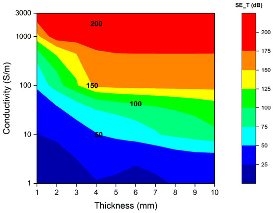
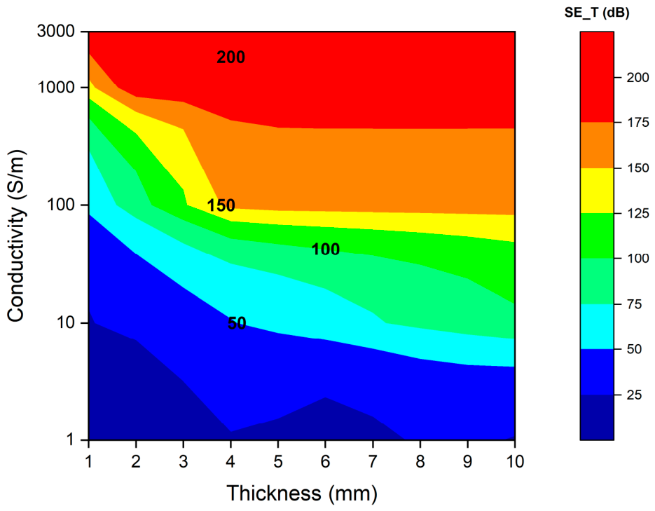
Figure 9 presents the SET design heatmap over the full parameter space of electrical conductivity (1–3000 S/m, log scale) and sample thickness (1–10 mm) at a reference frequency of 10 GHz. Four iso-SE contours are overlaid at 50, 100, 150, and 200 dB to guide engineering interpretation. The simulated SET values range from approximately 10 dB in the lower-left corner to 207 dB in the upper region, spanning nearly the full practical spectrum of graphite shielding behavior. For σ ≥ 100 S/m, the displayed SET values in the saturation zone exceed the dynamic range of standard VNA-based measurement systems, which are typically limited to 80–120 dB [28]. The values of 162 dB (σ = 100 S/m), 194 dB (σ = 1000 S/m), and 207 dB (σ = 3000 S/m) represent confirmed theoretical lower bounds derived from the TBC transfer matrix formulation and should be interpreted as such: they confirm that the bulk material imposes no practical upper limit on shielding performance in these regimes, and that system-level factors, joints, apertures, seams, and instrument dynamic range, become the sole limiting factors [26]. The key design information—the saturation threshold and the contour shapes—is physically reliable and is the primary design information the heatmap is intended to convey.
Figure 9.
SET design heatmap showing SET (dB) as a function of sample thickness (x-axis, 1–10 mm) and electrical conductivity (y-axis, log scale) at 10 GHz. Iso-SE contours at 50, 100, and 150 dB are overlaid.
Three distinct performance zones are visible. In Zone 1 (lower-left region, σ < 10 S/m and d < 4 mm), SET remains below 50 dB, and the shield is inadequate for most applications; this zone corresponds to highly porous graphite structures in which neither the intrinsic conductivity nor the sample thickness provides sufficient absorption depth [6]. A notable SET dip is observed near d ≈ 2 mm at the lowest conductivity (σ = 1 S/m), consistent with the Fabry–Pérot resonance. Designers working with low-conductivity grades should avoid this thickness range if consistent broadband shielding is required. In Zone 2 (middle region, σ between approximately 10 and 300 S/m), SET spans 50–150 dB, covering the range required for most commercial and industrial electronics applications [6]; graphite felt in this conductivity range at thicknesses of 2–10 mm falls within this zone, with the 100-dB contour—crossed at approximately 7 mm for σ = 10 S/m and at approximately 1.5 mm for σ = 100 S/m—acting as a practical benchmark for many shielding specifications. In Zone 3 (upper region, σ > 300 S/m), SET reaches or exceeds 200 dB even at modest thicknesses above 1–2 mm, providing performance well beyond any practical commercial requirement regardless of the specific value.
The flat color regions in the upper portion of the heatmap correspond to the saturation zones identified in the following section. For σ = 100 S/m, saturation occurs near d ≈ 1.5 mm; for σ = 1000 S/m, near d ≈ 0.5 mm; and for σ = 3000 S/m, near d ≈ 0.3 mm. Beyond these thicknesses, additional material adds weight and cost without improving SET. The steep color gradient in the lower-left corner reflects the extreme sensitivity of porous graphite shielding to small changes in either conductivity or thickness, which has important implications for the manufacturing control of graphite felt: even small variations in fiber density or porosity can produce large changes in SE performance for low-conductivity grades [12]. Conversely, the relatively gradual color transition across the mid-conductivity range (10–100 S/m) indicates that thickness can serve as a reliable compensating parameter in this regime, offering a practical engineering lever when conductivity cannot be precisely controlled. Table 4 serves as a structured summary of the simulation data presented in Figure 9 (the SET design heatmap). It synthesizes key total shielding effectiveness (SET) values (at 1 mm, 5 mm, and 10 mm) and highlights the saturation thickness across all five evaluated graphite conductivity levels.
Table 4.
SET summary table at 10 GHz for selected conductivity-thickness combinations.
These results translate into the following practical design guidelines for graphite-based EMI shielding. For applications requiring SET below 50 dB, highly porous graphite (σ = 1–10 S/m) with thicknesses of 1–10 mm is sufficient and offers the lightest option [6]. The principal advantage of porous graphite in this regime is its very low areal density and high gas permeability, making it suitable for ventilated electronic enclosures or thermally managed shields [13]. However, designers should be aware of the localized performance dip observed around 2–3 mm thickness at the lowest conductivity values, where the Fabry–Pérot resonance produces a localized SET reduction that could place the shield below specification in a narrow frequency sub-band, which suggests that this thickness range should be avoided for low-conductivity grades if consistent shielding is required.
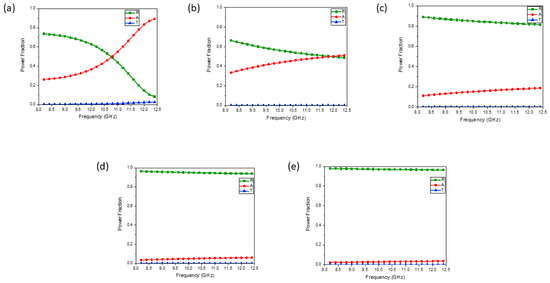
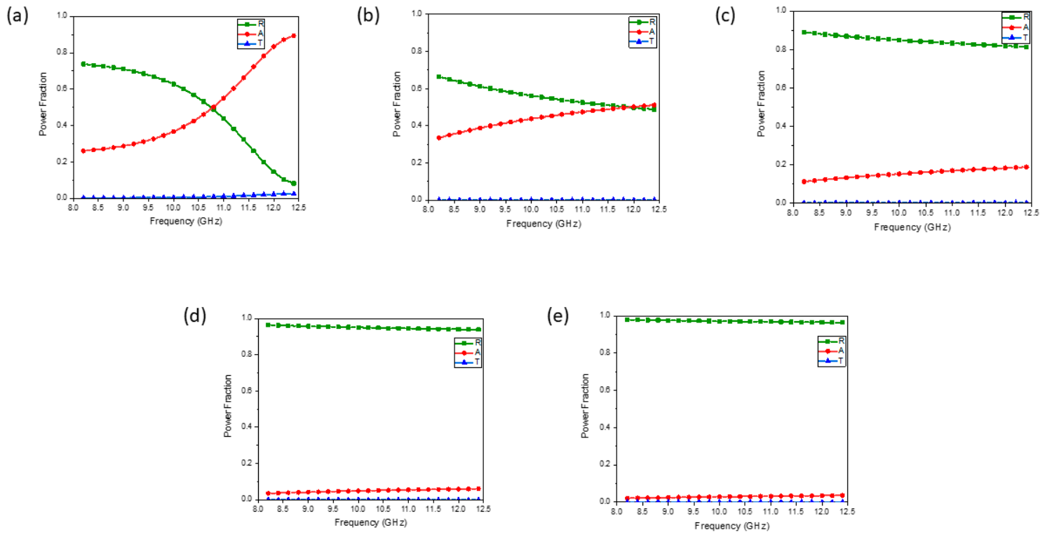
For applications requiring SET in the range 50–100 dB, porous-to-medium graphite felt (σ = 10–50 S/m) at 4–8 mm or medium-density graphite felt (σ = 100 S/m) at 2–4 mm are both viable options [7,19]. The choice between them depends on the weight and volume budget: a 3 mm-thick medium-density felt can achieve equivalent SE to a 7–8 mm-thick low-density felt, but at substantially lower volume. For applications requiring SET in the range 100–150 dB, medium-to-dense graphite (σ = 100–300 S/m) at thicknesses above 3 mm is required, and thickness remains a reliable compensating parameter within this conductivity range [17]. For the most demanding applications requiring SET above 150 dB, dense graphite (σ ≥ 300 S/m) is necessary; at σ ≥ 1000 S/m, the simulated threshold of 194 dB is reached at thicknesses as low as 1 mm. In this high-conductivity regime, the saturation effect means that any additional thickness beyond 3–4 mm contributes no further measurable improvement, and the designer should focus on maximizing conductivity through densification, heat treatment, or the use of pyrolytic graphite [11,12] rather than increasing sample thickness. For all 1100 frequency-domain simulation solutions comprising the full parametric dataset, the energy conservation condition |S11|2 + |S21|2 <= 1 was verified at each frequency point [21]. The absorbed power fraction A = 1 − |S11|2 − |S21|2 was positive in all cases, confirming the physical consistency of all results. Figure 10 illustrates the energy balance for all five conductivity levels at d = 5 mm, providing a comprehensive view of how the dominant shielding mechanism evolves across the full range of conductivities.
Figure 10.
Power balance verification across all five conductivity levels at d = 5 mm. (a) σ = 1 S/m: frequency-dependent crossover from reflection- to absorption-dominant near 11 GHz. (b) σ = 10 S/m: transitional regime with comparable R and A. (c) σ = 100 S/m: reflection-dominant with R = 0.81–0.89. (d) σ = 1000 S/m: strongly reflection-dominant (R > 0.94). (e) σ = 3000 S/m: very strongly reflection-dominant (R > 0.96). T is negligible for σ ≥ 10 S/m.
As Figure 10 shows, the power balance evolves systematically with conductivity. In Figure 10a (σ = 1 S/m), R decreases from ~0.74 at 8.2 GHz to ~0.08 at 12.4 GHz while A increases from ~0.26 to ~0.89, with a crossover near 11 GHz. This strong frequency dependence is consistent with the Fabry–Pérot interference effect. T is small but non-negligible (~0.002–0.025), consistent with the electrically thin regime. In Figure 10b (σ = 10 S/m), R ranges from ~0.67 to ~0.49 and A from ~0.33 to ~0.51 across the X-band, representing a transitional regime in which R and A are comparable, approaching near-equal division at high frequencies. In Figure 10c (σ = 100 S/m), R dominates at 0.81–0.89, with A contributing only 0.11–0.19. In Figure 10d,e (σ = 1000 and 3000 S/m), R is overwhelmingly dominant at 0.94–0.98, with A below 0.06 in both cases and T negligible throughout [5]. The R + T + A = 1 identity is satisfied to within the numerical precision of the solver at every frequency point, providing a rigorous self-consistency check on the simulation results.
At the high-conductivity extreme, σ = 3000 S/m in thin dimensions, the reflected fraction R = |S11|2 approaches 0.97, meaning approximately 97% of the incident power is physically reflected back toward the source, and only ~3% is absorbed. Dense graphite composites, therefore, function primarily as reflective shields in terms of power balance [26]. This has important practical implications: dense graphite shields will reflect most incident EMI back toward the source, potentially creating secondary interference problems in noise-sensitive electronic assemblies [26]. In such cases, porous graphite felt (σ = 1–10 S/m), which absorbs 33–89% of incident power depending on frequency and thickness, is the preferred choice despite its lower absolute SET, as it avoids the near-total reflection (R > 0.96) characteristic of dense graphite [5]. These limiting cases bracket the practical range of graphite shielding behavior and are consistent with published experimental data for comparable materials [7,14,19].
5. Conclusions
This study presented a systematic finite-element investigation of electromagnetic interference (EMI) shielding effectiveness (SE) in graphite-based materials, spanning conductivity values from highly porous graphite (σ = 1 S/m) to dense graphite composites (σ = 3000 S/m). Using a validated COMSOL Multiphysics 5.6 model with the TBC in a WR90 waveguide, the effects of conductivity, thickness, and frequency across the X-band (8.2–12.4 GHz) were examined through 1100 frequency-domain simulations. The results identified conductivity as the dominant design parameter governing shielding performance. Increasing conductivity from 1 to 3000 S/m improved SET by approximately 185 dB at a thickness of 5 mm, demonstrating a substantially greater influence than thickness variation alone. The shielding mechanism was also found to depend strongly on conductivity. Low-conductivity porous graphite (σ = 1–10 S/m) exhibited absorption-dominated behavior, whereas highly conductive graphite (σ ≥ 100 S/m) functioned primarily through reflection despite conventional decomposition methods indicating strong absorption contributions. Conductivity-dependent saturation thicknesses were observed, with SET reaching a plateau at approximately 4–5 mm for σ = 100 S/m and at 1–2 mm for σ ≥ 1000 S/m. In contrast, porous graphite felt (σ = 10 S/m) exhibited continuous, near-linear growth in shielding throughout the investigated thickness range without saturation. Based on these results, a conductivity–thickness design heatmap was developed as a practical engineering tool for selecting material parameters required to achieve target shielding levels. The developed simulation framework closely resembles standard VNA waveguide measurement configurations and therefore provides a useful basis for future experimental validation. Further work should include experimental studies, anisotropic conductivity models, multilayer architectures, extension to higher-frequency bands, and sensitivity analysis of dielectric properties at low conductivity values.
Author Contributions
Conceptualization, M.M. and M.S. (Mohamed Swillam); methodology, M.M.; software, M.S. (Mostafa Sayed); validation, M.M., M.R. and M.S. (Mohamed Swillam); formal analysis, M.S. (Mostafa Sayed); investigation, M.S. (Mostafa Sayed) and M.M.; resources, M.S. (Mostafa Sayed) and M.A.; data curation, M.S. (Mostafa Sayed); writing—original draft preparation, M.S. (Mostafa Sayed); writing—review and editing, M.M. and M.S. (Mohamed Swillam); visualization, M.S. (Mostafa Sayed) and M.R.; supervision, M.M. and M.S.; project administration, M.M.; funding acquisition, M.M. and M.S. (Mohamed Swillam). All authors have read and agreed to the published version of the manuscript.
Funding
This research was supported by The American University in Cairo under the Bartlett Research Grant (Cycle 6), Grant No. Bartlett-Cycle 6-SSE-PSYCH-M.O-.01.
Data Availability Statement
The data supporting the findings of this study are available from the corresponding author upon reasonable request.
Acknowledgments
The authors gratefully acknowledge financial support from the Bartlett Fund for Critical Challenges, at the American University in Cairo, Egypt.
Conflicts of Interest
The authors declare no conflict of interest.
References
- Chung, D.D.L. A perspective on electromagnetic interference shielding materials comprising exfoliated graphite. Carbon 2024, 218, 118569. [Google Scholar] [CrossRef] [Scilit]
- IEC 61000-4-3; Electromagnetic Compatibility (EMC)—Part 4-3: Testing and Measurement Techniques: Radiated, Radio-Frequency, Electromagnetic Field Immunity Test. IEC: Geneva, Switzerland, 2020.
- Paul, C.R. Introduction to Electromagnetic Compatibility, 2nd ed.; Wiley-Interscience: Hoboken, NJ, USA, 2006. [Google Scholar]
- Guan, L.; Fan, J.; Ng, Z.K.; Teo, E.H.T.; Le Ferrand, H. Modulation of the electromagnetic shielding effectiveness through micro/macrostructure design for electronic packaging. NPG Asia Mater. 2024, 16, 54. [Google Scholar] [CrossRef] [Scilit]
- Lee, J.H.; Kim, Y.S.; Ru, H.J.; Lee, S.Y.; Park, S.J. Highly flexible fabrics/epoxy composites with hybrid carbon nanofillers for absorption-dominated electromagnetic interference shielding. Nano-Micro Lett. 2022, 14, 214. [Google Scholar] [CrossRef] [Scilit] [PubMed]
- Zecchi, S.; Cristoforo, G.; Bartoli, M.; Tagliaferro, A.; Torsello, D.; Rosso, C.; Boccaccio, M.; Acerra, F. A comprehensive review of electromagnetic interference shielding composite materials. Micromachines 2024, 15, 187. [Google Scholar] [CrossRef] [Scilit] [PubMed]
- Yin, Z.; Cai, W.; Lu, J.; Yu, B.; Wang, B.; Song, L.; Hu, Y. Cost-effective graphite felt and phosphorous flame retardant with extremely high electromagnetic shielding. Compos. Part B Eng. 2022, 236, 109819. [Google Scholar] [CrossRef] [Scilit]
- Pierson, H.O. Handbook of Carbon, Graphite, Diamond and Fullerenes: Properties, Processing and Applications; Noyes Publications: Park Ridge, NJ, USA, 1993. [Google Scholar]
- Ali, M.S.; Yegireddy, H.; Rao, Y.K.S.S.; Sahu, N.C.; Kolla, N.K.; Syed, J. Enhanced electromagnetic shielding in X-band applications using graphene and multiwalled carbon nanotube reinforced epoxy nanocomposites. J. Mater. Eng. Perform. 2025, 35, 19955–19964. [Google Scholar] [CrossRef] [Scilit]
- Dresselhaus, M.S.; Dresselhaus, G.; Sugihara, K.; Spain, I.L.; Goldberg, H.A. Graphite Fibers and Filaments; Springer: Berlin/Heidelberg, Germany, 1988. [Google Scholar]
- Taş, M.; Elden, G. The effects of heat treatment on the felt electrodes in vanadium redox flow battery. In Proceedings of the 5th International Symposium on Materials for Energy Storage and Conversion (mESC-IS 2021), Online, 11–17 September 2021. [Google Scholar]
- Melke, J.; Jakes, P.; Langner, J.; Riekehr, L.; Kunz, U.; Zhao-Karger, Z.; Nefedov, A.; Sezen, H.; Wöll, C.; Ehrenberg, H.; et al. Carbon materials for the positive electrode in all-vanadium redox flow batteries. Carbon 2014, 78, 220–230. [Google Scholar] [CrossRef] [Scilit]
- Celzard, A.; Marêché, J.F.; Furdin, G. Modelling of exfoliated graphite. Prog. Mater. Sci. 2005, 50, 93–179. [Google Scholar] [CrossRef] [Scilit]
- Wilson, N.H.; Anju; Masař, M.; Machovský, M.; Škoda, D.; Urbánek, P.; Urbánek, M.; Pöschl, M.; Vilčáková, J.; Kuřitka, I.; et al. Excellent electromagnetic interference shielding of multi-layered thermoplastic polyurethane nanocomposites with CoFe2O4 nanoparticles and graphite. Adv. Compos. Hybrid Mater. 2025, 8, 101. [Google Scholar] [CrossRef] [Scilit]
- Kunkel, G.M. Shielding of Electromagnetic Waves: Theory and Practice; Springer: Cham, Switzerland, 2019. [Google Scholar] [CrossRef] [Scilit]
- Schelkunoff, S.A. Electromagnetic Waves; Van Nostrand: New York, NY, USA, 1943. [Google Scholar]
- Sarto, M.S.; Tamburrano, A. Innovative test method for the shielding effectiveness measurement of conductive thin films in a wide frequency range. IEEE Trans. Electromagn. Compat. 2006, 48, 331–341. [Google Scholar] [CrossRef]
- Pozar, D.M. Microwave Engineering, 4th ed.; John Wiley & Sons: Hoboken, NJ, USA, 2012. [Google Scholar]
- Park, J.; Kwac, L.K.; Kim, H.G.; Shin, H.K. Fabrication and characterization of waste wood cellulose fiber/graphene nanoplatelet carbon papers for application as electromagnetic interference shielding materials. Nanomaterials 2021, 11, 2878. [Google Scholar] [CrossRef] [Scilit] [PubMed]
- Holloway, C.L.; Kuester, E.F. Power loss associated with conducting and superconducting rough interfaces. IEEE Trans. Microw. Theory Tech. 2000, 48, 1601–1610. [Google Scholar] [CrossRef] [Scilit]
- COMSOL Inc. COMSOL Multiphysics Programming Reference Manual; COMSOL: Burlington, MA, USA, 2020; Available online: https://www.comsol.com (accessed on 1 January 2024).
- Senior, T.B.A.; Volakis, J.L. Approximate Boundary Conditions in Electromagnetics; IEE: London, UK, 1995. [Google Scholar]
- Rodríguez, F.; Meneses, M.; Chiné, B. Computational analysis of metal foams for EMI shielding using COMSOL Multiphysics. In Proceedings of the COMSOL Conference 2019, Cambridge, UK, 2–4 October 2019. [Google Scholar]
- Blachowicz, T.; Wójcik, D.; Surma, M.; Magnuski, M.; Ehrmann, G.; Ehrmann, A. Textile fabrics as electromagnetic shielding materials—A review of preparation and performance. Fibers 2023, 11, 29. [Google Scholar] [CrossRef] [Scilit]
- Manogaran, R.; Murugesan, M. A review on recent advancements in textile fabrics for electromagnetic interference (EMI) shielding materials. Mater. Today Commun. 2025, 43, 111879. [Google Scholar] [CrossRef] [Scilit]
- Isari, A.A.; Ghaffarkhah, A.; Hashemi, S.A.; Wuttke, S.; Arjmand, M. Structural design for EMI shielding: From underlying mechanisms to common pitfalls. Adv. Mater. 2024, 36, 2310683. [Google Scholar] [CrossRef] [Scilit] [PubMed]
- Karlsson, A. Approximate boundary conditions for thin structures. IEEE Trans. Antennas Propag. 2009, 57, 144–148. [Google Scholar] [CrossRef] [Scilit]
- Moučka, R.; Goňa, S.; Sedlačík, M. Accurate measurement of the true plane-wave shielding effectiveness of thick polymer composite materials via rectangular waveguides. Polymers 2019, 11, 1603. [Google Scholar] [CrossRef] [Scilit] [PubMed]

Disclaimer/Publisher’s Note: The statements, opinions and data contained in all publications are solely those of the individual author(s) and contributor(s) and not of MDPI and/or the editor(s). MDPI and/or the editor(s) disclaim responsibility for any injury to people or property resulting from any ideas, methods, instructions or products referred to in the content. |
© 2026 by the authors. Licensee MDPI, Basel, Switzerland. This article is an open access article distributed under the terms and conditions of the Creative Commons Attribution (CC BY) license.