


Abstract
GaN-on-sapphire structure is currently playing an important role in developing modern optoelectronic and electronic devices. Cross-sectional Raman scattering (RS) measurements were conducted along the growth direction of GaN-on-sapphire structures; the 4.0 μm R4 and 7.6 μm N7 layers were measured using step intervals of 0.5 μm and 1.0 μm, respectively. Characterization techniques, such as scanning electron microscopy, optical transmission and spectroscopic ellipsometry, have been applied to these GaN/sapphire structures and provide information on the crystalline properties of the two GaN films. Cross-sectional Raman measurements showed sample-dependent shifts in the fitted GaN E2(high) and E1(LO) peak positions. The fitted E2(high) peak positions were used to estimate the relative stress profiles, while spatial correlation model analysis provided model-dependent estimates of the effective phonon correlation lengths and damping constants. Longitudinal optical phonon–plasmon coupling fitting of the E1(LO) modes was used to estimate the carrier concentration and mobility. The distinctive findings may enhance the comprehension of GaN/sapphire and present valuable benchmarks for others within this field.
1. Introduction
Gallium Nitride (GaN) growth on sapphire has been studied since the late 1960s, beginning with Melton and Pankove [1]. Nakamura et al. demonstrated blue laser diodes based on a GaN-on-sapphire structure [2]. Amano presented a Nobel Lecture with an overview of historical breakthroughs for successful MOVPE of GaN on sapphire and p-type doping [3]. Gao et al. reviewed recent advances in III-nitride flexible optoelectronics, from materials to applications [4]. GaN/sapphire structures have been used in a wide range of electronic and optoelectronic devices [5]. Recent MOCVD studies have demonstrated high-efficiency InGaN-based green LEDs and high-power AlGaN-based deep-UV LEDs on sapphire-related structures [6,7]. Raman scattering is an established non-destructive method for characterizing GaN and related materials [8]. Previous studies have examined cross-sectional Raman spectra [9], structural and optical properties [10], and anisotropic strain using polarized Raman spectroscopy [11]. Nootz et al. [12] correlated spatially resolved Raman shifts with dislocation density, whereas Chaldyshev et al. [13] investigated laterally epitaxially overgrown GaN/sapphire. Duan et al. [14] combined Raman spectroscopy with HRXRD to characterize GaN grown on sapphire and 4H-SiC, while Belyaev et al. [15] used confocal Raman microscopy to profile strain and carrier concentration in a cleaved GaN Gunn-diode structure. Additional optical properties of GaN-based structures have also been reported [16]. These studies demonstrate that Raman-based stress and carrier analyses are established methods, while the sample structures, measurement configurations, and complementary characterization methods differ from those used in the present work. Recent GaN/sapphire studies have also addressed photonic and power devices, leakage mechanisms, acoustic structures, sensors, carrier transport, and temperature-dependent optical properties [17,18,19,20,21,22,23,24].
In this work, cross-sectional Raman spectroscopy is used to compare two MOCVD-grown GaN/sapphire samples with GaN layer thicknesses of 7.6 and 4.0 μm. SEM, OT, and SE were used to provide complementary structural and optical information. First, two GaN-on-sapphire samples with various GaN film thicknesses were characterized by cross-section scanning electron microscopy (SEM), optical transmission (OT) and spectroscopic ellipsometry (SE), providing complementary structural and optical characterization. Second, cross-section Raman scattering revealed the GaN E2(high) and E1(LO) band shift, indicating the variation of the compressive stress along the film growth direction. The results from this investigation could expand the understanding of the investigated GaN/sapphire structures and provide useful references for this field.
2. GaN-on-Sapphire Samples
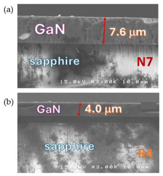
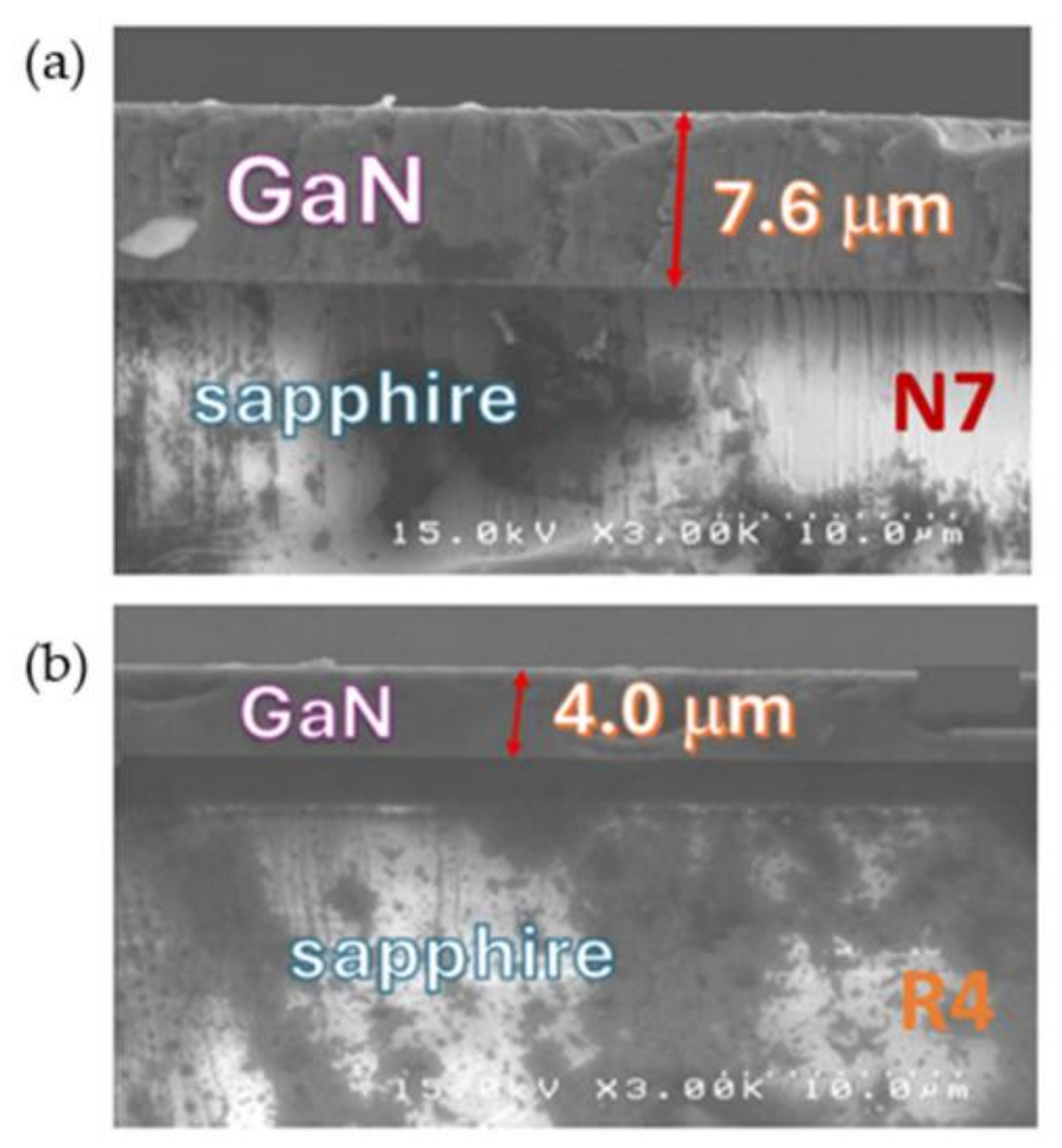
GaN films were grown on c-sapphire by metal-organic chemical vapor deposition (MOCVD) under low-pressure conditions (10-250 Torr), with trimethylgallium (TMGa, Ga(CH3)3) and ammonia (NH3) as gallium and nitrogen sources, respectively, plus with hydrogen (H2) acting as the carrier gas. The growth process began with the formation of ~200 Å GaN buffer layer at ~530 °C, followed by increasing the substrate temperature to ~1040 °C for the deposition of the main GaN layer [10]. Low-temperature GaN nucleation layers grown on sapphire are known to exhibit growth- and annealing-dependent changes in surface morphology, crystalline phase, and optical properties [25]. Related MOVPE studies of GaN heteroepitaxy have also shown that AlGaN interlayers can modify the strain state, while SiN masking can contribute to threading-dislocation reduction during subsequent GaN growth [26]. Two GaN-on-sapphire samples, N7 and R4, with their original run numbers of n7600 and r4056, respectively, are studied in this work. GaN film thicknesses were determined to be 7.6 μm for N7 and 4.0 μm for R4 from cross-sectional imaging using a field-emission scanning electron microscope (JEOL JSM-7000F, Center for Condensed Matter Sciences, National Taiwan University, Taipei, Taiwan and the manufacturer JEOL was located in Akishima, Tokyo, Japan.) (FESEM, Sigma500/VP, ZEISS), as shown in Figure 1. N7 and R4 were selected as representative GaN/sapphire samples with different GaN layer thicknesses and well-defined cross-sections suitable for Raman line scanning.
Figure 1.
Cross-section scanning electron microscopy (SEM) patterns for two GaN-on-sapphire samples of (a) N7 with d (GaN) = 7.6 μm and (b) R4 with d (GaN) = 4.0 μm, respectively.
GaN growth on sapphire generally evolves from a low-temperature nucleation or buffer layer through an initial three-dimensional growth and coalescence stage to a smoother two-dimensional high-temperature GaN layer [1,3,25]. These growth stages may differ in strain relaxation, defect evolution, and impurity incorporation. Because the individual regions were not independently identified in the present samples, this growth sequence is used only as a qualitative framework for interpreting the depth-dependent results rather than for assigning discrete layer boundaries.
For the present samples, OT records the integrated optical response of the complete GaN/sapphire structure and may include contributions from the thin buffer and interfacial regions. SE mainly provides model-derived thickness, surface roughness, and optical constants for the dominant GaN layer. Cross-sectional Raman spectroscopy probes micrometer-scale variations within the main GaN layer, but the present sampling intervals are insufficient to isolate the approximately 200 Å buffer layer or to identify a sharp boundary between the three-dimensional and two-dimensional growth regions. Measurements near and beyond the nominal GaN/sapphire interface were retained for completeness. Because these spectra may contain contributions from both GaN and sapphire owing to spatial averaging, no layer-specific stress interpretation is assigned to these points.
3. Analysis and Discussion of Measurement Results
3.1. OT Measurements
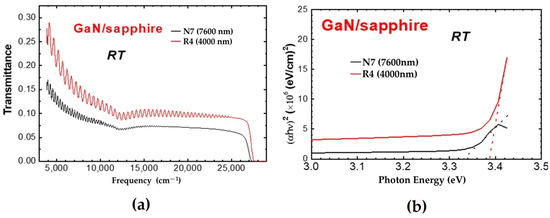
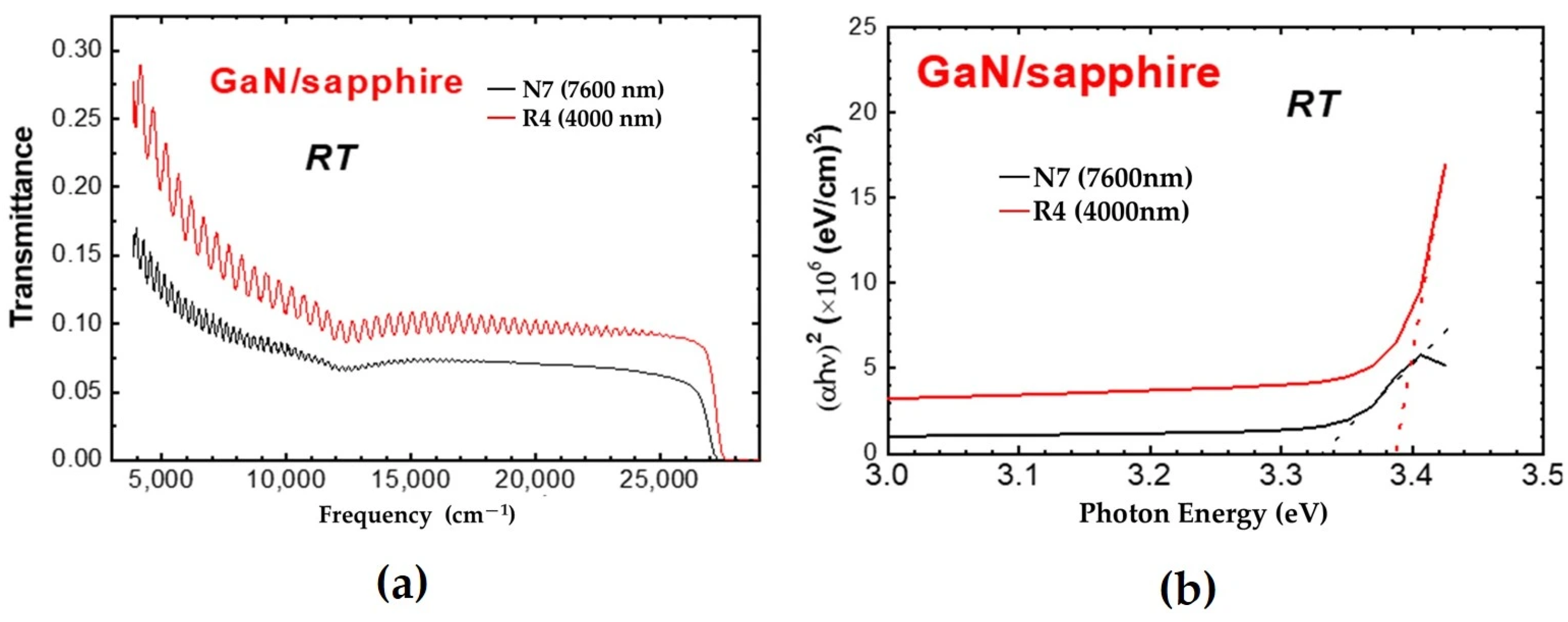
Room-temperature (RT) UV–visible OT spectra of GaN-on-sapphire samples were measured by a UV–visible spectrophotometer (OmniAs, Zolix). The instrument provided a spectral resolution of 0.1 nm and an accuracy of approximately 0.3%. Figure 2a shows the OT spectra of N7 and R4 over 3000–29,000 cm−1, corresponding to wavelengths of 345–3300 nm and photon energies of 0.38–3.59 eV. The periodic oscillations in the figure are due to multiple reflections between the air–GaN and GaN–substrate interfaces [27].
Figure 2.
(a) OT spectra in frequency range of 3000–29,000 (cm−1) and (b) relations of (αhν)2 versus photon energy (eV) in energy range of 3.0–3.5 eV of two GaN-on-sapphire samples of N7 and R4, respectively.
For the present comparative analysis, the apparent absorption coefficient (α) was estimated from the measured transmittance (T) using the following simplified Beer–Lambert-type relation:
where t is the GaN layer thickness obtained from the cross-sectional SEM measurements shown in Figure 1. Because this simplified relation does not explicitly correct for reflection losses or thin-film interference, α is treated as an apparent absorption coefficient for comparative analysis. Further, the relationship between the absorption coefficient (α) and photon energy (hν in eV) can be described by the Tauc empirical relation [27,28]
where C is a constant. Figure 2b shows the corresponding relations of (αhν)2 versus photon energy (eV) for the two GaN films, from which, through extrapolating the linear part of the (αhν)2~eV curve to reach the X-axis, the band gap energy Eg (GaN) can be obtained, i.e., using the Tauc method [28]. Figure 2b shows the Eg (GaN) values to be 3.34 eV for N7 and 3.39 eV for R4. Both values are slightly less than the stress-free Eg (GaN) value of ~3.42 eV [2,4].
Optical transmission records the through-thickness optical response of the complete GaN/sapphire structure and therefore complements the model-based SE analysis. The observed differences may contain contributions from the GaN layer, buffer region, and interfaces. However, no layer-specific assignment is made from the present OT measurements.
3.2. Spectroscopic Ellipsometry (SE) Measurements
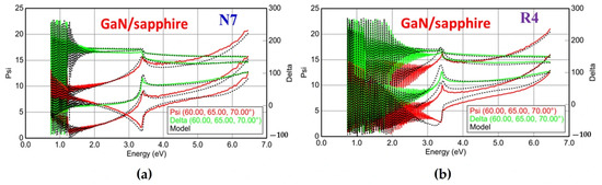
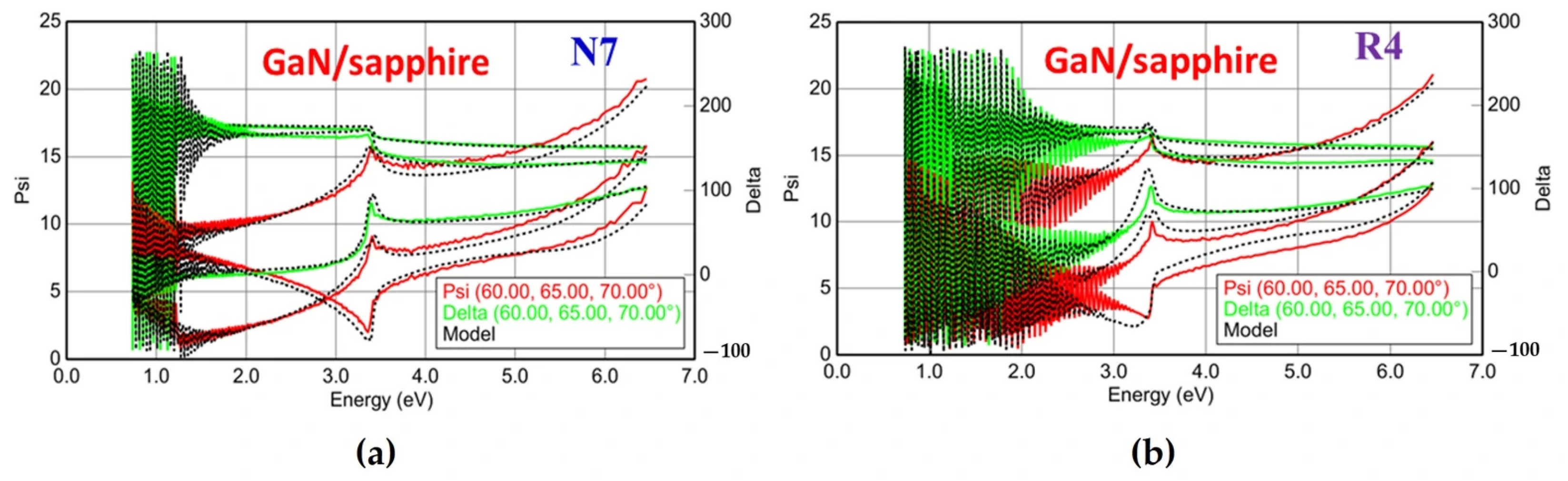
A dual-rotation compensation Mueller matrix ellipsometer (ME-L model, Wuhan Eoptics Technology Co., Ltd., Wuhan, China) was used at room temperature to measure SE spectra at three incidence angles of 60°, 65°, and 70°. The spectra were fitted using CompleteEASE software (Version: 5.29) (J. A. Woollam Co., USA), and the fitted quantities included the GaN thickness, surface roughness, and optical constants. Figure 3 displays the typical RT spectroscopic ellipsometry (SE) spectra measured at incidence angles of 60°, 65°, and 70° and in the energy range of 0.75–6.4 eV of GaN-on-sapphire samples for (a) N7 and (b) R4, respectively. Fitting with CompleteEASE yielded GaN film thicknesses of 7.90 μm for N7 and 4.28 μm for R4, together with surface roughness values of 21 nm and 35 nm, respectively. The SE-determined GaN film thicknesses are approximately 4% and 7% higher than those determined from the cross-sectional SEM measurements for N7 and R4, respectively. These slight differences may have arisen from different measurements at different spots of the samples.
Figure 3.
RT spectroscopic ellipsometry (SE) spectra with incident angles of 60°, 65° and 70°, in the energy range of 0.75–6.4 eV of GaN-on-sapphire samples for (a) N7 and (b) R4, respectively.
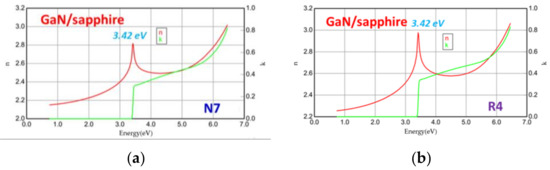
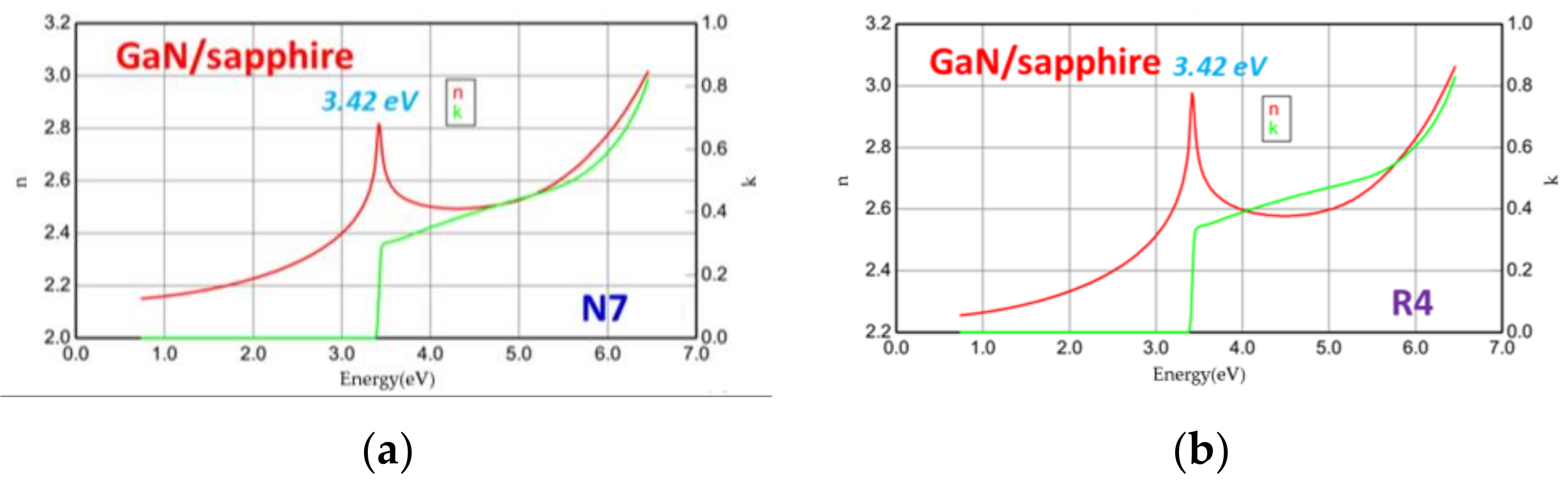
The optical parameters of refractive index n, extinction coefficient k and optical absorption α, as well as their dependence on energy (eV), can be deduced from measured SE spectra. Figure 4 presents the RT SE spectral-deduced relationships of n~eV and k~eV in 1.0–6.5 eV for GaN-on-sapphire samples of (a) N7 and (b) R4, respectively. They show the n~eV curves with maxima peaks at about 3.42 eV and the k~eV curves having the change near the absorption edge with the midpoints near 3.42 eV also, and both are close to the Eg (GaN).
Figure 4.
RT SE spectra-deduced relationships of refractive index n vs. eV (red) and extinction coefficient k vs. eV (green) in the energy range of 0.75–6.45 eV of GaN-on-sapphire samples for (a) N7 and (b) R4, respectively.
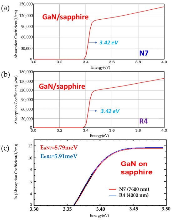
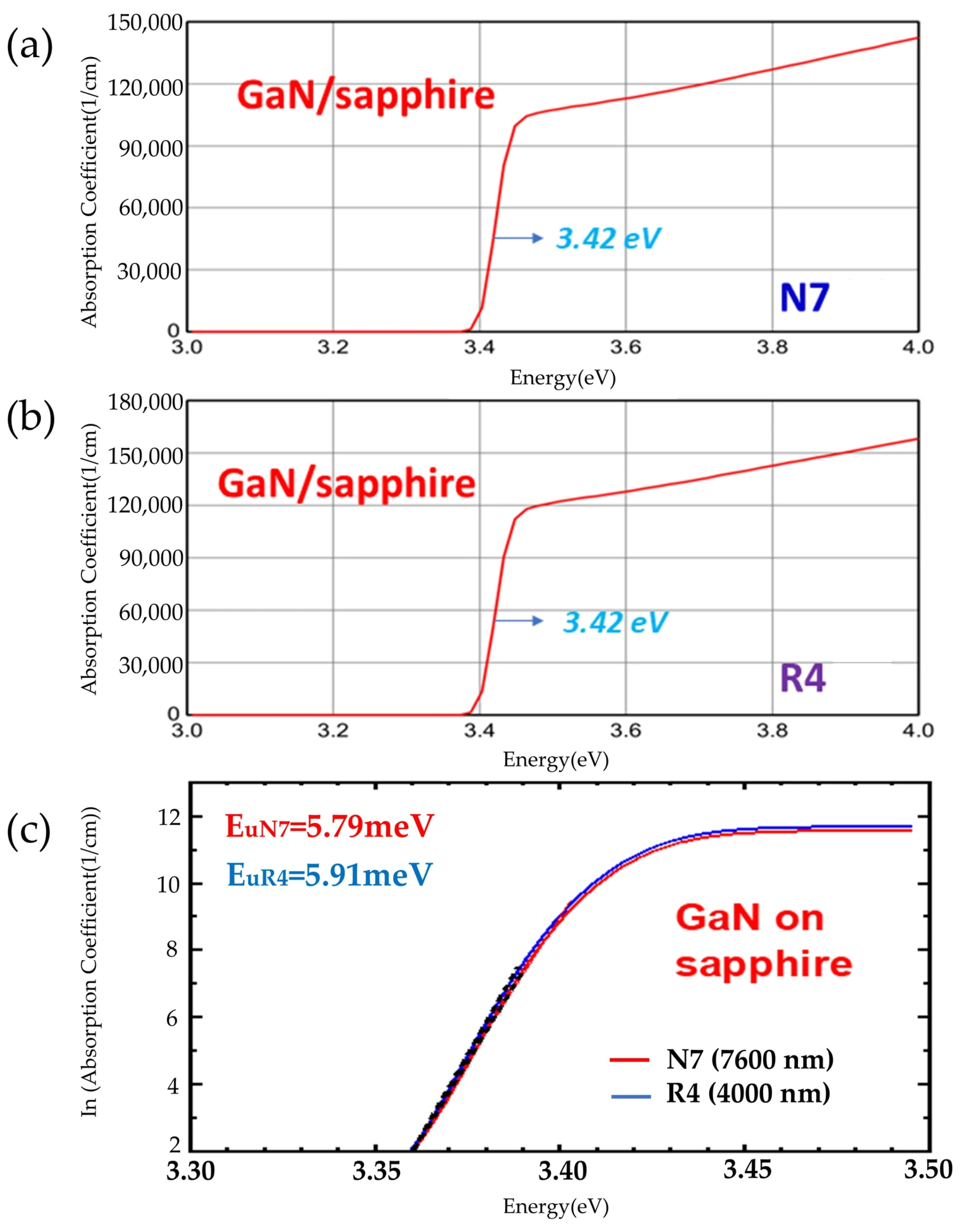
Figure 5 shows the RT SE spectral-deduced relationships of α~eV in 3.0–4.0 eV for GaN/sapphire samples of (a) N7 and (b) R4, respectively. They show the α~eV curves having sharp absorption edge between 3.40–3.45 eV, like the k~eV curves in Figure 4, due to α = 4πk/λ.
Figure 5.
RT SE-deduced relationships of absorption coefficient α~eV in 3.0–4.0 eV of GaN-on-sapphire (a) N7 and (b) R4, respectively. (c) Deduced ln(α)~eV in 3.30–3.50 eV of GaN/sapphire N7 and R4.
Below approximately 3.405 eV, the absorption-coefficient spectra exhibit exponential tails attributed to structural disorder and electron–phonon interactions. These Urbach tails are described by Equation (3) [29].
where the Urbach energy EU is acquired from the inverse slope of the derivative of ln(α) with respect to photon energy (eV). Because the detailed dielectric-function parameterization, surface-layer model, and near-band-edge fitting residuals are not available for the present analysis, the SE-derived absorption coefficient and Urbach energy are treated as model-dependent quantities. The reported Urbach energies are therefore used only for comparison between N7 and R4.
Figure 5c exhibits the SE-deduced ln(α) versus photon energy relationships for N7 and R4. The apparent Urbach energies obtained from the linear region are 5.79 meV for N7 and 5.91 meV for R4. These values are lower than the value of approximately 18 meV reported for GaN/Si [29].
Piccardo et al. reported the Urbach tails in semiconductors being commonly linked to disorder in composition and noted the GaN’s EU of about 12–15 meV [30]. S. Chichibu et al. obtained the temperature-dependent Urbach energy in a wurtzite GaN epilayer, which varied from 12 meV at 300 K down to 6.3 meV at 80 K [31]. Finn et al. reported Urbach energies in the range of 11–13 meV for Al0.48Ga0.52N/Al0.63Ga0.37N structures [32]. Ugur et al. reviewed Life on the Urbach Edge and listed more EU values of semiconductors, PV materials and Perovskites, with EU = 7.5 meV for GaAs and 9.4 meV for InP, and all others beyond 10 meV [33]. Ledinsky et al. reported that methylammonium lead iodide (CH3NH3PbI3) exhibits lower Urbach energy in comparison with conventional crystalline semiconductors, such as Si, GaAs, InP and GaN [34].
3.3. Cross-Section Raman Measurements and Stress Distribution
Cross-sectional micro-Raman measurements were performed at room temperature in a backscattering configuration using a 532 nm diode laser and a SENTERRA spectrometer. The instrument incorporates the Sure_Cal automatic continuous-calibration system, which records the laser excitation line and neon-lamp emission lines with each spectrum to correct changes in the laser and spectrograph. The manufacturer-specified wavenumber accuracy and precision of the calibrated Raman-shift axis are better than 0.1 cm−1. Each sample was mounted vertically in the narrow slot of a clamp and scanned from the GaN surface toward the sapphire substrate, with nominal sampling intervals of 1.0 μm for N7 and 0.5 μm for R4. These intervals represent the spacing between adjacent measurement positions rather than the effective spatial resolution. Spectra were examined over 500–770 cm−1. The E2(high) peaks were fitted with a Gaussian function over 564–572 cm−1 for N7 and 567–572 cm−1 for R4, while the E1(LO) regions analyzed were 730–750 cm−1 for N7 and 736–752 cm−1 for R4. The specified wavenumber accuracy is distinct from the spectral resolution, which depends on the optical configuration. Since the archived records do not provide the complete optical and acquisition settings—including the grating, slit or pinhole, objective, laser power at the sample, acquisition time, accumulation number, and repeated-scan information—the configuration-specific spectral and effective spatial resolutions and experimental error bars cannot be reliably determined for this dataset. Peak positions are therefore presented as fitted values, and spectra near the nominal GaN/sapphire interface are interpreted cautiously because the finite probe volume may sample both materials.
The fitted E2(high) peak positions were used to estimate relative stress trends along the GaN growth direction. The spatial correlation model (SCM) was applied to obtain effective phonon correlation lengths and damping parameters, while longitudinal optical phonon–plasmon coupling (LOPC) fits to the E1(LO) mode were used to estimate carrier concentration and mobility. These quantities are treated as model-dependent parameters for comparing N7 and R4 rather than as independently calibrated measurements.
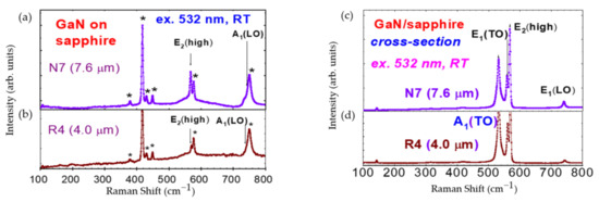
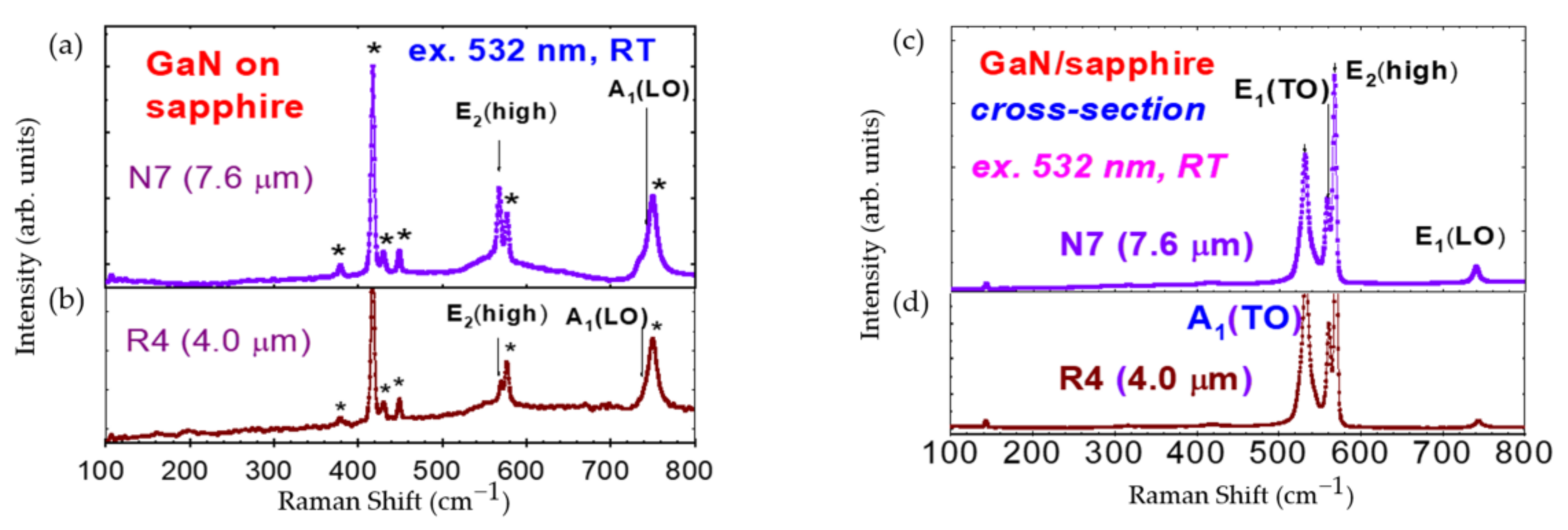
Figure 6a,b present Raman spectra (ex. 532 nm, RT) in a standard backscattering geometry for GaN/sapphire N7 and R4, with dominant contributions from sapphire substrate, marked with *, displaying four peaks in 370–450 cm−1, plus peaks near 578 cm−1 and 754 cm−1 [9]. The GaN E2(high) phonon at ~568 cm−1 in sample N7 is much stronger than the thinner samples in R4. Additionally, GaN A1(LO) mode is detected at the lower-frequency wing of the sapphire-related peak near 754 cm−1 [9].
Figure 6.
Raman spectra (ex. 532nm, RT) in normal backscattering configuration of GaN/sapphire (a) N7 and (b) R4, and at the GaN film cross-section (c) N7 and (d) R4, respectively. Marks * indicate Raman features from sapphire (Al2O3) crystal.
Figure 6c,d exhibit cross-section Raman spectra of these two GaN/sapphire samples, with the laser probe focusing on the GaN film region vertically, away from the sapphire substrate, and showing only Raman signals from crystalline GaN, without sapphire features and with GaN E2(high) at ~568 cm−1 strongly. Two GaN A1(TO) at 531 cm−1 and E1(TO) at 559 cm−1 are observed to be relatively strong, which are forbidden along the c-plane GaN but allowed at the surface perpendicular to the c-axis of GaN [9,11].
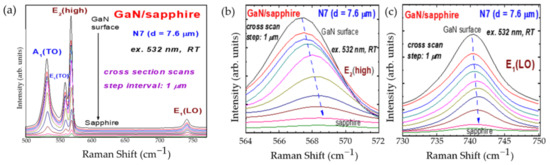
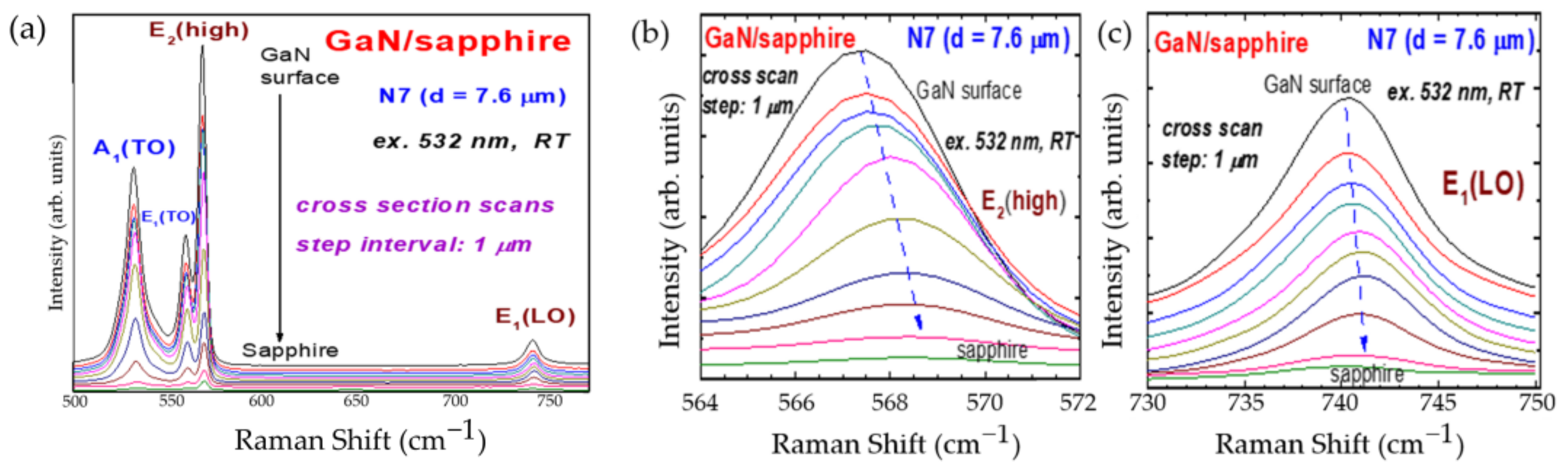
Scanning Raman scattering measurements have been performed along the GaN film cross-section. Figure 7 shows that from the top spectral curve at the GaN surface, downwards to 8 μm away from the surface, and entering sapphire substrate area, the GaN peaks are weak and disappear afterwards. Both E2(high) and E1(LO) peak frequencies increase slightly from the GaN surface towards the GaN/sapphire interface.
Figure 7.
Scanning cross-section multiple Raman spectra (ex. 532 nm, RT) of GaN/sapphire N7 (d = 7.6 μm) with a step interval of 1 μm from the GaN surface into the sapphire substrate: (a) in 500–770 cm−1, showing GaN phonon modes of A1(TO) at ~531 cm−1, E1(TO) at ~559 cm−1, E2(high) at ~568 cm−1 and E1(LO) at 741 cm−1; (b) E2(high) within 564–572 cm−1, and (c) E1(LO) within 730–750 cm−1, respectively.
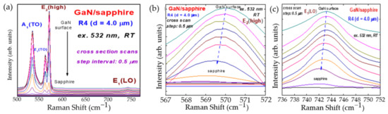
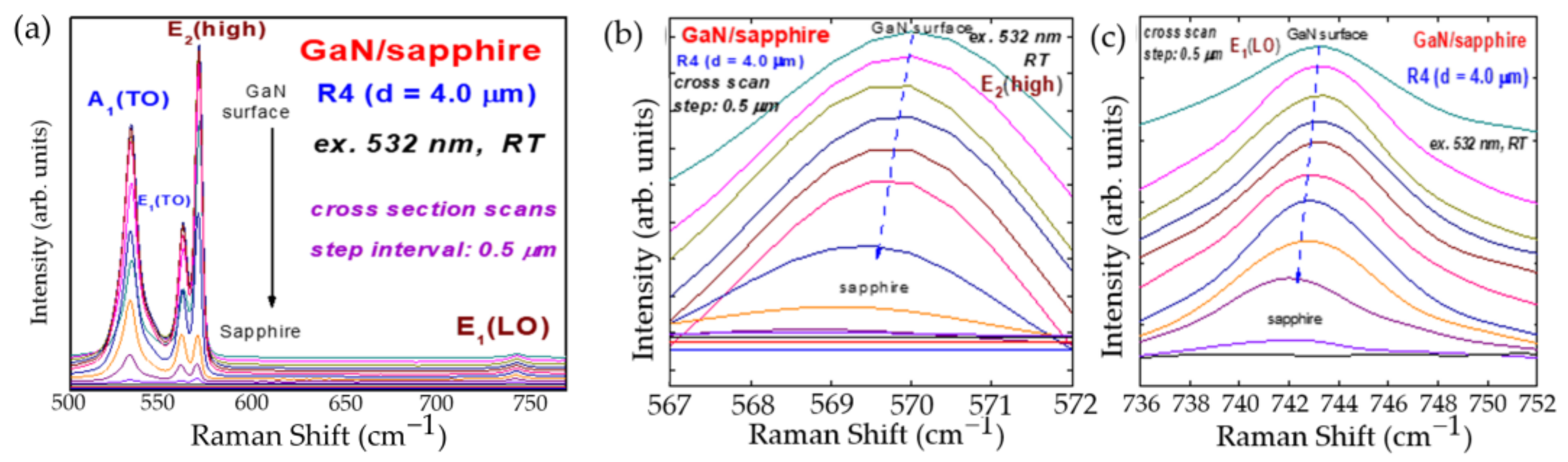
Figure 8 shows that the peak frequencies of these phonon modes again vary slightly along the GaN film cross-section between the GaN surface and the sapphire substrate. It shows that from the top spectra curve at the GaN surface, downwards to the 9th measurement, i.e., at 4.5 μm away from the surface, and entering the sapphire substrate area, the GaN peaks are weak and disappear after the 10th measurement. The trend is reversed in the case of the N7 (d = 7.6 μm) thick film: both E2(high) and E1(LO) peak frequencies decrease from the GaN surface towards the GaN/sapphire interface.
Figure 8.
Scanning cross-section multiple Raman spectra (ex. 532 nm, RT) of GaN/sapphire sample R4 (d = 4.0 μm) with a step interval of 0.5 μm from GaN surface into sapphire substrate: (a) in Raman shift range of 500–770 cm−1, showing GaN phonon modes of A1(TO), E1(TO), E2(high) and E1(LO); (b) E2(high) spectral region of 567–572 cm−1, and (c) E1(LO) spectral area of 736–752 cm−1, respectively.
The shift of the GaN E2(high) phonon mode can be used to estimate the relative biaxial stress in heteroepitaxial GaN [8,14,35]. The Raman frequency difference Δω relative to the stress-free E2(high) frequency of 567.5 cm−1 was used to estimate the GaN layer stress σ using Equation (4).
where K = 4.2 cm−1 GPa−1 is the conversion factor of GaN Raman biaxial stress. The E2(high) peak positions in Figure 7b and Figure 8b were obtained by Gaussian fitting and are listed in Table 1 and Table 2 for samples N7 (7.6 μm) and R4 (4.0 μm), respectively.
Table 1.
Gaussian-fitted E2(high) peak frequencies and estimated stress for GaN/sapphire sample N7 (7.6 μm).
Table 2.
Gaussian-fitted E2(high) peak frequencies and estimated stress for GaN/sapphire sample R4 (4.0 μm).
The residual stress in GaN-on-sapphire may arise from both lattice mismatch during epitaxial growth and the difference in thermal expansion coefficients between GaN and sapphire during cooling. However, the present comparison does not isolate film thickness from other sample-specific growth conditions. Because only two samples are compared and their growth conditions were not independently controlled, the different stress profiles of N7 and R4 cannot be assigned solely to GaN layer thickness. The wurtzite GaN belongs to the hexagonal P63mc space group with lattice constants of ag = 0.3189 nm and cg = 0.5185 nm, while the substrate sapphire (Al2O3) belongs to the trigonal Rc space group with as = 0.4578 nm and cs = 1.2991 nm. There is also a difference between the thermal expansion coefficients of the two materials, 7.50 × 10⁻⁶ K−1 for sapphire and 5.45 × 10⁻⁶ K−1 for GaN. Lattice mismatch and thermal-expansion mismatch may both contribute to the residual biaxial stress in the GaN layer after cooling from the growth temperature. It has been pointed out that large biaxial stress may cause microcracks and degrade the optoelectronic properties of the epitaxial GaN layer [14,35].
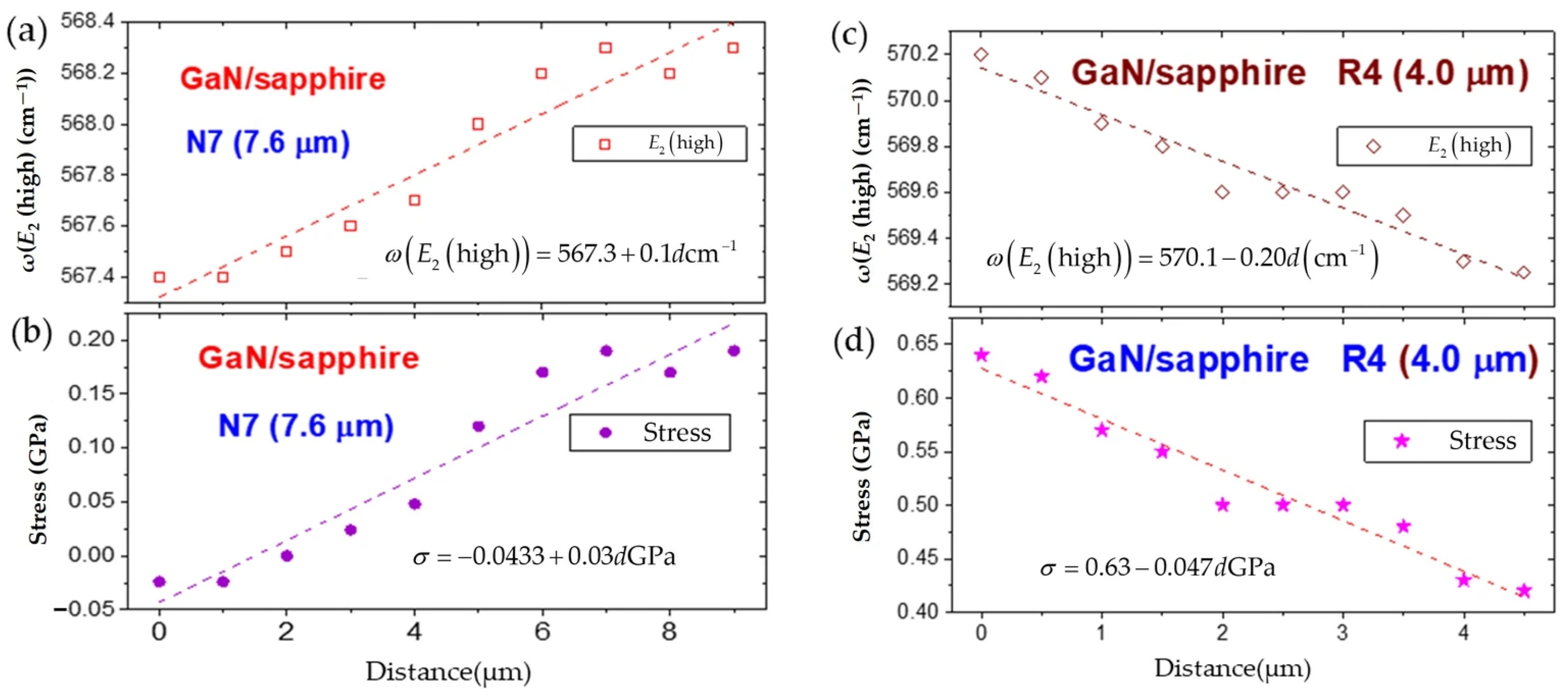
Figure 7b and Figure 8b, together with Table 1 and Table 2, show different overall fitted E2(high) peak-position profiles for N7 and R4. Because independent external verification and scan-specific repeatability data are unavailable, the individual point-to-point stress values are used only to describe the ranges calculated using Equation (4) rather than to identify quantitatively resolved local tensile-to-compressive transitions. For N7, the fitted E2(high) peak positions range from 567.4 to 568.3 cm−1, corresponding to calculated stress estimates from −0.024 to 0.19 GPa. For R4, the fitted peak positions range from 569.25 to 570.2 cm−1, corresponding to stress estimates from 0.43 to 0.64 GPa. These ranges summarize the values calculated using Equation (4) and should not be interpreted as independently determined uncertainty intervals.
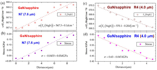
Figure 9 plots the fitted E2(high) positions and corresponding stress estimates against nominal scan distance. Within the nominal GaN regions (0–7 μm for N7 and 0–4 μm for R4), the fitted peak position changes by approximately +0.90 cm−1 for N7 and −0.90 cm−1 for R4. This check does not include peak-fitting variability, signal-to-noise changes, focusing or spatial-averaging effects, or scan-to-scan repeatability. It therefore supports only the directions of the overall fitted profiles, not smaller point-to-point differences of approximately 0.05–0.30 cm−1 or apparent slope changes. The dashed lines are empirical guides. Because Ref. [13] examined laterally overgrown GaN/sapphire under different excitation and sampling conditions, its depth-dependent shifts are not directly comparable with the present data. Ref. [14] combined Raman measurements with HRXRD, whereas the present study lacks an independent structural measurement; therefore, the stress values reported here are treated as Raman-derived estimates.
Figure 9.
Fitted E2(high) peak positions for (a) N7 and (c) R4 and the corresponding stress estimates for (b) N7 and (d) R4 as functions of the nominal scan distance. The dashed lines are empirical guides to the overall profiles.
3.4. Cross-Section Raman E2(High) Mode SCM Fits
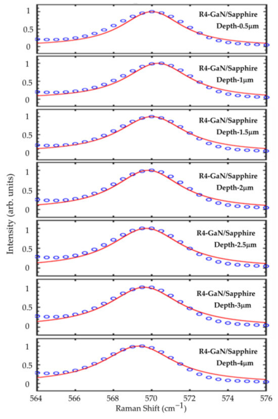
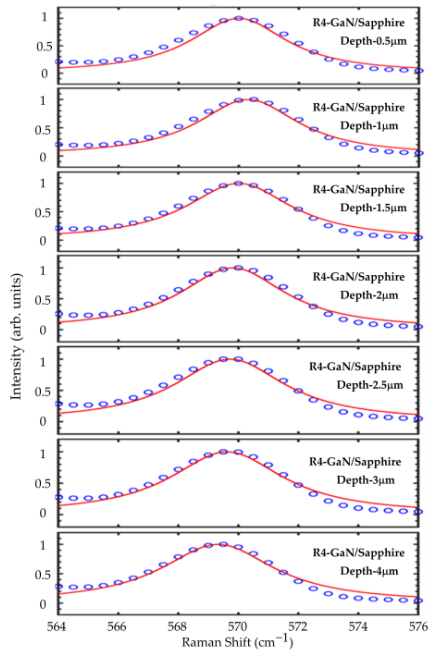
The spatial correlation model (SCM) was applied to the GaN E2(high) mode using Equations (5) and (6) to obtain the effective phonon correlation length and intrinsic linewidth along the growth direction, as shown in Figure 10, Figure 11 and Figure 12 and Table 3 and Table 4 [8,9,36]. Conventional Hall measurements provide layer-averaged transport properties and do not directly resolve micrometer-scale variations along an exposed cross-section. Cross-sectional Raman spectroscopy provides spatially dependent, model-derived information that is complementary to Hall measurements.
Figure 10.
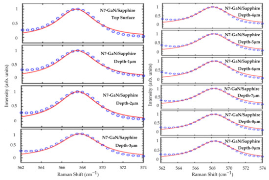
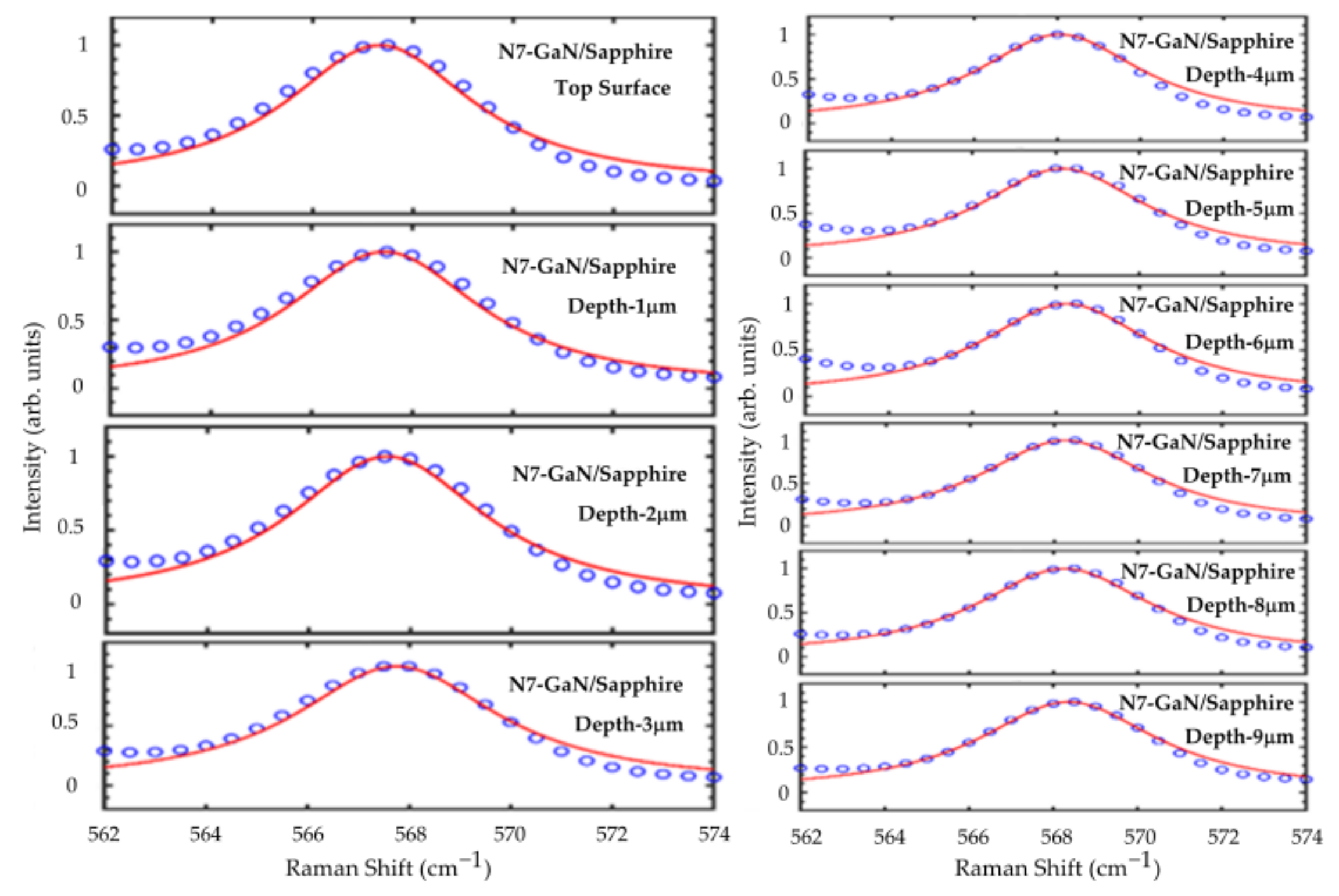
SCM fitting results for ten GaN E2(high) spectra of GaN/sapphire sample N7 (7.6 μm). Experimental data are shown as blue open symbols, and fitted curves are shown as red lines.
Figure 11.
SCM model fitting results of seven GaN E2(high) modes for GaN/sapphire R4 (4.0 μm) with experimental data in blue open symbols from Figure 8b and fitting results in red lines.
Figure 12.
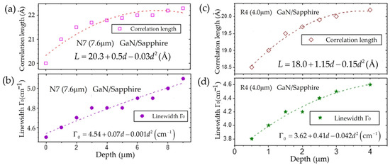
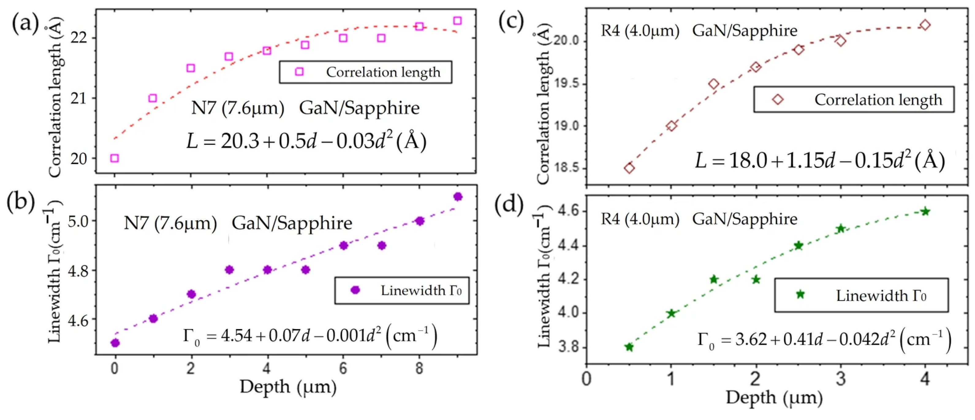
Depth d (μm) dependent spatial correlation model (SCM) fitted correlation length L (Å) and intrinsic line width Γ0 (cm−1) for GaN E2 mode of two GaN/sapphire samples of N7 (7.6 μm) at (a,b) and R4 (4.0 μm) at (c,d), respectively. All correlation length L (Å) data values are shown with open symbols and line width Γ0 (cm−1) data values are shown with solid symbols.
Table 3.
Spatial correlation model (SCM) fitted correlation length L (Å) and intrinsic line width Γ0 (cm−1) for the GaN E2 mode of the GaN/sapphire sample N7 (7.6 μm).
Table 4.
Spatial correlation model (SCM) fitted correlation length L (Å) and intrinsic line width Γ0 (cm−1) for the GaN E2 mode of the GaN/sapphire sample R4 (4.0 μm).
Raman spectral intensity I(ω) of the GaN E2(high) mode, by applying the spatial correlation model (SCM), can be described as [8,9]
where the reciprocal lattice q is in units of 2π/a, a is the lattice constant, and Γ0 is the natural or intrinsic linewidth. In the SCM, L represents an effective phonon correlation length associated with the spatial coherence of Raman-active phonons under translational-symmetry breaking. It is not equivalent to the average spacing of threading dislocations. The fitted values of 18.5–22.3 Å correspond to approximately 1.85–2.23 nm. The dispersion relation for optical phonon frequency ω(q) vs. the reciprocal lattice q has the form
where A and B are adjustable parameters [8,9]. This spatial correlation model (SCM) has been used to study many semiconductors and oxides, including SiC, InGaN, InAlN, and GaN-AlN superlattices [8].
Figure 10 and Figure 11 show the SCM fitting results for ten N7 spectra and seven R4 spectra, respectively. The experimental data are shown as blue open symbols, and the SCM fitting results are shown as red lines. Figure 10 presents the N7 spectra from d = 0 to 9 μm, whereas Figure 11 presents the R4 spectra from d = 0.5 to 4.0 μm. The fitted correlation length L (Å) and intrinsic linewidth Γ0 (cm−1) are listed in Table 3 and Table 4.
According to the values listed in Table 3 and Table 4, Figure 12 plots the graphs for depth d (μm) dependent spatial correlation model (SCM) fitted correlation length L (Å) and intrinsic line width Γ0 (cm−1) for the GaN E2 mode of GaN/sapphire sample N7 (7.6 μm) at (a)–(b) and R4 (4.0 μm) at (c)–(d), respectively. Data values in each graph are fitted by polynomials up to the second order and expressed by dashed lines. The fitted polynomial expressions are given in each graph. The SCM fits yielded L values of 20.0–22.0 Å for N7 and 18.5–20.2 Å for R4, together with Γ0 values of 4.5–5.1 cm−1 and 3.8–4.6 cm−1, respectively. These ranges summarize the model-fitted values. Because repeatability and fit-parameter uncertainties are unavailable, the apparent point-to-point changes and polynomial curvature are not interpreted as quantitatively resolved depth trends.
In contrast to Ref. [12], which correlated spatially resolved Raman shifts with independently determined dislocation density, the present study has no independent defect-density measurement. Consequently, the fitted L values are reported only as effective phonon correlation lengths and are not converted into threading-dislocation spacing or density.
3.5. Cross-Sectional Raman E1(LO)-Mode LOPC Fits
Raman LO mode is affected by free carriers and doping through LO–phonon–plasma coupling (LOPC). Theoretical studies describe the Raman LOPC mode intensity as [8,9,29,36]
where
In Equation (7), the parameters n1 and n2 represent the refractive indices at incident frequency ω1 and scattered frequency ω2, respectively. Constant C is the Faust–Henry coefficient of ~0.35, E the macroscopic electric field, α the material polarizability, and nω the Bose–Einstein population factor. For Equations (8) and (9), ωp defines the plasma frequency, ωL is the longitudinal optical (LO) phonon frequency, ωT the transverse optical (TO) phonon frequency, η the phonon damping parameter, and γ the plasma oscillation damping.
Furthermore, the dielectric response ε can be expressed as
where ωp is the plasma frequency, N the free carrier concentration, m* the effective mass, e the elementary charge, and ε∞ the high-frequency dielectric constant. Equations (7)–(12) have been applied for Raman analyses of GaN films [8,9,29,36]. Based on Equation (11), the carrier concentration is given by N = ωp2 (ε∞ m*)/(4πe2), while Equation (12) provides the mobility as μ = e/(m* γ).
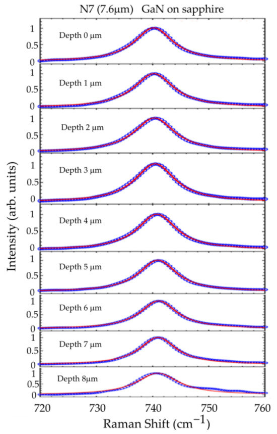
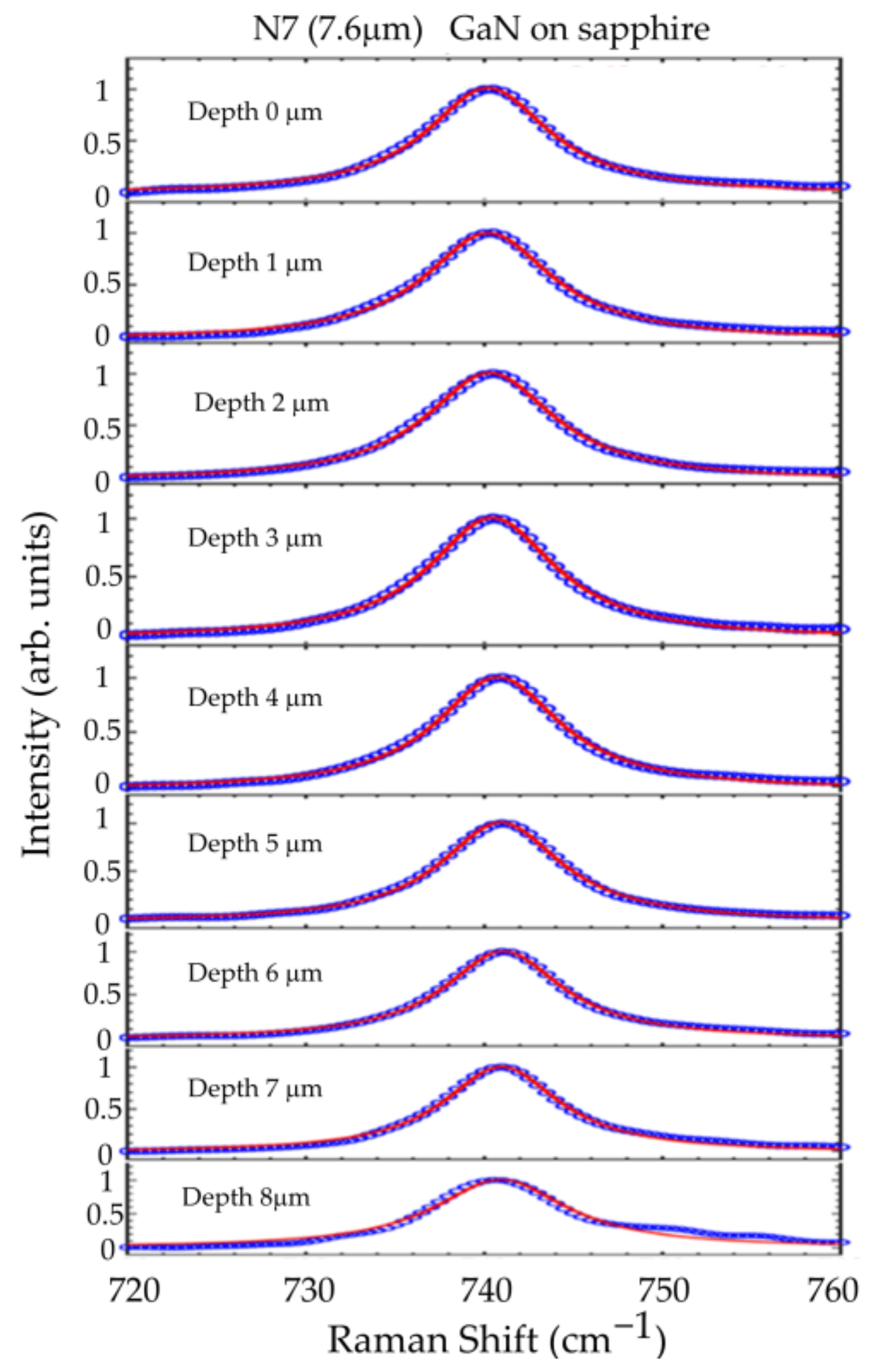
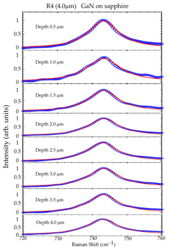
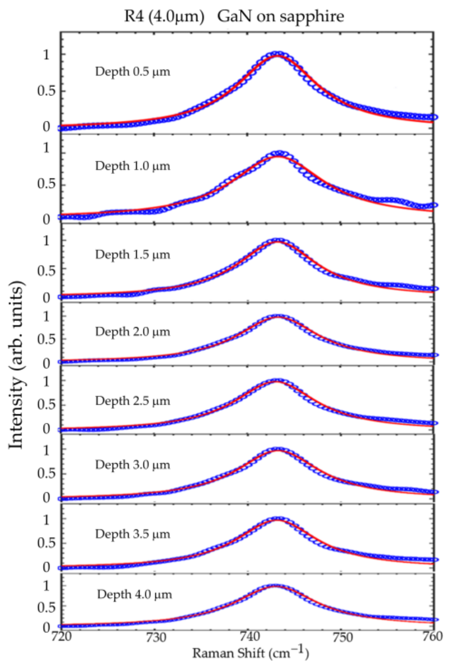
In polar semiconductors, LO phonons couple strongly to free-carrier plasmons. Using theoretical LOPC modeling, the GaN E1(LO) modes in Figure 7c and Figure 8c can be fitted [8,9,29,36] to extract carrier concentrations of GaN films on sapphire [8], Si [29] and 4H-SiC [36]. In the present work, this optical approach is employed to deduce the carrier concentration and mobility along the cross-section (growth direction) of GaN-on-sapphire films. Figure 13 and Figure 14 compare the experimental E1(LO) spectra with the LOPC-fitted curves for N7 and R4.
Figure 13.
LOPC fits for GaN/sapphire N7 (7.6 μm), with the experimental data represented by blue open symbols from Figure 7c and the fitting results indicated by red lines according to Equations (7)–(12).
Figure 14.
The LOPC fits for the GaN/sapphire sample R4 (4.0 μm), with experimental data represented by blue open symbols from Figure 8c and fitting results indicated by red lines according to Equations (7)–(12).
Table 5 and Table 6 list the LOPC fitting parameters for N7 and R4, including carrier concentration N, mobility μ, plasma frequency ωp, plasma damping rate γp, mean squared error (MSE), and root mean squared error (RMSE). MSE and RMSE characterize only the fitting residuals; they are not estimates of Raman-shift accuracy or parameter uncertainty.
Table 5.
Fitting parameters of GaN LOPC fit on RT Raman E1(LO), N7 (n7600), d = 7.6 μm.
Table 6.
Fitting parameters of GaN LOPC fit on RT Raman E1(LO), R4 (r4056), d = 4.0 μm.
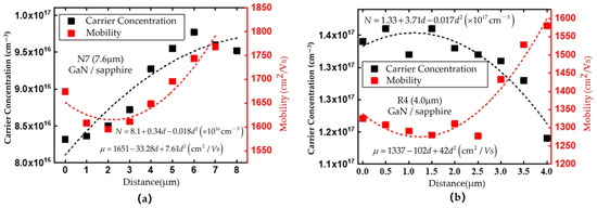
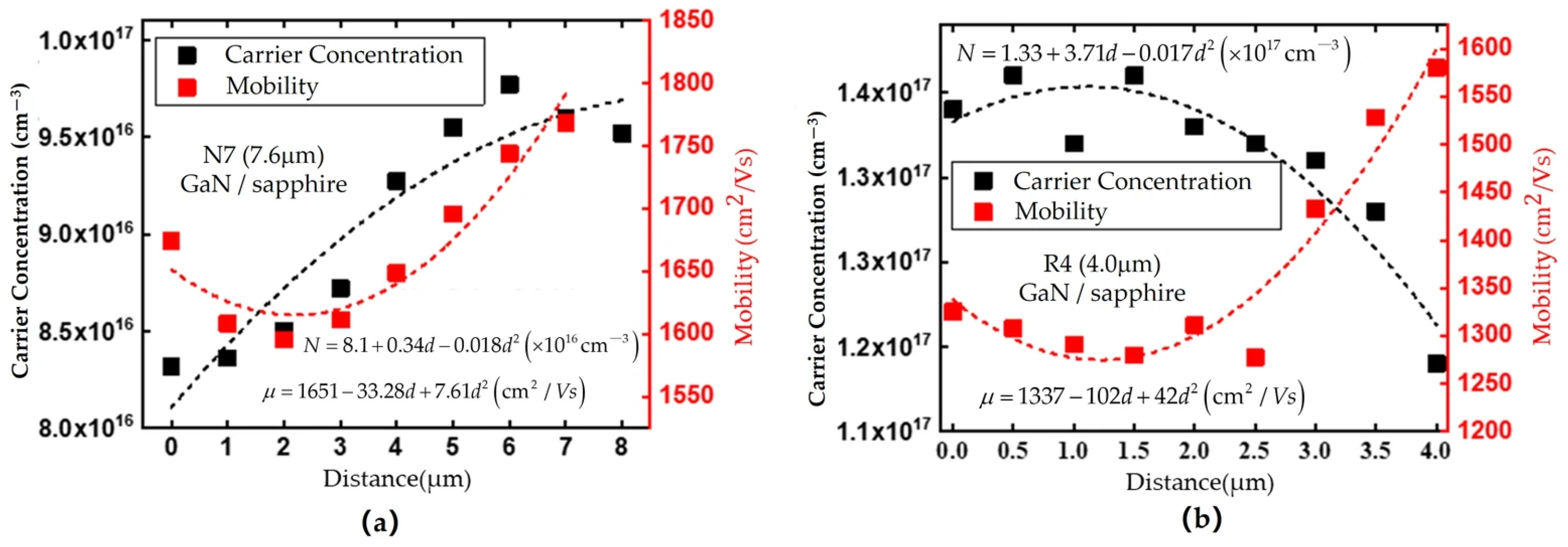
Based on the data values in Table 5 and Table 6, Figure 15 shows depth d (μm) dependent LO phonon coupling (LOPC), model-fitted carrier concentration N (cm−3) and electron mobility μ (cm2/V s) for GaN E1(LO) modes of GaN/sapphire N7 (7.6 μm) at (a) and R4 (4.0 μm) at (b), respectively. All carrier concentration N (cm−3) data values are expressed in black symbols, and mobility μ (cm2/V s) data values are in red symbols. Data values in each graph are fitted by polynomials up to the second order and expressed by dashed lines.
Figure 15.
Depth d (μm) dependent LOPC model fits carrier concentration N (cm−3) and electron mobility μ (cm2/V s) for GaN E1(LO) mode of GaN/sapphire (a) N7 (7.6 μm) and (b) R4 (4.0 μm), respectively.
Within the nominal GaN regions, the LOPC-derived carrier concentration ranges from 8.32 × 10¹⁶ to 9.77 × 1016 cm−3 for N7 and from 1.19 × 10¹⁷ to 1.36 × 1017 cm−3 for R4. The corresponding fitted mobility ranges are 1596–1769 cm2 V−1 s−1 for N7 and 1277–1580 cm2 V−1 s−1 for R4. Thus, N7 has a lower fitted carrier concentration and generally higher fitted mobility than R4.
The Raman–LOPC analysis indicates that the fitted carrier concentration and mobility do not exhibit a simple inverse relationship across the measured positions. In GaN/sapphire structures, carrier mobility may be affected not only by free-carrier concentration and plasmon damping but also by defect scattering, residual strain, dislocation-related disorder, and local crystal quality. Differences in defect distributions and unintentional impurity incorporation or compensation during epitaxial growth may contribute to the different carrier-parameter profiles of N7 and R4. However, because depth-resolved chemical-composition and independent defect-density measurements are unavailable, these mechanisms are considered possible explanations rather than direct experimental assignments. Taken together, Figure 9, Figure 12 and Figure 15 show different sample-specific fitted profiles of E2(high)-derived relative stress, SCM-derived effective phonon correlation length, and LOPC-derived carrier parameters. N7 generally exhibits lower calculated compressive stress and higher fitted mobility than R4. Ref. [15] investigated a deliberately doped GaN device using a specified confocal configuration and independently evaluated spatial resolution. In contrast, the present LOPC-derived profiles are obtained from as-grown GaN layers without independently calibrated spatial resolution or Hall validation.
4. Conclusions
This study combines cross-sectional Raman measurements with model-based analyses of carrier concentration, electron mobility, stress, and crystalline properties in two MOCVD-grown GaN/sapphire samples. Two GaN-on-sapphire samples were characterized using cross-sectional scanning electron microscopy (SEM), optical transmission (OT), and spectroscopic ellipsometry (SE), providing complementary structural and optical information. The SE-derived apparent Urbach energies were 5.79 meV for N7 and 5.91 meV for R4. Because these values are model-dependent, they are used only for comparison between the two samples and are not interpreted as direct measures of absolute defect density.
Raman spectra were acquired from the GaN surface toward the sapphire at nominal intervals of 1.0 μm for N7 and 0.5 μm for R4. The SENTERRA system calibrated each spectrum automatically and has a specified wavenumber-axis accuracy and precision better than 0.1 cm−1. Within the nominal GaN regions, the fitted E2(high) position changed by approximately +0.90 cm−1 for N7 and −0.90 cm−1 for R4. These signs are retained relative to the instrument specification, but smaller point-to-point shifts are not considered resolved because peak-fitting, focusing, spatial-averaging, and repeatability contributions are unavailable. SCM fits gave effective phonon correlation lengths of 20.0–22.3 Å for N7 and 18.5–20.2 Å for R4. LOPC fits gave carrier concentrations of 8.32 × 10¹⁶–9.77 × 1016 cm−3 for N7 and 1.19 × 10¹⁷–1.36 × 1017 cm−3 for R4, with mobility ranges of 1596–1769 and 1277–1580 cm2 V−1 s−1, respectively. The SCM and LOPC quantities are model-dependent estimates rather than independently validated measurements.
Research and Development (R&D) on GaN-on-sapphire devices remains a priority for researchers. Key characteristics of GaN films, such as carrier concentration, electron mobility, layer stress and crystalline properties, along with their variations during film growth, are critical for advanced device fabrication. These results provide a sample-specific comparison of the depth-dependent Raman-derived properties of the two GaN/sapphire structures.
Author Contributions
Conceptualization, Z.C.F. and H.-L.L.; methodology, Z.C.F. and W.L.; software, K.Y. and J.Y.; validation, G.X., I.F. and C.C.; formal analysis, M.T.N., Y.-C.C. and K.Y.; investigation, S.B., M.T.N., Y.-C.C., Z.C.F., H.-L.L. and K.Y.; resources, H.-L.L., J.L., G.X., B.K. and I.F.; data curation, Y.-C.C.; writing—original draft preparation, G.C. and Z.C.F.; writing—review and editing, M.T.N., Z.C.F. and I.F.; visualization, J.Y., W.L. and C.C.; supervision, B.K. and I.F.; project administration, H.-L.L. and C.C.; funding acquisition, H.-L.L., J.L. and C.C. All authors have read and agreed to the published version of the manuscript.
Funding
This research was funded by the National Natural Science Foundation of China (Grant No. 51972319, 52305577).
Institutional Review Board Statement
Not applicable.
Informed Consent Statement
Not applicable.
Data Availability Statement
The data that support the findings of this study are available from the corresponding author, Z.C.F., upon reasonable request.
Acknowledgments
We acknowledge the help and support provided by Shiyuan Liu, Chuanwei Zhang and Lingyu Wan, in this work. H.L.L. thanks the Higher Education Sprout Project of National Taiwan Normal University. Z.C.F. acknowledges the support while working at National Taiwan University and Guangxi University.
Conflicts of Interest
The authors declare no conflicts of interest.
References
- Melton, W.A.; Pankove, J.I. GaN growth on sapphire. J. Cryst. Growth 1997, 178, 168–173. [Google Scholar] [CrossRef] [Scilit]
- Nakamura, S.; Pearton, S.; Fasol, G. The Blue Laser Diode—The Complete Story; Springer: Berlin, Germany, 2000; Available online: https://link.springer.com/book/10.1007/978-3-662-04156-7 (accessed on 2 May 2026).
- Amano, H. Growth of GaN on sapphire via low-temperature deposited buffer layer and realization of p-type GaN by Mg doping followed by low-energy electron beam irradiation. Rev. Mod. Phys. 2015, 87, 1133–1138. (accessed on 3 May 2026). [Google Scholar] [CrossRef] [Scilit]
- Gao, X.; Huang, Y.; Wang, R.; Sun, Y.; Wang, L. Advancing flexible optoelectronics with III-nitride semiconductors: From materials to applications. Light Sci. Appl. 2026, 15, 141. [Google Scholar] [CrossRef] [Scilit] [PubMed]
- Di Paolo Emilio, M. (Ed.) GaN Technology: Materials, Manufacturing, Devices and Design for Power Conversion; Springer: Cham, Switzerland, 2024. [Google Scholar] [CrossRef] [Scilit]
- Zhou, S.; Wan, Z.; Lei, Y.; Tang, B.; Tao, G.; Du, P.; Zhao, X. InGaN quantum well with gradually varying indium content for high-efficiency GaN-based green light-emitting diodes. Opt. Lett. 2022, 47, 1291–1294. [Google Scholar] [CrossRef] [Scilit] [PubMed]
- Zhou, S.; Liao, Z.; Sun, K.; Zhang, Z.; Qian, Y.; Liu, P.; Du, P.; Jiang, J.; Lv, Z.; Qi, S. High-Power AlGaN-Based Ultrathin Tunneling Junction Deep Ultraviolet Light-Emitting Diodes. Laser Photonics Rev. 2024, 18, 2300464. [Google Scholar] [CrossRef] [Scilit]
- Feng, Z.C. Raman Scattering on Emerging Semiconductors and Oxides; CRC Press: Boca Raton, FL, USA, 2024; ISBN 9781032638874. Available online: https://www.routledge.com/9781032638874 (accessed on 16 September 2026).
- Feng, Z.C.; Wang, W.; Chua, S.J.; Zhang, P.; Williams, K.P.J.; Pitt, G.D. Raman scattering properties of GaN materials and structures under visible and ultraviolet excitations. J. Raman Spectrosc. 2001, 32, 840–846. [Google Scholar] [CrossRef] [Scilit]
- Feng, Z.C.; Li, K.; Hou, Y.T.; Zhao, J.; Lu, W.; Collins, W.E. A comparative study of high-resolution transmission electron microscopy, atomic force microscopy and infrared spectroscopy for GaN thin films grown on sapphire by metalorganic chemical vapor deposition. Surf. Coat. Technol. 2006, 200, 3224–3229. [Google Scholar] [CrossRef] [Scilit]
- Takeuchi, K.; Ogura, H.; Hasuike, N.; Kamikawa, T. Decomposition of the anisotropic strain in 3D-structure GaN layers using Raman spectroscopy. Sci. Rep. 2024, 14, 3330. [Google Scholar] [CrossRef] [Scilit] [PubMed]
- Nootz, G.; Schulte, A.; Chernyak, L.; Osinsky, A.; Jasinski, J.; Benamara, M.; Liliental-Weber, Z. Correlations between spatially resolved Raman shifts and dislocation density in GaN films. Appl. Phys. Lett. 2002, 80, 1355–1357. [Google Scholar] [CrossRef] [Scilit]
- Chaldyshev, V.V.; Pollak, F.H.; Pophristic, M.; Guo, S.P.; Ferguson, I. Micro-Raman investigation of thin lateral epitaxial overgrown GaN/sapphire(0001) films. J. Appl. Phys. 2002, 92, 6601–6606. [Google Scholar] [CrossRef] [Scilit]
- Duan, H.; Gu, W.; Zhang, J.; Hao, Y.; Chen, C.; Ni, J.; Xu, S. Characterization of GaN grown on 4H-SiC and sapphire by Raman spectroscopy and high resolution XRD. J. Semicond. 2009, 30, 073001. [Google Scholar] [CrossRef] [Scilit]
- Belyaev, A.E.; Strelchuk, V.V.; Nikolenko, A.S.; Romanyuk, A.S.; Mazur, Y.I.; Ware, M.E.; DeCuir, E.A., Jr.; Salamo, G.J. Depth profiling of strain and carrier concentration by cleaved surface scanning of GaN Gunn-diode: Confocal Raman microscopy. Semicond. Sci. Technol. 2013, 28, 105011. [Google Scholar] [CrossRef] [Scilit]
- Hong, S.; Kim, S.; Kim, H.; Song, I.; Kim, J.H.; Kim, G. Optical characterization of GaN-based LED devices through spectroscopic ellipsometry. Opt. Laser Technol. 2025, 184, 112560. [Google Scholar] [CrossRef] [Scilit]
- Suraj; Rathkanthiwar, S.; Raghavan, S.; Selvaraja, S.K. Polarization-independent grating in a GaN-on-sapphire photonic integrated circuit. Opt. Express 2023, 31, 23350–23361. [Google Scholar] [CrossRef] [Scilit] [PubMed]
- Wang, J.B.; Li, X.D.; Chen, L.; Liu, T.; Han, Z.F.; You, S.H.; Wang, L.Z.; Li, Z.L.; Hao, Y.; Zhang, J.C. Report of GaN HEMTs on 8-in Sapphire. IEEE Trans. Electron Devices 2024, 71, 4429–4432. [Google Scholar] [CrossRef] [Scilit]
- Li, S.; Zhang, H.W.; Ma, Y.F.; Wang, Q.H.; Ke, W.; Xia, Y.Y.; Wu, L.K.; Li, Y.H.; Zhu, T.G.; Ye, R.; et al. Investigation on the Isolation Approaches for High-Voltage GaN-on-Sapphire Monolithic Power Integrated Circuits. Micromachines 2025, 16, 1336. [Google Scholar] [CrossRef] [Scilit] [PubMed]
- Kinstler, A.D.; Neumann, R.; Taylor, A.A.; Besendörfer, S.; Meissner, E.; Weingärtner, R.; Brunner, F.; Brusaterra, E.; Treidel, E.B.; Schulze, J. Direct investigation of localized leakage currents in GaN-on-sapphire pn-diode. Sci. Rep. 2025, 15, 39578. [Google Scholar] [CrossRef] [Scilit] [PubMed]
- Paszkiewicz, B.K.; Paszkiewicz, B.; Dziedzic, A. Acoustic Emission from GaN-on-Sapphire Structures. Electronics 2025, 14, 4146. [Google Scholar] [CrossRef] [Scilit]
- Jose, C.; Areeckal, A.S.; Francis, A.; Awadhiya, B. Graded barrier AlGaN/GaN MOS-HEMT for ultra-sensitive and label-free detection of SARS-CoV-2. Micro Nanostruct. 2026, 209, 208379. [Google Scholar] [CrossRef] [Scilit]
- Kamiyama, M.; Rathkanthiwar, S.; Quiñones, C.E.; Mita, S.; Reddy, P.; Kirste, R.; Collazo, R.; Sitar, Z. Hole transport analysis in N-polar p-GaN. J. Appl. Phys. 2026, 139, 075706. [Google Scholar] [CrossRef] [Scilit]
- Abdullah, N.H.; Abu Bakar, A.S.; Abdul Khudus, M.I.M.; Mustaffa, M.S.; Kamarundzaman, A.; Rizuan, N.; Zaidi, N.J. The trade-off between electrical performance and structural quality in silicon (n-type) and magnesium (p-type)-doped a-plane gallium nitride (GaN) on r-plane sapphire. J. Mater. Sci. Mater. Electron. 2026, 37, 989. [Google Scholar] [CrossRef] [Scilit]
- Schmidtling, T.; Pohl, U.W.; Richter, W.; Peters, S. In situ spectroscopic ellipsometry study of GaN nucleation layer growth and annealing on sapphire in metal-organic vapor-phase epitaxy. J. Appl. Phys. 2005, 98, 033522. [Google Scholar] [CrossRef] [Scilit]
- Charles, M.B.; Kappers, M.J.; Humphreys, C.J. The effect of AlGaN and SiN interlayers on GaN/Si(111). Phys. Status Solidi C 2005, 2, 956–959. [Google Scholar] [CrossRef] [Scilit]
- Muth, J.F.; Lee, J.H.; Shmagin, I.K.; Kolbas, R.M.; Casey, H.C., Jr.; Keller, B.P.; Mishra, U.K.; DenBaars, S.P. Absorption coefficient, energy gap, exciton binding energy, and recombination lifetime of GaN obtained from transmission measurements. Appl. Phys. Lett. 1997, 71, 2572–2574. [Google Scholar] [CrossRef] [Scilit]
- Liu, W.-S.; Chang, Y.-L.; Tan, C.-Y.; Tsai, C.-T.; Kuo, H.-C. Properties of N-Type GaN Thin Film with Si-Ti Codoping on a Glass Substrate. Crystals 2020, 10, 582. [Google Scholar] [CrossRef] [Scilit]
- Feng, Z.C.; Liu, J.M.; Xie, D.; Nafisa, M.T.; Zhang, C.W.; Wan, L.Y.; Jiang, B.B.; Lin, H.H.; Qiu, Z.R.; Lu, W.J.; et al. Optical, structural and synchrotron X-ray absorption studies for GaN thin films grown on Si by molecular beam epitaxy. Materials 2024, 17, 2921. [Google Scholar] [CrossRef] [Scilit] [PubMed]
- Piccardo, M.; Li, C.K.; Wu, Y.R.; Speck, J.S.; Bonef, B.; Farrell, R.M.; Filoche, M.; Martinelli, L.; Peretti, J.; Weisbuch, C. Localization landscape theory of disorder in semiconductors. II. Urbach tails of disordered quantum well layers. Phys. Rev. B 2017, 95, 144205. [Google Scholar] [CrossRef] [Scilit]
- Chichibu, S.; Mizutani, T.; Shioda, T.; Nakanishi, H.; Deguchi, T.; Azuhata, T.; Sota, T.; Nakamura, S. Urbach–Martienssen tails in a wurtzite GaN epilayer. Appl. Phys. Lett. 1997, 70, 3440–3442. [Google Scholar] [CrossRef] [Scilit]
- Finn, R.; O’Donovan, M.; Koprucki, T.; Schulz, S. Impact of carrier-density screening on Urbach-tail energies and optical polarization in (Al,Ga)N quantum well systems. Phys. Rev. Appl. 2025, 24, 044084. [Google Scholar] [CrossRef] [Scilit]
- Ugur, E.; Ledinsky, M.; Allen, T.G.; Holovsky, J.; Vlk, A.; De Wolf, S. Life on the Urbach Edge. J. Phys. Chem. Lett. 2022, 13, 7702–7711. [Google Scholar] [CrossRef] [Scilit] [PubMed]
- Ledinsky, M.; Schönfeldova, T.; Holovsky, J.; Aydin, E.; Hajkova, Z.K.; Landova, L.; Neykova, N.; Fejfar, A.; De Wolf, S. Temperature Dependence of the Urbach Energy in Lead Iodide Perovskites. J. Phys. Chem. Lett. 2019, 10, 1368–1373. [Google Scholar] [CrossRef] [Scilit] [PubMed]
- Margueron, S.H.; Bourson, P.; Gautier, S.; Soltani, A.; Troadec, D.; De Jaeger, J.-C.; Sirenko, A.A.; Ougazzaden, A. Residual stress relaxation in GaN/sapphire circular pillars measured by Raman scattering spectroscopy. J. Cryst. Growth 2008, 310, 5321–5326. [Google Scholar] [CrossRef] [Scilit]
- Cui, C.C.; Nafisa, M.T.; Feng, Z.C.; Xu, G.; Yiin, J.; Liu, Y.; Lu, W.J.; Klein, B.; Ferguson, I.T. Spectroscopic ellipsometry and correlated studies of GaN films on 4H-SiC by MOCVD. Vacuum 2025, 240, 114589. [Google Scholar] [CrossRef] [Scilit]

Disclaimer/Publisher’s Note: The statements, opinions and data contained in all publications are solely those of the individual author(s) and contributor(s) and not of MDPI and/or the editor(s). MDPI and/or the editor(s) disclaim responsibility for any injury to people or property resulting from any ideas, methods, instructions or products referred to in the content. |
© 2026 by the authors. Licensee MDPI, Basel, Switzerland. This article is an open access article distributed under the terms and conditions of the Creative Commons Attribution (CC BY) license.