Review

Microstructured Optical Sensors: Design, Fabrication, and Applications


by
Victor Argueta-Diaz
Department of Physics and Engineering, Alma College, Alma, MI 48801, USA
Photonics 2026, 13(9), 889; https://doi.org/10.3390/photonics13090889 (registering DOI)
Submission received: 16 August 2026 / Revised: 16 September 2026 / Accepted: 16 September 2026 / Published: 19 September 2026
(This article belongs to the Special Issue Microstructured Optical Sensors: Design, Fabrication and Applications)

Abstract

Microstructured optical sensors (MOS) have emerged as transformative photonic devices offering unprecedented sensitivity, miniaturization, and multiplexing capability. This review synthesizes the state of the field for specialists in photonics and optics, covering principal design architectures—photonic crystal fibers, microresonators, plasmonic nanostructures, and integrated waveguide platforms—alongside the fabrication methodologies underpinning their realization. We examine four high-impact application domains: environmental monitoring, biomedical diagnostics, structural health monitoring, and food safety. A central argument runs through the review: the dominant bottleneck constraining MOS adoption has shifted from sensitivity—where many platforms now approach the physical detection limit—to the engineering triad of packaging difficulty, calibration drift, and manufacturing reproducibility. Against this backdrop, we provide frank comparative assessments of platform readiness for each application domain, distinguishing proof-of-concept demonstrations from deployable systems. A dedicated Critical Perspective section addresses the translation of laboratory sensitivity figures to field performance, the genuine and overstated contributions of machine learning, and a commercialization-readiness assessment for principal MOS platform families.

1. Introduction

Optical sensing has been reinvented several times since the first fiber-optic gyroscope demonstrations of the 1970s. The most recent reinvention—the introduction of microstructured geometries into the sensing element itself—has extended the range of detectable quantities, reduced device footprints, and enabled massively parallel interrogation. Yet a gap has opened between what MOS platforms can do in the laboratory and what they routinely deliver in the field. This review argues that closing that gap, rather than pushing laboratory sensitivity further, is the dominant technical challenge of the current decade.
The term microstructured optical sensor (MOS) denotes devices in which the waveguiding or resonant structure is engineered at the micro- or nanoscale to tailor light–matter interaction. This distinguishes MOS from classical fiber-optic sensors, which exploit bulk properties of a step-index fiber rather than a designed microstructure. The defining characteristic is that the spatial distribution of the electromagnetic field—and hence, the sensitivity to external perturbations—is determined primarily by fabricated geometry rather than intrinsic material properties. Several conventional, non-microstructured technologies are nonetheless treated at length in this review—fiber Bragg grating (FBG) arrays, Brillouin optical time-domain analysis (BOTDA), distributed acoustic sensing (DAS), propagating surface plasmon resonance (SPR), and fiber-based optical coherence tomography (OCT). These are included not as primary subjects but as commercialization benchmarks: each represents a mature, field-proven deployment endpoint against which the engineering readiness of true microstructured platforms is measured throughout Section 4, Section 5, Section 6, Section 7 and Section 8. This comparative framework—not platform physics in isolation—is the organizing principle of the review.
This review is not the first to survey microstructured or fiber-optic sensing technology. Existing reviews provide deep, authoritative treatment of individual platform families—photonic crystal fiber sensors [1,2], structural health monitoring with optical fiber [3,4], and waveguide-based environmental sensing [5]—or of adjacent application spaces, such as the recent survey of flexible optical waveguides for health monitoring [6]. A further recent survey specifically addresses plasmonic sensors built on photonic-crystal-fiber structures for chemical sensing [7], underscoring how active this narrower sub-field remains even as the present review’s cross-platform, cross-domain framing stays distinct from it. These works are indispensable within their respective scopes, but each evaluates platform performance primarily against laboratory sensitivity or demonstrated novel functionality. What distinguishes the present review is its organizing axis: rather than surveying platforms by physical mechanism and reporting best-case sensitivity, we organize the discussion around deployment readiness, applying a shared set of criteria—fabrication complexity, thermal stability, CMOS compatibility, and commercialization maturity—consistently across four application domains and twelve platform families (Table 1). The original contribution is this cross-platform, cross-domain, deployment-focused comparative framework, together with the explicit argument, developed in Section 8, that the field’s dominant constraint has shifted from sensitivity to engineering integration.
Progress has been driven by three converging forces. First, advances in nanofabrication—electron-beam lithography, focused-ion-beam milling, two-photon polymerization, and stack-and-draw fiber drawing—have made routine the production of structures with feature sizes well below the wavelength of light. Second, computational design tools, including FDTD and FEM solvers, now accurately predict the optical response of complex three-dimensional microstructures before fabrication. Third, integrated photonics platforms—silicon-on-insulator (SOI), silicon nitride, and lithium niobate on insulator (LNOI)—provide manufacturable substrates on which MOS elements can be co-integrated with sources, detectors, and signal-processing electronics.
The breadth of application domains covered in this review—spanning environmental monitoring, biomedical diagnostics, structural health monitoring, and food safety—reflects a deliberate editorial choice. Each domain illuminates a distinct set of engineering constraints and deployment realities; together they provide the comparative framework necessary to evaluate which platform properties actually matter across use cases. The Critical Perspective of Section 8 provides the synthesizing thread connecting these application-specific observations.
Against this background, the field faces a maturation challenge. A review of commercialization timelines across MOS platform families reveals a striking asymmetry: FBG sensors [8] and surface plasmon resonance (SPR) instruments [9] have been commercially deployed for decades, while hollow-core photonic crystal fiber gas sensors, quasi-BIC metasurface biosensors, and WGM microresonator clinical platforms—despite extraordinary laboratory demonstrations—remain largely confined to specialist research groups. The reasons are instructive: not fundamental physics limitations but packaging, temperature stabilization, surface chemistry reproducibility, and interrogator cost.
The literature underlying this review was identified through targeted, non-systematic searches of Google Scholar, IEEE Xplore, and the Optica Publishing Group database, covering publications through 2026. Search terms included combinations of “microstructured optical sensor,” “photonic crystal fiber sensor,” “microresonator biosensor,” and “plasmonic/metasurface sensor,” together with platform- and application-specific variants (e.g., “whispering-gallery mode biosensor,” “structural health monitoring fiber optic,” “food safety SERS sensor”). Eligible sources were peer-reviewed journal articles, conference proceedings, and prior review articles in English addressing the design, fabrication, or field/clinical validation of the platform families and application domains summarized in Table 1. Because this is a narrative rather than systematic review, no formal PRISMA protocol, deduplication, or dual-screening procedure was applied; source selection instead prioritized breadth across platform families and recency, with priority given to demonstrations reporting quantitative sensitivity, deployment maturity, or validated field/clinical performance.
This review is organized as follows. Section 2 surveys principal design architectures with emphasis on comparative figures of merit. Section 3 examines fabrication. Section 4, Section 5, Section 6 and Section 7 address four major application domains, each concluding with a frank platform assessment. Section 8 provides a critical perspective on laboratory-to-deployment gaps, machine learning, and commercialization readiness. Section 9 draws conclusions.
Table 1. Comparative assessment of principal MOS platform families. Deployment maturity: 1 = research only; 2 = advanced prototypes; 3 = early commercial; 4 = commercial with caveats; 5 = fully commercial with field track record. Sensitivity figures are best-demonstrated laboratory values in clean matrices; field performance is typically 1–2 orders of magnitude lower. Functional/operating range is the span of the measurand over which the platform responds usefully, as distinct from resolution (see Section 2.6); where no citable literature figure exists, the physical constraint bounding the range is stated instead of an invented number. Cost/manufacturability reflects volume scalability, not unit prototype cost.
PlatformMechanismBest Lab SensitivityFunctional/Operating RangeQ/FOMFab. ComplexityCMOS Compat.Thermal StabilityMaturity (1–5)Cost/Manuf.Key Applications
Solid-core PCF [1,10]Evanescent absorp. 10 4 RIUNot routinely reported; bounded above by mode cutoffMediumNoModerate3ModerateGas, chem, Raman
HC-ARF/HC-PCF [11]Cavity absorptionSub-ppb (lab)ppb–% conc. (Beer–Lambert-limited)HighNoNeeds stabilization2HighGas spectroscopy
WGM microsphere [12]Reactive shift∼1 fg (lab)Narrow; laser mode-hop-limited Q > 10 8 Very HighNoVery sensitive to T2Very HighResearch biosensing
WGM microtoroid [13]Reactive shiftSingle mol. (lab)Narrow; laser mode-hop-limited Q > 10 7 HighPartialNeeds stabilization2HighResearch biosensing
SOI microring [14,15]Phase/evanescent 10 5 RIU∼FSR-limited ( 10 2 10 1 RIU) Q 10 4 10 5 Low–Med.YesNeeds T control3Low (foundry)Lab-on-chip, pharma
SiN MZI/microring [16]Phase/evanescent 10 6 RIU∼FSR-limited ( 10 2 10 1 RIU)Low–Med.YesGood (low d n / d T )3Low (foundry)Biosensing, spectrosc.
Prop. SPR (Biacore) [9,17]Phase/angle shift∼1 pg mm−2 K D : pM–mM (∼12 decades)FOM ∼100LowNoModerate5MediumPharma R&D, clinical
LSPR nanoparticle [18]Near-field shift∼100 nm/RIUNarrower than SPR (short decay length)FOM ∼10–40MediumPartialSensitive to T3MediumBiosensing, environ.
Quasi-BIC metasurf. [19]Resonance shift∼500 nm/RIU (sim.)Not reported (sim. only)FOM >200Very High (EBL)NoNarrow BW1Very HighResearch only
FBG array (SMF) [8]Bragg shift∼1 μ ε strain±20,000 μ ε (±2%) [20]LowNoExcellent5Very LowSHM, temp., strain
BOTDA distributed [21]Brillouin shift∼1 °C/20 μ ε (km)Tens of km interrogation rangeLowNoGood4LowSHM, pipeline, dam
DAS ( φ -OTDR) [22]Rayleigh phaseSub-mm displace.Tens of km; strain-to-failure ∼1–2%LowNoGood5LowSHM, seismic, security

2. Design Architectures

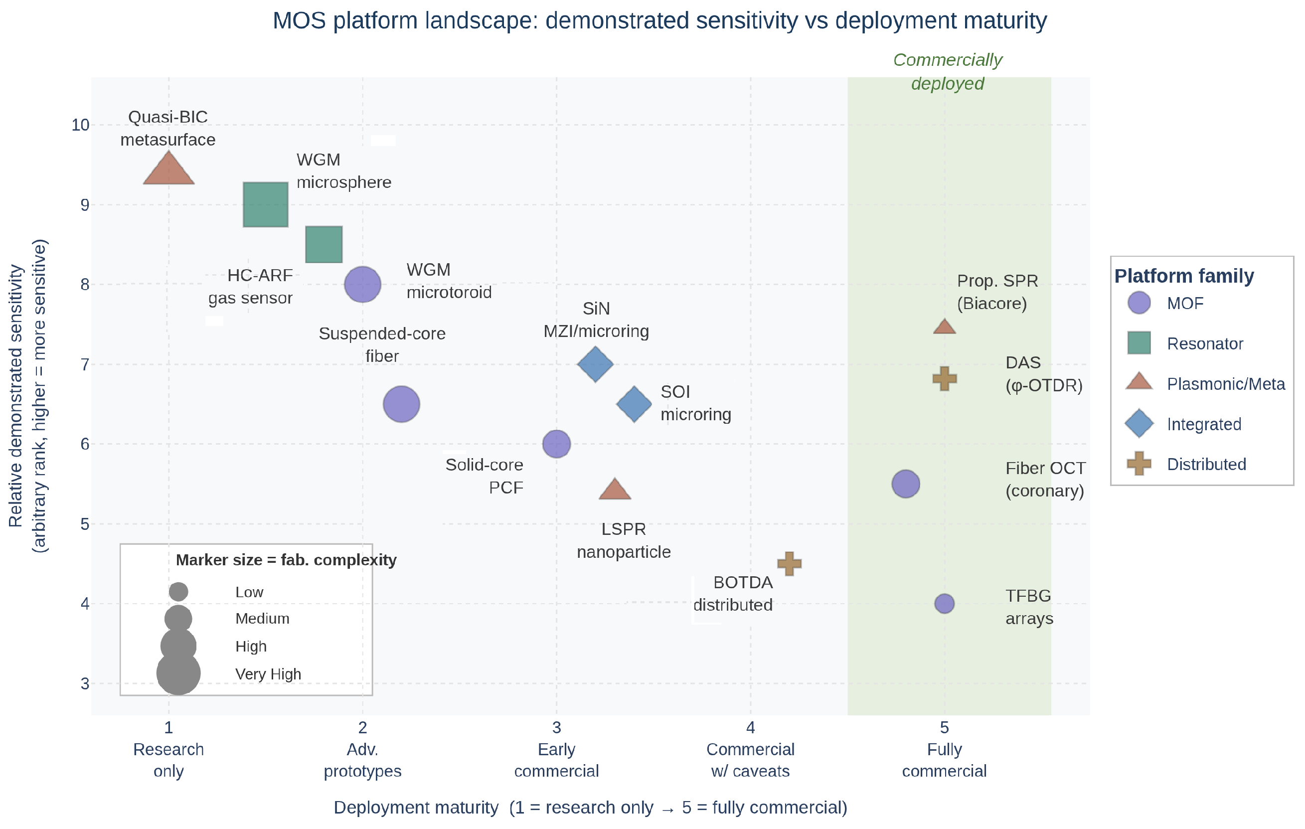
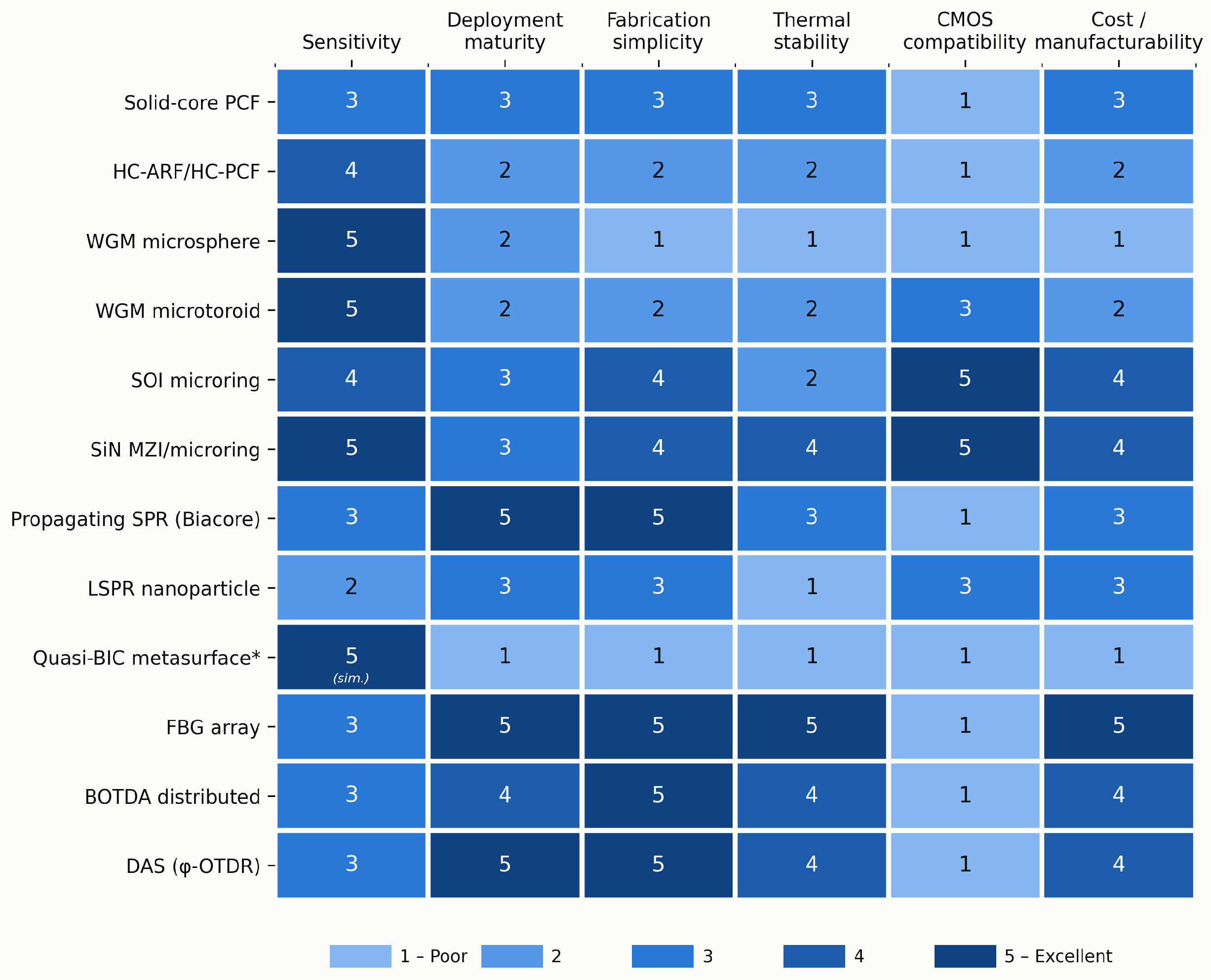
MOS platforms are not equally mature, equally manufacturable, or equally suited to each application. Understanding their comparative strengths and weaknesses—not merely their individual operating principles—is essential for platform selection. The four major architectural families are reviewed below, followed by a comparative assessment table (Table 1) and multi-criteria synthesis figures (Figure 1 and Figure 2).

2.1. Microstructured Optical Fibers

Microstructured optical fibers (MOFs), of which photonic crystal fibers (PCFs) are the canonical example [10], guide light through a periodic array of air holes running the fiber length. Two guidance mechanisms are exploited in sensing: modified total internal reflection (m-TIR) in solid-core PCFs and photonic bandgap (PBG) or inhibited-coupling guidance in hollow-core PCFs (HC-PCFs).
In solid-core PCF, the effective refractive index of the holey cladding is lower than the solid silica core, supporting m-TIR guidance. The evanescent field penetrating the air holes provides direct overlap with analyte molecules infiltrated into the cladding—sensitivities to refractive index changes of order 10 4 RIU are achievable in evanescent-absorption configurations [1]. Nonlinear optical effects, including stimulated Raman scattering [23] and supercontinuum generation, are accessible at pump powers feasible with compact laser sources.
HC-PCF confines light within a hollow core by a photonic bandgap or anti-resonant mechanism. Anti-resonant hollow-core fiber (AR-HCF) offers broader transmission windows and lower propagation loss, now around 0.11 dB/km in the near-infrared [11], making it attractive for mid-infrared absorption spectroscopy. Suspended-core fibers (SCFs) deliver strong evanescent field exposure, enabling Raman sensing in ultrasmall sample volumes. The principal limitation of MOF-based MOS is fiber-to-fiber dimensional variability affecting calibration and splice losses of 0.5–2 dB at MOF-to-SMF interfaces that are rarely accounted for in laboratory demonstrations.
The design space for periodic-microstructure sensing continues to diversify beyond the fiber geometries emphasized above. Liquid-infiltrated solid-core PCF, with a thermo-sensitive fluid replacing air in the cladding holes, has recently demonstrated highly linear temperature sensing (correlation coefficient > 0.999 across a 20–80 °C range) [24]. Two-dimensional photonic-crystal slab geometries—a related but distinct microstructure class, patterned in a planar dielectric rather than drawn into a fiber—have been proposed for simultaneous multi-analyte chemical and biological detection [25] and for dual-parameter pressure sensing in silicon and gallium arsenide [26], while one-dimensional photonic-crystal stacks have achieved sensitive trace-glycerol detection in aqueous matrices relevant to food and environmental monitoring [27]. These illustrate that the underlying design principle of this review—engineered micro/nanoscale periodicity governing sensor response—extends well beyond the specific platform families treated at length in the sections that follow.

2.2. Optical Microresonators

Optical microresonators confine light in high-Q whispering-gallery modes (WGMs) or Fabry–Pérot cavities [12]. Microsphere resonators achieve Q-factors exceeding 10 8 . Microtoroid resonators achieve comparable Q on-chip via CO2 laser reflow [13]. Microring resonators in SOI or silicon nitride have Q of 10 4 10 5 but are fully CMOS-compatible and have demonstrated on-chip single nanoparticle detection [14]. High-Q operation carries an intrinsic nonlinear penalty that headline Q-factor and sensitivity figures do not disclose. Optical absorption of the circulating intracavity power heats the resonator, and the resulting thermo-optic and thermal-expansion index shift moves the resonance itself [28]. Because the heating rate scales with the power actually coupled into the cavity—which itself depends on the pump-resonance detuning—the two effects form a positive-feedback loop: during a wavelength upscan, as the pump approaches resonance from the blue side, absorbed power rises, the resonance red-shifts to follow the pump, and coupled power rises further still. Above a threshold circulating power, this “pursuit” drags the resonance along with the scan well past where a passive (unheated) cavity would show its Lorentzian dip, producing the characteristic sawtooth-distorted lineshape and an abrupt power drop-out once heat dissipation to the environment can no longer keep pace with absorbed power—the thermal-bistability transition first characterized in silica microcavities [29]. The direct consequence for sensing is that this thermally induced, power- and scan-direction-dependent resonance shift is superimposed on the analyte-induced shift the sensor is trying to measure, and the two are not separable from a single wavelength-scan trace [28]. This is a distinct mechanism from the thermorefractive noise noted below: thermorefractive noise is a stochastic fluctuation set by ambient temperature variation and photothermal shot noise, whereas thermal bistability is a deterministic, pump-power-dependent nonlinearity intrinsic to operating any sufficiently high-Q cavity above a threshold input power. In practice, WGM biosensor demonstrations avoid this regime by operating at reduced input power, scanning slowly relative to the cavity’s thermal relaxation time, or actively locking the pump to the resonance with feedback electronics—each of which trades away signal-to-noise ratio, measurement bandwidth, or system simplicity, and none of which is typically disclosed alongside a headline Q-factor or LOD figure.
A critical qualification is warranted regarding single-molecule WGM demonstrations [1,30]. These are achieved under stringent conditions—ultraclean microfluidics, precisely controlled analyte delivery, and cryogenically stable temperature environments—incompatible with clinical or field deployment. The same resonator, functionalized with a biological recognition layer and exposed to a serum sample, loses effective Q to nonspecific binding, thermorefractive noise, and surface fouling within minutes to hours [31]. This gap between fundamental physical demonstration and practical deployable system is larger for microresonator platforms than for any other MOS family.
The fouling problem just described has a partial engineering answer, and that answer carries a quantifiable, physically distinct cost depending on which chemistry is used. Antifouling coatings resist nonspecific protein adsorption through one of two different physical mechanisms. PEG brushes work primarily through steric exclusion—an approaching protein must displace an entropically unfavorable, sterically crowded polymer layer—and require sufficient chain length and grafting density to be effective, typically yielding coating thicknesses of roughly 15–70 nm. Zwitterionic coatings (e.g., poly(carboxybetaine), poly(sulfobetaine)) instead resist fouling primarily through a tightly bound hydration shell maintained by electrostatic ion pairing between the zwitterion’s paired charges and surrounding water—an electrokinetic rather than steric mechanism—and can achieve comparable or superior fouling resistance at substantially smaller thickness: roughly 13–40 nm for carboxybetaine brushes, down to under 2 nm for the thinnest reported zwitterionic films [32].
This thickness matters directly because it competes with the evanescent field’s own decay length. For an evanescent-field sensor, the field intensity available to interact with a bound target falls off approximately as exp ( 2 z / d p ) with distance z from the surface, where d p is the field’s characteristic penetration depth—on the order of a few hundred nanometers for SPR at visible/near-infrared wavelengths [32], and of comparable order for the evanescent tails of WGM and integrated-waveguide modes. An antifouling layer of thickness t therefore imposes an approximate sensitivity penalty of exp ( 2 t / d p ) purely from displacing the binding plane outward, before any additional loss from the coating’s own optical properties: for d p 250 nm, a 40 nm carboxybetaine brush costs roughly 27% of the achievable signal and a 70 nm PEG brush roughly 43%, whereas a sub-2 nm zwitterionic film costs under 2%—broadly consistent with the 30–50% antifouling sensitivity penalty already reported for thicker coatings in Section 4.2. The practical design conclusion is that coating selection is not simply a fouling-resistance question: an ultrathin, electrokinetically stabilized zwitterionic film can outperform a thicker, sterically stabilized PEG brush on net sensitivity even where the two offer comparable fouling resistance, precisely because it sacrifices less of the evanescent field to the coating itself.

2.3. Plasmonic and Metasurface Sensors

Surface plasmon resonance (SPR) sensors couple incident photons to collective electron oscillations at a metal-dielectric interface [9]. Angular sensitivity of order 10 4  °/RIU is achievable in the Kretschmann configuration [33]. Critically, propagating SPR is the most commercially mature MOS biosensing platform: instruments from Cytiva (Biacore), Reichert, and BioNavis are deployed in pharmaceutical research worldwide and have received regulatory acceptance in drug development workflows.
Localized surface plasmon resonance (LSPR) sensors based on metallic nanoparticles exploit confined plasmon oscillations of sub-wavelength metallic inclusions. Nanohole arrays in thin metal films provide extraordinary optical transmission (EOT) [18] modulated by analyte binding. Metasurfaces supporting quasi-bound states in the continuum (quasi-BICs) achieve resonance Q-factors of 10 3 10 4 with figures of merit exceeding 200 [19,34]; however, they are not yet commercially available and require electron-beam lithography for fabrication.
A related recent design hybridizes the two mechanisms discussed above directly: a graphene metasurface combined with photonic-crystal layers has been proposed for mid-infrared refractive-index sensing [35], illustrating the continued convergence of plasmonic and photonic-crystal design principles rather than their treatment as separate platform families.
These figures conflate two physically distinct BIC mechanisms that should be distinguished explicitly. A symmetry-protected BIC exists only exactly at normal incidence, where a resonant mode’s field symmetry is incompatible with any accessible free-space radiation channel, giving—in the ideal, lossless limit—perfectly zero radiative leakage regardless of any tuning parameter. Breaking the unit cell’s in-plane mirror symmetry by a geometric asymmetry parameter α converts this ideal BIC into a quasi-BIC with finite, continuously tunable radiative quality factor obeying Q rad α 2 for small α [36]—the mechanism responsible for the Q-factors of 10 3 10 4 typical of reported dielectric-metasurface quasi-BIC sensors. An accidental (parameter-tuned) BIC, by contrast, occurs away from normal incidence, at isolated points in angle-frequency space where two or more resonances interfere destructively in the far field without requiring any special symmetry; its existence and Q-factor depend sensitively on the precise illumination angle rather than on a fixed, fabricated geometric parameter [37]. The distinction matters operationally, not just terminologically: a symmetry-protected design’s Q is set once at fabrication (via α ) and is comparatively robust to small angular misalignment near normal incidence, whereas an accidental-BIC design’s Q collapses if the illumination angle drifts from its design point—a far less forgiving requirement for a field-deployable sensor illuminated by a real, imperfectly collimated source rather than a well-aligned laboratory beam.
Of the two works cited above, ref. [19] is confirmed symmetry-protected: that design breaks symmetry via an in-plane offset Δ between a square nanohole and its enclosing silicon plate, under normal-incidence, x-polarized plane-wave illumination, exciting both a symmetry-protected BIC and a Friedrich–Wintgen BIC as Δ is tuned away from zero. It is unclear from [34]’s published abstract alone whether this design is symmetry-protected or accidental/angle-tuned—the two carry materially different robustness implications for the field-deployment discussion in Section 8.

2.4. Integrated Waveguide Platforms

Silicon-on-insulator waveguides [15] concentrate evanescent fields at the waveguide surface for bulk and surface-adsorbed analyte detection. Silicon nitride platforms offer broader transparency windows and lower propagation loss than SOI [16]. LNOI provides strong electro-optic and nonlinear-optical coefficients. The key advantage of integrated platforms is CMOS-compatible batch fabrication at wafer scale, enabling cost structures unachievable in fiber or bulk-optical formats [38,39].
The coupling interface between chip and fiber remains the principal performance bottleneck. Fiber-to-chip coupling losses of 1–3 dB per facet with a spot-size converter (e.g., an inverse taper) are both large and temperature-dependent, introducing parasitic signals indistinguishable from genuine analyte response. Thermal stabilization of the chip to sub-0.01 °C is necessary for refractive index sensing at the 10 5 RIU level, because the thermo-optic coefficient of silicon shifts the resonance by approximately 80 pm/°C [15,16].
This silicon figure is not representative of the field. Table 2 compares the thermo-optic coefficient across the core and cladding materials most common in integrated MOS platforms. Silicon’s d n / d T is roughly 7.6 × larger than silicon nitride’s and more than 20 × larger than fused silica’s—the cladding material shared by both SOI and SiN devices—while congruent lithium niobate falls between silicon nitride and silicon and is markedly anisotropic: the extraordinary-index coefficient relevant to the TE-like mode typically used in z-cut LNOI devices is several times larger than the ordinary-index coefficient at the same wavelength and temperature [40]. Because a waveguide resonance’s thermal sensitivity scales with the confinement-weighted average of the core and cladding coefficients rather than the core material alone, the practical thermal-stability advantage of a lower- d n / d T platform is smaller than the bare core-material ratio suggests whenever the guided mode extends substantially into the cladding—as is typical of the weakly confined, oxide-clad geometries used in most SiN photonic circuits. This is broadly consistent with reported SiN device thermal sensitivities running several fold, rather than a full order of magnitude, below silicon’s [41]. The practical consequence for platform selection is direct: an SOI ring requiring sub-0.01 °C stabilization for 10 5 RIU-level operation could plausibly relax to a stabilization requirement several times looser on a comparable SiN platform for the same target resolution—a genuine advantage, though smaller than the raw 7.6 × core-material ratio implies, and one traded against the weaker light–matter interaction (lower index contrast, larger mode area, longer device footprint) that lower-index-contrast platforms also carry.
These coupling losses are not merely an insertion-loss bookkeeping matter—they propagate directly into the sensor’s achievable limit of detection. For a shot-noise-limited direct-detection scheme, the minimum detectable signal scales with the inverse square root of detected optical power; a single uncompensated facet loss of 3 dB (a factor-of-two power reduction) therefore degrades the achievable LOD by roughly 2 , while the round-trip loss through two such facets—a common configuration when a chip is interrogated in reflection or read out remotely through a fiber link rather than measured with the chip adjacent to the source and detector—compounds to 6 dB and a corresponding 2 × LOD penalty. In the thermal-noise-limited receivers more typical of low-cost field interrogators, the penalty is worse: LOD degrades linearly with lost power, so the same 6 dB round-trip loss directly halves the achievable sensitivity. For genuinely remote interrogation over an extended fiber link, distributed attenuation (∼0.2 dB/km at 1550 nm) and connector losses at each patch panel accumulate on top of the facet loss and can dominate the overall link budget beyond a few kilometers. Reporting a platform’s laboratory sensitivity without stating whether it was measured chip-adjacent or through a realistic interrogation link therefore obscures a link-budget-driven sensitivity penalty that can reach several dB—this qualification should accompany the headline sensitivity figure as standard practice.

2.5. Platform Comparison

Table 1 summarizes the comparative assessment of the twelve principal MOS platform families discussed above. The deployment maturity column warrants emphasis: only propagating SPR, FBG arrays, BOTDA, and DAS-based systems score 4 or 5. The remaining platforms carry maturities of 1–3 regardless of their sensitivity achievements, reflecting the dominant role of engineering rather than physics constraints in limiting adoption.
Table 1 additionally reports each platform’s functional (operating) range—the span of the measurand over which the platform responds usefully, as distinct from its resolution (the smallest detectable change, already captured in the Best lab sensitivity column). The two are frequently conflated in laboratory reports, which typically headline resolution alone; where the literature independently establishes an operating-range figure, it is given directly and cited (fiber Bragg gratings’ strain range [20]; Biacore SPR’s affinity and kinetic-rate range [17]; the distributed-sensing interrogation lengths of BOTDA and DAS [21,22]). For the resonance-based integrated and microcavity platforms (WGM, SOI/SiN microring), no such figure is routinely reported in the literature; the entry instead states the physical mechanism that necessarily bounds it—one free spectral range before fringe-order ambiguity for the microring platforms, or the interrogation laser’s mode-hop-free scan range for WGM resonators—since a numeric estimate would otherwise be fabricated rather than sourced. Quasi-BIC metasurfaces are marked “not reported,” consistent with the sensitivity column’s existing simulation-only qualifier, since no experimental operating-range data exists for this platform in the cited literature.

2.6. Scoring Methodology

The numeric scores in Figure 2 and the qualitative ratings in Table 1 are related by an explicit rubric, summarized here to make the comparative assessments in this section traceable. Deployment maturity follows the five-tier definition given in the Table 1 caption. Fabrication simplicity and cost/manufacturability are the inverse of Table 1’s complexity and cost tiers, respectively (Low complexity → simplicity score 5; Very Low cost → manufacturability score 5). CMOS compatibility uses a three-level mapping (Yes = 5, Partial = 3, No = 1). Thermal stability follows a five-band criterion ranging from “Excellent” (5: negligible drift, no active compensation required) to “Very sensitive to T/narrow bandwidth” (1: drift dominates the signal absent non-standard stabilization, worsened by narrow resonance linewidth in high-Q platforms).
Sensitivity cannot be placed on a common numeric scale by unit conversion, since Table 1 reports fundamentally different physical quantities across platforms—refractive-index units, Q-factor, adsorbed mass, strain, and displacement are not interconvertible. The sensitivity score therefore reflects each platform’s standing relative to others measuring a comparable quantity, informed by the platform assessments developed in Section 2, Section 3, Section 4, Section 5, Section 6 and Section 7: a score of 5 denotes a platform at or defining the demonstrated frontier for its modality (e.g., single-molecule detection), while a score of 3 denotes performance comparable to established, commercially validated platforms for the same measurand. This is a qualitative synthesis judgment grounded in the cited literature, not a weighted quantitative index, and is presented as such.

3. Fabrication Methodologies

The performance of a microstructured optical sensor is inextricably linked to fabrication precision and reproducibility. A platform that achieves remarkable sensitivity in a single optimized device but cannot be reliably replicated across a production batch is unsuitable for any application requiring calibration traceability or interchangeable sensors.

3.1. Fiber Drawing and Stack-And-Draw

The stack-and-draw process assembles silica capillaries and rods in a close-packed arrangement, jacketed in an outer tube and drawn at temperatures above 1900 °C to fiber dimensions [10]. Computer-controlled pressure regulation now enables fabrication of complex, asymmetric hole lattices with sub-percent dimensional tolerances. However, lot-to-lot variation in hole geometry remains a practical challenge: for biosensing applications where the evanescent overlap integral determines sensitivity, a 2% variation in hole diameter produces a measurable sensitivity shift requiring per-batch recalibration.
Polymer MOFs (PMMA or TOPAS) draw at ∼200 °C and are amenable to solvent-based functionalization, but their higher thermo-optic coefficients and moisture sensitivity complicate field deployment. Chalcogenide and fluoride glass fibers extend transmission into the mid-infrared [11] but are brittle, humidity-sensitive, and difficult to cleave and splice—adding significant system-level complexity that laboratory demonstrations typically do not address.

3.2. Femtosecond Laser Inscription

Focused femtosecond laser pulses deposit energy in a highly localized voxel, producing permanent refractive index modifications through multiphoton ionization and structural relaxation. Point-by-point FBG inscription allows arbitrary spectral profiles and single-mode gratings in MOFs where UV-based inscription is precluded by the structured cladding [45,46]. Femtosecond-inscribed gratings in pure-silica fiber survive temperatures exceeding 1000 °C and are radiation-hard, making them the platform of choice for sensing in jet engine hot sections and nuclear environments [47]. Recent work has demonstrated AI-powered femtosecond laser inscription systems using real-time neural-network-based position correction to maintain alignment within sub-micron tolerances, enabling automated batch production of FBGs with high spectral uniformity [48].

3.3. Lithographic and Nanofabrication Routes

Planar MOS platforms leverage the full semiconductor nanofabrication toolkit: electron-beam lithography (EBL) and deep-UV projection lithography for pattern definition; reactive ion etching (RIE) and ICP-RIE for anisotropic pattern transfer; atomic layer deposition (ALD) for conformal functional layers [38]. The throughput of EBL—typically 1–10 cm2/hour at sub-100 nm resolution—is incompatible with mass production, which is why quasi-BIC metasurface sensors [19] that require EBL are unlikely to reach commercialization via this route. Nanoimprint lithography (NIL) offers a path to sub-10 nm patterning at wafer scale with throughputs compatible with volume production and deserves more attention from the MOS community.
The dimensional-tolerance treatment given above for fiber drawing (Section 3.1) and femtosecond inscription (Section 3.2) extends to the planar routes with figures that are, in relative terms, substantially tighter—though at correspondingly higher tooling cost, as quantified in Section 3.3’s throughput comparison. For 450 nm-wide silicon strip waveguides patterned by 193 nm deep-UV lithography, wafer-scale linewidth control has been demonstrated to a standard deviation of approximately 2.0 nm (0.45%) after lithography and 2.6 nm (0.56%) after pattern transfer by dry etch [49]—roughly an order of magnitude tighter in relative terms than the 2% stack-and-draw hole-diameter tolerance quoted in Section 3.1, consistent with planar lithography’s higher intrinsic dimensional precision. Atomic layer deposition extends comparable precision to layer thickness by a different mechanism: because each reaction cycle deposits a fixed, self-limiting sub-monolayer dose rather than a flux- or time-dependent film, ALD achieves reproducible sub-nanometer-per-cycle thickness control that is largely independent of the underlying topology—the property that makes it the preferred route for the conformal functional layers noted above [50].
Doping precision is the direct analog of dimensional precision for platforms requiring electronic co-integration (Section 1)—depletion-type silicon modulators and integrated photodetectors, for instance, rather than the purely passive waveguide structures discussed elsewhere in this section. For a representative depletion-mode SOI modulator, the n+/p+ implant windows must be positioned to a gap tolerance of order 40 nm to balance depletion-region overlap against series resistance, against lateral ion-straggling standard deviations of 43 nm (boron) and 36 nm (phosphorus) at typical implant energies—figures set jointly by the implanter’s dose and energy control and by the same lithographic critical-dimension tolerance quantified above, since the implant window itself is a lithographically defined feature rather than an independent process step [51]. The coupling between the two is not merely bookkeeping: in the cited optimization, correcting the implant-window design measurably improved device performance—a 4.6 dB improvement in extinction ratio and a reduction in optical loss from 3 dB to 2.5 dB for an otherwise unchanged modulator geometry. The practical implication for MOS platforms that rely on electro-optic tuning or on-chip detection is that fabrication tolerance is not a single per-platform number but a budget allocated jointly across lithographic CD control, etch fidelity, deposition thickness control, and, where applicable, implant placement—and that reporting only a headline feature-size or resolution figure, as most laboratory demonstrations do, understates the reproducibility challenge an actual foundry process must solve.
Table 3 draws the five fabrication routes discussed in this section together into a single comparison, in the same format as Table 1. No single route dominates: stack-and-draw and femtosecond inscription remain the only practical routes for in-fiber structures (MOFs, in-fiber FBGs), regardless of throughput or cost considerations, since neither EBL, DUV lithography, nor NIL can pattern a drawn fiber’s internal geometry; conversely, none of the fiber-based routes can reach the sub-100 nm, wafer-parallel patterning that planar sensing platforms—quasi-BIC metasurfaces and integrated microring/waveguide devices alike—require. Within the planar routes, the trade is explicit: EBL offers the finest, most flexible resolution but at a throughput (Section 3.3) that is fundamentally incompatible with volume production, whereas DUV projection lithography and NIL trade some resolution and flexibility for wafer-scale parallelism and correspondingly lower per-device cost. This is the same trade-off already identified for quasi-BIC metasurfaces (Section 3.3, main text) and for the deployment-maturity asymmetry running throughout this review (Section 1 and Section 8): the physics of each platform are rarely the limiting factor; the fabrication route required to realize it at volume, reproducibly, is.

3.4. Surface Functionalization

For chemical and biological sensing, the optical transducer must be coupled to a selective recognition layer. The performance of the recognition layer—not the optical transducer—frequently determines real-world sensor performance [5], particularly selectivity, fouling resistance, and long-term stability. Molecularly imprinted polymers have attracted increasing interest because they avoid the cold-chain requirements of antibody reagents and can be produced synthetically at low cost; however, their selectivity against structural analogs in complex matrices remains inferior to antibody-based recognition in most documented cases.
Two further practical distinctions deserve explicit treatment. First, binding reversibility: antibody–antigen and many aptamer–target interactions are governed by dissociation constants permitting surface regeneration—typically a brief pulse of low-pH glycine buffer or high-ionic-strength solution that disrupts non-covalent contacts without denaturing the immobilized recognition element—enabling tens to hundreds of reuse cycles before signal degradation. Covalently immobilized layers, and some high-avidity multivalent interactions, instead bind effectively irreversibly: once occupied, the site cannot be regenerated without stripping and re-functionalizing the surface, converting the device into a single-use sensor. This distinction is rarely stated explicitly in MOS papers, yet it determines whether a platform is viable for continuous or repeated-use deployment (process monitoring, wearable diagnostics) or is necessarily restricted to single-shot assays. Second, storage stability differs meaningfully between the two recognition-layer classes: antibody reagents typically require 2–8 °C storage and lose substantial binding activity within days to a few weeks at room temperature, whereas molecularly imprinted polymers (MIPs) synthesized from thermally and chemically robust polymer backbones have been shown to retain their binding capacity, with no measurable deterioration in detection limit, after at least one month of room-temperature storage with no cold-chain requirement [52]. This shelf-life advantage is a genuine, underappreciated case for MIP-based recognition in field-deployed and resource-limited settings, even though—as noted above—MIP selectivity against close structural analogs remains inferior to antibody-based recognition in most documented comparisons.

4. Environmental Monitoring

Environmental monitoring represents one of the most compelling MOS application areas, driven by regulatory demand for in situ, continuous, multi-parameter pollutant detection at trace concentrations [5].

4.1. Atmospheric Trace Gas Sensing

Mid-infrared absorption spectroscopy in HC-ARF and anti-resonant reflecting optical waveguide (ARROW) fibers have enabled detection of greenhouse gases (CO2, CH4, N2O), toxic industrial chemicals, and volatile organic compounds at sub-ppb concentrations in carefully controlled laboratory settings [53,54]. Optical frequency comb (OFC) sources permit simultaneous multi-species detection with isotopologue discrimination [55]. Cavity-enhanced absorption spectroscopy (CEAS) integrated with hollow-core fiber loops achieves effective pathlengths exceeding 1 km in a compact format. Photoacoustic spectroscopy (PAS) in microstructured fiber cavities couples optical absorption to acoustic transduction with high sensitivity at low sample volumes [56].
A qualification is essential: sub-ppb detection limits are consistently demonstrated in pure nitrogen or synthetic gas mixtures under carefully controlled pressure and temperature [53]. In realistic atmospheric monitoring, water vapor cross-sensitivity, pressure fluctuations, and aerosol interference degrade effective detection limits by one to two orders of magnitude unless compensated. The cost and power requirements of mid-IR laser sources also remain barriers to battery-operated field deployment.

4.2. Water Quality and Heavy Metal Detection

SPR sensors functionalized with ion-selective ligands have demonstrated detection limits for Pb2+, Hg2+, and As3+ ions in the sub-nanomolar range in clean buffer solutions [5,9]. Long-period gratings inscribed in PCF have been applied to monitoring oil-in-water emulsions, nitrate, and microplastic loading. In real wastewater matrices, sensor performance is substantially degraded by biological fouling within hours of immersion. Antifouling coatings partially address this but typically reduce analyte sensitivity by 30–50% in exchange for extended operational lifetime. No fiber-optic heavy metal sensor has yet demonstrated continuous unattended operation beyond 30 days in genuine wastewater—a benchmark the community should adopt as a minimum field-validation criterion.

4.3. Distributed Temperature and Strain Sensing

Brillouin optical time-domain analysis (BOTDA) and Raman OTDR in conventional and microstructured fibers have enabled distributed temperature and strain sensing over distances of tens of kilometers with meter-scale spatial resolution [21]. These systems are genuinely commercially deployed for dam monitoring, pipeline integrity assessment, and geotechnical instrumentation—making them the most operationally mature MOS technology in the environmental domain.
  • Platform Assessment. For gas sensing, HC-ARF spectroscopy [53,54] offers the best combination of sensitivity and chemical specificity in the laboratory, but field deployment is limited by mid-IR source cost, temperature stabilization requirements, and fiber fragility at connectors. For water quality, LPG-PCF sensors are promising, but surface fouling in real matrices remains the critical barrier. Distributed Brillouin/OTDR sensing in conventional SMF is by far the most field-proven option and should be the default choice unless an application specifically requires the evanescent enhancement or nonlinear-optical capabilities of MOF.

4.4. Comparison with Established Analytical Methods

It is worth situating MOS platforms against the incumbent technologies they aim to complement. For heavy-metal and ion detection, electrochemical sensors—ion-selective electrodes and anodic/cathodic stripping voltammetry—remain the field-deployment standard: inexpensive (on the order of tens to low hundreds of US dollars per sensor), requiring minimal peripheral instrumentation, and routinely achieving sub-nanomolar to nanomolar detection limits for Pb2+, Hg2+, and Cd2+ in real water matrices—performance broadly comparable to the SPR figures cited in Section 4.2 but validated over decades of field use rather than primarily in clean buffer. Their principal disadvantages are electrode fouling (a limitation they share with optical sensors), typically single-analyte-per-electrode operation that limits multiplexing relative to SPR imaging’s inherent microarray format, and periodic recalibration requirements. For gas-phase pollutants, laboratory gas chromatography–mass spectrometry (GC-MS) remains the reference method, offering superior selectivity and multi-species discrimination to any fiber-optic absorption technique but at the cost of sample collection and offline processing incompatible with continuous in situ monitoring—precisely the gap that HC-ARF and photoacoustic MOS platforms are positioned to fill, provided the water-vapor cross-sensitivity and source-cost limitations discussed in Section 4.1 are addressed. In practice, MOS platforms are unlikely to displace electrochemical or mass-spectrometric methods outright; their genuine value proposition is continuous, multiplexed, in situ monitoring at a spatial and temporal resolution that electrochemical spot-sampling and MS-based laboratory analysis cannot match, complementing rather than replacing these established methods [57,58].

5. Biomedical and Clinical Sensing

Optical biosensors offer label-free, real-time detection of biomolecular interactions with high specificity. MOS platforms have driven detection limits from nanomolar to femtomolar and below [30]—but the distance between a femtomolar detection limit in clean buffer and a validated clinical assay is the primary challenge now facing the biomedical MOS community.

5.1. Label-Free Molecular Diagnostics

SPR imaging on nanostructured gold films enables simultaneous, label-free monitoring of thousands of biomolecular binding events across a microarray, with a mass sensitivity of approximately 1 pg mm−2 in clean conditions [9]. Clinical demonstrations of SPRi-based platforms for cancer biomarkers and SARS-CoV-2 spike protein at clinically relevant concentrations have been published [59]; however, these demonstrations predominantly use spiked serum matrices rather than clinical patient samples, and few have been subjected to independent analytical validation.
WGM microresonator biosensors have achieved detection of individual proteins and single nanoparticles through the reactive sensing mechanism [14,30,60]. Silicon nitride microring arrays integrated with antibody-functionalized flow cells have been developed into multiplexed point-of-care prototypes capable of simultaneous cytokine measurement in whole blood with sub-15-min sample-to-result times [61]. The critical path to clinical translation is assay robustness: demonstrating consistent performance across recognition element lots, patient sample matrices, and instruments in different locations.

5.2. In Vivo and Implantable Sensing

Miniature PCF-based probes enable fiber-optic Raman spectroscopy of tissue at depths of several millimeters, with sufficient signal-to-noise ratio for discrimination of cancerous from healthy tissue in intraoperative settings—a capability that has seen genuine clinical translation in several academic medical centers [62]. Optical coherence tomography (OCT) probes based on GRIN-lens-terminated single-mode fiber are commercially deployed for coronary imaging [62], representing one of the genuine MOS commercial success stories in medicine. Multicore fiber shape-sensing probes for surgical robotics represent a more recent application where commercialization is under active pursuit [3].

5.3. Nucleic Acid and Single-Cell Analysis

Aptamer-functionalized resonator and SPR surfaces enable label-free nucleic acid detection through hybridization, with limits of detection in the femtomolar range in synthetic oligonucleotide systems [61]. No fully integrated MOS clinical cartridge has yet demonstrated the analytical performance, shelf stability, and manufacturing consistency required for commercial in vitro diagnostic deployment.
  • Platform Assessment. Propagating SPR is the clear leader in commercial readiness [9]—Biacore instruments are the gold standard in biopharmaceutical characterization. Integrated photonic microring arrays (SOI and SiN) [15,16] are the most credible next-generation platform: batch manufacturable with demonstrated clinically relevant prototype performance [61]. WGM microresonator and quasi-BIC platforms achieve remarkable fundamental sensitivity [19,30], but their translation to clinical instruments is blocked by temperature sensitivity, nonspecific binding, and the absence of validated sample preparation protocols rather than any fundamental physical limitation.

6. Structural Health Monitoring

Structural health monitoring (SHM) is the most commercially mature application domain in this review [3,4]. FBG arrays are embedded in bridges, dams, tunnels, wind turbines, and aircraft components as standard practice in numerous countries, with an established ecosystem of interrogators, installation standards, and field service protocols. The research frontier has moved beyond demonstrating that fiber sensors can detect structural changes to addressing data management, cross-sensitivity, and cost-per-channel challenges that limit further deployment.

6.1. Civil Infrastructure

FBG arrays embedded in prestressed concrete bridge girders provide continuous, multiplexed strain measurements, enabling lifecycle prestress-loss evaluation and real-time detection of abnormal loading events [63]. BOTDA systems have been deployed in dam bodies to monitor volumetric deformation with millimeter-resolution displacement maps [21]. Phase-sensitive OTDR ( φ -OTDR) adds a dynamic layer, detecting crack propagation events from their acoustic emission signatures without dedicated acoustic transducer hardware [3].
The primary remaining performance challenge is cross-sensitivity: strain and temperature produce Bragg wavelength shifts of comparable magnitude (approximately 1.2 pm/μ ε and 13 pm/°C at 1550 nm), and discriminating them in field conditions requires either dual-parameter sensors, reference gratings, or Brillouin-based temperature correction. High-order FBG corrosion sensors enable detection of rebar corrosion at early stages before cracking is visible [64].
This qualitative statement admits a compact quantitative form. The fractional Bragg wavelength shift of a single grating responds linearly to strain and temperature change [8]:
Δ λ B λ B = K ε ε + K T Δ T , K ε = 1 p e , K T = α Λ + α n ,
where p e is the fiber’s effective photoelastic coefficient, α Λ its thermal-expansion coefficient, and α n its thermo-optic coefficient; the figures already given above (1.2 pm/μ ε and 13 pm/°C) are K ε and K T in these units. A single grating therefore supplies one equation in the two unknowns ε and Δ T and is fundamentally unable to discriminate between them from its own reading alone. Discrimination requires a second, independent measurement whose sensitivity ratio K ε / K T differs from the first—two gratings of different core composition, cladding diameter, or host–material coupling, for instance—so that the pair of readings
Δ λ B , 1 Δ λ B , 2 = K ε , 1 K T , 1 K ε , 2 K T , 2 ε Δ T
can be inverted for ε and Δ T simultaneously [65], provided the sensitivity matrix is well-conditioned—that is, K ε , 1 / K T , 1 K ε , 2 / K T , 2 , which fails if the “second” sensor is simply a near-identical grating experiencing a scaled copy of the same strain and temperature field. The three discrimination strategies already named above map directly onto this framework rather than standing as an unconnected list: a mechanically isolated reference grating (zero applied strain by design) is the special case K ε , 2 0 , which collapses the matrix inversion to a direct temperature subtraction; a true dual-parameter sensor pair supplies two independent, non-degenerate rows of the matrix above; and Brillouin-based correction substitutes an independent, non-FBG temperature channel—the Brillouin frequency shift, whose temperature response dominates its much weaker strain response—for the second row in place of a second grating. Casting the problem this way also makes a practical failure mode explicit: the strain accuracy recovered after discrimination is not simply set by each sensor’s raw K ε resolution but is degraded by the sensitivity matrix’s condition number, so a sensor pair with similar K ε / K T ratios will amplify wavelength-measurement noise substantially in the recovered strain even when each sensor’s individual resolution looks adequate in isolation—a consideration that matters when selecting or co-locating a reference grating in the field, and one the qualitative statement above does not surface.

6.2. Wind Turbines and Offshore Structures

FBG strain sensors embedded in composite blades measure torsional and flapwise bending loads at multiple span positions, enabling real-time fatigue-life consumption models [66]. Fiber-optic Fabry-Pérot vibration sensors based on microstructured fiber tips have been demonstrated for low-frequency turbine tower monitoring, detecting sub-micron displacements with passive operation and full electromagnetic immunity [67]. DAS along subsea power cables enables simultaneous structural monitoring and marine environment surveillance from a single fiber [22]. Full-scale shaking-table validation of DAS-based SHM for offshore wind turbine towers has confirmed complementary performance of OFDR and φ -OTDR co-deployed in a single sensing fiber [67].

6.3. Aerospace and Pipeline Integrity

Femtosecond-laser-inscribed FBGs in pure silica fiber survive temperatures exceeding 1000 °C and high radiation doses encountered in jet engine hot sections and nuclear environments [47,68]. Multicore fiber shape sensing enables simultaneous measurement of bend, twist, and strain in flexible aerospace structures [3]. For pipelines, DAS-based leak detection achieves sub-meter localization over tens of kilometers, with machine learning classifiers validated in live deployments—one of the few MOS/ML integration stories where real-world performance data are publicly available [4,69].
  • Platform Assessment. FBG arrays [66] and BOTDA distributed sensing [21] are fully commercial with proven long-term deployment records. DAS [22] is in rapid commercial expansion. The dominant remaining challenge is data management: a single DAS channel generates gigabytes per hour, and real-time processing infrastructure is often the dominant project cost driver. Integration of MOS data streams with digital twin structural models [4]—rather than alarm-threshold monitoring alone—is the development that would most significantly extend the utility of these systems.

7. Food Safety and Agricultural Sensing

This is the most research-dominated application domain in this review. MOS platforms offer intrinsic advantages—label-free operation, small sample volumes, multiplexing, and portability [70]—that align well with food safety needs. However, the distance between published laboratory demonstrations and validated, regulatory compliant instruments is considerable and systematically underrepresented in the literature.

7.1. Pesticide Residue and Mycotoxin Detection

Surface-enhanced Raman scattering (SERS) sensors based on fiber-optic evanescent-wave excitation achieve sub-nanomolar detection limits for pesticide thiram in clean aqueous matrices [71]. In situ fiber SERS probes for brewed tea samples have been demonstrated with results in under five minutes without sample preparation [72]. Mycotoxin SPR biosensors with aptamer or MIP recognition layers have achieved detection limits approaching regulatory thresholds in cereals [73]. Critically, published detection limits are almost exclusively obtained in spiked clean extract matrices; independent comparisons against reference methods (LC-MS/MS) in genuine commodity matrices consistently show 3–10-fold degradation in effective sensitivity and specificity [74].

7.2. Food Adulteration and Authentication

D-shaped and square-core PCF sensors enable identification and quantification of adulterants in oils, honey, milk, and beverages [1]. Fiber-optic refractometers with machine-learning classifiers have demonstrated detection of olive oil adulterated with seed oils at concentrations as low as 2% in laboratory tests [75]. Fiber-optic SPR biosensors have been demonstrated for formalin adulteration in seafood and Sudan dye adulterants in spices [74]. The combination of SERS and fluorescence sensing in a single PCF platform enables orthogonal dual-mode verification with reduced false-positive rates [76].

7.3. Precision Agriculture and Soil Monitoring

Fiber-optic soil moisture sensors based on D-shaped fibers coated with hygroscopic metal-oxide thin films exploit the lossy mode resonance (LMR) mechanism for sensitive, reversible measurement with sensitivities exceeding 2 nm per %RH [77]. Fiber-optic SERS platforms functionalized with pathogen-specific antibodies have demonstrated sub-colony-forming-unit detection of Salmonella and E. coli O157:H7 in poultry wash samples in under 30 min in laboratory demonstrations [78].
  • Platform Assessment. The vast majority of fiber SERS [71,72] and SPR food sensors [74] are proof-of-concept demonstrations in spiked model matrices. The most commercially advanced platforms are fiber-optic SPR instruments for mycotoxin screening in grain trading [73], where regulatory thresholds are defined and the economic case for rapid testing is clear. For pesticide residue detection, the regulatory pathway from research prototype to approved official method requires multi-laboratory validation, matrix-matched calibration, and detection capability data that essentially none of the published MOS food sensor papers provide.

8. Critical Perspective: From Laboratory to Deployment

The preceding sections document an extraordinary breadth of MOS sensing capability. They also reveal a consistent pattern: the best laboratory demonstrations in every platform category have been available for several years without producing the anticipated wave of commercial adoption. This section examines the reasons directly.

8.1. The Packaging and Calibration Bottleneck

Packaging is the dominant unacknowledged cost and performance driver in MOS deployment [38]. Fiber-to-chip coupling must maintain sub-micrometer alignment across temperature excursions from 40 to + 85 °C. Standard single-mode fiber has a mode-field diameter of ∼10 μm, while SOI waveguides are typically 450 nm wide; the coupling loss (typically 3–10 dB per facet without a mode converter) is both large and temperature-dependent, introducing a parasitic signal indistinguishable from a genuine analyte response. MOF-to-standard-SMF splicing introduces losses of 0.5–2 dB reproducible to only ∼0.2 dB between installations.
Temperature stabilization requirements are particularly acute for refractive-index-based sensors. The thermo-optic coefficient of silicon ( d n / d T 1.8 × 10 4 K−1) shifts an SOI microring resonance by approximately 80 pm/°C—comparable to or larger than the target analyte signal [15,16]. The majority of demonstrated sensitivities are measured under isothermal laboratory conditions that do not reflect real use environments. Published sensor stability figures—typically measured over hours to days in laboratory buffer—are not predictive of field performance over weeks to months [5].

8.2. When Sensitivity Metrics Mislead

The MOS literature has a pervasive analytical figure-of-merit problem. Sensitivity and limit of detection (LOD) in clean buffer or synthetic gas mixture are the dominant comparative metrics, but they are the metrics least relevant to real-world utility. The metrics that actually matter—selectivity in complex matrices, reproducibility across sensor instances, long-term stability, and time-to-result—are rarely reported with sufficient rigor [5,74].
Sub-ppb gas detection results for HC-ARF spectroscopy [53,54] are routinely obtained in dry nitrogen matrices at fixed temperature and pressure. In atmospheric air with 1–2% water vapor, H2O absorption bands overlap with target analyte absorption features, increasing the effective detection limit by one to two orders of magnitude unless water vapor correction is applied. Single-molecule WGM sensing results [30] are achieved in ultraclean microfluidic systems; in clinical serum, the target molecule is present alongside ∼1012 non-target proteins per milliliter, producing a background signal overwhelming single-molecule target signals unless extremely selective recognition layers are employed. The community would benefit from adopting the convention of reporting both “clean-matrix LOD” and “matrix-matched LOD” as separate required metrics.

8.3. Machine Learning for MOS: Genuine Advances and Real Limitations

Machine learning has made genuine, validated contributions to MOS signal processing in specific, well-defined problems. Convolutional neural networks applied to BOTDA spectra have reduced frequency-shift extraction time from minutes to milliseconds with equivalent accuracy—a practical enabling advance for real-time distributed monitoring [69]. DAS event classification using deep learning has been commercially deployed for pipeline intrusion detection and has demonstrated lower false-alarm rates than rule-based classifiers on real operational datasets [69,79]. These are credible, independently validated results.
A significant fraction of MOS/ML publications, however, involve machine learning applied to problems where its contribution is more modest and less well validated. Common methodological weaknesses include training and testing on data from a single sensor run; reporting accuracy on balanced synthetic datasets; and failing to distinguish sensor drift from genuine analyte variation in time-series experiments [80]. Domain shift—the degradation in model performance when the sensor is moved to a new location, temperature regime, or analyte matrix—is almost never systematically characterized despite being the dominant failure mode in deployed ML-enabled sensors [69,80]. For an ML-assisted MOS clinical diagnostic to receive regulatory clearance, the algorithm must be validated on prospectively collected patient samples from multiple sites and paired with an explainability approach acceptable to the regulating authority [79].
An established domain-adaptation methodology exists to address exactly this failure mode, though it remains largely unapplied within the MOS literature specifically. Drift-focused approaches such as domain-adaptation extreme learning machines—which recalibrate a classifier’s decision boundary using a small amount of labeled data from the new operating condition, rather than requiring full retraining—have demonstrated substantial accuracy recovery in electronic-nose gas sensor arrays facing the same underlying problem: a chemically sensitive array whose response drifts with time, temperature, and humidity in ways closely analogous to MOS sensor drift [81]. More general adversarial domain-adaptation architectures, which train a shared feature representation to remain simultaneously discriminative for the sensing task and statistically indistinguishable across source and target operating conditions, are a further option better suited to deep-learning-based MOS pipelines [82]. Neither approach substitutes for characterizing domain shift in the first place, but their absence from the MOS/ML literature—despite an established track record in the closely related gas-sensor-array drift-compensation literature—is itself evidence that the field has not yet engaged with domain shift as a solvable engineering problem rather than an unavoidable limitation.

8.4. Commercialization Readiness Assessment

A frank assessment of commercialization status reveals a bimodal distribution. A small number of MOS technologies are genuinely commercial with multi-decade deployment track records: propagating SPR instruments [9], FBG sensor systems [8], BOTDA distributed sensors [21], DAS ( φ -OTDR) systems [22], and fiber-optic OCT probes for coronary imaging [62]. These platforms succeeded because they addressed a clear unmet need, could be manufactured reproducibly, installed and maintained by non-specialists, and produced results that users could trust and act on.
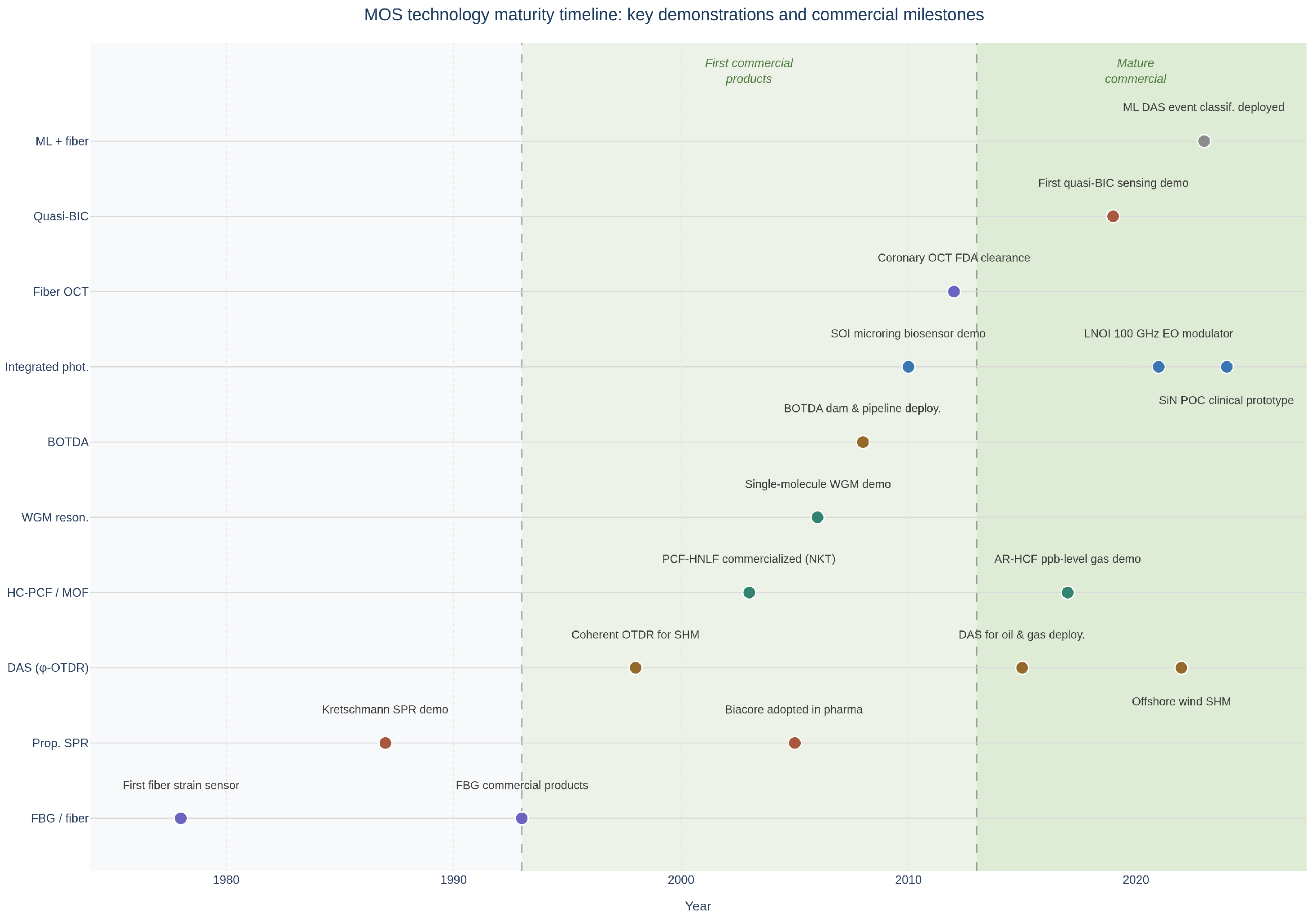
The majority of MOS platforms covered in this review—WGM microresonators [12,30], quasi-BIC metasurfaces [19], HC-PCF gas sensors [53], integrated photonic biosensor chips [15,16], fiber SERS food sensors [71,72]—are not yet commercial by this definition. The barriers are consistently at the engineering and validation level: packaging, temperature stabilization, surface chemistry reproducibility, calibration protocols, and regulatory pathways. The return on sensitivity optimization for these platforms is now marginal compared to the return on addressing the engineering bottlenecks. A more precise vocabulary would serve the field well—distinguishing between “physically demonstrated” (one group, one time), “reproduced by independent groups” (scientific validity established), “prototype system demonstrated” (engineering integration begun), and “commercially deployed” (economic and operational validity established). Figure 3 traces this commercialization trajectory across all twelve platform families, showing the pronounced gap between early laboratory demonstration and eventual commercial deployment.

9. Conclusions

Microstructured optical sensors sit at a productive inflection point: the science is mature enough to support sophisticated engineering, yet the gap between demonstrated capability and deployed performance remains wide enough to justify substantial continued investment. This review has characterized that gap honestly, using four application domains as case studies in the translation challenges faced by each major platform family.
The domains examined reveal a clear gradient of deployment maturity. Distributed sensing-based SHM [3,21,63], propagating SPR biosensing [9], and fiber OCT [62] are genuinely commercial with documented long-term operational track records. Environmental gas sensing via HC-ARF spectroscopy [53,54], integrated photonic biosensors [15,16], and food safety MOS platforms [71,72,74,75,78] are scientifically advanced but not commercially validated. WGM microresonators [12,30] and quasi-BIC metasurfaces [19] are scientifically remarkable but engineering immature, with deployment maturities of 1–2 on a five-point scale despite their sensitivity achievements.
Three conclusions are worth stating directly. First, the bottleneck has shifted: in most MOS platforms, the limiting factor for adoption is no longer sensitivity but packaging, calibration drift, and manufacturing reproducibility [5,38]. Research investment should follow this shift. Second, sensitivity metrics divorced from matrix-matched selectivity and long-term stability data are insufficient for platform comparison; the community should adopt standardized reporting requirements that include matrix-matched LOD, inter-sensor reproducibility, and minimum stability period alongside headline sensitivity figures. Third, machine learning contributes genuine, validated value in specific well-scoped problems [69,79]—BOTDA spectrum processing and DAS event classification—but is overstated in biosensing and food safety domains where domain shift [80], limited labeled datasets, and regulatory explainability requirements remain unaddressed.
The most consequential advances in the next five to ten years are likely to arise from convergence: co-integration of MOF and planar photonic elements on a single chip; coupling optical sensing with microfluidics and orthogonal transduction modalities for multiplexed multi-parameter measurements; and rigorous, independently validated machine learning applied to the large operational datasets that deployed DAS and BOTDA systems already generate. Progress on these fronts—rather than further improvements in clean-buffer detection limits—will determine whether the next wave of MOS platforms achieves the commercial traction that the current generation has not.
Translating this into a concrete forward-looking scenario, several specific milestones are plausible by 2030 if the field’s investment follows the engineering priorities identified above rather than continued sensitivity optimization. Nanoimprint lithography at wafer scale is likely to close the electron-beam-lithography throughput bottleneck identified in Section 3.3 for quasi-BIC and related metasurface sensors within this decade, enabling the first commercially credible metasurface biosensor prototypes. Co-packaged hybrid modules integrating microstructured fiber elements with planar photonic circuits—rather than the currently separate MOF and integrated photonics research tracks—are a realistic near-term convergence point, since both the fabrication tooling (Section 3.3) and the packaging challenge (Section 8.1) they must jointly solve are already well characterized. In biosensing, the critical milestone is not a further improvement in single-molecule detection limits but the first prospectively validated, multi-site clinical performance study of a WGM- or silicon-nitride-based photonic biosensor, without which regulatory translation cannot proceed regardless of further gains in laboratory sensitivity. Finally, adoption of standardized matrix-matched LOD and inter-sensor reproducibility reporting—proposed in Section 8.2—by even one major photonics or analytical chemistry journal as a submission requirement would meaningfully accelerate the field’s transition from sensitivity-competition literature to deployment-readiness literature. None of these milestones require a physics breakthrough; all are achievable engineering and methodological commitments, which is itself the central argument of this review.

Funding

This research received no external funding. The APC was funded by Alma College.

Institutional Review Board Statement

Not applicable.

Informed Consent Statement

Not applicable.

Data Availability Statement

No new data were created or analyzed in this study. Data sharing is not applicable to this article.

Acknowledgments

The authors thank the reviewers for their constructive and detailed critique, which substantially improved this manuscript.

Conflicts of Interest

The author declares no conflicts of interest.

References

  1. Chaudhary, V.S.; Kumar, D.; Pandey, B.P.; Kumar, S. Advances in photonic crystal fiber-based sensor for detection of physical and biochemical parameters—A review. IEEE Sens. J. 2023, 23, 1012–1023. [Google Scholar] [CrossRef] [Scilit]
  2. Chaudhary, V.S.; Kumar, D.; Mishra, R.; Bhardwaj, V.; Kumar, S. Photonic crystal fiber-based sensors for detection of environmental pollutants. J. Opt. 2023, 53, 1198–1221. [Google Scholar] [CrossRef] [Scilit]
  3. Bhatta, H.; Rao, Y.J.; Rao, G.S.N. Optical fiber-based SHM: Advancements, applications, and AI integration for civil infrastructure. Photonics 2025, 12, 615. [Google Scholar] [CrossRef] [Scilit]
  4. De Oliveira, R.A.; Palitó, T.; Frizera, A. Optical fiber sensors in infrastructure monitoring: A comprehensive review. Intell. Transp. Infrastruct. 2023, 2, liad018. [Google Scholar] [CrossRef] [Scilit]
  5. Butt, M.A.; Voronkov, G.S.; Grakhova, E.P.; Kutluyarov, R.V.; Kazanskiy, N.L.; Khonina, S.N. Environmental monitoring: A comprehensive review on optical waveguide and fiber-based sensors. Biosensors 2022, 12, 1023. [Google Scholar] [CrossRef] [Scilit] [PubMed]
  6. Yang, C.; Chen, S.; Zou, Y.; Ren, Y.; Wang, Z.; Xiao, K.; Leal-Junior, A.; Kumar, S.; Min, R. Flexible optical waveguides for health: A review of the current status and technological perspectives. Soft Sci. 2025, 5, 46. [Google Scholar] [CrossRef] [Scilit]
  7. Sreevani, A.; Mondal, H.; Das, N.; Soroosh, M.; Swarnakar, S. Developments in photonic crystal fiber structures-based plasmonic sensors for chemical sensing—A review. Microsyst. Technol. 2026, 32, 5. [Google Scholar] [CrossRef] [Scilit]
  8. Kersey, A.D.; Davis, M.A.; Patrick, H.J.; LeBlanc, M.; Koo, K.P.; Askins, C.G.; Putnam, M.A.; Friebele, E.J. Fiber grating sensors. J. Light. Technol. 1997, 15, 1442–1463. [Google Scholar] [CrossRef] [Scilit]
  9. Homola, J. Surface plasmon resonance sensors for detection of chemical and biological species. Chem. Rev. 2008, 108, 462–493. [Google Scholar] [CrossRef] [Scilit] [PubMed]
  10. Russell, P.S.J. Photonic crystal fibers. Science 2003, 299, 358–362. [Google Scholar] [CrossRef] [Scilit] [PubMed]
  11. Gao, S.; Wang, Y.; Ding, W.; Wang, P. Hollow-core conjoined-tube negative-curvature fibre with ultralow loss. Nat. Commun. 2018, 9, 2828. [Google Scholar] [CrossRef] [Scilit] [PubMed]
  12. Vahala, K.J. Optical microcavities. Nature 2003, 424, 839–846. [Google Scholar] [CrossRef] [Scilit] [PubMed]
  13. Halendy, M.; Ertman, S. Whispering-gallery mode micro-ring resonator integrated with a single-core fiber tip for refractive index sensing. Sensors 2023, 23, 9424. [Google Scholar] [CrossRef] [Scilit] [PubMed]
  14. Zhu, J.; Özdemir, Ş.K.; Xiao, Y.-F.; Li, L.; He, L.; Chen, D.-R.; Yang, L. On-chip single nanoparticle detection and sizing by mode splitting in an ultrahigh-Q microresonator. Nat. Photon. 2010, 4, 46–49. [Google Scholar] [CrossRef] [Scilit]
  15. Soref, R. The past, present, and future of silicon photonics. IEEE J. Sel. Top. Quantum Electron. 2006, 12, 1678–1687. [Google Scholar] [CrossRef] [Scilit]
  16. Lin, Y.; Yong, Z.; Luo, X.; Azadeh, S.S.; Mikkelsen, J.C.; Sharma, A.; Chen, H.; Mak, J.C.C.; Lo, P.G.-Q.; Sacher, W.D.; et al. Monolithically integrated, broadband, high-efficiency silicon nitride-on-silicon waveguide photodetectors. Nat. Commun. 2022, 13, 6562. [Google Scholar] [CrossRef] [Scilit] [PubMed]
  17. Cytiva Life Sciences. Kinetics and Affinity Measurements with Biacore Systems; Application Guide 29-0194-00 AE; Cytiva: Uppsala, Sweden, 2023; Available online: https://cdn.cytivalifesciences.com/api/public/content/digi-33041-pdf (accessed on 8 September 2026).
  18. Ebbesen, T.W.; Lezec, H.J.; Ghaemi, H.F.; Thio, T.; Wolff, P.A. Extraordinary optical transmission through sub-wavelength hole arrays. Nature 1998, 391, 667–669. [Google Scholar] [CrossRef] [Scilit]
  19. Jing, Z.; Wang, J.; Gao, L.; Qiu, W. High-sensitivity sensing in all-dielectric metasurface driven by quasi-bound states in the continuum. Nanomaterials 2023, 13, 505. [Google Scholar] [CrossRef] [Scilit] [PubMed]
  20. Paschotta, R. Optical Strain Sensors. In RP Photonics Encyclopedia; RP Photonics Consulting GmbH: Bad Dürrheim, Germany, 2026; Available online: https://www.rp-photonics.com/optical_strain_sensors.html (accessed on 8 September 2026).
  21. Ghazali, M.F.; Yahya, N.A.M.; Ismail, M.F.; Mahdi, M.A. State-of-the-art application and challenges of optical fibre DAS in civil engineering. Opt. Fiber Technol. 2024, 87, 103911. [Google Scholar] [CrossRef] [Scilit]
  22. Bouffaut, L.; Taweesintananon, K.; Kriesell, H.J.; Rørstadbotnen, R.A.; Potter, J.R.; Landrø, M.; Johansen, S.E.; Brenne, J.K.; Haukanes, A.; Schjelderup, O.; et al. Eavesdropping at the speed of light: Distributed acoustic sensing of baleen whales in the Arctic. Front. Mar. Sci. 2022, 9, 901348. [Google Scholar] [CrossRef] [Scilit]
  23. Benabid, F.; Knight, J.C.; Antonopoulos, G.; Russell, P.S.J. Stimulated Raman scattering in hydrogen-filled hollow-core photonic crystal fiber. Science 2002, 298, 399–402. [Google Scholar] [CrossRef] [Scilit] [PubMed]
  24. Yasini Nejad, J.; Soroosh, M.; AL-Shammri, F.K.; Alkhayer, A.G. High-sensitive and linear temperature sensor based on liquid-filled photonic crystal fiber. Opt. Quantum Electron. 2025, 57, 32. [Google Scholar] [CrossRef] [Scilit]
  25. Jesuwanth Sugesh, R.G.; Sreevani, N.R.G.; Balaji, V.R.; Soroosh, M. High-performance 2D photonic crystal sensor for simultaneous detection of chemical and biological analytes. J. Opt. 2025. [Google Scholar] [CrossRef] [Scilit]
  26. Boulesbaa, M.; Mekimah, B. A high dual-sensitivity 2D photonic crystal sensor employing Si and GaAs materials for pressure sensing. J. Mod. Opt. 2026, 73, 413–427. [Google Scholar] [CrossRef] [Scilit]
  27. Zamaninejad, F.; Tajik, F.; Ghaffari-Oskooei, S.S. High-performance 1D photonic crystal sensor for precise detection of glycerol traces in aqueous environments. Opt. Mater. 2026, 179, 118407. [Google Scholar] [CrossRef] [Scilit]
  28. Jiang, X.; Yang, L. Optothermal dynamics in whispering-gallery microresonators. Light Sci. Appl. 2020, 9, 24. [Google Scholar] [CrossRef] [Scilit] [PubMed]
  29. Carmon, T.; Yang, L.; Vahala, K.J. Dynamical thermal behavior and thermal self-stability of microcavities. Opt. Express 2004, 12, 4742–4750. [Google Scholar] [CrossRef] [Scilit] [PubMed]
  30. Vollmer, F.; Arnold, S. Whispering-gallery-mode biosensing: Label-free detection down to single molecules. Nat. Methods 2008, 5, 591–596. [Google Scholar] [CrossRef] [Scilit] [PubMed]
  31. Zossimova, E.; Jones, C.; Perera, K.M.K.; Pedireddy, S.; Walter, M.; Vollmer, F. Whispering gallery mode sensing through the lens of quantum optics, artificial intelligence, and nanoscale catalysis. Appl. Phys. Lett. 2024, 125, 030501. [Google Scholar] [CrossRef] [Scilit]
  32. D’Agata, R.; Bellassai, N.; Jungbluth, V.; Spoto, G. Recent advances in antifouling materials for surface plasmon resonance biosensing in clinical diagnostics and food safety. Polymers 2021, 13, 1929. [Google Scholar] [CrossRef] [Scilit] [PubMed]
  33. Cai, H.; Shan, S.; Wang, X. High sensitivity surface plasmon resonance sensor based on periodic multilayer thin films. Nanomaterials 2021, 11, 3399. [Google Scholar] [CrossRef] [Scilit] [PubMed]
  34. Chen, Y.; Li, Y.; Hu, Z.; Li, S.; Guo, X.; Chen, J.; Yang, H. High-performance quality factor based sensor with diagonal cylinder metasurface BIC. Photonic Sens. 2023, 13, 230232. [Google Scholar] [CrossRef] [Scilit]
  35. Maleki, M.J.; Soroosh, M.; Das, H.R.; Mondal, H.; Balaji, V.R.; Swarnakar, S. Mid-infrared graphene metasurface refractive index sensor enhanced by photonic crystal layers. Results Opt. 2026, 24, 101097. [Google Scholar] [CrossRef] [Scilit]
  36. Koshelev, K.; Lepeshov, S.; Liu, M.; Bogdanov, A.; Kivshar, Y. Asymmetric metasurfaces with high-Q resonances governed by bound states in the continuum. Phys. Rev. Lett. 2018, 121, 193903. [Google Scholar] [CrossRef] [Scilit] [PubMed]
  37. Hsu, C.W.; Zhen, B.; Stone, A.D.; Joannopoulos, J.D.; Soljačić, M. Bound states in the continuum. Nat. Rev. Mater. 2016, 1, 16048. [Google Scholar] [CrossRef] [Scilit]
  38. Shekhar, S.; Bogaerts, W.; Chrostowski, L.; Bowers, J.E.; Hochberg, M.; Soref, R.; Shastri, B.J. Roadmapping the next generation of silicon photonics. Nat. Commun. 2024, 15, 751. [Google Scholar] [CrossRef] [Scilit] [PubMed]
  39. Bogaerts, W.; Perez, D.; Capmany, J.; Miller, D.A.B.; Poon, J.; Englund, D.; Morichetti, F.; Melloni, A. Programmable photonic circuits. Nature 2020, 586, 207–216. [Google Scholar] [CrossRef] [Scilit] [PubMed]
  40. Moretti, L.; Iodice, M.; Della Corte, F.G.; Rendina, I. Temperature dependence of the thermo-optic coefficient of lithium niobate, from 300 to 515 K in the visible and infrared regions. J. Appl. Phys. 2005, 98, 036101. [Google Scholar] [CrossRef] [Scilit]
  41. Domínguez Bucio, T.; Lacava, C.; Clementi, M.; Faneca Ruedas, J.; Skandalos, I.; Galli, M.; Debnath, K.; Baldycheva, A.; Petropoulos, P.; Gardes, F. Silicon nitride photonics for the near-infrared. IEEE J. Sel. Top. Quantum Electron. 2020, 26, 1–13. [Google Scholar] [CrossRef] [Scilit]
  42. Frey, B.J.; Leviton, D.B.; Madison, T.J. Temperature-dependent refractive index of silicon and germanium. Proc. SPIE 2006, 6273, 62732J. [Google Scholar] [CrossRef] [Scilit]
  43. Arbabi, A.; Goddard, L.L. Measurements of the refractive indices and thermo-optic coefficients of Si3N4 and SiOx using microring resonances. Opt. Lett. 2013, 38, 3878–3881. [Google Scholar] [CrossRef] [Scilit] [PubMed]
  44. Rego, G. Temperature dependence of the thermo-optic coefficient of SiO2 glass. Sensors 2023, 23, 6023. [Google Scholar] [CrossRef] [Scilit] [PubMed]
  45. Chen, R.; He, J.; Xu, X.; Wu, J.; Wang, Y.; Wang, Y. High-quality fiber Bragg gratings inscribed by femtosecond laser point-by-point technology. Micromachines 2022, 13, 1808. [Google Scholar] [CrossRef] [Scilit] [PubMed]
  46. Halstuch, A.; Ishaaya, A.A. Femtosecond inscription of a fiber Bragg grating spectral array in the same spatial location. Sensors 2023, 23, 4064. [Google Scholar] [CrossRef] [Scilit] [PubMed]
  47. He, J.; Mao, Y.; Li, H. Femtosecond laser direct writing of fiber Bragg gratings for multiparameter sensing in extreme environments. APL Photon. 2023, 8, 120902. [Google Scholar]
  48. Li, H.; Yang, B.; Wang, M.; Gao, C.; Wu, B.; Zeng, L.; Xi, X.; Chen, Z.; Wang, X.; Wang, Z.; et al. Femtosecond laser fabrication of large-core fiber Bragg gratings for high-power fiber oscillators. APL Photon. 2023, 8, 046101. [Google Scholar] [CrossRef] [Scilit]
  49. Selvaraja, S.K.; Bogaerts, W.; Van Thourhout, D.; Baets, R. Fabrication of uniform photonic devices using 193 nm optical lithography in silicon-on-insulator. In Proceedings of the 20th Annual Meeting of the IEEE Lasers and Electro-Optics Society (LEOS 2007), Lake Buena Vista, FL, USA, 21–25 October 2007; pp. 48–49. [Google Scholar]
  50. George, S.M. Atomic layer deposition: An overview. Chem. Rev. 2010, 110, 111–131. [Google Scholar] [CrossRef] [Scilit] [PubMed]
  51. Yu, H.; Bogaerts, W.; De Keersgieter, A. Optimization of ion implantation condition for depletion-type silicon optical modulators. IEEE J. Quantum Electron. 2010, 46, 1763–1768. [Google Scholar] [CrossRef] [Scilit]
  52. Smolinska-Kempisty, K.; Guerreiro, A.; Canfarotta, F.; Cáceres, C.; Whitcombe, M.J.; Piletsky, S. A comparison of the performance of molecularly imprinted polymer nanoparticles for small molecule targets and antibodies in the ELISA format. Sci. Rep. 2016, 6, 37638. [Google Scholar] [CrossRef] [Scilit] [PubMed]
  53. Arman, H.; Olyaee, S.; Seifouri, M. Numerical optimization of anti-resonant hollow core fiber for high sensitivity methane detection. Sci. Rep. 2024, 14, 31534. [Google Scholar] [CrossRef] [Scilit] [PubMed]
  54. Jaworski, P.; Kozioł, K.; Krzempek, K.; Wu, D.; Yu, F.; Bojȩs, P.; Dudzik, G.; Liao, M.; Abramski, K.; Knight, J. Antiresonant hollow-core fiber-based dual gas sensor for CH4 and CO2. Sensors 2020, 20, 3813. [Google Scholar] [CrossRef] [Scilit] [PubMed]
  55. Wang, Z.; Karpf, S.; Tomizawa, K.; Becker, C.; Kordovan, A.; Schmidt, G.; Gau, M.; Kolb, C.; Huttner, W. Dual-comb spectroscopy with a single laser. Optica 2020, 7, 1536–1544. [Google Scholar]
  56. Mao, Y.; Shu, C.; Shen, T.; Wang, B.; Chen, X. Mid-infrared hollow-core fiber based flexible longitudinal photoacoustic resonator for photoacoustic spectroscopy gas sensing. Photonics 2022, 9, 895. [Google Scholar] [CrossRef] [Scilit]
  57. Zhao, G.; Tran, T.-T.; Modha, S.; Sedki, M.; Myung, N.V.; Jassby, D.; Mulchandani, A. Multiplexed anodic stripping voltammetry detection of heavy metals in water using nanocomposite-modified screen-printed electrodes integrated with a 3D-printed flow cell. Front. Chem. 2022, 10, 815805. [Google Scholar] [CrossRef] [Scilit] [PubMed]
  58. Santos, F.J.; Galceran, M.T. Modern developments in gas chromatography–mass spectrometry-based environmental analysis. J. Chromatogr. A 2003, 1000, 125–151. [Google Scholar] [CrossRef] [Scilit] [PubMed]
  59. Moznuzzaman, M.; Khan, I.; Islam, M.R. Nano-layered SPR-based biosensor for SARS-CoV-2 detection. AIP Adv. 2021, 11, 065023. [Google Scholar] [CrossRef] [Scilit] [PubMed]
  60. D’Ambrosio, D.; Avino, S.; Gagliardi, G. Direct nanoparticle sensing in liquids with free-space excited WGM microresonators. Sensors 2025, 25, 5111. [Google Scholar] [CrossRef] [Scilit] [PubMed]
  61. Toropov, N.; Cabello, G.; Serrano, M.P.; Gutha, R.R.; Rafti, M.; Vollmer, F. Review of biosensing with whispering-gallery mode lasers. Light Sci. Appl. 2021, 10, 42. [Google Scholar] [CrossRef] [Scilit] [PubMed]
  62. Bartnik, K.; Koba, M.; Śmietana, M. Advancements in optical fiber sensors for in vivo applications. Sens. Actuators B Chem. 2023, 394, 134363. [Google Scholar]
  63. Wu, R.; Biondi, A.; Cao, L.; Cui, G.; Abedin, S.; Wang, X. Composite bridge girder SHM based on distributed fiber sensing textile. Sensors 2023, 23, 4856. [Google Scholar] [CrossRef] [Scilit] [PubMed]
  64. Budinski, V.; Milivojevic, M.; Potkonjak, V.; Djordjevich, A. High-order FBG corrosion sensor based on local surface expansion detection. Struct. Control Health Monit. 2023, 2023, 9972511. [Google Scholar] [CrossRef] [Scilit]
  65. Xu, M.G.; Archambault, J.-L.; Reekie, L.; Dakin, J.P. Discrimination between strain and temperature effects using dual-wavelength fibre grating sensors. Electron. Lett. 1994, 30, 1085–1087. [Google Scholar] [CrossRef] [Scilit]
  66. Gutierrez Santiago, U.; Fernández Sisón, A.; Polinder, H.; van Wingerden, J.-W. Input torque measurements for wind turbine gearboxes using fiber-optic strain sensors. Wind Energy Sci. 2022, 7, 505–521. [Google Scholar] [CrossRef] [Scilit]
  67. Jia, Y.; Zhang, J.W.; Ye, Z.; Fu, L.; Zhang, B.; Belhora, F. Low-frequency vibration monitoring of wind turbine tower based on optical fiber sensor. Sens. Actuators A Phys. 2024, 379, 115891. [Google Scholar] [CrossRef] [Scilit]
  68. Stepanov, K.V.; Zhirnov, A.A.; Sazonkin, S.G.; Pnev, A.B.; Bobrov, A.N.; Yagodnikov, D.A. Non-invasive acoustic monitoring of gas turbine units by fiber optic sensors. Sensors 2022, 22, 2107. [Google Scholar] [CrossRef] [Scilit] [PubMed]
  69. Karapanagiotis, C.; Hicke, K.; Krebber, K. A collection of machine learning assisted distributed fiber optic sensors for infrastructure monitoring. tm-Tech. Mess. 2023, 90, 177–195. [Google Scholar] [CrossRef] [Scilit]
  70. Restuccia, A.; Leonardis, F.; Passaro, V.M.N. Innovative photonic sensors for safety and security, Part III: Environment, agriculture and soil monitoring. Sensors 2023, 23, 3225. [Google Scholar] [CrossRef] [Scilit] [PubMed]
  71. Liu, X.; Huang, L.; Ye, S.; Pan, X.; Liu, Y.; Zhao, Y. Fiber optic SERS sensor with silver nanocubes for detecting pesticide residues. ACS Appl. Mater. Interfaces 2023, 15, 24785–24794. [Google Scholar] [CrossRef] [Scilit] [PubMed]
  72. Wang, Q.; Zhang, H.; Xu, X.; Yuan, J.; Xu, Z.; Yu, X. Rapid in-situ detection of pesticide residues in tea soup with optical fiber SERS probes. Food Chem. 2024, 460, 140664. [Google Scholar]
  73. Tang, X.; Dai, Z.; Zhou, L.; Wang, Y.; Huang, X.; Zhai, X.; Zou, X.; Shi, J. Simultaneous detection of multiple mycotoxins: Recent advances in optical and electrochemical sensing. Compr. Rev. Food Sci. Food Saf. 2024, 23, e70062. [Google Scholar] [CrossRef] [Scilit] [PubMed]
  74. Osman, M.A.; Rahim, A.A.; Noor, M.I.M.; Aziz, A.A.; Akil, H.M. Recent advancement in fiber-optic-based SPR biosensor for food adulteration detection. IEEE Sens. J. 2023, 23, 15297–15309. [Google Scholar]
  75. Fernández-Fernández, E.; Pariente, J.A.; Villar-Navarro, M.; Gallegos, Á.; Ruano-López, J.M. D-shaped optical fiber refractometer for olive oil adulteration detection. Food Control 2024, 166, 110728. [Google Scholar] [CrossRef] [Scilit]
  76. Paget, B.M.; Ram, K.V.; Bhowmick, S. PCF-based fluorescence sensing for chemical and biomedical applications. Sens. Actuators B Chem. 2023, 399, 134816. [Google Scholar]
  77. Tien, C.-L.; Shih, H.-F.; Tien, J.-K.; Wang, C.-C. High-sensitivity fiber optic soil moisture sensor based on D-shaped fiber and SnO2 thin film. Sensors 2024, 24, 7474. [Google Scholar] [CrossRef] [Scilit] [PubMed]
  78. El-Khoury, M.; Sherif, S.; Liu, C.; Bhattacharya, M.; Bhattacharya, S.K.; Bhattacharya, R. Fiber optics-based SERS sensors for multiplex detection of foodborne pathogens in raw poultry. Microsyst. Nanoeng. 2024, 10, 155. [Google Scholar] [CrossRef] [Scilit] [PubMed]
  79. Pryamikov, A. Deep learning as a highly efficient tool for digital signal processing design. Light Sci. Appl. 2024, 13, 259. [Google Scholar] [CrossRef] [Scilit] [PubMed]
  80. Venketeswaran, A.; Lalam, N.; Wuenschell, J.; Ohodnicki, P.R.; Badar, M.; Chen, K.P.; Lu, P.; Duan, Y.; Chorpening, B.; Buric, M. Recent advances in machine learning for fiber optic sensor applications. Adv. Intell. Syst. 2022, 4, 2100067. [Google Scholar] [CrossRef] [Scilit]
  81. Zhang, L.; Zhang, D. Domain adaptation extreme learning machines for drift compensation in E-nose systems. IEEE Trans. Instrum. Meas. 2015, 64, 1790–1801. [Google Scholar] [CrossRef] [Scilit]
  82. Ganin, Y.; Ustinova, E.; Ajakan, H.; Germain, P.; Larochelle, H.; Laviolette, F.; Marchand, M.; Lempitsky, V. Domain-adversarial training of neural networks. J. Mach. Learn. Res. 2016, 17, 1–35. [Google Scholar]
Figure 1. MOS platform landscape: demonstrated sensitivity versus deployment maturity. Marker shape encodes platform family; marker size encodes fabrication complexity. The green-shaded zone indicates commercially deployed systems. The pronounced gap between high-sensitivity, low-maturity platforms (upper left) and deployed systems (right) illustrates the central argument of this review: engineering constraints, not physics, are the dominant barrier to MOS adoption.
Photonics 13 00889 g001
Figure 2. Multi-criteria comparison of principal MOS platform families across six dimensions: sensitivity, deployment maturity, fabrication simplicity, thermal stability, CMOS compatibility, and cost/manufacturability. Scores are 1 (poor) to 5 (excellent), assigned according to the rubric defined in Section 2.6. Platforms are shown in the same order as Table 1 rather than ranked by a composite score, since the six dimensions are not equally weighted toward any single deployment outcome. Two distinct profiles emerge rather than one dominant platform family: distributed sensing platforms (FBG, BOTDA, DAS) and propagating SPR lead on deployment maturity, fabrication simplicity, thermal stability, and cost, but none are CMOS-foundry compatible; integrated photonics platforms (SOI, SiN) instead lead on CMOS compatibility while matching them on cost and fabrication simplicity, trading lower current deployment maturity for a foundry-scalable manufacturing path. Quasi-BIC’s sensitivity score reflects a simulated, not experimentally demonstrated, figure of merit.
Photonics 13 00889 g002
Figure 3. Technology maturity timeline for principal MOS platform families: key demonstration and commercial milestones from late 1970s to early 2026. The green-shaded zones indicate the periods of first commercial products (from ∼1993) and mature commercial markets (from ∼2013). Platforms at the lower portion of the chart (FBG [8], propagating SPR [9], DAS, BOTDA) accumulated commercial milestones decades before the research-stage platforms shown above them.
Photonics 13 00889 g003
Table 2. Comparative thermo-optic coefficients of common integrated photonic waveguide materials near 1550 nm and room temperature.
Material dn / dT ( × 10 5  K−1)Reference
Silicon (Si)18.7[42]
Lithium niobate (LiNbO3, extraordinary)3.3[40]
Silicon nitride (Si3N4) 2.45 ± 0.09 [43]
Fused silica (SiO2) 0.82 0.85 [44]
Table 3. Comparison of the principal fabrication routes discussed in Section 3. Throughput and cost are qualitative tiers, following the same convention as Table 1’s Fab. complexity and Cost/manuf. columns; resolution/tolerance figures are best-demonstrated literature values.
RouteTypical Resolution/ToleranceThroughputTooling CostMaterials CompatibilityBest Suited to
Stack-and-draw [10]Sub-% dimensional control; 2% hole-diameter lot-to-lot variation typicalHigh (km of fiber per draw, once preform is made)Low–MediumSilica, soft/chalcogenide glass, polymers (PMMA, TOPAS)MOFs, in-fiber sensing elements
Femtosecond direct-write [45,46,48]Sub-μm voxel; sub-μm alignment with AI-corrected positioningLow–Medium (serial, point-by-point; improving with automation)Medium–High (ultrafast laser system)Any transparent medium (glass, polymer, crystal); works inside drawn MOFsIn-fiber FBGs, harsh-environment gratings, MOF cladding-incompatible inscription
Electron-beam lithography (EBL)Sub-100 nm, down to a few nm CD in the best demonstrationsVery Low (∼1–10 cm2/h)Very HighPlanar substrates (Si, SiN, resist-compatible dielectrics)Quasi-BIC metasurfaces, research-scale planar prototypes
DUV (193 nm) projection lithography [49]∼2 nm linewidth std. dev. (0.45%) demonstrated at wafer scaleHigh (wafer-parallel, foundry-standard)Medium (shared foundry tooling)CMOS-compatible planar substrates (SOI, SiN)Volume-manufacturable integrated waveguide/microring sensors
Nanoimprint lithography (NIL)Sub-10 nm patterning demonstrated at wafer scaleHigh (wafer-scale, volume-compatible)Low–Medium (mold reused across wafers)Polymers, sol-gel, and UV-curable resists on planar substratesVolume-scale replication of planar nanophotonic patterns once a master mold exists
Disclaimer/Publisher’s Note: The statements, opinions and data contained in all publications are solely those of the individual author(s) and contributor(s) and not of MDPI and/or the editor(s). MDPI and/or the editor(s) disclaim responsibility for any injury to people or property resulting from any ideas, methods, instructions or products referred to in the content.