


Abstract
This paper presents a waveguide energy-selective device operating in the Ku band. By utilizing the nonlinear characteristics of PIN diodes, the device can autonomously switch its operating state according to the power level of incident signals inside the waveguide, achieving an adaptive transmission response. Concurrently, through a dual-layer structural design and optimized inter-layer coupling, it enables the device to deliver broadband-protective performance within the Ku band. To validate its feasibility, the device was designed and implemented based on the waveguide WR62. The results indicate that during the transmission of a −10 dBm signal, the device exhibits insertion loss fluctuating around 1 dB within the 13–17 GHz band, whereas under 45 dBm signal incidence, the shielding effectiveness exceeds 10 dB across this frequency range. The device can be integrated into waveguides to provide adaptive high-power protection, thus demonstrating significant application potential in the field of electromagnetic protection for sensitive electronic equipment.
1. Introduction
High-power radiation from large-scale wireless stations poses a serious threat to electronic equipment. It not only interferes with the normal operation of electronic components, but can also cause irreversible damage to the equipment. This has attracted widespread attention, particularly in the research of high-power radiation shielding methods [1,2,3,4]. Conventionally, EM shielding methods mainly include limiters [5,6,7], filters [8,9], and frequency-selective surfaces (FSSs) [10,11,12,13]. However, these methods are unable to ensure the normal transmission and reception of operational signals while preventing harmful signals from damaging electronic components.
To address the requirements for nonlinear protection, Yang et al. proposed the concept of the energy-selective surface (ESS) in 2013 [14]. The operational principle of the ESS is realized through the coupling of incidental electromagnetic waves by structure, which induces voltages and currents to drive nonlinear components for adaptive impedance modulation. This enables the efficient reception of operational signals while protecting the system from high-power radiation. In recent years, researchers have expanded the functionality of ESSs by employing diverse structures and novel materials, including ultra-broadband technology [15,16,17,18], high-performance design [19,20,21,22], nonreciprocal design [23,24], implementation based on vanadium dioxide [25,26], and other innovations [27]. The ESS is typically integrated onto the radome to achieve protective functionality. However, for large-aperture antennas or their arrays, the implementation requires installing numerous nonlinear components, which may lead to increased manufacturing costs and degraded protective performance.
In comparison with space field protection, implementing high-power electromagnetic protection within a waveguide is another effective approach. Rectangular waveguides are conventionally utilized as transmission lines in the front ends of radar and other electronic systems, which eliminates the need to consider the antenna structural dimensions in the design of waveguide protective devices. In recent years, researchers have developed various waveguide protective devices, including waveguide limiters [28,29,30], ferrite limiters [31], and plasma waveguide limiters [32]. However, the aforementioned devices require permanent fixation to the waveguide, thus restricting their application scope. To address this limitation, a series of studies and designs related to waveguide energy-selective devices have been conducted by researchers [33,34,35,36,37,38]. However, existing research on waveguide energy-selective devices predominantly concentrates on the L and S bands. As the operational frequencies of modern electronic equipment continue to expand into the Ku band and higher-frequency ranges, waveguide energy-selective devices designed for lower-frequency bands are inadequate to meet the protection requirements of high-frequency application scenarios. Moreover, in the design and implementation of waveguide energy-selective devices at higher frequencies, issues such as relatively high insertion loss (IL) and narrow operating bandwidth are commonly encountered, which further limit their practical application in high-frequency, broadband electronic information systems.
In this paper, a waveguide energy-selective device operating in the Ku band is proposed. Leveraging the nonlinear characteristics of PIN diodes, the proposed structure can autonomously switch its operating state according to the incident power level within the operating band, thereby achieving adaptive high-power protection. By employing a dual-layer architecture and optimizing the inter-layer coupling effect, the device attains broadband-protective performance across the Ku band. The experimental results show that under low-power signals, the device can achieve IL fluctuating around 1 dB across the 13–17 GHz frequency band, while simultaneously providing effective shielding against high-power signals, with a shielding effectiveness (SE) exceeding 10 dB throughout this frequency range. The proposed waveguide energy-selective device exhibits a higher operating frequency band and broader protection bandwidth, thereby demonstrating significant application potential in high-frequency and broadband protection fields.
2. Design and Simulation of the Proposed Structure
2.1. Structural Design
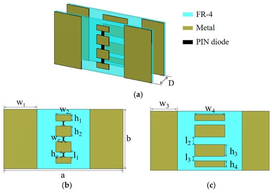
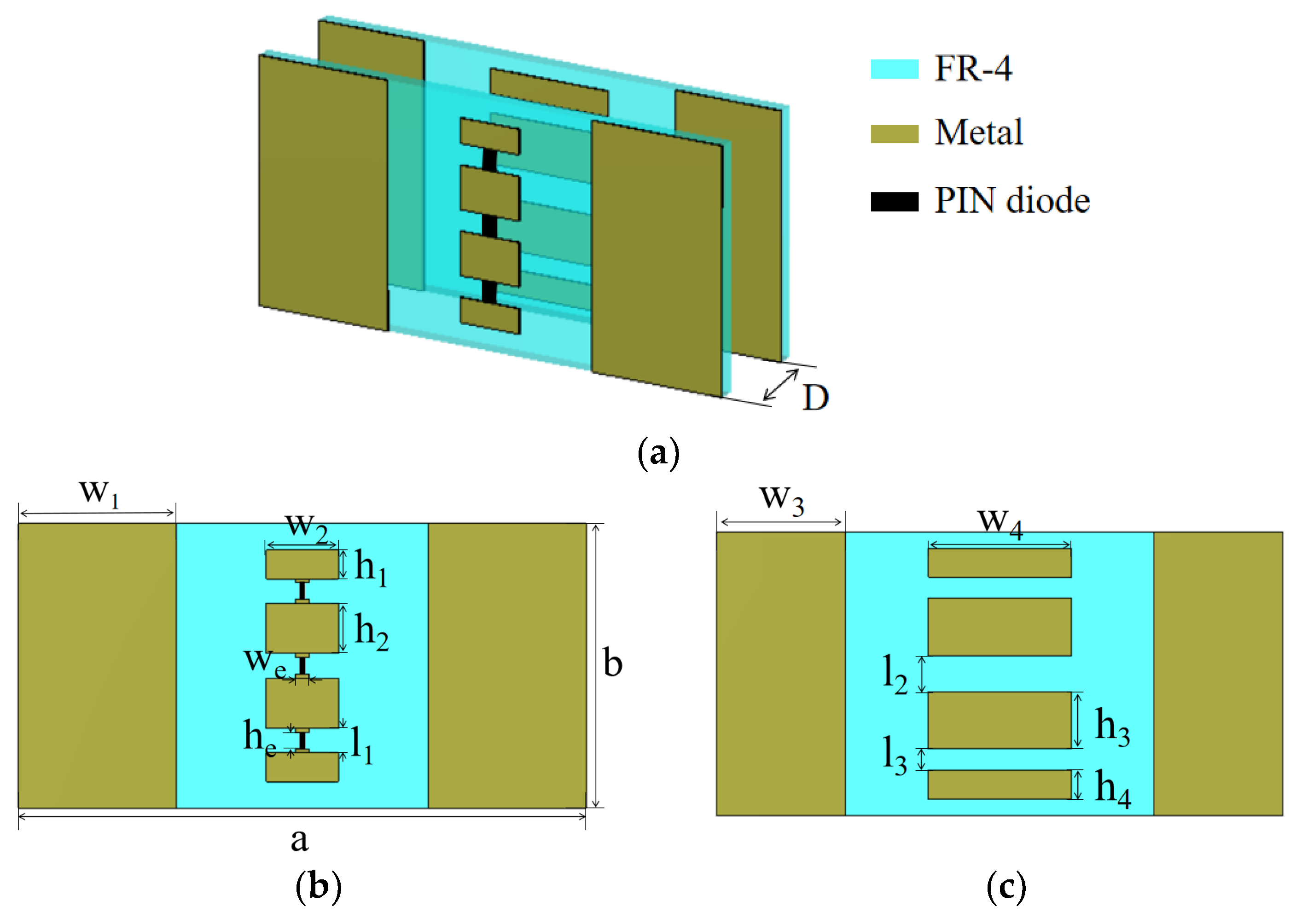
The model of the waveguide energy-selective structure presented in this paper is illustrated in Figure 1. It consists of a dual-layer structure, each with an FR-4 dielectric substrate with a relative permittivity εr = 4.3 and a thickness of h. Furthermore, two layers are separated by an air layer with a thickness of D. On the surfaces of both substrate layers, multiple centrosymmetric metal patches are printed. Subsequently, three PIN diodes are integrated into the gaps between the patches on the first layer, enabling the structure to provide a nonlinear transmission response to varying input power levels. The three integrated PIN diodes must be aligned with uniform polarity orientation. The waveguide energy-selective structure is optimized using CST, with the final dimensions summarized in Table 1.
Figure 1.
Structural model of the proposed device. (a) Three-dimensional view. (b) Front view of the first layer. (c) Front view of the second layer.
Table 1.
Structural parameters of the proposed device.
2.2. Performance Metrics
In this paper, IL and SE are adopted as the fundamental parameters for evaluating device performance. Based on the operating state of the device under different excitation conditions, these two key performance indicators are defined as follows. Under low-power signal incidence, which is insufficient to turn on the PIN diodes, the device remains in a transmission state. In this case, the IL is defined as the ratio of the incident wave to the transmitted wave, which is numerically equal to . A smaller IL value indicates lower signal transmission loss. When high-power signals are incident, the increased voltage and current induced on the metallic structures drive the PIN diodes into the ON-state, and the device correspondingly switches to a shielding state. Under this condition, the SE is defined as the ratio of the incident wave to the transmitted wave, also corresponding numerically to . A larger SE value indicates a stronger shielding capability of the device against the incident signal.
2.3. Simulation Setup
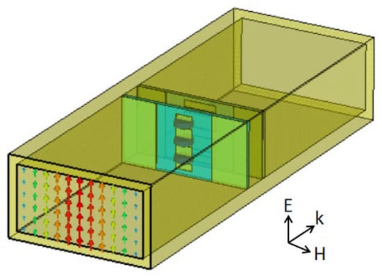
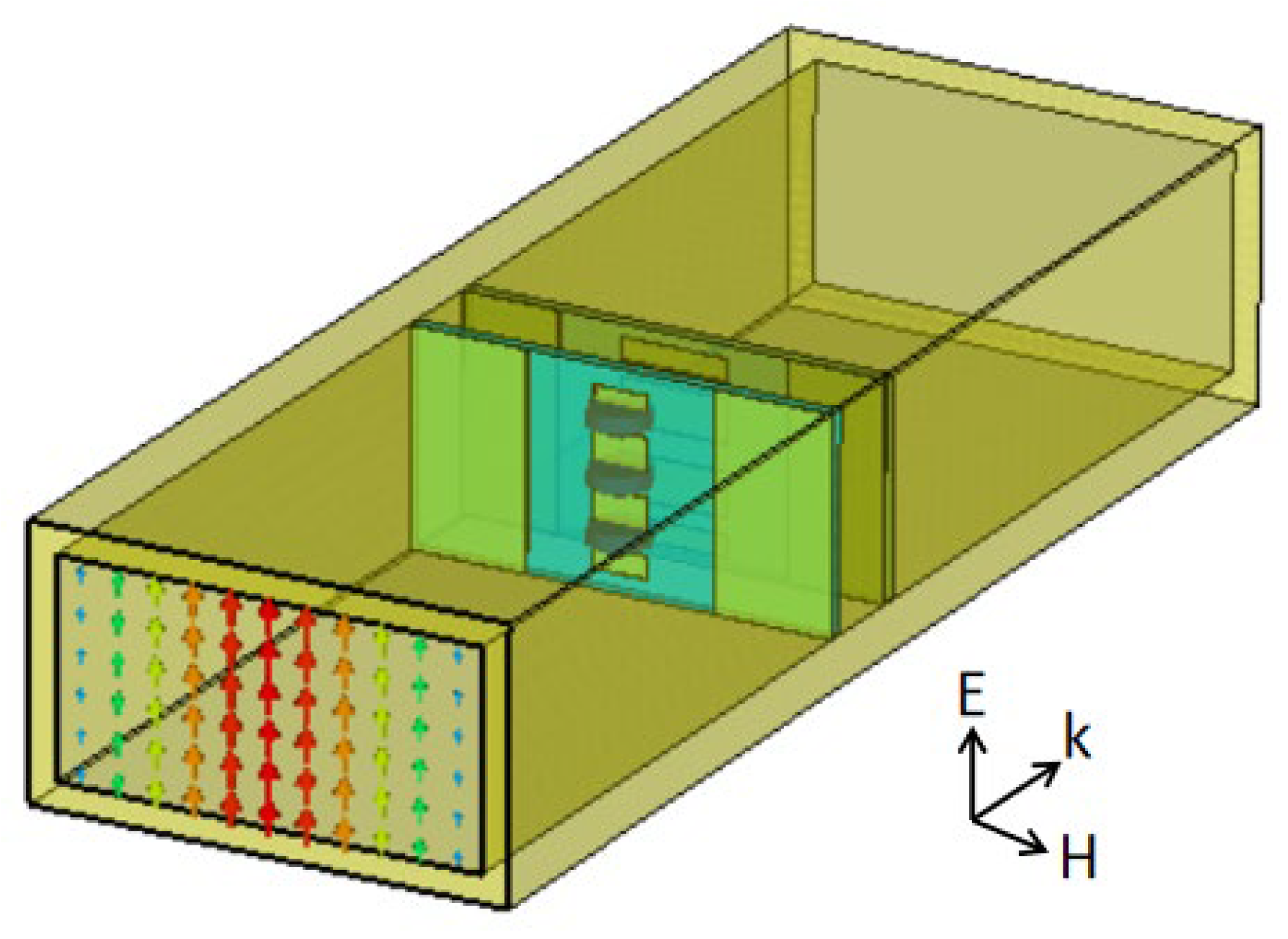
As shown in Figure 2, the structure depicted in Figure 1 is modeled in the full-wave simulation software CST Studio Suite 2024, and the model is positioned within a waveguide for full-wave simulation in the Ku band. The dimensions of the waveguide are referred to the standard waveguide WR62, with a width of 15.8 mm, a height of 7.9 mm, and a bandwidth from 12 to 18 GHz. To ensure consistency with the subsequent experimental environment, the waveguide walls and metal materials are set as perfect electric conductors (PECs), the interior of the waveguide is vacuum, and the substrate material is set as FR-4. Additionally, following comprehensive consideration of PIN diode parameters such as junction capacitance and ON-state resistance, the model MA4AGFCP910 was selected.
Figure 2.
Simulation model schematic of the proposed device.
In the simulations, lumped element values are employed to model the PIN diodes. Under the condition of low-power incident signals, the diodes are in OFF-state, and the equivalent capacitance Ce is set to 0.02 PF. While at the condition of relatively high-power incident signals, diodes are in ON-state, and the equivalent resistance R is set to 5.2 Ω.
3. Results and Discussion
3.1. Simulation Results and Discussion
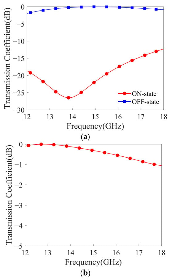
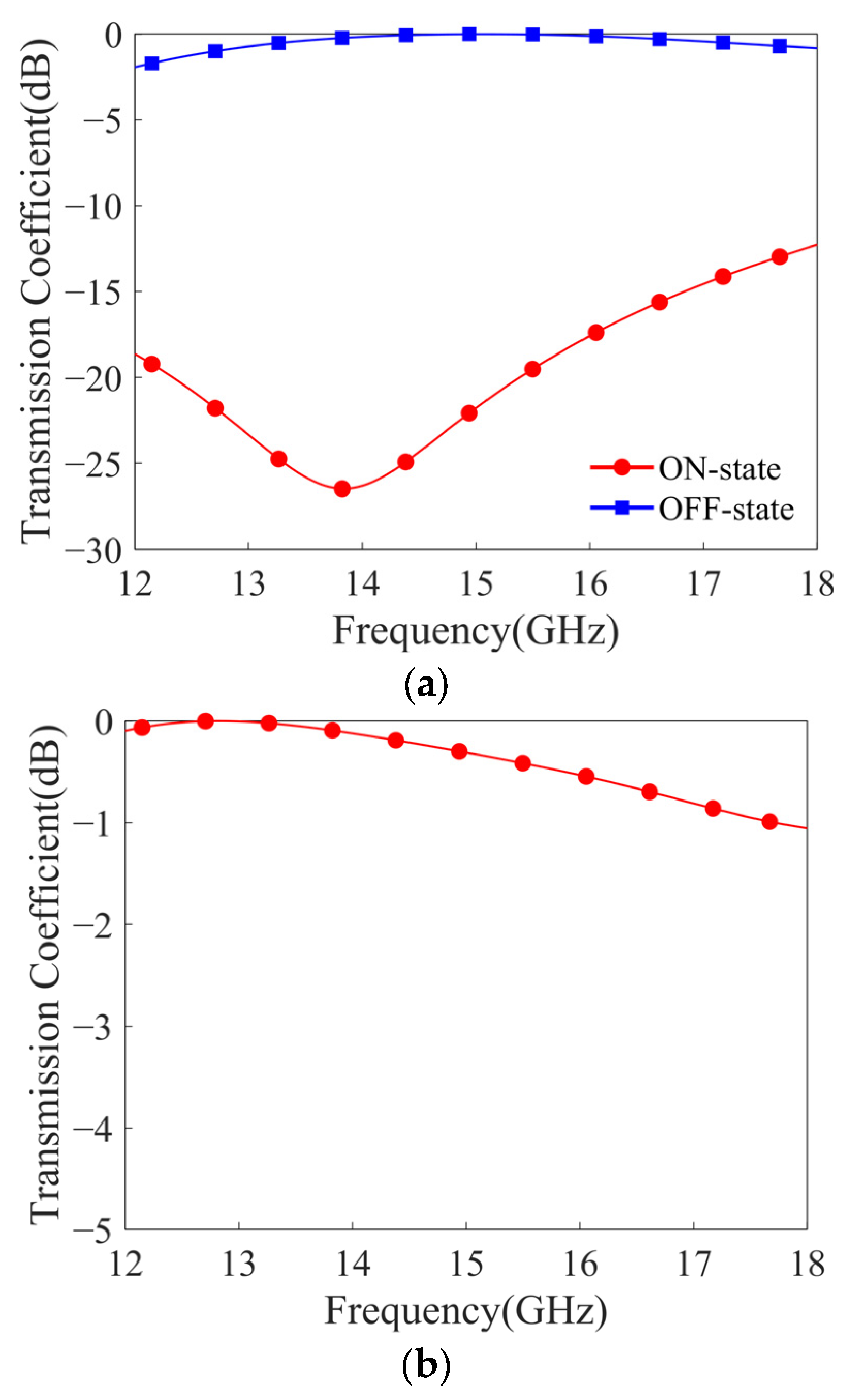
Figure 3a shows the simulated transmission coefficient of the first layer of the proposed device under different diode states. Under low-power signal incidence, the structure exhibits low-loss transmission characteristics across the 12–18 GHz band, but its IL performance degrades at the lower frequencies. Under high-power signal incidence, the SE exceeds 12 dB across the Ku band. While this single layer shows good IL in certain frequency ranges, its 1 dB IL bandwidth still does not cover the entire Ku band. Furthermore, the abovementioned simulations are based on ideal conditions and do not include parasitic effects introduced by the PIN diode packaging. Such effects, especially at higher frequencies, may further degrade the actual IL performance. To improve the overall performance and extend the operating bandwidth, a second layer is designed and combined with the first layer to form a dual-layer structure. As shown in Figure 3b, the second layer exhibits favorable low IL characteristics in the lower-frequency band. By properly designing the electromagnetic coupling between the two layers, the overall impedance matching can be optimized, thereby enabling effective protection over a wider frequency range.
Figure 3.
Simulated performance of the layer structures. (a) Transmission coefficients of the first layer under different diode operating states. (b) Transmission coefficient of the second layer.
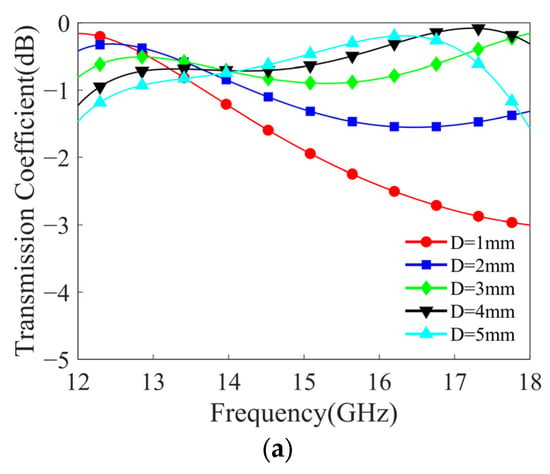
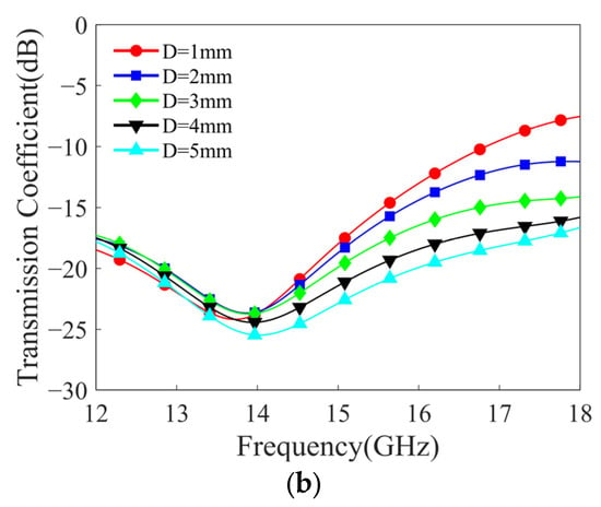
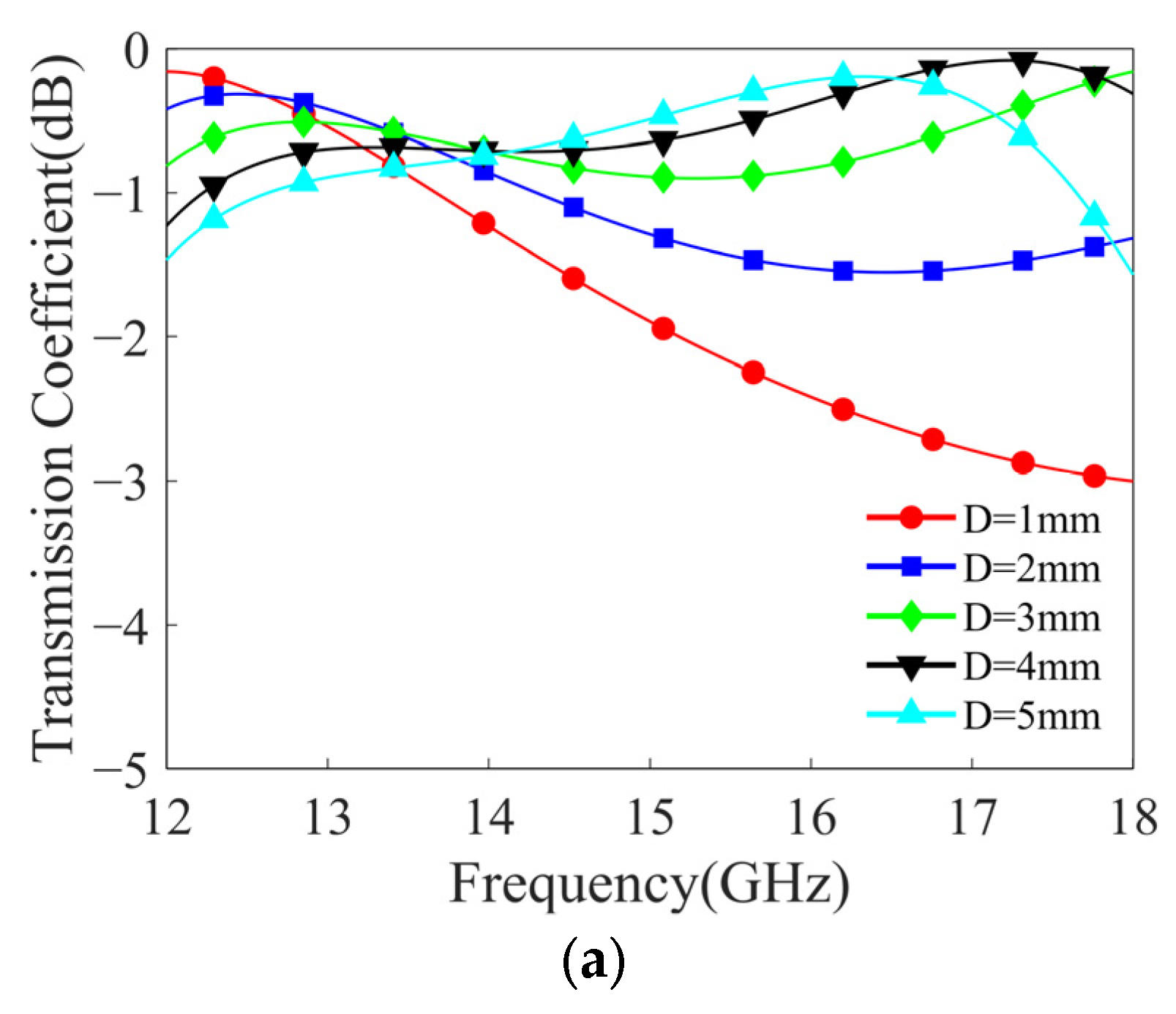
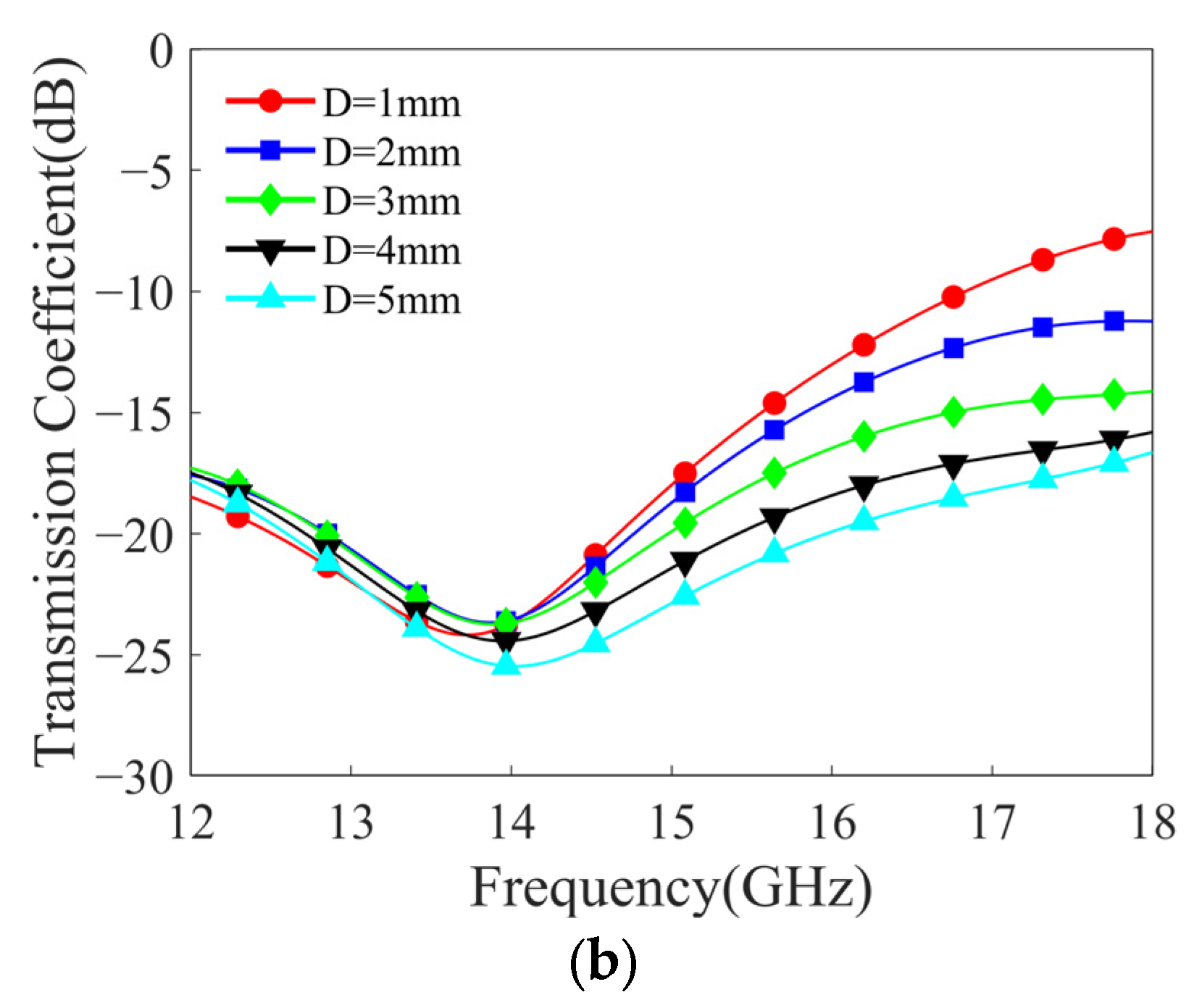
The inter-layer spacing D is a critical parameter that affects the coupling effect between the two layers. To carry out the structural coupling analysis, the two layers are placed parallel along the waveguide axis with the spacing D, as shown in the model diagram of Figure 2. Based on CST software, the influence of D varying from 1 mm to 5 mm on the transmission coefficient under different diode operating states is analyzed, and the results are given in Figure 4. Figure 4a shows the simulated IL versus the inter-layer spacing D. The variation in D significantly changes the distribution of resonance points. Specifically, as D gradually increases, the resonance points in the lower-frequency band shift only slightly, while those in the higher-frequency band gradually move toward lower frequencies. Figure 4b shows the simulated SE versus D. It can be observed that the variation in D has little influence on the SE, because this performance is mainly determined by the first layer itself. When D = 3 mm, the IL of the dual-layer structure remains below 1 dB across the entire Ku band, and its performance is significantly better than that of the single-layer structure. Therefore, in order to achieve good low-loss transmission characteristics over the whole Ku band, the inter-layer spacing D is finally set to 3 mm.
Figure 4.
Simulated transmission coefficient versus inter-layer spacing D under different diode states. (a) IL (OFF-state). (b) SE (ON-state).
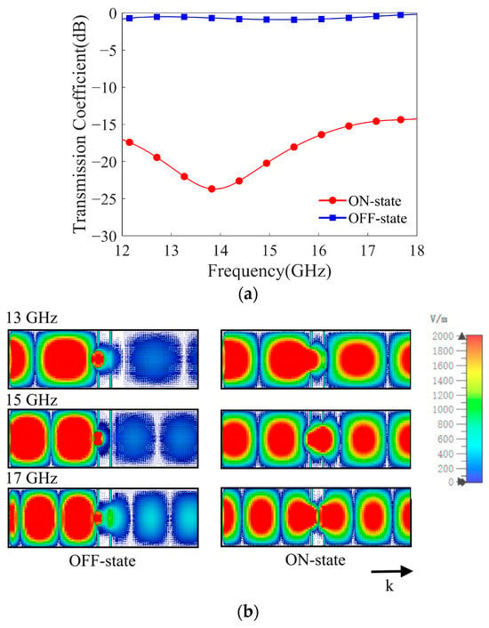
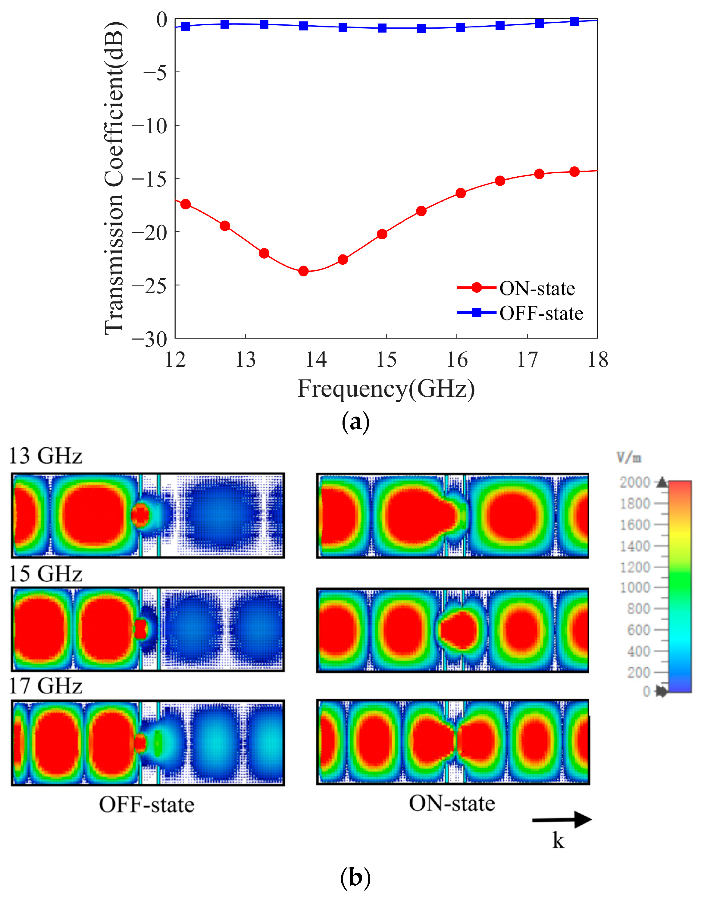
Figure 5a shows the simulated transmission coefficient of the waveguide energy-selective device under different diode states. Under low-power signal incidence, the IL is maintained below 1 dB across the Ku band. Under high-power signal incidence, the SE exceeds 14 dB across the Ku band and reaches 23.7 dB at 13.8 GHz. This demonstrates that the waveguide energy-selective device can achieve adaptive protection within the Ku band according to the power level of the incident signal.
Figure 5.
Simulated performance of the proposed device. (a) Transmission coefficients under different diode operating states. (b) Electric field distribution in the waveguide at 13, 15, and 17 GHz.
As shown in Figure 5b, further simulation was performed using CST to characterize the electric field transmission within the waveguide WR62. At frequencies of 13, 15, and 17 GHz, the low-power signals exhibit minimal attenuation when passing through the device, thus validating its low IL transmission capability. However, the electric field intensity of high-power signals is significantly reduced after passing through the device, thus validating its high-efficiency isolation capability. Furthermore, similar electric field distributions are observed at other frequency points, and thus no further elaboration will be provided here. In conclusion, the simulation results validate the capability of the device to achieve adaptive high-power electromagnetic isolation within the Ku band.
3.2. Experimental Results and Discussion
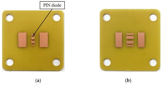
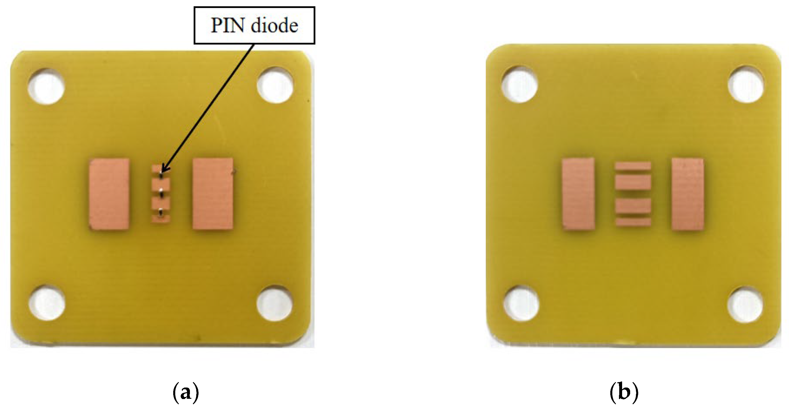
To validate the performance of the proposed device, a prototype was fabricated on a 0.5 mm thick FR-4 substrate, which is shown in Figure 6. The inter-layer spacing D between the two structures is 3 mm. Accordingly, a low-permittivity foam spacer with a thickness of 3 mm was utilized to meet this spacing requirement. The assembled device was then positioned at the flange interface between two sections of waveguide WR62 for experimental testing.
Figure 6.
Prototype of the proposed device. (a) Structure of the first layer. (b) Structure of the second layer.
3.2.1. Low-Power Measurement
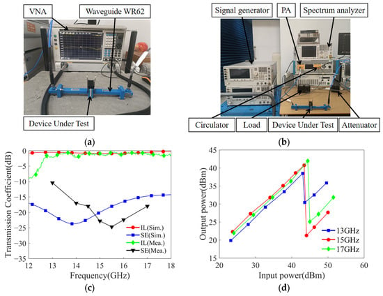
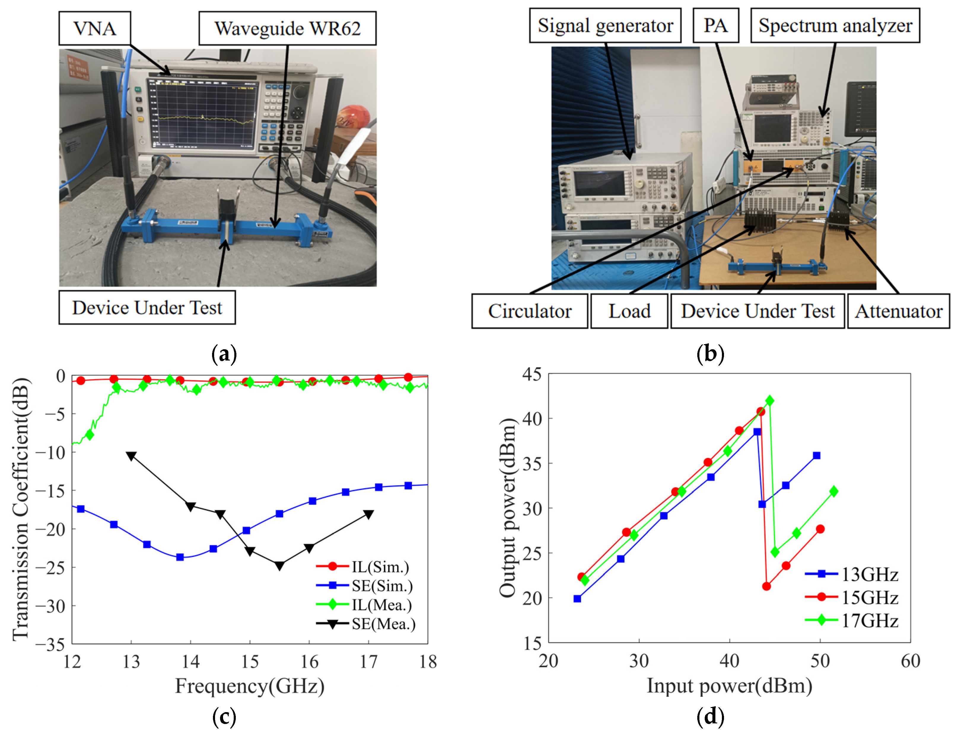
The measurement scheme under low-power signals incidence is depicted in Figure 7a, primarily consisting of a vector network analyzer (VNA) and a rectangular waveguide WR62. During the measurement, signals from VNA were fed into the waveguide, then propagated through the waveguide energy-selective device, and finally returned to the VNA via a transmission line. Furthermore, the output power of the VNA was set to −10 dBm, which is insufficient to turn on the diodes. Under this condition, the transmission curve measured by the VNA is recorded as the IL.
Figure 7.
Testing setup and experimental and simulation results of the prototype. (a) IL testing setup in waveguide. (b) SE testing setup in waveguide. (c) Measured and simulated IL and SE. (d) Output power of the device at 13 GHz, 15 GHz, and 17 GHz versus incident power.
The measured and simulated IL curves are illustrated in Figure 7c. The measured IL fluctuated around 1 dB within the 13–17 GHz band, indicating relatively minor signal attenuation. Compared to the simulation results, the measured IL is higher and exhibits noticeable fluctuations. The degradation in IL performance is attributed to two main factors: inevitable errors introduced during the fabrication and welding processes, and limitations of the simulation methodology. Specifically, the simulation in this work employed static lumped parameters to model the PIN diodes, whereas the actual equivalent parameters exhibit variations with frequency.
3.2.2. High-Power Measurement
The measurement scheme under high-power signals incidence is depicted in Figure 7b, primarily comprising instruments such as a signal generator, a power amplifier (PA), and a spectrum analyzer. During the measurement, signals generated by the signal generator are amplified by the PA, fed into the waveguide to interact with the energy-selective device, and then passed through an attenuator to the spectrum analyzer. Furthermore, to obtain the power attenuation at each test frequency, the measured results with the device under test loaded must be calibrated by comparing them with the unloaded case. The resulting calibrated power attenuation is recorded as the SE.
To verify the adaptive protection functionality of the waveguide energy-selective device, the relationship between the output power and the injected waveguide power was measured at three frequencies, namely 13 GHz, 15 GHz, and 17 GHz, as shown in Figure 7d. When the injected power is insufficient to turn on the PIN diodes, the output power increases linearly with the injected power, exhibiting low transmission loss. However, when the injected power reaches and slightly exceeds the protection threshold of the device, the operating state of the PIN diodes undergoes an abrupt transition. The response time of this process is on the nanosecond scale, manifesting as a rapid switch from the OFF-state to the ON-state, which is presented in the transmission characteristics as a sharp drop in output power. Experimental data indicate that the turn-on threshold of the device is approximately 44 dBm, with slight variations at different frequency points. This is attributed to differences in the voltage and current induced in the metal structure at different frequencies, which, in turn, affect the injected power level required for the PIN diodes to switch operating states. The fast, nonlinear response observed near the specific power threshold further verifies that the proposed device can achieve adaptive protection based on the power level of the incident signal.
Then, seven frequency points were selected at specified intervals across the 13–17 GHz band, and the relationship between SE and frequency was measured under an injected power of 45 dBm, as depicted in Figure 7c. Across the 13–17 GHz frequency band, the SE is measured to be above 10 dB, with a maximum of 24.7 dB at 15.5 GHz. The observed frequency shift in resonance points relative to simulation results can be attributed to three main factors. Firstly, the ideal lumped-element model used in the simulation fails to fully account for the parasitic inductances and capacitances introduced by the PIN diode packaging, which can significantly alter the resonant characteristics of the structure at high frequencies. Secondly, minor dimensional deviations introduced during fabrication and soldering modify the distributed capacitance and inductance of the structure, thereby affecting its actual frequency response. Thirdly, the dielectric constant of the FR-4 substrate was assigned a fixed value in the simulation, whereas the actual material exhibits dispersion, a phenomenon that becomes particularly pronounced in the high-frequency and further contributes to the discrepancies between measured and simulated results. Despite the discrepancies between experimental and simulation results, the favorable adaptive broadband-protective performance of the proposed device is sufficiently demonstrated by the measurements.
Since current research on ESSs operating in the Ku band remains relatively limited, Table 2 compares the main performance indicators of the proposed waveguide energy-selective device with those of existing high-performance and ultra-wideband ESSs, in order to evaluate its performance objectively. The comparison results indicate that the performance achieved by the proposed device in the Ku band, in terms of bandwidth, IL, and SE, is comparable to that of existing high-performance and ultra-wideband ESSs. This demonstrates that the proposed device effectively addresses common challenges in high-frequency design, such as limited bandwidth and increased IL. Thus, it provides a useful implementation and design reference for the broadband adaptive protection of sensitive electronic equipment in high-frequency applications.
Table 2.
Comparison of the proposed device with other ESSs.
4. Conclusions
A waveguide energy-selective device operating in the Ku band is presented in this paper, which autonomously switches its operating state according to incident power levels to ensure normal operation of backend sensitive components. To achieve broadband protection, a dual-layer structure was designed, and its inter-layer electromagnetic coupling effect was optimized. Subsequently, its transmission coefficient and field distribution characteristics under different diode operating states were analyzed. Finally, experimental tests were conducted based on a waveguide. A low IL fluctuating around 1 dB for low-power signals and a high SE no less than 10 dB for high-power signals are demonstrated by the experimental results. The effective broadband adaptive high-power protection capability of the proposed device is demonstrated by both the simulation and experimental results, revealing its promising application prospects in high-frequency and broadband protection fields.
Author Contributions
Conceptualization, T.L. and C.L.; methodology, T.L. and C.L.; validation, T.L. and Y.C.; formal analysis, T.L.; investigation, T.L. and Y.C.; resources, Y.X. and C.L.; data curation, T.L. and Y.C.; writing—original draft preparation, T.L.; writing—review and editing, Y.X. and C.L.; visualization, T.L.; supervision, C.L.; project administration, C.L.; funding acquisition, Y.X. and C.L. All authors have read and agreed to the published version of the manuscript.
Funding
This research was funded by the National Natural Science Foundation of China, grant number 62571533 and 62293491.
Data Availability Statement
The data presented in this study are available from the corresponding author upon reasonable request.
Conflicts of Interest
The authors declare no conflicts of interest.
Abbreviations
The following abbreviations are used in this manuscript:
| IL | Insertion loss |
| SE | Shielding effectiveness |
| FSSs | Frequency-selective surfaces |
| ESS | Energy-selective surface |
| PECs | Perfect electric conductors |
| VNA | Vector network analyzer |
| PA | Power amplifier |
References
- Benford, J. History and Future of High Power Microwaves. IEEE Trans. Plasma Sci. 2024, 52, 1137–1144. [Google Scholar] [CrossRef] [Scilit]
- Jia, L.; Wang, Y.; Song, Y.; Cui, W.; Chen, Z.; Wang, R.; Liu, Y.; Zhang, W.; Bao, M. The Detection Technology of High-Power Microwave: A Review. IEEE Trans. Instrum. Meas. 2024, 73, 1503620. [Google Scholar] [CrossRef] [Scilit]
- Radasky, W.A.; Baum, C.E.; Wik, M.W. Introduction to the special issue on high-power electromagnetics (HPEM) and intentional electromagnetic interference (IEMI). IEEE Trans. Electromagn. Compat. 2004, 46, 314–321. [Google Scholar] [CrossRef] [Scilit]
- Nitsch, D.; Camp, M.; Sabath, F.; Haseborg, J.L.; Garbe, H. Susceptibility of some electronic equipment to HPEM threats. IEEE Trans. Electromagn. Compat. 2004, 46, 380–389. [Google Scholar] [CrossRef]
- Gao, Q.; Wang, Y.E. A compact circuit model for frequency-selective limiters with strong field nonuniformity. In Proceedings of the 2023 IEEE Radio and Wireless Symposium (RWS), Las Vegas, NV, USA, 22–25 January 2023. [Google Scholar] [CrossRef] [Scilit]
- Li, S.; Ma, L.; Wang, L.; Lei, X.; Wu, B.; Cheng, G.J.; Liu, F. High power 10–18 GHz monolithic limiter based on GaAs p-i-n technology. IEEE Microw. Wirel. Compon. Lett. 2022, 32, 1107–1110. [Google Scholar] [CrossRef] [Scilit]
- Zhao, R.; Kang, X.; Zheng, Y.; Wu, H.; Wei, N.; Deng, S.; Wei, K.; Liu, X. High-power microwave limiters using recess-free AlGaN/GaNSchottky barrier diodes. IEEE Microw. Wirel. Technol. Lett. 2023, 33, 208–211. [Google Scholar] [CrossRef] [Scilit]
- Yang, P.; Zhou, W. Design and Experiment of Reduced-Dimension Adaptive Array Based on FIR Filters. IEEE Antennas Wirel. Propag. Lett. 2021, 20, 204–208. [Google Scholar] [CrossRef] [Scilit]
- Li, Y.; Gómez-García, R. High-order quasi-elliptic-type single ended and balanced wideband bandpass filters using microstrip-to microstrip vertical transitions. IEEE Trans. Circuits Syst. II Express Briefs 2023, 70, 1425–1429. [Google Scholar] [CrossRef] [Scilit]
- Munk, B.A. Frequency Selective Surfaces: Theory and Design; Wiley-Interscience Imprint: Hoboken, NJ, USA, 2000. [Google Scholar]
- Liu, N.; Sheng, X.; Zhang, C.; Fan, J.; Guo, D. A design method for synthesizing wideband band-stop FSS via its equivalent circuit model. IEEE Antennas Wirel. Propag. Lett. 2017, 16, 2721–2725. [Google Scholar] [CrossRef] [Scilit]
- Afzal, W.; Ebrahimi, A.; Robel, M.R.; Rowe, W.S.T. Low-profile higher-order narrowband bandpass miniaturized-element frequency selective surface. IEEE Trans. Antennas Propag. 2023, 71, 3736–3740. [Google Scholar] [CrossRef] [Scilit]
- Yang, S.; Zhang, F.; Song, L.; Zhang, F. Frequency-Selective Surface with Dual Polarization and Ultrawide Passband. IEEE Trans. Antennas Propag. 2025, 73, 2510–2520. [Google Scholar] [CrossRef] [Scilit]
- Yang, C.; Liu, P.; Huang, X. A novel method of energy selective surface for adaptive HPM/EMP protection. IEEE Antennas Wirel. Propag. Lett. 2013, 12, 112–115. [Google Scholar] [CrossRef] [Scilit]
- Gong, W.; Zhang, W.; Chen, X.; Han, G.; Han, L.; Su, J. A Low-Profile Energy Selective Surface with Ultra-Wide Absorption Band. IEEE Trans. Microw. Theory Tech. 2023, 71, 1348–1355. [Google Scholar] [CrossRef] [Scilit]
- Wu, Z.; Xu, Y.; Liu, P.; Tian, T.; Lin, M. An ultra-broadband energy selective surface design method: From filter circuits to metamaterials. IEEE Trans. Antennas Propag. 2023, 71, 5865–5873. [Google Scholar] [CrossRef] [Scilit]
- Xia, R.; Ren, J.; Xue, Z. A Tunable Ultra-Broadband Energy Selective Surface Design. In Proceedings of the 2024 IEEE 7th Information Technology, Networking, Electronic and Automation Control Conference, Chongqing, China, 15–17 March 2024. [Google Scholar]
- Hu, N.; Wang, K.; Zhang, J.; Zha, S.; Wu, Z.; Liu, C.; Liu, P. Design of Ultrawideband Energy-Selective Surface for High-Power Microwave Protection. IEEE Antennas Wirel. Propag. Lett. 2019, 18, 669–673. [Google Scholar] [CrossRef] [Scilit]
- Zhou, L.; Liu, L.; Shen, Z. High-performance energy selective surface based on the double-resonance concept. IEEE Trans. Antennas Propag. 2021, 69, 7658–7666. [Google Scholar] [CrossRef] [Scilit]
- Jiang, H.; Deng, B.; Zha, S.; Tian, T.; Liu, P. Energy Selective Structure with High Shielding Efficiency Based on Slotline. IEEE Microw. Wirel. Technol. Lett. 2025, 35, 1182–1185. [Google Scholar] [CrossRef] [Scilit]
- Hu, N.; Zhao, Y.; Zhang, J.; Liu, P.; Xu, H.; Costa, F. Highperformance energy selective surface based on equivalent circuit design approach. IEEE Trans. Antennas Propag. 2022, 70, 4526–4538. [Google Scholar] [CrossRef] [Scilit]
- Zhou, T.; Liu, P.; Liu, C.; Jiang, H.; Tian, T. Multilayer Energy Selective Surface with Wide Operational Band and High Shielding Effectiveness Based on Second-Order Filter. IEEE Trans. Electromagn. Compat. 2024, 67, 337–340. [Google Scholar] [CrossRef] [Scilit]
- Wu, Z.; Liu, P.; Deng, B.; Tian, T.; Zha, S.; Ni, X. An Ultrabroadband Energy Selective Surface with Nonreciprocal Performance for HIRF Protection. IEEE Trans. Electromagn. Compat. 2023, 65, 1202–1210. [Google Scholar] [CrossRef] [Scilit]
- Liu, C.; Xu, Y.; Liu, H.; Ma, H. Self-activated nonreciprocal transmission isolation via absorption-asymmetry-triggered directional phase transition in VO2-based terahertz metamaterials. J. Mater. Chem. C 2025, 13, 20313–20792. [Google Scholar] [CrossRef] [Scilit]
- Yang, Y.; Vaseem, M.; Wang, R.; Makki, B.; Shamim, A. A Fully Screen-Printed Vanadium-Dioxide Switch-Based Wideband Reconfigurable Intelligent Surface for 5G and Beyond. IEEE Trans. Microw. Theory Tech. 2025, 73, 5979–5991. [Google Scholar] [CrossRef] [Scilit]
- Chen, Q.; Cheng, Y.; Min, W.; Xiao, Y.; Xia, Z. A composite energy-selective surface based on diode-induced VO2 conduction for the applications of adaptive electromagnetic protection. Microw. Opt. Technol. Lett. 2023, 66, e33895. [Google Scholar] [CrossRef] [Scilit]
- Chen, L.; Wang, J.; Liu, X.; Feng, D.; Sun, G. A Flexible Range-Doppler Modulation Method for Pulse-Doppler Radar Using Phase-Switched Screen. IEEE Trans. Antennas Propag. 2025, 73, 6774–6787. [Google Scholar] [CrossRef] [Scilit]
- Gudkova, N.; Shnitnikov, A. Millimeter-wave waveguide dioide limiter. In Proceedings of the 2006 16th International Crimean Microwave and Telecommunication Technology, Sevastopol, Ukraine, 11–15 September 2006. [Google Scholar] [CrossRef] [Scilit]
- Miligy, A.F.; Elfeky, A.H.; Kheirallah, H.N.; Rizk, M.R.M.; Madany, Y.M. Study of Miniaturized SIW and RWG Limiters for S-Band Receiver Protector Radar and Communication Applications. Prog. Electromagn. Res. C 2023, 132, 171–185. [Google Scholar] [CrossRef] [Scilit]
- Park, J.-S.; Son, H.-W.; Choi, J.-Y.; Kim, B.-M. Application of transmission-resonant aperture to the waveguide limiter design. In Proceedings of the 2013 Asia-Pacific Microwave Conference Proceedings, Seoul, Republic of Korea, 5–8 November 2013. [Google Scholar]
- Helszajn, J.; Murray, R.W.; Davidson, E.G.S.; Suttie, R.A. Waveguide subsidiary resonance ferrite limiters. IEEE Trans. Microw. Theory Tech. 1977, 25, 190–196. [Google Scholar] [CrossRef] [Scilit]
- Wang, L.; Tang, Z.; Bao, H.; Ding, D. An Electromagnetic-Plasma Fluid Model Simulation of Waveguide Plasma Limiter Filled with Different Easily Ionized Inert Gas. IEEE Trans. Plasma Sci. 2022, 50, 3839–3847. [Google Scholar] [CrossRef] [Scilit]
- Zhang, J.; Hu, N.; Wu, Z.; Deng, B.; Lin, M.; Ding, L.; Liu, P. Adaptive high-impedance surface for prevention of waveguide’s high-intensity wave. IEEE Trans. Antennas Propag. 2021, 69, 7679–7687. [Google Scholar] [CrossRef] [Scilit]
- Huang, R.; Liu, J.; Liu, C.; Hu, N.; Zha, S. Self-Switchable Broadband Waveguide Protector Against High Power Microwave. IEEE Trans. Electromagn. Compat. 2023, 65, 355–359. [Google Scholar] [CrossRef] [Scilit]
- Wu, Z.; Lin, M.; Zhang, J.; Liu, J. Energy selective filter with powerdependent transmission effectiveness in waveguide. Electronics 2019, 8, 236. [Google Scholar] [CrossRef] [Scilit]
- Huang, R.; Liu, J.; Liu, C.; Xu, Y.; Zha, S. A Broadband Adaptive Waveguide High-Power Microwave Protector. IEEE Microw. Wirel. Compon. Lett. 2023, 33, 15–18. [Google Scholar] [CrossRef] [Scilit]
- Zhang, J.; Lin, M.; Wu, Z.; Ding, L.; Bian, L.; Liu, P. Energy Selective Surface with Power-Dependent Transmission Coefficient for High-Power Microwave Protection in Waveguide. IEEE Trans. Antennas Propag. 2019, 67, 2494–2502. [Google Scholar] [CrossRef] [Scilit]
- Wu, Z.; Lin, M.; Liu, J.; Zhang, J. Waveguide Energy-Selection-Filter Switch Array. IEEE Access 2019, 7, 67686–67694. [Google Scholar] [CrossRef] [Scilit]

Disclaimer/Publisher’s Note: The statements, opinions and data contained in all publications are solely those of the individual author(s) and contributor(s) and not of MDPI and/or the editor(s). MDPI and/or the editor(s) disclaim responsibility for any injury to people or property resulting from any ideas, methods, instructions or products referred to in the content. |
© 2026 by the authors. Licensee MDPI, Basel, Switzerland. This article is an open access article distributed under the terms and conditions of the Creative Commons Attribution (CC BY) license.