Abstract
With the rapid development of artificial intelligence (AI) and machine learning (ML) applications, wafer-level optical I/O is becoming increasingly attractive for massive and efficient data interconnects in future wafer-scale multi-processor-units (multi-XPU) compute clusters with unparalleled data bandwidth, energy efficiency, and low latency. In this paper, we present a 300 mm sized wafer reticle-stitched low-pressure chemical vapor deposition (LPCVD) silicon nitride (SiN) waveguide technology and demonstrate a multi-reticle-stitched ~56 cm long waveguides across 20 reticles with propagation loss of 0.13~0.15 dB/cm at 1310 nm wavelength, and <0.001~0.002 dB SiN waveguide stitch loss, which is because of <5 nm high-precision reticle lithography offset. These advantageous features of low-loss reticle-stitched SiN waveguides have the potential to significantly enhance future optically interconnected wafer-scale multi-chip compute systems.
1. Introduction
The increasing popularity of artificial intelligence (AI) and machine learning (ML) is driving a growing demand for high-bandwidth, low-latency, and energy-efficient interconnects between compute chips (such as CPUs, GPUs, …, XPUs, etc.) and high-bandwidth memory (HBM) in AI/ML compute clusters [1,2,3,4]. Wafer-level optical interconnects (WL-OIs) is an emerging technology to interconnect multiple tens of XPUs or HBMs on a single 300 mm wafer [5,6]. This technology offers superior chip edge bandwidth density, energy efficiency, and latency compared to fiber-coupled links while also providing significantly longer reach than on-wafer copper interconnects [7,8]. As interconnect distances in the envisioned WL-OIs compute clusters (see Figure 1) are expected to span tens of centimeters, there is a strong need for developing low-loss, high-confinement, low-crosstalk, and high-density waveguide arrays that can propagate across the entire 300 mm wafer to exceed the current limits of edge bandwidth density.
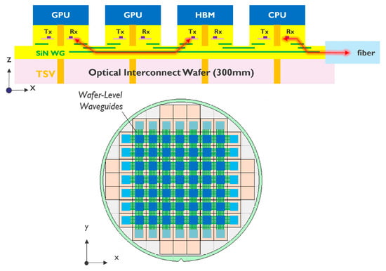
Figure 1.
Envisioned optically interconnected compute system on a 300 mm sized optical interconnect wafer. Instead of optical fiber array or copper, high-density and low-loss reticle-stitched SiN waveguides (green) enabling extremely high edge bandwidth density and high energy-efficiency wafer-level optical I/O. CPU: central processing unit. GPU: graphic processing unit. HBM: high-bandwidth memory. Tx: optical transmitter. Rx: optical receiver. TSV: through-silicon via.
Compared to silicon-based (refractive index n~3.5) waveguides [9], silicon reticle-stitched waveguides offer higher optical confinement but come with higher cost, higher propagation loss, and greater sensitivity to reticle offset. The SiN reticle stitch is preferred due to its lower sidewall-scattering-induced propagation loss and lower mode-mismatch-induced stitch loss because of its moderate refractive index (refractive index n~2.0) [10,11]. SiN is also considered convenient in silicon photonic integration. Therefore, in this paper, we present a 300 mm wafer-scale low-pressure chemical vapor deposition (LPCVD) SiN waveguide with high-precision reticle-stitch lithography. Cross-wafer-stitched (up to 20 reticles) waveguides up to 56 cm long are demonstrated with waveguide propagation loss of 0.12~0.15 dB/cm at 1310 nm.
2. Prospects of High-Precision Reticle Stitching
Reticle stitching is mature and commercially available for most silicon photonic applications on 200 mm platforms with a typical 100~200 nm reticle offset. However, for future bandwidth-hungry wafer-level optical I/O, ~10 nm level or higher precision reticle stitching is critical for bandwidth-intensive wafer-level optical I/O targeting > Tbit/s/mm chip edge bandwidth density. Below Table 1 is the detailed discussion on the importance of ~10 nm level high precision for future wafer-level optical I/O.

Table 1.
Prospects of high-precision reticle stitching.
3. Multi-Reticle-Stitched SiN Waveguides
To experimentally demonstrate the multi-reticle-stitched waveguides, test vehicle wafers (total of eight wafers for statistics, in which wafers D1~D4 are with 300 nm thick SiN, and wafers D5~D8 are with 400 nm thick SiN) were implemented in imec’s 300 mm CMOS pilot line [12]. Test vehicle wafers (in Figure 2a) are simple with only one patterned SiN layer. The 300 mm sized wafer processing starts with a 2.7 µm thick buried oxide (BOX) deposition. Next, either a 300 or 400 nm thick LPCVD SiN layer is deposited. Both 300 nm and 400 nm thicknesses are commonly used in silicon photonic integration with high optical confinement. The 300 nm thick SiN waveguides are expected to exhibit less sidewall scattering and lower propagation loss, while the 400 nm thick SiN waveguides have a higher effective index, allowing for larger bend curvatures and denser waveguide arrays [13]. After lithography and SiN patterning, an oxide top cladding layer is deposited and subsequently planarized, targeting a >2 µm thick top oxide (TOX) on SiN. The LPCVD SiN layer is patterned using advanced 193 nm immersion lithography, leveraging the high alignment precision for reticle stitch. Two different reticles (as shown in Figure 2c), each covering a full 26 × 33 mm2 SiN mask, are used to form wafer-scale reticle-stitched waveguides. Each mask is exposed with the chosen reticles through a dedicated lithography job, resulting in the complete wafermap exposure depicted in Figure 2b.
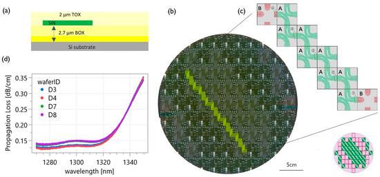
Figure 2.
Multi-reticle-stitched SiN waveguide. (a) Test vehicle wafers (total 8 wafers for statistics, wafers D1~D4 are with 300 nm thick SiN, wafers D5~D8 are with 400 nm thick SiN) to demonstrate the reticle-stitched SiN waveguides. (b) A dedicated full wafermap exposure is employed to form multi-reticle-stitched loopback waveguides (highlighted in yellow) by arranging lithography jobs using mask A and mask B. (c) The design principle of loopback waveguide bundles. (d) Multi-reticle-stitched waveguide propagation loss is extracted at 0.13~0.15 dB/cm at 1310 nm using a cutback technique.
Several cross-wafer loopback waveguides, up to 56 cm, are patterned by arranging the long waveguide bundles on the first SiN mask (Mask A) and the waveguide bend/termination (such as grating couplers and waveguide U-turns) on the second SiN mask (Mask B). Measuring cross-wafer waveguide loss is challenging on a wafer probe station due to the large wafer-scale separation between input and output grating coupler ports. To simplify the optical measurement process, loopback waveguides are employed. The design principle of the multi-reticle-stitched loopback waveguide is illustrated in Figure 2c. By probing optical fibers at different dies at ①~⑤ different wafer locations (in Figure 2c), the corresponding optical losses for the 8.3 cm, 20.2 cm, 32.1 cm, 44.1 cm, and 56.0 cm multi-reticle-stitched loopback waveguides can be measured. The propagation loss of the stitched waveguides can be extracted using the cutback technique (optical O-band optical loss readout shown in Figure 2d). The extracted propagation loss of the SiN waveguides is 0.13~0.15 dB/cm at 1310 nm. Additionally, the propagation loss slightly increases to higher loss at the longer 1350 nm wavelength due to impurities and chemical bond absorption (Si–H and N–H) inside the deposited SiN [14,15,16]. Although the propagation loss is slightly higher than the current state of the art (i.e., <0.1 dB/cm for SiN waveguides), the LPCVD SiN waveguides used in this work are integration-friendly, cost-effective, and commercially available, without requiring complex fabrication steps such as extremely high-temperature annealing.
4. SiN Waveguide Stitch Loss Analysis
Reticle offset, normally at the 10 nm or 100 nm level, is technically inevitable in stepper lithography, with the abrupt stitch interfaces and optical mode mismatch resulting in an additional waveguide stitch loss and unwanted interface reflection. At first, high-resolution scanning electron microscopy (SEM) is used to examine the etched interfaces of the stitched SiN waveguides. SEM images (in Figure 3) reveal a visually smooth interface without defects at the reticle-to-reticle interfaces. Then, dedicated double-exposed overlay (OVL) structures (inspection methodology shown in Figure 4) are used to analyze the reticle offset using SEM image processing and inspection function. OVL measurements were fully conducted on four wafers (each wafer has 53 reticles, and each reticle has six OVL structures at separate locations on the mask scribe line), and the measured x- or y- reticle offset was <5 nm.
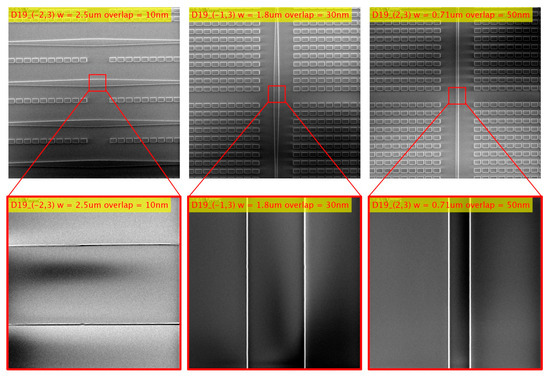
Figure 3.
SEM inspections of the reticle-to-reticle interfaces of the stitched SiN waveguides. (Stitch widths are optionally 0.71, 1.8, and 2.5 µm, expected stitch loss < 0.01 dB; see Appendix A Figure A1).
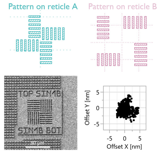
Figure 4.
To characterize the reticle-to-reticle lithography offset, each reticle contains 6 OVL inspection structures to measure the lithography offset in both x and y directions. The reticle offset readouts (4 wafers × 53 reticles × 6 OVL inspection marks) are all <5 nm.
Since reticle offset is inspected at less than 5 nm, to analyze the SiN waveguide stitch loss, the add–drop ring resonator pairs are proposed in Figure 5a. Ring resonators are preferred and widely used to monitor the SiN loss because they require very little chip area and are not sensitive to SiN grating coupler loss variations. Figure 5a shows the design layout of the add–drop ring resonator pair, including a reference ring resonator (ref ring, green) and a stitched ring resonator (stitch ring, partly red). Figure 5b is the schematic showing the design parameters, such as the input, thru, drop ports, self-coupling coefficients r1, r2, bus-to-ring distance, and SiN waveguide width, all labeled on the graph. All ring resonators are identically ~6 mm long with 50 µm radius waveguide bends. More importantly, the stitch ring has 12 additional reticle-to-reticle waveguide stitches to accumulate and amplify the weak stitch loss signal. Then, by comparing the internal loss differences between the stitch ring and ref ring, the average waveguide stitch loss can be determined. The calculated internal loss for both the stitch ring and reference ring across eight wafers, each with six randomly measured dies, is shown in Figure 6. As expected, the calculated internal loss of the stitch ring is generally higher than that of the reference ring (i.e., the red markers are expectedly higher than the green markers, with a few exceptions attributable to measurement deviations). This increased loss in stitch rings is attributed to 12 additional waveguide stitches. Then, the SiN waveguide mean stitch loss can be calculated by
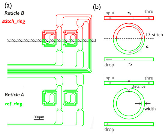
Figure 5.
SiN waveguide stitch loss extraction using compact ring resonators (in the case of vertical stitching, the horizontal stitching case is similar). (a) Add–drop ring resonator pair with identical ref ring and stitch ring resonator. The stitch ring has 12 additional stitches for precisely measuring the waveguide stitch loss. (b) The schematic of the add–drop ring resonator pair. The ring round-trip is ~6 mm long, bend radii are 50 µm, bus-to-ring distance is 1.6 µm. The ring resonators are designed in an undercoupled state, then the add–drop ring internal loss will closely approximate ring intrinsic loss; see Appendix A Figure A2. (The dashed line indicate the reticle scribe line).
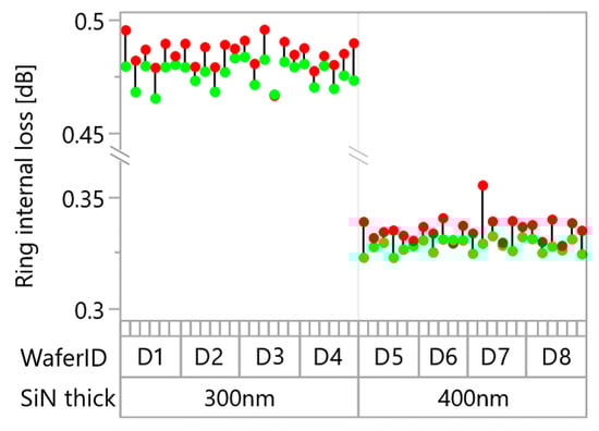
Figure 6.
Ring internal loss of the add–drop ring resonator pairs (measured 8 wafers × 6 dies). Red and green markers represent the stitch ring and ref ring internal loss, respectively. The loss differences are from the 12 additional waveguide stitches. The 300 nm thick ring resonators are measured to have higher internal loss because of the 50 µm radius sharp waveguide bends.
The extracted stitch loss is shown in Figure 7. Because of the <5 nm lithography reticle offset, the stitch loss is calculated to be <0.001~0.002 dB, which is comparable to a ~50 μm SiN waveguide section propagation loss. This result is promising for the future development and application of wafer-level optical interconnects.
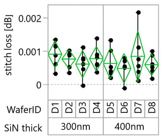
Figure 7.
SiN waveguide stitch loss is analyzed at <0.001~0.002 dB, which is comparable to a ~50 μm SiN waveguide section propagation loss. (8 wafers × 6 dies statistics; diamond plot showing the mean stitch loss range with a default 95% confidence interval).
5. Stitch Loss with a Worse 20 nm Reticle Offset
To validate the 0.001~0.002 dB stitch loss in Figure 7, a 20 nm y-direction reticle offset was imposed on D4 and D8 wafers by slightly offsetting the whole mask B lithography job. This was designed to see an expectedly higher waveguide stitch loss at the specific locations (the purple interfaces in Figure 8a). The overlay (OVL) inspection revealed that the reticle y-offset at the purple interfaces was increased to 20 ± 4 nm (mean ± 3σ). Then, the internal loss of the stitch ring and ref ring in wafers D4 and D8 was measured. For comparison, wafers D3 and D7 (without the 20 nm imposed y-offset) were also measured. Each wafer had more than 10 random dies measured at the purple interfaces. The results of the ring internal loss of the add–drop ring resonator pairs are presented in Figure 8c. The red markers are the internal loss of the stitch rings, the green markers are the internal loss of the ref rings, and the black bars are the internal loss difference between the stitch ring and ref ring. Obviously, wafers D4 and D8 showed higher stitch ring internal loss compared to wafers D3 and D7. Then, the increased SiN waveguide stitch loss can be calculated in Figure 8d; stitch loss increases to 0.002~0.005 dB due to the worse 20 nm y-offset. Notably, the 2.5 µm wide taper-up stitch exhibits ~0.001 dB lower loss compared to the 1.8 µm wide taper-up stitch. This indicates that a wider stitch width is better when the reticle offsets worsen.
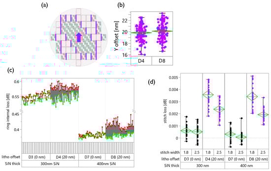
Figure 8.
Increased waveguide stitch loss due to 20 nm imposed reticle y-offset. (a) Imposed 20 nm y-offset at the specific locations (marked in purple) of mask-A-to-mask-B stitch interfaces by slightly offsetting the whole mask B lithography job. The purple arrow indicates the imposed reticle offset direction. (b) SEM inspected 20 ± 4 nm y-offset at the purple interfaces. (c) Red and green markers represent the stitch ring and ref ring internal loss, respectively. D4 and D8 have obviously higher stitch ring internal loss at the purple interfaces (compared to D3 and D7 reference wafers). (d) The SiN waveguide stitch loss increases to 0.002~0.005 dB due to the 20 nm imposed offset. And the 2.5 µm wide taper-up stitch can be 0.001~0.002 dB lower optical loss than the 1.8 µm wide taper-up stitch. (Diamond plot showing the mean stitch loss with a default 95% confidence interval).
6. Conclusions
In this paper, we present a 300 mm sized wafer reticle-stitched SiN waveguide. By arranging a dedicated wafermap exposure, up to 56 cm long multi-reticle-stitched loopback waveguides are demonstrated, propagating across 20 reticle interfaces with a propagation loss of 0.12~0.15 dB/cm at 1310 nm. Although the SiN waveguide propagation loss is a bit higher than that of state-of-the-art research, these cross-wafer waveguides exhibit a very small reticle-to-reticle lithography offset of <5 nm and negligible stitch loss of <0.001~0.002 dB. By leveraging the demonstrated reticle-stitched low-loss SiN waveguide, the future wafer-scale multi-XPU compute systems can be envisioned with unparalleled interconnect bandwidth, energy efficiency, and latency, which are essential for advancing wafer-level optical interconnects beyond state-of-the-art technologies in AI/ML compute clusters.
Author Contributions
Software, validation, formal analysis, investigation, writing—original draft preparation, writing—review and editing, and visualization by P.X.; methodology (mask preparation and support) by L.H. and D.T.; methodology (wafer processing) by C.M., G.L. and N.G.; methodology (lithography, metrology) by R.V.E., A.M. (Andrea Mingardi) and J.V.O.; data curation by R.M.; resources by P.V., M.C., D.V. and A.M. (Andy Miller); conceptualization, supervision, and project administration and funding acquisition by Y.B., F.F. and J.V.C. All authors have read and agreed to the published version of the manuscript.
Funding
This work was supported by imec’s industry affiliation R&D program on “Optical I/O”.
Institutional Review Board Statement
Not applicable; this study did not involve humans or animals.
Informed Consent Statement
Not applicable; this study did not involve humans or animals.
Data Availability Statement
The original contributions presented in this study are included in the article. Further inquiries can be directed to the corresponding authors.
Acknowledgments
The authors thank imec’s APPM (Advanced Patterning, Process & Materials) team for their support.
Conflicts of Interest
The authors declare no conflict of interest.
Appendix A
Appendix A.1. Summary on SiN SiN Technology
Table A1.
Summaries of the LPCVD SiN technology.
Table A1.
Summaries of the LPCVD SiN technology.
| Category | Value (±3σ) |
|---|---|
| Mask Reticle | Mask Size = 26 × 33 mm Reticle offset < 5 nm Lithography = ASML TWINSCAN NXT:2000i DUV from ASML, Veldhoven, The Netherlands |
| LPCVD SiN deposition recipe | LPCVD deposition Temperature = 770 °C LPCVD Pressure = 225 mTorr DCS (dichlorosilane, SiH2Cl2) gas flow = 80 sccm NH3 (ammonia) gas flow = 280 sccm |
| Fourier-transform infrared (FTIR) spectrum of LPCVD SiN |  A slight peak (inset) at approximately 3300 cm−1 in the FTIR spectrum (red) of an LPCVD SiN film indicates the presence of N–H (nitrogen-hydrogen) bonds. |
| SiN ring resonator design parameters (layout in Figure 5) | Ring length = 6011 µm Number of 50 µm radius 90-degree bends = 26 Number of waveguide stitches = 12 Bus-to-ring distance = 1.5, 1.6 µm |
| 300 nm thick SiN waveguide | Actual thickness: 302.1 ± 11.3 nm Waveguide loss: 0.131 ± 0.005 dB/cm 50 µm radius 90-degree bend loss: 0.0159 ± 0.0057 dB Ref ring internal loss = 0.485 ± 0.0762 dB (d = 1.5 µm) Ref ring internal loss = 0.475 ± 0.0816 dB (d = 1.6 µm) Stitch loss = 0.00076 ± 0.0010 dB |
| 400 nm thick SiN waveguide | Actual thickness: 401.2 ± 15.6 nm Waveguide loss: 0.145 ± 0.004 dB/cm 50 µm radius 90-degree bend loss: 0.0087 ± 0.0045 dB Ref ring internal loss = 0.349 ± 0.0783 dB (d = 1.5 µm) Ref ring internal loss = 0.315 ± 0.0846 dB (d = 1.6 µm) Stitch loss = 0.00064 ± 0.0014 dB |
Appendix A.2. Loss Simulation on SiN Waveguide Stitch
In the paper, plain stitch and taper-up stitch (in Figure A1) are proposed for demonstrating the reticle-stitched waveguide and for investigating the waveguide stitch loss. As a reference design, plain stitch is simple and has relatively low risk, with a SiN waveguide stitch at a single-mode waveguide width (commonly 710 nm wide) without waveguide taper or multimode sections. So, there is no risk of high-order mode excitation loss due to unexpected fabrication defects. On the other hand, the taper-up stitch is a promising alternative that tapers up to a wider waveguide width to mitigate the mode mismatch at the reticle-to-reticle interface.
Figure A1 is the 3D-FDTD simulations, in which a worst-case 20 nm reticle lithography offset (in y-direction) is considered, the simulated optical field (electromagnetic wave electric field y-component) is shown in Figure A1b, and the simulated insertion loss and return loss, i.e., the waveguide back reflectance from reticle-to-reticle stitch interface, are shown in Figure A1c. For plain stitch, the interface is <0.01 dB waveguide stitch loss, and the return loss is >50 dB, while for taper-up stitch (for example, SiN waveguide adiabatically tapered up to a 1.8 µm wide multimode section), the simulated interface is expected to have better optical loss (~0.006 dB insertion loss and >60 dB return loss) because of the enlarged mode field diameter and less mode mismatch.

Figure A1.
SiN waveguide stitch structures. (a) Schematic of stitched SiN waveguide at the reticle-to-reticle interface. Key parameters are shown, e.g., lithography overlap (assumed 10~50 nm, to well-pattern the waveguide against the ten-nanometer-level reticle offset), reticle offset (typically ten-nanometer-level offset due to displacement), and stitch width (SiN waveguide optionally tapering up to either 1.8 µm wide or 2.5 µm wide from a plain 0.71 µm wide SiN waveguide by using adiabatic tapers). (b) Simulated optical field at a worst-case scenario 20 nm reticle offset in the y-direction. (c) Simulated insertion loss and return loss of the plain stitch and 1.8 µm wide taper-up stitch.
Appendix A.3. Stitch Loss Extraction Method
Ring resonators are preferred and widely used to monitor SiN loss because they require very little chip area. These ring resonators are generally in an undercoupled state, i.e., the bus-to-ring distances are relatively large to ensure the add–drop ring internal loss closely approximates ring intrinsic loss (see Figure 5). In this work, a 1.6 µm bus-to-ring distance stitch ring and ref ring resonators are used to numerically analyze the SiN waveguide stitch loss. Although the ring resonator design parameters—such as the ~6 mm round-trip length, 50 µm bend radius, etc.—influence the measured ring internal loss, for example, longer round-trip propagation, sharper waveguide bending, and smaller bus-to-ring distances can result in a higher internal loss readout. However, the stitch ring and ref rings have identical layouts; the stitch loss is the internal loss difference between the stitch ring and the ref ring, which are totally independent of the add–drop ring design parameters (for details, see Table A2).

Figure A2.
Typical spectra with 10 nm spectral span of an add–drop ring resonator, from which the ring mean internal loss can be numerically analyzed. The resonance wavelength dips are marked and analyzed.
The typical measured spectra (input-to-thru and input-to-drop) of the add–drop ring resonator are shown in Figure A1. In this work, spectra spanning 10 nm (centered at 1310 nm optical O-band) are measured using a tunable laser source with an instrument resolution of 1 picometer. The mean internal loss of the ring resonator is calculated from all resonant wavelengths within this 10 nm span, as this method yields more accurate ring internal loss results given the limited 1 pm spectral resolution. From these spectra, the FSR (free spectral range), FWHM (full width at half maximum), Tmax (maximum power percentage of input-to-drop transmission), and Rmin (minimum power percentage of input-to-thru transmission) can be extracted. Then, the round-trip internal loss of the ring resonator can be numerically calculated by the following equations [17,18]:
in which a is the internal round-trip loss coefficient of the ring resonator. The parameters r1 and r2 are the self-coupling coefficients of the bus-to-ring coupling. In this case, r1 = r2 because of the symmetrical coupling structures.
Table A2.
Ring internal loss analysis and discussion (stitch ring vs. ref ring).
Table A2.
Ring internal loss analysis and discussion (stitch ring vs. ref ring).
| # | Components of Ring Internal Loss | Stitch Ring | Ref Ring | Remarks | Discussion |
|---|---|---|---|---|---|
| 1 | Dielectric material absorption loss | √ | √ | identical loss | Although the ring resonator design influences the readout of internal loss, the stitch ring and ref ring share an identical layout, ensuring that their intrinsic losses are the same. |
| 2 | Round-trip propagation loss | √ | √ | ||
| 3 | Waveguide bending loss | √ | √ | ||
| 4 | Coupling loss | √ | √ | Although smaller bus-to-ring distances would result in slightly higher coupling loss, the stitch ring and reference ring have identical layouts, ensuring that the coupling loss is the same. | |
| 5 | Waveguide stitch loss | √ | × | loss difference | The stitch loss is the internal loss difference between the stitch ring and the ref ring, which is independent of the add–drop ring design parameters. |
| √ indicates the resonator has this loss; × indicates the resonator does not have this loss. | |||||
References
- Liu, H.; Urata, R.; Yasumura, K.; Zhou, X.; Bannon, R.; Berger, J.; Dashti, P.; Jouppi, N.; Lam, C.; Li, S.; et al. Lightwave fabrics: At-scale optical circuit switching for datacenter and machine learning systems. In Proceedings of the ACM SIGCOMM 2023 Conference, New York, NY, USA, 10–14 September 2023. [Google Scholar]
- Khani, M.; Ghobadi, M.; Alizadeh, M.; Zhu, Z.; Glick, M.; Bergman, K.; Vahdat, A.; Klenk, B.; Ebrahimi, E. SiP-ML: High-bandwidth optical network interconnects for machine learning training. In Proceedings of the ACM SIGCOMM 2021 Conference, New York, NY, USA, 23–27 August 2021. [Google Scholar]
- Young, I.A.; Mohammed, E.; Liao, J.T.; Kern, A.M.; Palermo, S.; Block, B.A.; Reshotko, M.R.; Chang, P.L. Optical I/O technology for tera-scale computing. IEEE J. Solid-State Circuits 2010, 45, 235–248. [Google Scholar] [CrossRef]
- Gholami, A.; Yao, Z.; Kim, S.; Hooper, C.; Mahoney, M.W.; Keutzer, K. AI and memory wall. IEEE Micro 2024, 44, 33–39. [Google Scholar] [CrossRef]
- Xu, P.; He, J.; Kennes, K.; Dvoretskii, A.; Podpod, A.; Lepage, G.; Golshani, N.; Magdziak, R.; Bipul, S.; Bode, D.; et al. Collective die-to-wafer bonding enabling low-loss evanescent coupling for optically interconnected system-on-wafer. In Proceedings of the 2024 Optical Fiber Communications Conference and Exhibition (OFC), San Diego, CA, USA, 24–28 March 2024. [Google Scholar]
- Kennes, K.; Dvoretskii, A.; Podpod, A.; Xu, P.; He, J.; Lepage, G.; Golshani, N.; Verheyen, P.; Magdziak, R.; Bipul, S.; et al. Collective die-to-wafer assembly process for optically interconnected system-on-wafer. In Proceedings of the IEEE 74th Electronic Components and Technology Conference (ECTC), Denver, CO, USA, 28–31 May 2024. [Google Scholar]
- Pal, S.; Petrisko, D.; Tomei, M.; Gupta, P.; Iyer, S.S.; Kumar, R. Architecting waferscale processors—A GPU case study. In Proceedings of the 2019 IEEE International Symposium on High Performance Computer Architecture (HPCA), Washington, DC, USA, 16–20 February 2019. [Google Scholar]
- Zhang, Y.; Shang, K.; Zhang, Y.; Li, S.; Lin, Y.C.; Yoo, S.B. Low-loss and broadband wafer-scale optical interposers for large-scale heterogeneous integration. Opt. Express 2024, 32, 40–51. [Google Scholar] [CrossRef]
- Seok, T.J.; Kwon, K.; Henriksson, J.; Luo, J.; Wu, M.C. Wafer-scale silicon photonic switches beyond die size limit. Optica 2019, 6, 490–494. [Google Scholar] [CrossRef]
- Liu, J.; Huang, G.; Wang, R.N.; He, J.; Raja, A.S.; Liu, T.; Engelsen, N.J.; Kippenberg, T.J. High-yield, wafer-scale fabrication of ultralow-loss, dispersion-engineered silicon nitride photonic circuits. Nat. Commun. 2021, 12, 2236. [Google Scholar] [CrossRef]
- Isichenko, A.; Chauhan, N.; Bose, D.; Wang, J.; Kunz, P.D.; Blumenthal, D.J. Photonic integrated beam delivery for a rubidium 3D magneto-optical trap. Nat. Commun. 2023, 14, 3080. [Google Scholar] [CrossRef] [PubMed]
- Ferraro, F.J.; De Heyn, P.; Kim, M.; Rajasekaran, N.; Berciano, M.; Muliuk, G.; Bode, D.; Lepage, G.; Janssen, S.; Magdziak, R.; et al. Imec silicon photonics platforms: Performance overview and roadmap. In Proceedings of the Next-Generation Optical Communication: Components, Sub-Systems, and Systems XII, San Francisco, CA, USA, 15 March 2023. [Google Scholar]
- Jin, W.; Feshali, A.; Paniccia, M.; Bowers, J.E. Seamless multi-reticle photonics. Opt. Lett. 2021, 46, 2984–2987. [Google Scholar] [CrossRef] [PubMed]
- Golshani, N.; Witters, T.; McGurk, J.; De Heyn, P.; De Coster, J.; Milenin, A.; Thiam, A.; Mingardi, A.; Verheyen, P.; Pantouvaki, M.; et al. Low-loss, low-temperature PVD sin waveguides. In Proceedings of the 2021 IEEE 17th International Conference on Group IV Photonics (GFP), Málaga, Spain, 7–10 December 2021. [Google Scholar]
- Wang, L.; Xie, W.; Van Thourhout, D.; Zhang, Y.; Yu, H.; Wang, S. Nonlinear silicon nitride waveguides based on a PECVD deposition platform. Opt. Express 2018, 26, 9645–9654. [Google Scholar] [CrossRef] [PubMed]
- Shao, Z.; Chen, Y.; Chen, H.; Zhang, Y.; Zhang, F.; Jian, J.; Fan, Z.; Liu, L.; Yang, C.; Zhou, L.; et al. Ultra-low temperature silicon nitride photonic integration platform. Opt. Express 2016, 24, 1865–1872. [Google Scholar] [CrossRef]
- Bogaerts, W.; De Heyn, P.; Van Vaerenbergh, T.; De Vos, K.; Kumar Selvaraja, S.; Claes, T.; Dumon, P.; Bienstman, P.; Van Thourhout, D.; Baets, R. Silicon microring resonators. Laser Photonics Rev. 2012, 6, 47–73. [Google Scholar] [CrossRef]
- Deng, Q.; Liu, L.; Li, X.; Michel, J.; Zhou, Z. Linear-regression-based approach for loss extraction from ring resonators. Opt. Lett. 2016, 41, 4747–4750. [Google Scholar] [CrossRef] [PubMed]


Disclaimer/Publisher’s Note: The statements, opinions and data contained in all publications are solely those of the individual author(s) and contributor(s) and not of MDPI and/or the editor(s). MDPI and/or the editor(s) disclaim responsibility for any injury to people or property resulting from any ideas, methods, instructions or products referred to in the content. |
© 2026 by the authors. Licensee MDPI, Basel, Switzerland. This article is an open access article distributed under the terms and conditions of the Creative Commons Attribution (CC BY) license.