


Abstract
The continuous scaling of microelectronic technology nodes has imposed fundamental physical constraints on conventional floating-gate (FG) non-volatile memory, driving the adoption of charge-trapping memory such as Silicon–Oxide–Nitride–Oxide–Silicon (SONOS) technology. SONOS devices offer advantages in scalability, endurance, and compatibility with advanced CMOS processes, yet their high-temperature reliability remains challenging due to charge loss mechanisms influenced by device structure and material properties. In this work, we systematically evaluate the reliability of two-transistor SONOS memory fabricated using a 28 nm high-K metal gate (HKMG) process. A refined temperature-dependent charge loss model (T-model) is introduced, which, by incorporating a characteristic temperature parameter (T0) that captures the dynamic shift in activation energy, fundamentally departs from the constant-activation energy assumption of the conventional Arrhenius model. This approach more accurately describes charge retention behavior across a wide temperature range. Experimental results demonstrate excellent device performance, including endurance exceeding 104 program/erase cycles at 85 °C and data retention over 10 years at 85 °C. The T-model shows strong agreement with measured data, providing a physically grounded framework for predicting long-term reliability. This study not only validated a novel charge loss model, providing insights for predicting the failure time of SONOS memory, but also demonstrated that HKMG-integrated SONOS memory exhibits high reliability.
1. Introduction
With the rapid advancement of electronic devices and the accelerated push toward digitalization, global data generation is experiencing exponential growth, while the diversification of data types and the unpredictability of data scale present numerous challenges for data storage technologies [1,2,3]. Memory technology plays a crucial role in the modern information society [4]. As a non-volatile storage solution, flash memory serves as a fundamental component in electronic systems such as smartphones, embedded storage solutions, and data centers [5,6]. The continuous scaling of microelectronic technology nodes is imposing fundamental physical constraints upon traditional non-volatile memory devices such as floating gate (FG) memory, whose internal structures are becoming increasingly susceptible to reliability degradation [7,8]. Furthermore, as dimensions shrink, the coupling coefficient between floating gates and control gates continuously decreases. Simultaneously, the distance between storage cells within the array becomes increasingly shorter, leading to a growing crosstalk issue between adjacent floating gate memory cells. This further limits the application of traditional floating gate memory in high-density storage [9]. In non-volatile memory research, reliability testing is crucial for assessing charge retention performance, which underpins long-term data stability. Charge retention capability depends on electron leakage from the charge trapping layer—a property influenced by device structure, dielectric materials, and temperature [10,11,12]. Silicon–Oxide–Nitride–Oxide–Silicon (SONOS) memory, which utilizes localized charge trapping in silicon nitride instead of a conventional floating gate, offers advantages such as reduced parasitic coupling effects, superior stress-induced leakage current (SILC) immunity, improved endurance and compatibility with advanced CMOS processes [13,14,15,16]. Additionally, the charge capture layer in SONOS memory disperses stored charge, thereby eliminating capacitive coupling interference from adjacent storage cells and addressing reliability issues caused by charge concentration in traditional floating gate structures [11,17]. These fundamental advantages have accelerated its adoption in embedded applications ranging from microcontrollers to Internet of Things (IoT) devices, where reliability, power efficiency, and integration density are paramount. The SONOS device features a planar structure comprising substrate silicon, tunnel oxide (TO), silicon nitride charge trapping layer (CTL), and blocking oxide (BO) [18,19]. The TO enables charge tunneling, the CTL provides nonvolatile charge storage, and the BO ensures data retention. Replacing the conventional gate dielectric with an Oxide–Nitride–Oxide (ONO) stack not only simplifies fabrication but also enhances memory performance and reliability, offering a promising alternative to floating gate memory architectures [16,20,21,22]. However, its high-temperature reliability remains challenging due to the lower electron affinity of silicon nitride and the use of ultrathin tunnel oxide, which promote charge loss through reverse tunneling toward the substrate or gate [23,24]. This introduces a fundamental trade-off between data retention and Fowler–Nordheim (FN) tunneling-based program/erase (P/E) speed. To enhance SONOS reliability without compromising write efficiency, it is essential to improve the effectiveness of highly accelerated life testing widely employed in production monitoring. This, in turn, critically depends on the establishment of accurate extrapolation models derived from a deeper physical understanding of the underlying failure mechanisms.
In recent years, researchers have proposed various models to describe the charge loss mechanisms and temperature-dependent data retention characteristics of both floating gate and SONOS-type non-volatile memories [25]. Conventionally, the Arrhenius model (1/T-model) has been widely employed to characterize the temperature dependence of charge retention time (τR). Its expression is given by [26]
where Ea denotes the activation energy (eV), representing the minimum energy barrier that charge carriers must overcome to escape from trap states or tunnel through dielectric barriers, T is the absolute testing temperature (K), kB is the Boltzmann constant, and τ0 is a fitting time parameter (s). However, experimental data collected over a temperature range of 90 °C to 430 °C reveal that the activation energy is not constant but varies between 0.3 eV and 1.9 eV, significantly deviating from the predictions of the Arrhenius law [25,27,28]. This discrepancy highlights the limitations of the conventional model in accurately describing charge loss behavior in both FG and SONOS devices. To address this issue, De Salvo et al. proposed an alternative T-model with the following equations [29,30]:
where T0 represents a characteristic temperature in Kelvin, and F denotes the electric field strength in MV/cm across the tunnel oxide. Based on the physical mechanisms of charge transport through the tunneling oxide and ONO stack, this T-model provides a better fit to experimental data reported across multiple studies, covering a broad range of temperatures and activation energies. Although the charge loss mechanisms in SONOS devices differ from those in FG memories, primarily involving trap-assisted tunneling and thermal excitation rather than Fowler–Nordheim (FN) tunneling, the T-model remains effective in predicting the data retention behavior of SONOS devices. For SONOS-type memories, the equivalent activation energy can be derived as [31]
It is evident that the T-model, by incorporating the characteristic temperature T0, offers a more accurate description of charge loss in both FG and SONOS devices across extended temperature ranges. It also provides new insights into the underlying charge transport mechanisms. Notably, although the T-model has been primarily validated on devices fabricated using conventional processes, its applicability and predictive accuracy in advanced high-k metal gate (HKMG) technology remain largely unexplored. Therefore, this study experimentally validated the T-model using SONOS memory devices fabricated using a 28 nm HKMG process, thereby confirming the model’s applicability at advanced technology nodes. This establishes a crucial experimental foundation for its future application in scaling non-volatile memory design and reliability assessment. Nevertheless, the physical basis for the excellent fit of the T-model to SONOS device behavior requires further investigation. Future research should focus on elucidating the impact of device structure on charge loss dynamics to support the design of more reliable non-volatile memory technologies.
This work presents a systematic investigation of the reliability characteristics of two-transistor (2T) SONOS memory fabricated in 28 nm high-k metal gate (HKMG) technology and investigates the influence of the T-model on charge retention performance by conducting electrical characterization of fabricated SONOS memory devices under various temperatures. The experimental results are fitted and compared with the T-model to validate its accuracy and physical rationality. Furthermore, reliability tests are performed on the HKMG SONOS memory cells, and the corresponding results are analyzed in detail. Through rigorous experimental analysis and modeling, we demonstrate excellent endurance (>104 P/E cycles at 85 °C) and data retention (>10 years at 85 °C) capabilities, validated using a refined T-model that shows close agreement with empirical data across multiple charge loss criteria. The findings of this work not only provide new insights into the charge leakage mechanisms in SONOS memories but also offer deeper understanding and practical guidance for reliability evaluation and performance assessment of such devices. Additionally, this study establishes a scientific basis for optimizing memory design and enhancing device reliability.
2. Materials and Methods
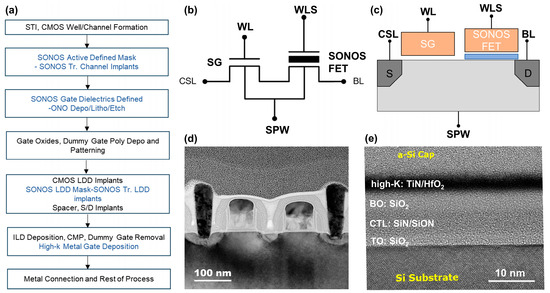
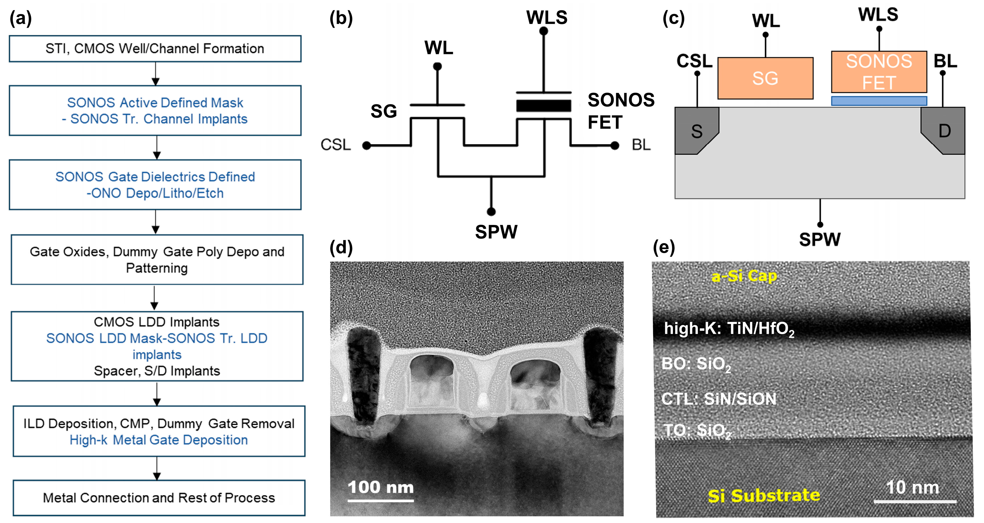
This work has fabricated SONOS memory devices with a two-transistor structure (2T), comprising a selected gate (SG) and a SONOS field-effect transistor (SONOS FET). The integration of SONOS non-volatile memory into a HKMG CMOS process is illustrated in Figure 1a. Key SONOS-specific modules are inserted after well and channel implantation but prior to logic gate oxidation. A dedicated mask defines the SONOS active region and enables tailored channel implants. An additional mask opens a window for deposition of the Oxide–Nitride–Oxide (ONO) stack, which is subsequently patterned to form the SONOS gate dielectric and removed from CMOS regions. The ONO layer was grown in situ using low-pressure chemical vapor deposition (LPCVD). Specifically, the tunnel oxide layer was deposited at 780 °C to a thickness of 2 nm, the charge trap layer was grown at 760 °C to 6 nm, and the barrier oxide layer was formed at 740 °C to a thickness of 3.5 nm. Following gate oxide growth, a dummy polysilicon gate is deposited and patterned. After CMOS lightly doped drain (LDD) implantation, a SONOS-specific mask enables customized LDD implantation for the memory device. Spacer formation and source/drain implantation are then performed. The process continues with interlayer dielectric (ILD) deposition, chemical mechanical polishing (CMP), dummy gate removal, and replacement with a high-k metal gate. The high-k layers of TiN and HfO2 were grown using atomic layer deposition (ALD). Finally, back-end-of-line metallization and interconnect formation complete the device fabrication. Subsequently, a semiconductor analyzer (Keysight B1500A) was used to measure the electrical characteristics of the SONOS memory for experimental validation. The test primarily focuses on evaluating the programming and soft programming threshold voltage of SONOS memory. During testing, a small voltage is applied to the drain (bit line), while all other device terminals are biased at 0 V. The threshold voltage is determined as the gate voltage required to turn on the memory cell.
Figure 1.
(a) SONOS memory manufacturing flowchart; (b) 2T SONOS memory unit circuit diagram; (c) 2T SONOS memory unit structure diagram; (d) 2T SONOS memory unit structure TEM image; (e) cross section TEM image of SONOS FET’s ONO stack.
3. Results and Discussion
Figure 1b and Figure 1c respectively illustrate the circuit schematic and device model of the two-transistor (2T) SONOS memory cell, which consists of a select gate (SG) transistor and a SONOS field effect transistor (FET). The SG controls the switching operation of the memory cell, while the SONOS FET is responsible for data storage. As shown, the drain of the SG is connected to the source of the SONOS FET. A sufficiently high gate voltage applied to the SG turns on the memory cell, enabling read, program, or erase operations. Both program and erase operations rely on Fowler-Nordheim tunneling under a uniform vertical electric field, differing only in the polarity of the applied gate voltage. Programming applies a positive gate bias to inject electrons from the substrate into the charge-trapping layer, whereas erasing uses a negative gate bias to extract the stored electrons back to the substrate, enabling bidirectional charge control through field-directed tunneling. To clearly reveal the structure of the fabricated 2T SONOS memory, cross-sectional TEM images of two adjacent memory cells on the same page are presented in Figure 1d. Furthermore, Figure 1e displays a high-resolution TEM image of the ONO stack within the SONOS FET. The gate stack employs a TiN/HfO2 high-k metal gate structure, with layer thicknesses of approximately 2 nm for the tunneling oxide, 6 nm for the charge-trapping nitride, 3.5 nm for the blocking oxide, and 3.5 nm for the high-k dielectric. Among these, the tunnel oxide influences direct tunneling and SILC. The charge-trapping layer affects charge trapping and release, while the blocking layer controls the electric field and long-term retention. Thus, ONO stack thickness and quality critically determine device reliability [32,33]. From the TEM images, it can be observed that the device exhibits uniform and flat material layers with clearly defined interfaces, thereby providing a certain assurance for the normal output of its electrical performance.
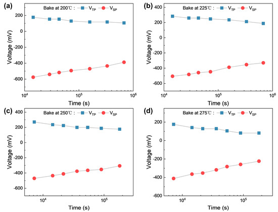
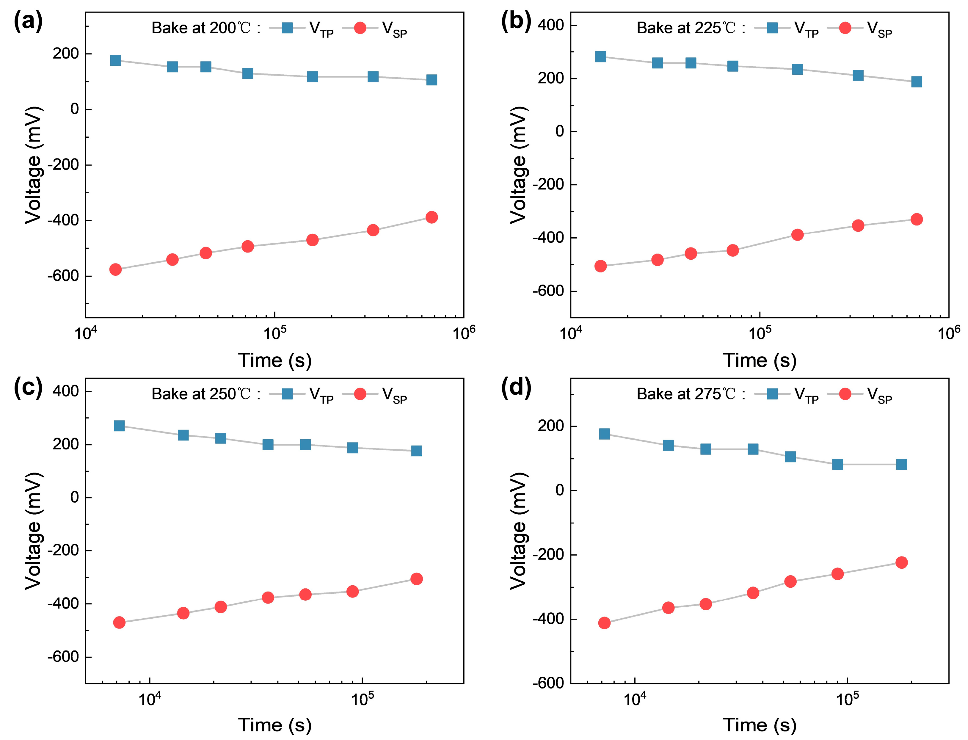
As illustrated in Figure 2a–d, the program/erase curves of SONOS devices were measured over the temperature ranges of 200 °C to 275 °C in 25 °C steps. The blue curve represents the programming threshold voltage (VTP), while the red curve denotes the soft programming threshold voltage (VSP). The soft programming phenomenon occurs when an erased memory cell elevates the threshold voltage of adjacent cells, thereby narrowing the threshold voltage window and resulting in a characteristic curve identical to that observed in the erased state. According to the results shown in the figure, the absolute value of the device’s VSP diminished over time regardless of whether it was in the programmed or erased state. For instance, at a baking time of 180,000 s, as the temperature increased, the VSP gradually increased from −460 mV to −380 mV, −305 mV, and finally −223 mV. Consequently, the storage window also decreased from 577 mV to 305 mV. This indicates that devices subjected to programming and erasing cycles will experience accelerated charge loss after a certain period. This occurs because during programming and erasing, high-energy electrons or holes continuously collide, disrupting the crystal structure of the interface and silicon dioxide layer. These collisions generate numerous interface states, leading to leakage of electrons stored within the charge trap layer [34,35,36].
Figure 2.
Threshold voltage shift in programming (ΔVTP) and soft programming (ΔVSP) state as a function of baking time under different temperatures: (a) 200 °C, (b) 225 °C, (c) 250 °C, and (d) 275 °C bake condition.
As introduced earlier, a novel method (the T-model) was proposed for evaluating charge loss behavior. In practice, this method operates by monitoring the rate of threshold voltage shift during baking. To validate the accuracy of the model in predicting device failure time, we conducted comprehensive reliability tests on SONOS devices, including endurance and data retention characteristics. Moreover, establishing a lifetime model as a function of temperature requires a well-defined failure criterion. Clearly, the more charge loss the memory cell can tolerate, the longer its lifetime will be. Charge loss (CL) is positively correlated with the offset of the threshold voltage window with the greater the reduction in the voltage window, the more significant the charge loss is. As can be seen from Figure 2, the variation in VSP is faster than that in VTP over time. This makes VSP a more sensitive metric for early charge loss, enabling earlier detection of device degradation. Consequently, lifetime predictions based on VSP drift yield more conservative estimates. Therefore, the relationship between the CL and VSP shift is more apparent: a larger deviation of the post-baking VSP from its typical value (VSP,TYPICAL) indicates a higher degree of charge loss. The relationship can be expressed as follows:
This criterion ensures a statistically robust margin for defining functional failure under operational stress conditions. According to Equation (5), when the actual VSP measured after device baking is 500 mV and the initial value VSP,TYPICAL is −750 mV, this corresponds to a charge loss of 33%.
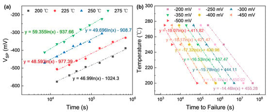
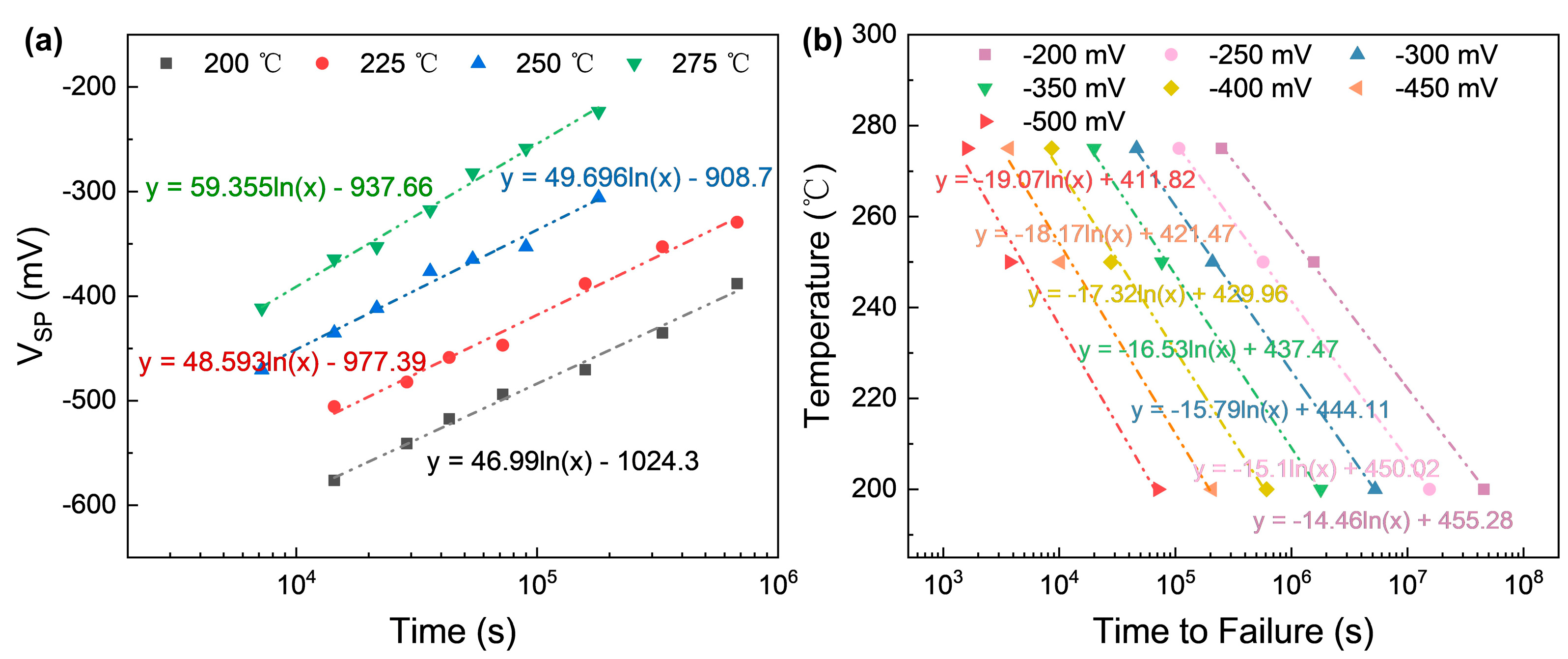
The influence of baking temperature on charge loss is significant. Elevated temperatures accelerate these processes, leading to more rapid charge loss. Systematic characterization across multiple temperature conditions provides critical insights into high-temperature reliability, enabling targeted improvements in device endurance and data retention. Subsequently, the soft program threshold voltage (VSP) shift was extracted from Figure 2a–d, revealing clear dependencies on both temperature and baking duration. To ensure assessment accuracy, extrapolation methods were employed to project the charge loss trends. From Figure 3a, with increasing baking temperature, the threshold voltage offset of the device increases, and the failure time progressively decreases. Additionally, the relationship between VSP and baking time at different temperatures was quantitatively described using fitted equations (displayed in Figure 3a), establishing a mathematical framework for predicting failure times under various operating conditions.
Figure 3.
(a) Fitting curves of VSP over time at different baking temperatures; (b) fitting curves for temperature versus time to failure under different failure VSP standards.
Furthermore, failure times corresponding to VSP criteria ranging from −500 mV to −200 mV were extracted from Figure 3a and comprehensively compared in Figure 3b. The experimental temperature–failure time data were fitted using the T-model formulation, with respective fitting equations displayed for each failure criterion. At 85 °C, the predicted lifetimes vary significantly with different failure thresholds: 0.9 years (−500 mV), 3.5 years (−450 mV), 14.2 years (−400 mV), 57.8 years (−350 mV), 239.0 years (−300 mV), 999.1 years (−250 mV), and 4190.4 years (−200 mV). This progression demonstrates consistent alignment with experimental observations, where elevated temperatures systematically accelerate charge dissipation. The comparative results highlight the critical sensitivity of lifetime predictions to the selected failure criterion, emphasizing the necessity of careful threshold selection in reliability modeling. The close agreement between theoretical predictions and empirical data validates the T-model’s applicability across multiple degradation levels and thermal conditions, providing a robust framework for optimizing SONOS memory performance in high-temperature applications.
The detailed model parameters calculated under different VSP conditions are summarized in Table 1. The coefficient for time in each fitted equation in Figure 3b is T0. As indicated in the table, as the failure VSP criteria increases, the corresponding charge loss in SONOS memory also continues to grow, whilst the characteristic T0 in the T-model progressively diminishes. It is noteworthy that the characteristic temperature T0 reaches 19.07 K at 33% charge loss, showing close alignment with the value of 21 K reported in the study by De Salto et al. [29]. The consistency between these results not only validates the accuracy of our model but also enhances its predictive credibility in capturing the underlying physical mechanisms. This alignment provides a reliable theoretical foundation for further research and device optimization.
Table 1.
T-model parameters for three charge loss conditions.
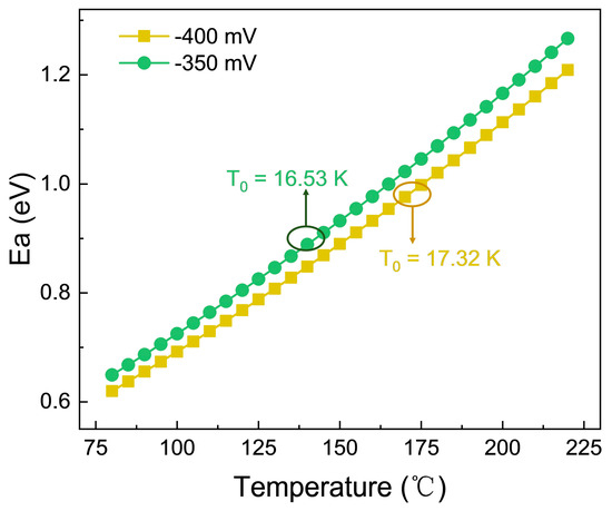
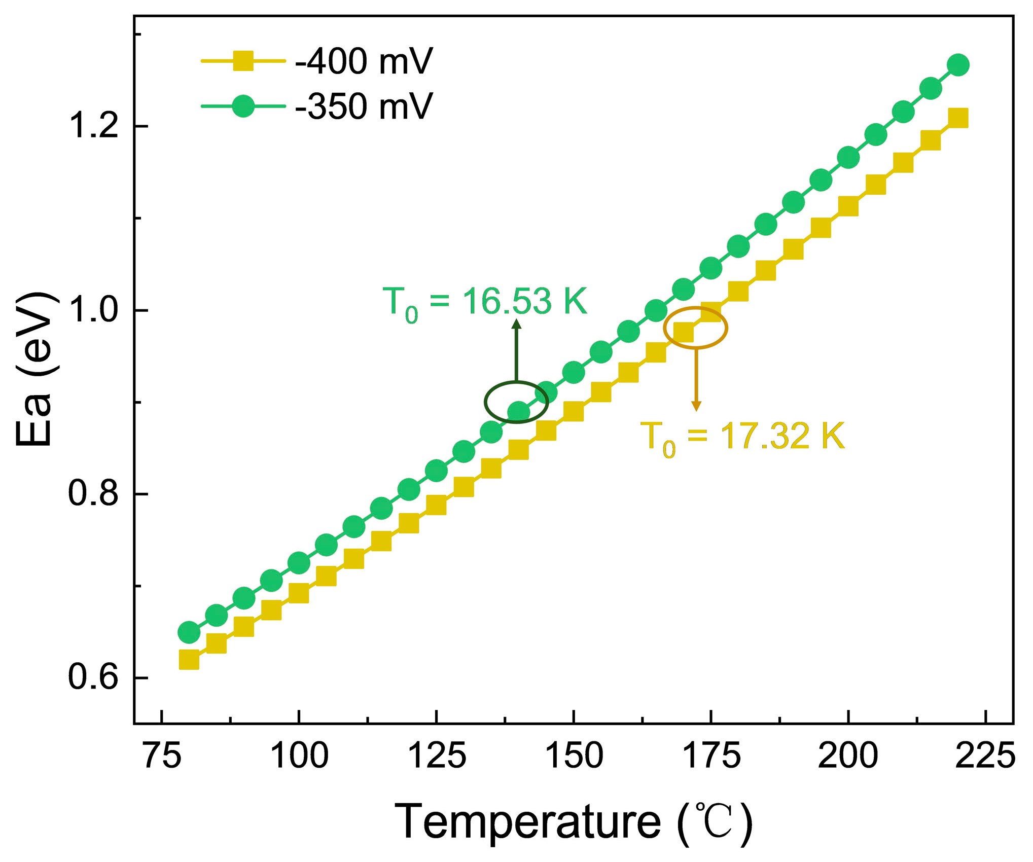
Subsequently, we calculated the activation energies (Ea) corresponding to different temperatures under two failure criteria, namely VSP = −400 mV and −350 mV, and presented the results in Figure 4. Comparative analysis reveals that the activation energies under both criteria increase with temperature, while the Ea values under the more stringent charge loss criterion (−350 mV) are systematically higher, which is attributed to its lower characteristic temperature T0. According to our calculations, the activation energies at 85 °C are 0.67 eV and 0.64 eV for the −400 mV and −350 mV criteria, respectively. This finding is consistent with the fundamental distinction between the T-model and the conventional Arrhenius model, as expressed in Equations (1) and (2): the Ea in the T-model varies with temperature, a characteristic that enhances its accuracy in data fitting.
Figure 4.
Curve of activation energy Ea versus temperature under the T-model.
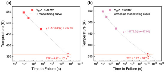
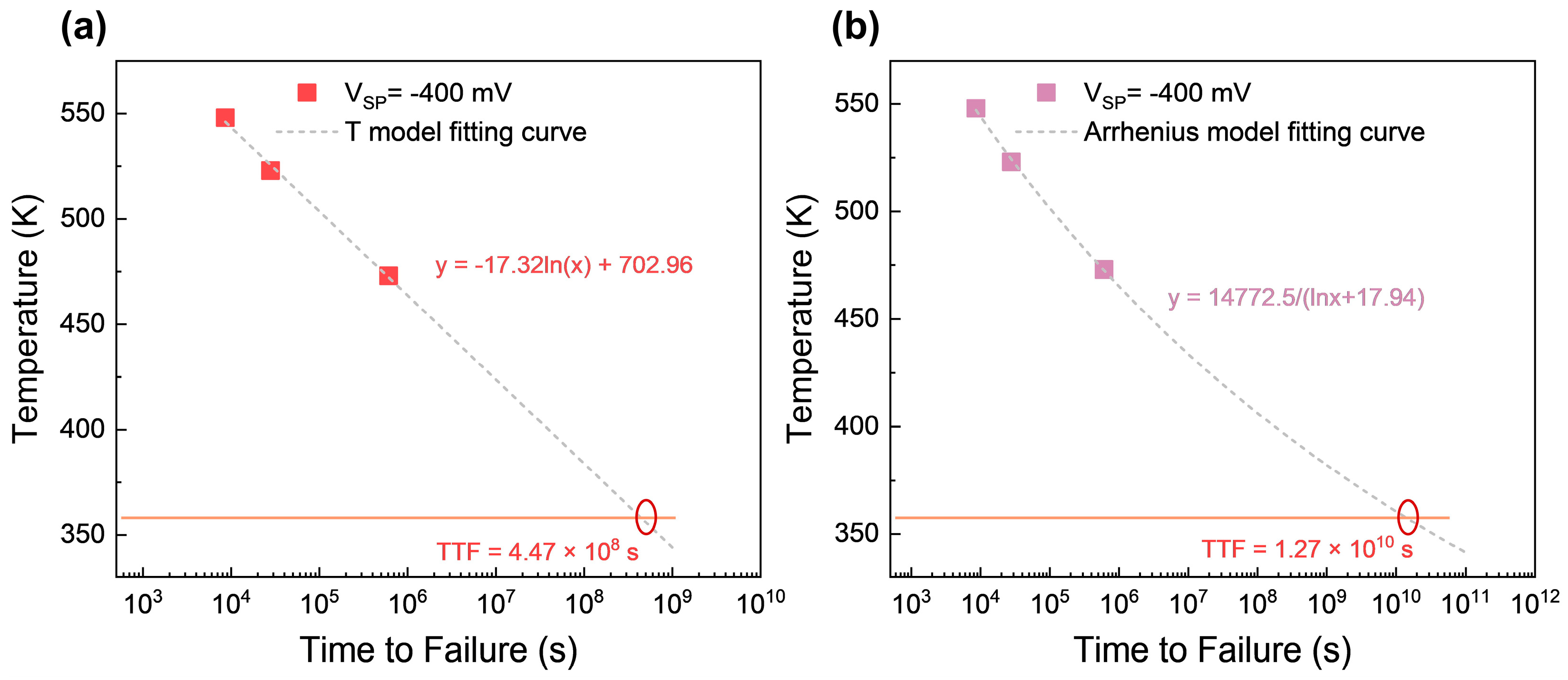
Figure 5 presents a comparative analysis between the T-model and the Arrhenius model under conditions where the failure VSP is −400 mV (charge loss = 47%). In this comparison, the T-model predicts a failure time of 4.47 × 10⁸ s (about 14.2 years) for the SONOS device under 85 °C baking conditions. Regarding charge transport mechanisms, charge leakage in FG devices primarily occurs through FN tunneling, wherein charge leaks from the floating gate conductor through the insulating layer. However, in SONOS devices, charge loss mechanisms involve multiple processes such as trap-assisted tunneling and thermal excitation. Consequently, the effective activation energy varies with temperature in such devices. This conservative estimate directly arises from the model’s incorporation of temperature-dependent activation energy—a key physical characteristic of SONOS charge loss mechanisms such as trap-assisted tunneling and thermal emission—which is not accounted for in the Arrhenius model. In contrast, the Arrhenius model, which assumes a constant activation energy across the entire temperature range, yields a more optimistic prediction of 1.27 × 10¹⁰ s (about 402.7 years). This discrepancy may stem from differences in the assumptions and methodologies employed by the two models in analyzing the relationship between charge leakage rate and temperature. The Arrhenius model typically assumes that charge leakage follows an exponential dependence on temperature, governed primarily by activation energy. The T-model, however, incorporates additional time-dependent factors, thereby offering a more conservative and cautious projection of long-term reliability.
Figure 5.
The relationship between baking temperature and failure time predicted by (a) T-model and (b) Arrhenius model. The red circle represents the predicted lifespan.
Based on the above discussion, the T-model was precisely fitted using experimental erased data from SONOS memories. The model demonstrates high accuracy in analyzing erasing operations, with strong agreement between predicted and measured data, validating its effectiveness and reliability. These results indicate that the T-model is well suited for predicting charge loss behavior during erase operations, providing a powerful tool for assessing the long-term stability of SONOS devices under such conditions. However, some discrepancies were observed between the programming data and the model predictions, which may be attributed to the complexity of charge injection mechanisms during programming and potential influencing factors such as programming voltage, temperature variations, and charge trapping phenomena. Due to these complexities, the T-model currently shows limitations in accurately predicting failure times for programming operations, suggesting a need for further refinement and investigation in future studies.
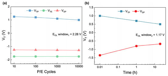
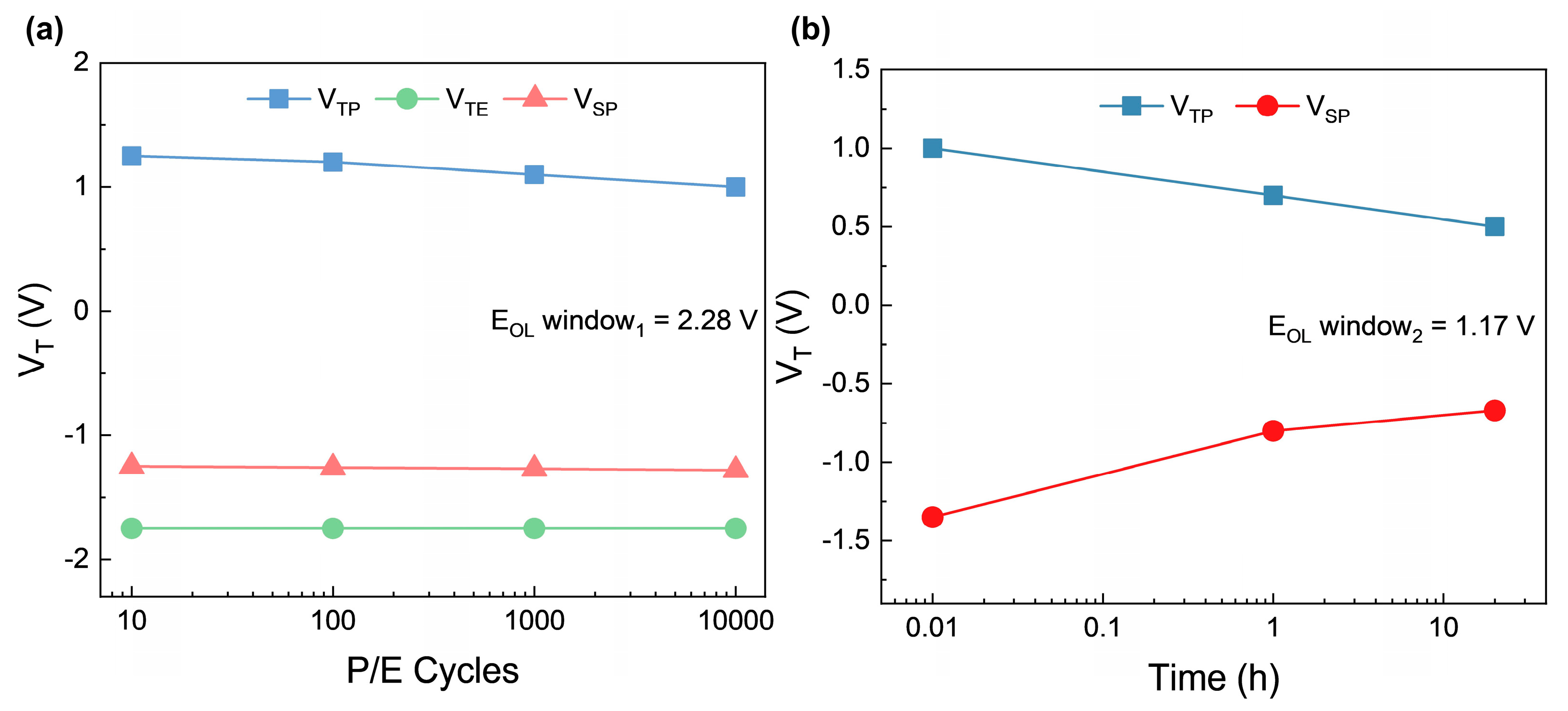
Subsequently, reliability performance of SONOS memory devices fabricated in the 28 nm HKMG process was evaluated. As shown in Figure 6a, high-temperature endurance tests were conducted on SONOS memory devices fabricated using a 28 nm HKMG process. The results demonstrate that even after 10,000 program/erase (P/E) cycles at 85 °C, the threshold voltage window exhibits only a slight degradation and remains 2.28 V, showing negligible deviation from the initial window. This outstanding performance is of significant engineering relevance, as high temperatures typically accelerate charge leakage and material degradation, while frequent P/E cycling can induce cumulative structural damage in memory cells. The ability to maintain such a wide memory window under these conditions highlights the device’s excellent charge trapping capability, high-quality tunneling oxide layer, and overall structural reliability. The robust endurance of the SONOS memory can be attributed to its specific structural characteristics. The relatively thin tunneling oxide layer minimizes the generation of excessive charge traps during repeated P/E operations, while the insulating charge trapping layer prevents catastrophic failure due to localized charge leakage, thereby preserving the functional integrity of the memory cell throughout the cycling tests.
Figure 6.
(a) Endurance test result for 28 nm HKMG SONOS memory at 85 °C; (b) data retention characteristics of 28 nm HKMG SONOS memory at 250 °C after endurance testing.
Afterwards, a systematic evaluation of the data retention characteristics of the SONOS memory device was conducted. Figure 6b specifically illustrates the retention performance after complete endurance testing. It is particularly noteworthy that even after undergoing high-temperature baking at 250 °C and a full endurance cycle test, the device’s threshold voltage window remains at an outstanding level of 1.17 V, far exceeding the minimum requirement of 0.4 V necessary for memory circuit design. Based on predictions from the T-model, the SONOS device is expected to achieve a data retention time exceeding 10 years at an operating temperature of 85 °C. These results not only confirm the outstanding charge retention capability of the device under extreme temperature conditions but also underscore its long-term reliability in harsh operating environments. The remarkable stability is attributed to an optimized gate dielectric stack and an innovative charge trapping mechanism, making it particularly suitable for applications demanding high temperature tolerance, such as automotive electronics and industrial control systems.
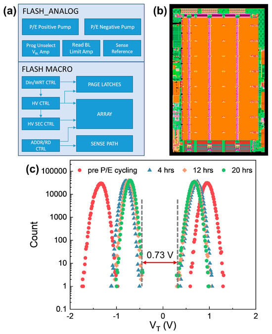
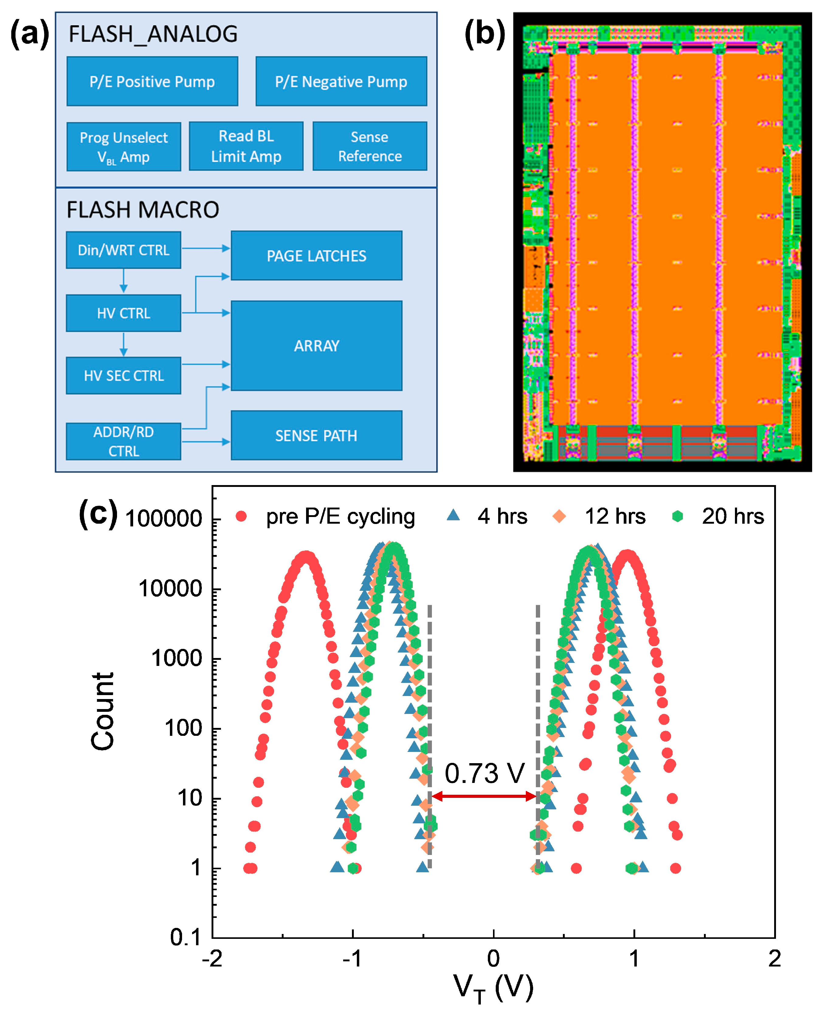
In addition to the reliability testing of individual SONOS memory cells, it is essential to evaluate the reliability of the memory array as a whole. The proper operation of a memory device relies on the coordinated functioning of multiple functional modules. As conceptually illustrated in Figure 7a, a complete SONOS memory chip consists of several key blocks, including the control module, voltage distribution module, clock module, and memory array. Figure 7b presents the layout of a 576 kB SONOS memory device fabricated in this study. The central region of the layout corresponds to the memory array. The array employs a 2T-type memory cell architecture, with each row containing 2048 bits. Furthermore, the memory supports parallel data input and output operations, with 32-bit simultaneous input and 128-bit simultaneous output capabilities.
Figure 7.
(a) Conceptual diagram of the SONOS memory functional module; (b) 576 kB SONOS memory layout; (c) P/E cycling test statistics for SONOS memory arrays under 250 °C at different bake time.
Figure 7c shows a comparison of the threshold voltage (VT) distributions for a SONOS memory array before and after program/erase (P/E) cycling, clearly demonstrating the device’s excellent endurance performance. The experimental data were obtained from four SONOS test wafers, with ten dies randomly selected per wafer. From each die, 1 million memory cells were characterized. The figure showed the median value of these 40 dies. This multi-wafer, multi-die sampling approach ensures statistical reliability and validates performance reproducibility both within individual wafers and across different fabrication batches. The test results indicate that after 100,000 program/erase (P/E) cycles at 85 °C, the memory cells maintain highly stable threshold voltage distributions with only minimal degradation, even under extended baking durations ranging from 4 to 20 h at 250 °C. It is particularly noteworthy that throughout the endurance tests, a constant-amplitude single-pulse programming and erasing scheme was employed, and the threshold voltage window consistently remained above 0.4 V. This outstanding behavior underscores the superior endurance characteristics of the SONOS memory array. The results further confirm that even under the most severe environmental conditions, the memory cells maintain high charge retention capability and P/E efficiency, offering a highly reliable solution for embedded memory applications.
4. Conclusions
In summary, this research presents a comprehensive framework for reliability assessment through the development of a novel temperature-dependent charge loss model (T-model) specifically designed for SONOS memory devices. The proposed T-model provides a more complete physical description of charge leakage dynamics compared to conventional approaches. Systematic validation was conducted using 2T-SONOS memory devices fabricated using 28 nm HKMG technology, with experimental data collected across multiple degradation levels and temperature conditions. The fitted model demonstrates exceptional predictive accuracy, particularly evident in its characteristic temperature parameter T0 = 19.07 K corresponding to a 33% charge loss at 85 °C which aligns closely with existing literature data. Furthermore, comparison with the conventional Arrhenius model reveals that under the failure criterion VSP = −400 mV, the T-model predicts a lifetime of approximately 14.2 years, whereas the Arrhenius model indicates 402.7 years. This demonstrates the T-model’s more conservative predictive characteristics, which stem from its incorporation of temperature-dependent activation energy—a key physical feature observed in SONOS charge loss that is not accounted for in the Arrhenius model. Beyond theoretical modeling, the experimental results confirm outstanding device reliability with the HKMG-integrated SONOS memory maintaining a threshold voltage window of 2.28 V after 10,000 program/erase cycles at 85 °C. Subsequently, following a 10 h bake at 250 °C, it still exhibited a threshold voltage window of 1.17 V. In addition, the SONOS memory array demonstrated exceptional endurance characteristics, maintaining highly stable threshold voltage distributions with minimal degradation after 10,000 P/E cycles while consistently preserving a threshold voltage window above 0.4 V throughout extended baking durations. Importantly, the chosen failure criterion (VSP = –400 mV, corresponding to 47% charge loss) is directly linked to the read window margin required for reliable circuit operation in embedded memory applications, thereby ensuring that the lifetime predictions are both physically meaningful and practically relevant for product qualification. These characteristics work synergistically to maintain a highly stable threshold voltage window throughout the device’s operational lifetime, providing critical performance guarantees for high-reliability storage applications under demanding conditions. The results confirm not only the feasibility of adopting HKMG technology in SONOS memory fabrication but also establish a comprehensive reliability evaluation benchmark. This work provides a scientific basis for long-term performance prediction and quality control, while offering practical guidance and a viable pathway for the development of high-density SONOS memory systems capable of long-term stable operation.
Author Contributions
X.Y.: Writing—original draft, Data curation, Conceptualization. B.C.: Writing—original draft, Data curation. S.W.: Formal analysis, Visualization. D.W.Z.: Writing—original draft, Conceptualization. All authors have read and agreed to the published version of the manuscript.
Funding
This research received no external funding.
Data Availability Statement
The original contributions presented in this study are included in the article. Further inquiries can be directed to the corresponding authors.
Conflicts of Interest
The authors declare that they have no known competing financial interests or personal relationships that could have appeared to influence the work reported in this paper.
References
- Liu, C.; Yang, Q.; Zeng, B.; Jiang, Y.; Zheng, S.; Liao, J.; Dai, S.; Zhong, X.; Zhou, Y.; Liao, M. Orientation Independent Growth of Uniform Ferroelectric Hf0.5Zr0.5O2 Thin Films on Silicon for High-Density 3D Memory Applications. Adv. Funct. Mater. 2022, 32, 2209604. [Google Scholar] [CrossRef] [Scilit]
- Chen, X.; Zhou, Y.; Roy, V.A.L.; Han, S. Evolutionary Metal Oxide Clusters for Novel Applications: Toward High-Density Data Storage in Nonvolatile Memories. Adv. Mater. 2017, 30, 1703950. [Google Scholar] [CrossRef] [Scilit]
- Aryana, K.; Gaskins, J.T.; Nag, J.; Stewart, D.A.; Bai, Z.; Mukhopadhyay, S.; Read, J.C.; Olson, D.H.; Hoglund, E.R.; Howe, J.M.; et al. Interface controlled thermal resistances of ultra-thin chalcogenide-based phase change memory devices. Nat. Commun. 2021, 12, 774. [Google Scholar] [CrossRef] [Scilit] [PubMed]
- Ma, J.; Liu, H.; Yang, N.; Zou, J.; Lin, S.; Zhang, Y.; Zhang, X.; Guo, J.; Wang, H. Circuit-Level Memory Technologies and Applications based on 2D Materials. Adv. Mater. 2022, 34, e2202371. [Google Scholar] [CrossRef] [Scilit] [PubMed]
- Kim, K.H.; Kim, N.; Kim, Y.K.; Kim, H.S.; Oh, H.B.; Kim, C.E.; Shin, H.W.; Kim, M.G.; Choi, W.J.; Jang, B.C. Material engineering to enhance reliability in 3D NAND flash memory. Device 2025, 3, 100682. [Google Scholar] [CrossRef] [Scilit]
- Chen, A. A review of emerging non-volatile memory (NVM) technologies and applications. Solid-State Electron. 2016, 125, 25–38. [Google Scholar] [CrossRef] [Scilit]
- Kim, K.; Choi, J. Future Outlook of NAND Flash Technology for 40nm Node and Beyond. In Proceedings of the 2006 21st IEEE Non-Volatile Semiconductor Memory Workshop, Monterey, CA, USA, 12–16 February 2006; pp. 9–11. [Google Scholar] [CrossRef] [Scilit]
- Kim, K. Technology for Sub-50nm DRAM and NAND Flash Manufacturing. In Proceedings of the IEEE InternationalElectron Devices Meeting, 2005. IEDM Technical Digest, Washington, DC, USA, 5 December 2005; pp. 323–326. [Google Scholar]
- Bi, J.S.; Xu, Y.N.; Xu, G.B.; Wang, H.B.; Chen, L.; Liu, M. Total Ionization Dose Effects on Charge-Trapping Memory with Al2O3/HfO2/Al2O3Trilayer Structure. IEEE Trans. Nucl. Sci. 2017, 65, 200–205. [Google Scholar] [CrossRef] [Scilit]
- Lue, H.-T.; Shih, Y.-H.; Hsieh, K.Y.; Liu, R.; Lu, C.-Y. Novel Soft Erase and Re-Fill Methods for a P/sup +/− Poly Gate Nitride Trapping Non-Volatile Memory Device with Excellent Endurance and Retention Properties. In Proceedings of the 2005 IEEE International Reliability Physics Symposium, 2005. Proceedings. 43rd Annual, San Jose, CA, USA, 17–21 April 2005; pp. 168–174. [Google Scholar] [CrossRef] [Scilit]
- Wang, S.-Y.; Lue, H.-T.; Du, P.-Y.; Liao, C.-W.; Lai, E.-K.; Lai, S.-C.; Yang, L.-W.; Yang, T.; Chen, K.-C.; Gong, J.; et al. Reliability and Processing Effects of Bandgap-Engineered SONOS (BE-SONOS) Flash Memory and Study of the Gate-Stack Scaling Capability. IEEE Trans. Device Mater. Reliab. 2008, 8, 416–425. [Google Scholar] [CrossRef] [Scilit]
- Iizuka, H.; Masuoka, F.; Sato, T.; Ishikawa, M. Electrically alterable avalanche-injection-type MOS READ-ONLY memory with stacked-gate structure. IEEE Trans. Electron Devices 1976, 23, 379–387. [Google Scholar] [CrossRef] [Scilit]
- Shih, Y.; Lai, E.; Hsieh, J.; Hsu, T.; Wu, M.; Ni, K.; Chou, T.; Yang, L.; Hsieh, K.; Liaw, M.; et al. Highly Scalable and Reliable Multi-bit/cell Nitride Trapping Nonvolatile Memory Using Enhanced ANS-ONO Process with A Nitridized Interface. In Proceedings of the 2006 International Electron Devices Meeting, Washington, DC, USA, 11–13 December 2006; pp. 1–4. [Google Scholar] [CrossRef] [Scilit]
- Arreghini, A.; Akil, N.; Driussi, F.; Esseni, D.; Selmi, L.; van Duuren, M. Characterization and modeling of long term retention in SONOS non volatile memories. In Proceedings of the ESSDERC 2007—37th European Solid State Device Research Conference, Munich, Germany, 11–13 September 2007; pp. 406–409. [Google Scholar] [CrossRef] [Scilit]
- Park, Y.; Choi, J.; Kang, C.; Lee, C.; Shin, Y.; Choi, B.; Kim, J.; Jeon, S.; Sel, J.; Park, J.; et al. Highly Manufacturable 32Gb Multi-Level NAND Flash Memory with 0.0098 μm2 Cell Size using TANOS(Si-Oxide-Al2O3-TaN) Cell Technology. In Proceedings of the 2006 International Electron Devices Meeting, Washington, DC, USA, 11–13 December 2006; pp. 1–4. [Google Scholar] [CrossRef] [Scilit]
- Kim, S.S.; Yong, S.K.; Kim, W.; Kang, S.; Park, H.W.; Yoon, K.J.; Sheen, D.S.; Lee, S.; Hwang, C.S. Review of Semiconductor Flash Memory Devices for Material and Process Issues. Adv. Mater. 2022, 35, e2200659. [Google Scholar] [CrossRef] [Scilit]
- Ramkumar, K. Materials and Device Reliability in SONOS Memories. In Charge-Trapping Non-Volatile Memories: Volume 2—Emerging Materials and Structures; Dimitrakis, P., Ed.; Springer International Publishing: Cham, Switzerland, 2017; pp. 1–54. [Google Scholar]
- Guo, X.; Yue, S.; Li, J.; Zhou, T.; Zha, Q. Total ionizing dose effects on data retention characteristics of 55nm SONOS flash. J. Phys. Conf. Ser. 2021, 1983, 012061. [Google Scholar] [CrossRef] [Scilit]
- Chen, T.-S.; Wu, K.-H.; Chung, H.; Kao, C.-H. Performance Improvement of SONOS Memory by Bandgap Engineering of Charge-Trapping Layer. IEEE Electron Device Lett. 2004, 25, 205–207. [Google Scholar] [CrossRef]
- Meena, J.S.; Sze, S.M.; Chand, U.; Tseng, T.-Y. Overview of emerging nonvolatile memory technologies. Nanoscale Res. Lett. 2014, 9, 526. [Google Scholar] [CrossRef] [Scilit]
- Steimle, R.; Muralidhar, R.; Rao, R.; Sadd, M.; Swift, C.; Yater, J.; Hradsky, B.; Straub, S.; Gasquet, H.; Vishnubhotla, L.; et al. Silicon nanocrystal non-volatile memory for embedded memory scaling. Microelectron. Reliab. 2007, 47, 585–592. [Google Scholar] [CrossRef] [Scilit]
- Hsu, H.-H.; Lee, J.Y.-M. Electrical characterization of metal-oxide-high-k dielectric-oxide-semiconductor (MOHOS) structures for memory applications. Microelectron. Reliab. 2007, 47, 606–609. [Google Scholar] [CrossRef] [Scilit]
- Arreghini, A.; Akil, N.; Driussi, F.; Esseni, D.; Selmi, L.; van Duuren, M. Long term charge retention dynamics of SONOS cells. Solid State Electron. 2008, 52, 1460–1466. [Google Scholar] [CrossRef] [Scilit]
- Bu, J.; White, M. Effects of two-step high temperature deuterium anneals on SONOS nonvolatile memory devices. IEEE Electron Device Lett. 2001, 22, 17–19. [Google Scholar] [CrossRef] [Scilit]
- Nozawa, H.; Kohyama, S. A Thermionic Electron Emission Model for Charge Retention in SAMOS Structure. Jpn. J. Appl. Phys. 1982, 21, L111–L112. [Google Scholar] [CrossRef] [Scilit]
- Menzinger, M.; Wolfgang, R. The Meaning and Use of the Arrhenius Activation Energy. Angew. Chem. Int. Ed. Engl. 1969, 8, 438–444. [Google Scholar] [CrossRef] [Scilit]
- Herrmann, M.; Schenk, A. Field and high-temperature dependence of the long term charge loss in erasable programmable read only memories: Measurements and modeling. J. Appl. Phys. 1995, 77, 4522–4540. [Google Scholar] [CrossRef] [Scilit]
- Pan, C.-S.; Wu, K.; Chin, D.; Sery, G.; Kiely, J. High-temperature charge loss mechanism in a floating-gate EPROM with an oxide-nitride-oxide (ONO) interpoly stacked dielectric. IEEE Electron Device Lett. 1991, 12, 506–509. [Google Scholar] [CrossRef] [Scilit]
- De Salvo, B.; Ghibaudo, G.; Pananakakis, G.; Guillaumot, B.; Candelier, P.; Reimbold, G. A new extrapolation law for data-retention time-to-failure of nonvolatile memories. IEEE Electron Device Lett. 1999, 20, 197–199. [Google Scholar] [CrossRef] [Scilit]
- De Salvo, B.; Ghibaudo, G.; Pananakakis, G.; Reimbold, G.; Mondond, F.; Guillaumot, B.; Candelier, P. Experimental and theoretical investigation of nonvolatile memory data-retention. IEEE Trans. Electron Devices 1999, 46, 1518–1524. [Google Scholar] [CrossRef] [Scilit]
- White, M.; Adams, D.; Murray, J.; Wrazien, S.; Zhao, Y.; Wang, Y.; Khan, B.; Miller, W.; Mehrotra, R. Characterization of scaled SONOS EEPROM memory devices for space and military systems. In Proceedings of the 2004 Non-Volatile Memory Technology Symposium, Orlando, FL, USA, 15–17 November 2004; pp. 51–59. [Google Scholar]
- Ramkumar, K.; Prabhakar, V.; Keshavarzi, A.; Kouznetsov, I.; Geha, S. SONOS Memories: Advances in Materials and Devices. MRS Adv. 2017, 2, 209–221. [Google Scholar] [CrossRef] [Scilit]
- Novikov, Y.N.; Gritsenko, V.A. Discrete trapping levels of localized states in amorphous silicon nitride. J. Appl. Phys. 2024, 136, 014101. [Google Scholar] [CrossRef] [Scilit]
- Hsiao, Y.-H.; Lue, H.-T.; Lee, M.Y.; Huang, S.-C.; Chou, T.-Y.; Wang, S.-Y.; Hsieh, K.-Y.; Liu, R.; Lu, C.-Y. A study of SONOS charge loss mechanism after hot-hole stressing using trap-layer engineering and electrical re-fill methods. In Proceedings of the 2008 IEEE International Reliability Physics Symposium (IRPS), Phoenix, AZ, USA, 27 April–1 May 2008; pp. 695–696. [Google Scholar] [CrossRef] [Scilit]
- Lue, H.-T.; Hsiao, Y.-H.; Shih, Y.-H.; Lai, E.-K.; Hsieh, K.-Y.; Liu, R.; Lu, C.-Y. Study of Charge Loss Mechanism of SONOS-Type Devices using Hot-Hole Erase and Methods to Improve the Charge Retention. In Proceedings of the 2006 IEEE International Reliability Physics Symposium Proceedings, San Jose, CA, USA, 26–30 March 2006; pp. 523–529. [Google Scholar] [CrossRef] [Scilit]
- Roizin, Y.; Yankelevich, A.; Netzer, Y. Novel Techniques for Data Retention and Leff Measurements in Two Bit microFLASH® Memory Cells. In Proceedings of the 2000 International Conference on Characterization and Metrology for ULSI Technology, Gaithersburg, MA, USA, 26–29 June 2000; Volume 550, pp. 181–185. [Google Scholar] [CrossRef] [Scilit]

Disclaimer/Publisher’s Note: The statements, opinions and data contained in all publications are solely those of the individual author(s) and contributor(s) and not of MDPI and/or the editor(s). MDPI and/or the editor(s) disclaim responsibility for any injury to people or property resulting from any ideas, methods, instructions or products referred to in the content. |
© 2026 by the authors. Licensee MDPI, Basel, Switzerland. This article is an open access article distributed under the terms and conditions of the Creative Commons Attribution (CC BY) license.