


Abstract
As the process node is scaled down, the spin-transfer-torque magnetic random-access memory (STT-MRAM) exhibits higher memory density than the static random-access memory (SRAM), making it one of the more promising successors of the low-level on-chip cache memory. However, the low read margin (RM) of the magnetic tunnel junction (MTJ) in STT-MRAM can limit the achievable read accuracy. We implemented 2-bit channel quantization for error-correcting code (ECC) schemes and explored the trade-offs between improved read accuracy and factors such as circuit area, power consumption, and latency. The proposed quantization scheme consists of a sensing amplifier-based 2-bit quantizer and MTJ resistor-based soft-decision thresholds. Compared to 1-bit channel quantization using the Bose–Chaudhuri–Hocquenghem (BCH) code, the proposed 2-bit quantization architecture achieves a fourfold reduction in frame error rate (FER) from to when paired with polar codes and successive cancellation (SC) decoding. Additionally, this approach results in decoding complexity that is only 1/13th of that required for BCH at a 0.7 code rate.
1. Introduction
As complementary metal–oxide–semiconductor (CMOS) technology scales into the few-nanometer regime, the conventional six-transistor (6T) static random-access memory (SRAM) cell is widely regarded as increasingly area-limited for high-density on-chip cache, largely because the bitcell footprint does not scale as efficiently as logic with advanced design-rule constraints [1]. Meanwhile, spin-transfer-torque magnetic random-access memory (STT-MRAM) has been extensively studied as an embedded memory option that can provide competitive density and near-zero standby leakage compared with SRAM, making it attractive for energy-constrained cache-like applications [2,3]. Leading semiconductor companies have already demonstrated embedded STT-MRAM on 40/28/22 CMOS nodes [4], further validating its potential for commercial adoption.
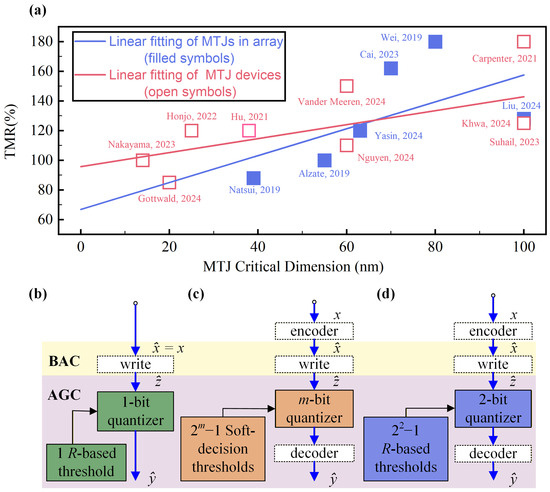
Within the cell, STT-MRAM uses a magnetic tunnel junction (MTJ) resistor to store one-bit binary data. The MTJ can be in a parallel state with a resistance of or in an antiparallel state with . The tunneling magnetoresistance (TMR) of the MTJ represents the relative difference between its high- and low-resistance states and is defined as , where the average resistance in the high-resistance state is = and in the low-resistance state is = [5]. Despite increased density, the reading accuracy of STT-MRAM decreases as the MTJ size is reduced with smaller process nodes, leading to a reduction in TMR, as shown in Figure 1a [6,7,8,9,10,11,12,13,14,15,16,17,18,19,20].
Figure 1.
(a) The TMR reduces as the diameter of the MTJ decreases for both discrete MTJ devices and the MTJ in a large array, adapted from [6,7,8,9,10,11,12,13,14,15,16,17,18,19,20]. (b) The conventional SA-based 1-bit channel quantization. (c) Multi-bit channel quantization using soft-decision thresholds. (d) The proposed 2-bit channel quantization circuits using MTJ resistor-based thresholds.
STT-MRAM can be described by a combined binary asymmetric channel and asymmetric Gaussian channel (BAC-AGC) model, as shown in Figure 1b–d [21]. The variations caused by process, voltage, temperature (PVT), and other environmental noise affect the distribution of MTJ resistance. The asymmetric Gaussian channel (AGC) can describe the resistance states of MTJ as both follow a Gaussian distribution, as shown in Figure 2d [21,22]. Let and denote the standard deviations of the two resistance states. As the MTJ scales down, both and increase, with reported deviations ranging from 5 to 27% [10,23,24].
Figure 2.
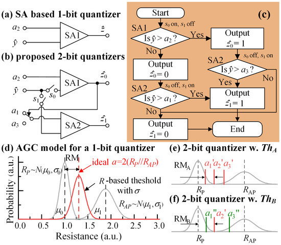
The diagrams of the (a) conventional SA-based 1-bit quantizer and (b) proposed SA-based 2-bit quantizers. (c) The flow chart of 2-bit channel quantization. The RM of the AGC model changes when using (d) 1-bit or (e,f) 2-bit channel quantization. AGC: Asymmetric Gaussian channel.
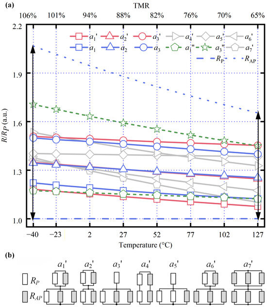
To read the MTJ data cells, a sense amplifier (SA) functions as a 1-bit quantizer, executing 1-bit channel quantization in conjunction with the hard decision threshold , which is provided by the MTJ reference cell, as shown in Figure 2a. The reading margin (RM) of STT-MRAM is calculated as [25]. As TMR decreases, RM will also decrease. Figure 3a shows that the temperature-dependent TMR reduces by 39%. An RM of 6 is reported to be required for a 32 Mb memory array to obtain a read yield of 96.74% [25]. A low RM (<3) not only elevates the bit error rate (BER) to 0.27% but also threatens cache coherence in multi-core systems. For instance, frequent read errors may propagate corrupted data to lower cache hierarchies, triggering silent data corruption or even system-level failures due to inconsistent cache states [26]. Additionally, because the MTJs in the reference cells are the same as those in the data cells, also experiences fluctuations in variance . As shown in Figure 2d, this variance further reduces the RM. It indicates that when the process node scales down, STT-MRAM achieves increased array density but suffers from a decline in read accuracy.
Figure 3.
(a) Normalized low-resistance value of the MTJ devices with = 88% @ 27 °C, . The normalized ideal thresholds and the seven candidate thresholds (∼) as functions of the TMR as well as the temperature. The normalized , are also plotted. for quantizer A; for quantizer B. (b) The candidate thresholds ∼ are determined by the MTJ resistor networks with either or .
Recent embedded STT-MRAM demonstrations for SRAM-like working-memory applications show that retention can be intentionally relaxed to trade for faster writing and higher endurance, while system-level mitigation is used to bound the resulting time-accumulated errors [27]. Specifically, a built-in read–modify–write scrubbing controller periodically reads the array, checks latent errors with an on-chip error-correcting code (ECC), and rewrites corrected data such that the accumulated errors stay within the ECC correction capability [27]. Under accelerated stress and conservative extrapolation models, the measured write endurance can exceed cycles, substantially higher than NVM-oriented STT-MRAM targets [27]. These results further motivate improving read reliability under a reduced sensing margin, as a lower raw read error rate directly reduces ECC burden and the frequency and overhead of corrective actions such as scrubbing.
This presents an opportunity to implement multi-bit channel quantization and comprehensive ECC schemes to enhance the overall read accuracy of STT-MRAM [21,22], such as fixed-code ECC [6,22,28,29] and adaptive ECC schemes [30,31]. The low-level cache applications require dual- or triple-error correction (TEC) ECC instead of the single-error correction (SEC) code for the commercial standalone STT-MRAM [6,30]. When using SA as a 1-bit quantizer, it was found that the Bose–Chaudhuri–Hocquenghem (BCH) code can significantly enhance read accuracy [29,31].
For the MTJ channel, using non-uniform multi-bit quantization can significantly improve the signal-to-noise ratio (SNR) [21]. In combination with low-density parity-check (LDPC) and polar codes, multi-bit quantization can reduce the read error rate by 1∼2 orders of magnitude compared to the SEC schemes when RM is low, as shown in Figure 1c [22,28,29]. However, algorithms like dynamic programming are still needed to find the best soft-decision thresholds [32], and multi-bit channel quantization has not been implemented in circuitry.
In this paper, we implemented 2-bit channel quantization circuits for ECC to enhance the read accuracy of STT-MRAM with low-RM MTJ by integrating an SA-based 2-bit quantizer with the MTJ resistor-based (R-based) soft-decision thresholds, as shown in Figure 1d. We compared the proposed 2-bit quantizers in terms of area, power consumption, latency, and overall read accuracy. We introduce a self-generated and adaptive threshold implementation based on an MTJ–resistor network. In this approach, non-uniform soft-decision thresholds are synthesized directly from compact combinations of and , eliminating the need for look-up table (LUT)-programmed threshold sets or auxiliary digital-to-analog converters (DACs). The matched resistor–MTJ structure inherently tracks resistance variations under PVT and device drift, removing the requirement for explicit PVT sensing and control logic. Additionally, a full-margin SA is employed to enhance the second-bit decision margin under low read-margin conditions. Moreover, we investigated the performance of various ECC schemes using the proposed non-uniform 2-bit quantization for the STT-MRAM with low RM. This paper is organized as follows. Section 2 introduces a modified cascaded BAC–AGC channel model that accounts for PVT-induced variations. Section 3 details the circuit implementation of the proposed 2-bit channel quantization, including the MTJ–resistor soft-decision thresholds and quantizer architectures. Section 4 assesses the ECC performance under different code rates and decoding algorithms with the proposed 2-bit quantization. Section 5 concludes the paper.
2. Modified Cascaded BAC–AGC Channel Model for STT-MRAM Under PVT-Induced Variations
In the STT-MRAM, the PVT-induced fluctuations broaden the resistance distribution and reduce the TMR of the MTJs, which prevents the sensing circuitry from achieving sufficient read yield. The overall error increase arises from the write errors, the read disturb errors, and the read decision errors [21]. Since the in-cell MTJ switching events are asymmetric and independent of each other [33], the transfer functions of the STT-MRAM induced by the write error can be described by a binary asymmetric channel (BAC). Successively, the single direction miswriting leads to the read disturb error, which is similar to the write error and can be described by the BAC. Moreover, as the reading and writing circuits share the same paths in the memory array, the read disturb error rate of can be described by the Z channel model which can be combined into the BAC model [21]. When the reading current is set to the write-0 () direction, the crossover probability of the BAC can be written as [33]
where ,, and , , are the error rate, the correct rate, and the write error rate for transmitting and , respectively. When assuming a switching probability of 50%, the crossover probabilities of BAC are for and for .
Let x denote the input of the BAC, which is always . The output y is quantized as outputs by a q-bit quantizer. Let denote the boundaries of the quantization interval, where , . denotes the j-th quantization interval, [21].
In the BAC, we can define the averaged resistances of the low-resistance state () and the high-resistance state () of the MTJ as and , respectively. As the resistance distributions of both states follow the Gaussian distribution [21], we use and to denote the variations in two resistance states which are caused by process-induced tunneling oxide thickness () fluctuations of the MTJ. When the pitch size of the MTJ reduces, the resistance distribution broadens, which makes the and increase simultaneously [21,25]. In this case, the assumption of is feasible as well [21].
In the STT-MRAM, the SAs are used as the 1-bit quantizer and the decision threshold is given by the reference cell resistances, dividing the reading margin into two intervals. The read decision errors induced by the sensing circuitry can be modeled as an asymmetric Gaussian channel (AGC), the transfer probability of which can be cascaded after BAC, which yields [21]
with , where is the right tail probability of the normal distribution. As the read decision error depends on the read accuracy of the SA, the variances in the read errors of different SA solutions can differ as much as 2.4 times [25]. Therefore, based on (1) and (2), the transfer probabilities of the cascade BAC-AGC channel can be modified as
where are the channel transfer probabilities of the modified BAC-AGC channel and the read accuracy of the quantizer. and , represent the error rate for the transmission from 0 to 1 and from 1 to 0 and the correct rate for the transmission from 0 to 0 and from 1 to 1.
3. Circuit Implementation of 2-Bit Channel Quantization Using MTJ–Resistor Soft Thresholds
The proposed 2-bit quantization implementation consists of R-based soft-decision thresholds and a 2-bit quantizer, as shown in Figure 1d.
3.1. MTJ–Resistor Network for Self-Adaptive Soft-Decision Threshold Generation
STT-MRAM requires non-uniform multi-bit quantization and adaptive thresholds to account for PVT variations. In channel quantization, the RM can be improved by using the optimal soft-decision thresholds. Current multi-bit quantization uses search algorithms to identify the optimal set that meets criteria such as maximizing the cutoff rate (MCR) [21]. Although the optimal thresholds can be implemented using a predetermined lookup table, they may require PVT sensing modules, additional control logic, and sets of reference cells. We propose using selected MTJ resistor networks to directly establish the soft-decision thresholds. The R-based thresholds are inherently non-uniformly quantized and self-adaptive to PVT changes, which enhances the compactness and power efficiency of the threshold generation circuits.
The seven possible resistor networks for the proposed 2-bit quantizer are , and . Figure 3b shows the layouts of the candidate resistor networks. To determine whether these candidate thresholds can sit close to the optimal ones in the low-TMR cases, we calculate their MCR in the BAC-AGC [21,22]. Then, the best candidate threshold sets can be determined when their is closest to the predetermined MCR as provided by the dynamic programming algorithm [21]. Embedded STT-MRAM is designed for over 10-year retention and -cycle endurance [34]; under such specifications, long-term drift of and is negligible.
In particular, for a 2-bit quantization channel with binary input, a set of soft-decision thresholds is required. Assuming the write error rates and , °C when the MTJ diameter is <40 [13], and for the 28 process [23]. We first determined of the optimal thresholds while keeping the initial conditions fixed. Secondly, for each candidate threshold (∼), their overall difference to over the points in the range of ∼ can be written as . Once the ith candidate threshold has the minimum to , we can use the to replace the latter. Therefore, we can use the threshold set with , , and to replace . As shown in Figure 3a, these R-based thresholds can self-adjust to match the optimal thresholds when RM decreases.
3.2. Read-Margin Expansion via Full-Margin Sense Amplifier for the Second-Bit Decision
Figure 2e shows the 2-bit channel quantization for BAC-AGC using , which can be used by 2-bit quantizer A or an analog-to-digital converter (ADC) circuit. For 2-bit quantizer A, when the first digit is “0”, the RM for the second digit quantization becomes . For , , which is lower than 3, the lower limit for ECC decoding. To broaden the RM for the second digit quantization, we propose using the full-margin SA as the quantizer [35], denoted as 2-bit quantizer B. As shown in Figure 2f, the thresholds for quantizer B are . In this case, the thresholds of quantizer B become and instead of and . This expands the RM for the second digit quantization, which becomes when the first digit is “0” and . As shown in Figure 3a, we note that for , which is almost 0.65 times that of .
3.3. Quantizer Architecture Comparison with R-Based Thresholds
For 2-bit channel quantization, both the SA and the ADC are candidates for implementing the quantizer circuit. The SA-based 2-bit quantizer was constructed using SA1 to quantize the first digit and SA2 to quantize the second digit, as shown in Figure 2b. Figure 2c shows the quantization process. Both SA-based 2-bit quantizers use a precharge sense amplifier (PCSA) as the SA1. The 2-bit quantizer A uses a PCSA as the SA2. The 2-bit quantizer B uses an improved multi-bit current-sensitive amplifier (IMB-CSA) as the SA2 [35]. Unlike traditional PCSAs, the IMB-CSA enhances the sensing margin through two mechanisms: (1) A symmetric current-path design eliminates charge-sharing effects during evaluation, directly boosting signal differential by 43%. (2) Negative-feedback adaptive bias compensation dynamically suppresses PVT-induced offsets, decoupling thresholds from MTJ parameter drift. This combined approach improves the read margin while maintaining accuracy under reduced TMR.
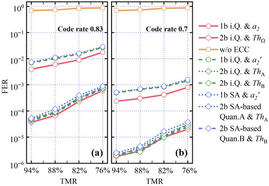
The gain in overall read accuracy involves trade-offs with the increasing circuit area, power consumption, and latency, inspired by multi-objective optimization frameworks in STT-MRAM design [22,28]. We define for evaluation, where P, T, and A represent power consumption, read latency, and the area, respectively. FER is defined as the single-pass post-ECC frame error rate under worst-case read conditions, used to compare quantization and ECC trade-offs. Prior FER-based studies on emerging memories use the low-FER regime () for design comparison, with ∼ as typical operating points [36,37]. Hence, the reported FER values are intended for comparative evaluation under worst-case sensing conditions, not as overall reliability targets. A larger indicates a better overall trade-off among power, latency, area, and FER. Figure 4a,b show that the ideal 1-bit quantizer using the polar code with successive cancellation (SC) decoding can reduce FERs by ∼ times. For the polar code using ideal 2-bit quantizers and SC decoding, the FER gains two orders of magnitude further reduction. When using R-based thresholds and , the FER increases slightly compared to . When the quantizer takes into account the error of the actual SA, the FER will further increase. Compared to 2-bit quantizer A, 2-bit quantizer B can achieve a ≈30% lower FER due to its higher RM when the code rate is 0.7, .
Figure 4.
The FERs of the polar code with SC decoding as functions of the temperature are shown when using the 2-bit and 1-bit ideal quantizers. The code rates are 0.83 for (a) and 0.7 for (b). When considering SA-induced read errors, the FERs for those ECC schemes are also plotted. For comparison, the cases without the ECC scheme are also shown. i.Q.: ideal quantizer.
To determine the , we simulated the P, T, and A of the proposed 2-bit quantizer circuits using the SMIC 28 CMOS process, as shown in Table 1. The of the proposed 2-bit quantization schemes was at least four times larger than that of the 1-bit case. The areas of both SA-based 2-bit quantizer circuits are smaller than that of a 2-bit flash ADC. However, only 2-bit quantizer A can achieve lower latency than the ADC scheme. Furthermore, the ADC scheme demonstrates the lowest power consumption. We note that the of 2-bit quantizer A is three times larger than that of the 2-bit ADC scheme, owing to its compact area and low latency. The 2-bit quantizer B can achieve the lowest FER, but this comes at the expense of increased area, power consumption, and latency. The energy efficiency improvement claimed in this work arises from the proposed resistance-based threshold generation method, rather than from Quantizer B alone. Quantizer B is designed to achieve extremely low FERs under low read-margin conditions, thereby reducing the need for re-reads or retries and lowering the average energy per successful read in reliability-critical scenarios. Quantizer A, meanwhile, is optimized for low-power operation. The efficiency benefit of the proposed threshold implementation applies to both quantizers.
Table 1.
Comparison of different quantizer circuits (.
4. ECC Performance with the Proposed 2-Bit Quantization
Using the proposed 2-bit channel quantization schemes, we compared the error correction performance of various ECC encoding and decoding schemes, including LDPC with reliability-based iterative min-sum (RBI-MS) decoding, the polar code with SC decoding, and the polar code with the cyclic redundancy check-successive cancellation list (CRC-SCL) algorithm. For comparison, the encoded input binary signal should pass through the same BAC-AGC. The choice of code rates and is motivated by their relevance as typical high-rate ECC regimes in embedded memory and cache contexts. Firstly, the design of cache/memory ECC involves a fundamental trade-off between reliability enhancement and redundancy-induced overhead. Consequently, high-rate codes are frequently employed as a redundancy-constrained reference in comparative evaluations [38,39]. Secondly, embedded memory ECC is commonly implemented at a predetermined access granularity, typically ranging from tens to several hundred bits, which necessitates the use of short-block code structures [40]. In line with these considerations, Table 2 presents short-block code configurations corresponding to the two selected rates, facilitating a fair and meaningful comparison. The word lengths and information bit numbers of the chosen ECC schemes at different code rates are shown in Table 2.
Table 2.
The for ECC schemes with different decoders †.
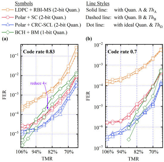
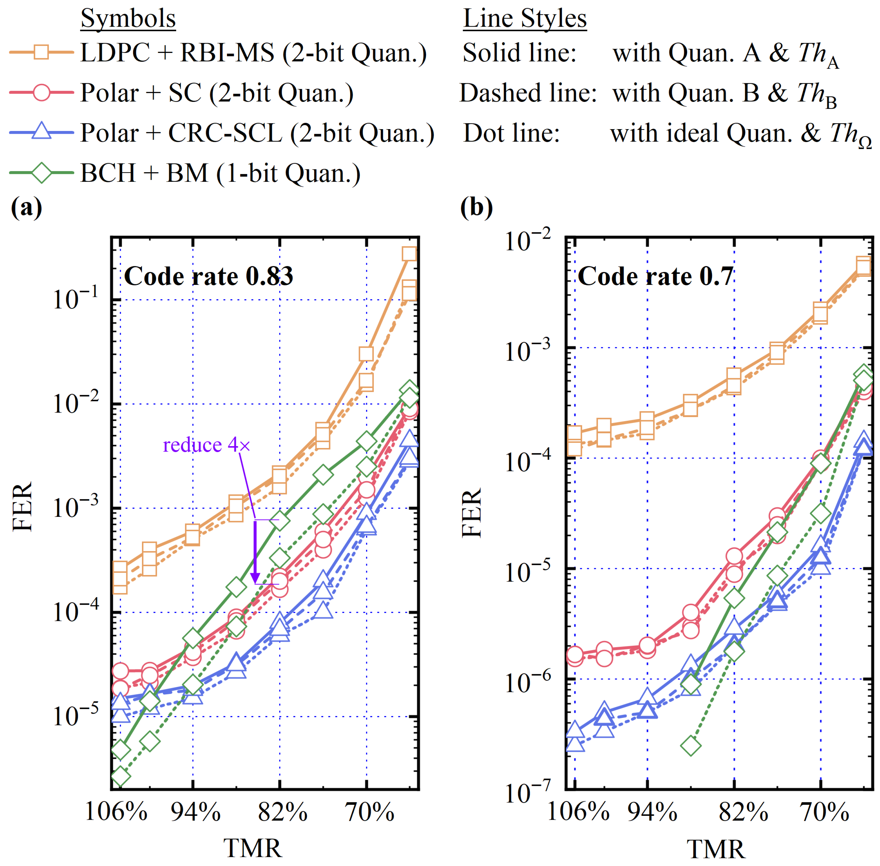
Figure 5a compares the FERs of three different ECC schemes at a code rate of 0.83 when using the proposed 2-bit quantizers. To provide a fair comparison, we included the FER of the BCH scheme using a 1-bit quantizer, with thresholds of and , and the Berlekamp–Massey (BM) decoding algorithm. As shown in Figure 5a, the BCH scheme with 1-bit quantization achieves the lowest FER among the ECC schemes when the RM is high . However, its FER increases rapidly as the RM decreases. In such cases, the polar code schemes using SC decoding or the CRC-SCL algorithm perform better than the BCH schemes. As shown in Figure 5b, when the code rate is 0.7, under low RM , the polar code with CRC-SCL can achieve the lowest FER among all the schemes. In Table 2, the different s of are 1.9 and 4 times lower than those of at code rates of 0.83 and 0.7, respectively. As the FER of is closer to that of , the of 2-bit quantizer B shown in Table 1 reduces less than the other non-ideal thresholds. As shown in Figure 5a, in the low-RM case with a code rate of 0.83, the polar code scheme using the SC decoder, 2-bit quantizer A, and can achieve an FER that is four times lower than that of the BCH schemes.
Figure 5.
The output FER of the LDPC code with RBI-MS and the polar code with SC or CRC-SCL decoding as functions of TMR when using different 2-bit quantizers are presented for code rates of (a) 0.83 and (b) 0.7, respectively. Here, and . For comparison, the FERs of BCH code schemes when using the ideal 1-bit quantizer are also shown.
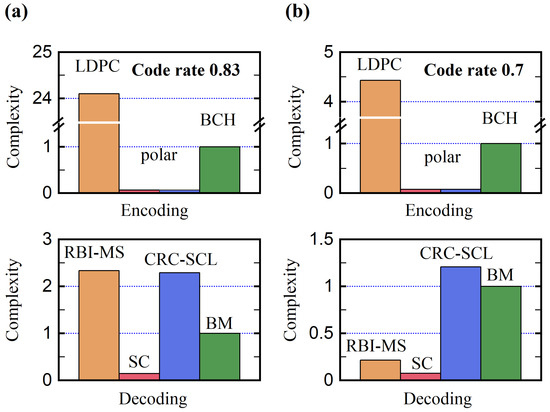
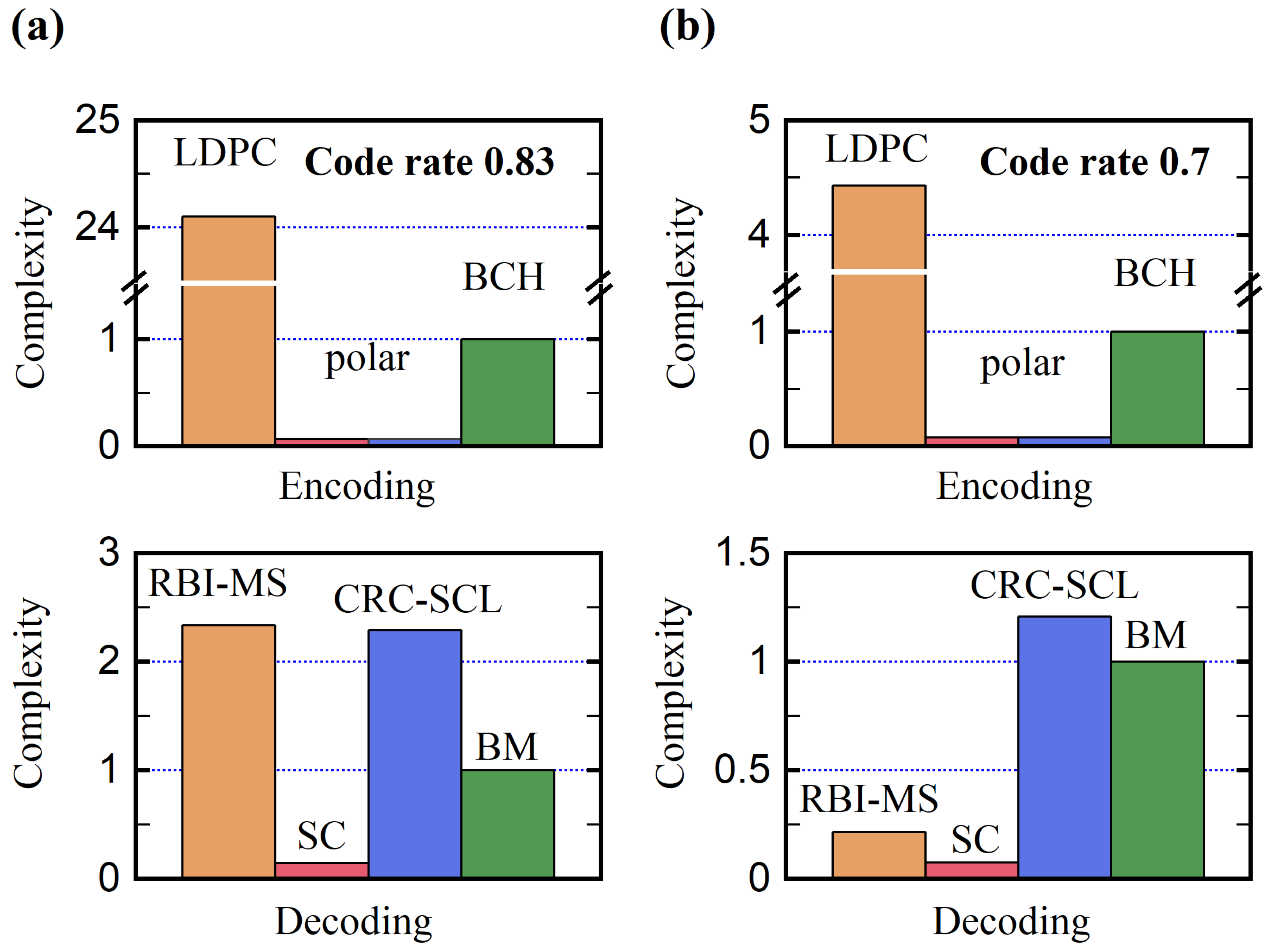
Commercial memory products require ECC schemes with high code rates and low-complexity encoders and decoders. Since complexity is correlated with P, T, and A of the read circuits, the choice of encoder and decoder schemes also depends on the margin offered by the high-density STT-MRAM array in comparison to SRAM. Table 3 lists the encoding and decoding complexities for the BCH, LDPC, and polar codes [22,28,41]. The corresponding encoding and decoding complexities at different code rates are compared in Figure 6a,b. Given N and t, the complexity of the BM decoding algorithm remains constant for the specified code rate. Therefore, the complexities shown in Figure 6a,b were normalized by that of the BCH. When the code rate is 0.83, the encoding complexity of the polar code is 1/17th of BCH, and the decoding complexity of the SC decoder is 1/7th of BM. When the code rate is 0.7, the decoding complexity of the former is 1/13th of BM.
Table 3.
The complexity of different ECC decoding algorithms †.
Figure 6.
The encoding complexities (upper, normalized to BCH code ) and the decoding complexities (lower, normalized to BM) are presented for code rates of (a) 0.83 and (b) 0.7. Here, T = 27 °C, and the corresponding word lengths are shown in Table 2.
5. Conclusions
We implemented 2-bit channel quantization to improve read accuracy in low-RM STT-MRAM. The trade-offs between the overall improvement in read accuracy and the area, power consumption, and latency of the 2-bit quantizers have been investigated. By using these 2-bit quantizers along with an R-based threshold set, polar codes, and SC decoders, 2-bit channel quantization can be achieved with minimal encoding/decoding complexity, while maintaining high read accuracy for short-code-length applications, such as lower-level caches.
Author Contributions
Conceptualization, Y.Y. and S.W.; methodology, Y.Y. and Y.L.; software, Y.Y.; validation, Y.Y., Y.L. and P.C.; formal analysis, Y.Y.; investigation, Y.Y. and Y.L.; resources, S.W. and P.C.; data curation, Y.L. and P.C.; writing—original draft preparation, Y.Y.; writing—review and editing, Y.Y., P.C. and S.W.; visualization, Y.Y. and Y.L.; supervision, S.W.; project administration, S.W.; funding acquisition, S.W. All authors have read and agreed to the published version of the manuscript.
Funding
This research was funded by National Natural Science Foundation of China grant number 62474044.
Data Availability Statement
The data that support the findings of this study are available from the corresponding author upon reasonable request.
Conflicts of Interest
Author Yitong Lai was employed by the company Fujian Jinhua Integrated Circuit Co., Ltd. The remaining authors declare that the research was conducted in the absence of any commercial or financial relationships that could be construed as a potential conflict of interest.
References
- Xiao, K.; Wan, J.; Xie, H.; Zhu, Y.; Tian, T.; Zhang, W.; Chen, Y.; Zhang, J.; Zhou, L.; Dai, S.; et al. High performance Si-MoS2 heterogeneous embedded DRAM. Nat. Commun. 2024, 15, 9782. [Google Scholar] [CrossRef] [Scilit] [PubMed]
- Gallagher, W.; Chien, E.; Chiang, T.W.; Huang, J.C.; Shih, M.C.; Wang, C.; Weng, C.H.; Chen, S.; Bair, C.; Lee, G.; et al. 22 nm STT-MRAM for reflow and automotive uses with high yield, reliability, and magnetic immunity and with performance and shielding options. In Proceedings of the 2019 IEEE International Electron Devices Meeting (IEDM), San Francisco, CA, USA, 7–11 December 2019; IEEE: Piscataway, NJ, USA, 2019; pp. 2–7. [Google Scholar] [CrossRef] [Scilit]
- Jahannia, B.; Ghasemi, S.A.; Farbeh, H. Multi-retention STT-MRAM architectures for IoT: Evaluating the impact of retention levels and memory mapping schemes. IEEE Access 2024, 12, 26562–26580. [Google Scholar] [CrossRef] [Scilit]
- Dieny, B.; Prejbeanu, I.L.; Garello, K.; Gambardella, P.; Freitas, P.; Lehndorff, R.; Raberg, W.; Ebels, U.; Demokritov, S.O.; Akerman, J.; et al. Opportunities and challenges for spintronics in the microelectronics industry. Nat. Electron. 2020, 3, 446–459. [Google Scholar] [CrossRef] [Scilit]
- Wang, Y.; Cai, H.; de Barros Naviner, L.A.; Zhang, Y.; Zhao, X.; Deng, E.; Klein, J.O.; Zhao, W. Compact model of dielectric breakdown in spin-transfer torque magnetic tunnel junction. IEEE Trans. Electron Devices 2016, 63, 1762–1767. [Google Scholar] [CrossRef] [Scilit]
- Alzate, J.; Arslan, U.; Bai, P.; Brockman, J.; Chen, Y.J.; Das, N.; Fischer, K.; Ghani, T.; Heil, P.; Hentges, P.; et al. 2 MB array-level demonstration of STT-MRAM process and performance towards L4 cache applications. In Proceedings of the 2019 IEEE International Electron Devices Meeting (IEDM), San Francisco, CA, USA, 7–11 December 2019; IEEE: Piscataway, NJ, USA, 2019; pp. 2–4. [Google Scholar] [CrossRef] [Scilit]
- Nakayama, M.; Oikawa, S.; Kamata, C.; Toko, M.; Itai, S.; Takashima, R.; Sugiyama, H.; Fukuda, K.; Koike, T.; Saitoh, M.; et al. 14 nm High-Performance MTJ with Accelerated STT-Switching and High-Retention Doped Co-Pt Alloy Storage Layer for 1Znm MRAM. In Proceedings of the 2023 International Electron Devices Meeting (IEDM), San Francisco, CA, USA, 9–13 December 2023; IEEE: Piscataway, NJ, USA, 2023; pp. 1–4. [Google Scholar] [CrossRef] [Scilit]
- Honjo, H.; Nishioka, K.; Miura, S.; Naganuma, H.; Watanabe, T.; Nasuno, T.; Tanigawa, T.; Noguchi, Y.; Inoue, H.; Yasuhira, M.; et al. 25 nm iPMA-type Hexa-MTJ with Solder Reflow Capability and. In Proceedings of the 2022 International Electron Devices Meeting (IEDM), San Francisco, CA, USA, 3–7 December 2022; IEEE: Piscataway, NJ, USA, 2022; pp. 10–13. [Google Scholar] [CrossRef] [Scilit]
- Hu, G.; Lauer, G.; Sun, J.; Hashemi, P.; Safranski, C.; Brown, S.; Buzi, L.; Edwards, E.; D’Emic, C.; Galligan, E.; et al. 2X reduction of STT-MRAM switching current using double spin-torque magnetic tunnel junction. In Proceedings of the 2021 IEEE International Electron Devices Meeting (IEDM), San Francisco, CA, USA, 11–16 December 2021; IEEE: Piscataway, NJ, USA, 2021; pp. 2–5. [Google Scholar] [CrossRef] [Scilit]
- Cai, H.; Bian, Z.; Hou, Y.; Zhou, Y.; Guo, Y.; Tian, X.; Liu, B.; Si, X.; Wang, Z.; Yang, J.; et al. 33.4 A 28nm 2Mb STT-MRAM computing-in-memory macro with a refined bit-cell and 22.4-41.5 TOPS/W for AI inference. In Proceedings of the 2023 IEEE International Solid-State Circuits Conference (ISSCC), San Francisco, CA, USA, 19–23 February 2023; IEEE: Piscataway, NJ, USA, 2023; pp. 500–502. [Google Scholar] [CrossRef] [Scilit]
- Carpenter, R.; Kim, W.; Sankaran, K.; Ao, N.; Chroud, M.B.; Kumar, A.; Trovato, A.; Pourtois, G.; Couet, S.; Kar, G. Demonstration of a Free-layer Developed With Atomistic Simulations Enabling BEOL Compatible VCMA-MRAM with a Coefficient ≥ 100 fJ/Vm. In Proceedings of the 2021 IEEE International Electron Devices Meeting (IEDM), San Francisco, CA, USA, 11–16 December 2021; IEEE: Piscataway, NJ, USA, 2021; pp. 16–17. [Google Scholar] [CrossRef] [Scilit]
- Suhail, H.; He, H.; Yang, J.; Shu, Q.; Wang, C.Y.; Yang, S.Y.; Hsin, Y.C.; Shih, C.Y.; Lee, H.H.; Wu, D.; et al. The First CMOS-Integrated Voltage-Controlled MRAM with 0.7 ns Switching Time. In Proceedings of the 2023 International Electron Devices Meeting (IEDM), San Francisco, CA, USA, 9–13 December 2023; IEEE: Piscataway, NJ, USA, 2023; pp. 1–4. [Google Scholar] [CrossRef] [Scilit]
- Natsui, M.; Suzuki, D.; Tamakoshi, A.; Watanabe, T.; Honjo, H.; Koike, H.; Nasuno, T.; Ma, Y.; Tanigawa, T.; Noguchi, Y.; et al. A 47.14-μW 200-MHz MOS/MTJ-Hybrid Nonvolatile Microcontroller Unit Embedding STT-MRAM and FPGA for IoT Applications. IEEE J.-Solid-State Circuits 2019, 54, 2991–3004. [Google Scholar] [CrossRef] [Scilit]
- Wei, L.; Alzate, J.G.; Arslan, U.; Brockman, J.; Das, N.; Fischer, K.; Ghani, T.; Golonzka, O.; Hentges, P.; Jahan, R.; et al. 13.3 A 7 Mb STT-MRAM in 22FFL FinFET technology with 4ns read sensing time at 0.9 V using write-verify-write scheme and offset-cancellation sensing technique. In Proceedings of the 2019 IEEE International Solid-State Circuits Conference-(ISSCC), San Francisco, CA, USA, 17–21 February 2019; IEEE: Piscataway, NJ, USA, 2019; pp. 214–216. [Google Scholar] [CrossRef] [Scilit]
- Nguyen, V.D.; Talmelli, G.; Monteiro, M.G.; Palomino, A.; Kateel, V.; Giuliano, D.; Van Beek, S.; Vander Meeren, N.; Vergel, N.F.; Wostyn, K.; et al. Achieving 1 ppm Write-Error Rate in SOT-MRAM with Synthetic Antiferromagnetic Free Layer. In Proceedings of the 2024 IEEE International Electron Devices Meeting (IEDM), San Francisco, CA, USA, 7–11 December 2024; IEEE: Piscataway, NJ, USA, 2024; pp. 1–4. [Google Scholar] [CrossRef] [Scilit]
- Liu, E.; Yang, W.; Zhou, K.; Gao, Y.; Ji, Z.; Zeng, D.; Wang, M.; Li, Q.; Xi, Y.; Yang, D.; et al. A Novel Channel-Less SOT-MRAM with 115% TMR, 2 ns Switching, and High Bit Yield (>99.9%). In Proceedings of the 2024 IEEE International Electron Devices Meeting (IEDM), San Francisco, CA, USA, 7–11 December 2024; IEEE: Piscataway, NJ, USA, 2024; pp. 1–4. [Google Scholar] [CrossRef] [Scilit]
- Vander Meeren, N.; Van Beek, S.; Monteiro, M.; Garcia-Redondo, F.; Chatterjee, J.; Kumar, A.; Wostyn, K.; Couet, S.; Verbauwhede, I. Magnetic Immunity of STT-MRAM: External Magnetic Field Orientation Impact on Writing Reliability. In Proceedings of the 2024 IEEE International Electron Devices Meeting (IEDM), San Francisco, CA, USA, 7–11 December 2024; IEEE: Piscataway, NJ, USA, 2024; pp. 1–4. [Google Scholar] [CrossRef] [Scilit]
- Khwa, W.S.; Lu, Y.L.; Zhang, S.Q.; Sun, X.; Sarwar, S.S.; Li, Z.; Chen, W.W.; Wu, J.J.; Peng, X.; Akarvardar, K.; et al. MRAM Design-Technology-System Co-Optimization for Artificial Intelligence Edge Devices. In Proceedings of the 2024 IEEE International Electron Devices Meeting (IEDM), San Francisco, CA, USA, 7–11 December 2024; IEEE: Piscataway, NJ, USA, 2024; pp. 1–4. [Google Scholar] [CrossRef] [Scilit]
- Gottwald, M.; Hu, G.; Trouilloud, P.; Rehm, L.; Safranski, C.; Kim, G.; Brown, S.; Bruley, J.; D’Emic, C.; Gunawan, O.; et al. First demonstration of high retention energy barriers and 2 ns switching, using magnetic ordered-alloy-based STT MRAM devices. In Proceedings of the 2024 IEEE Symposium on VLSI Technology and Circuits (VLSI Technology and Circuits), Honolulu, HI, USA, 16–20 June 2024; IEEE: Piscataway, NJ, USA, 2024; pp. 1–2. [Google Scholar] [CrossRef] [Scilit]
- Yasin, F.; Palomino, A.; Kumar, A.; Pica, V.; Van Beek, S.; Talmelli, G.; Nguyen, V.; Cosemans, S.; Crotti, D.; Wostyn, K.; et al. Extremely scaled perpendicular SOT-MRAM array integration on 300 mm wafer. In Proceedings of the 2024 IEEE Symposium on VLSI Technology and Circuits (VLSI Technology and Circuits), Honolulu, HI, USA, 16–20 June 2024; IEEE: Piscataway, NJ, USA, 2024; pp. 1–2. [Google Scholar] [CrossRef] [Scilit]
- Mei, Z.; Cai, K.; Shi, L.; He, X. On channel quantization for spin-torque transfer magnetic random access memory. IEEE Trans. Commun. 2019, 67, 7526–7539. [Google Scholar] [CrossRef] [Scilit]
- Mei, Z.; Cai, K.; Dai, B. Polar codes for spin-torque transfer magnetic random access memory. IEEE Trans. Magn. 2018, 54, 1–5. [Google Scholar] [CrossRef] [Scilit]
- Song, Y.; Lee, J.; Han, S.; Shin, H.; Lee, K.; Suh, K.; Jeong, D.; Koh, G.; Oh, S.; Park, J.; et al. Demonstration of highly manufacturable STT-MRAM embedded in 28 nm logic. In Proceedings of the 2018 IEEE International Electron Devices Meeting (IEDM), San Francisco, CA, USA, 1–5 December 2018; IEEE: Piscataway, NJ, USA, 2018; pp. 12–18. [Google Scholar] [CrossRef] [Scilit]
- Shi, Y.; Oh, S.; Huang, Z.; Lu, X.; Kang, S.H.; Kuzum, D. Performance prospects of deeply scaled spin-transfer torque magnetic random-access memory for in-memory computing. IEEE Electron Device Lett. 2020, 41, 1126–1129. [Google Scholar] [CrossRef] [Scilit]
- Na, T.; Kang, S.H.; Jung, S.O. STT-MRAM sensing: A review. IEEE Trans. Circuits Syst. II Express Briefs 2020, 68, 12–18. [Google Scholar] [CrossRef] [Scilit]
- Xu, G.; Hu, Y.; Feng, D.; He, W.; Huang, J. CodePM: Parity-Based Crash Consistency for Log-Free Persistent Transactional Memory. IEEE Trans.-Comput.-Aided Des. Integr. Circuits Syst. 2024, 44, 1717–1730. [Google Scholar] [CrossRef] [Scilit]
- Lin, K.F.; Noguchi, H.; Shih, Y.C.; Yuh, P.F.; Lee, Y.J.; Chang, T.C.; Huang, S.P.; Lin, Y.F.; Lee, C.Y.; Huang, Y.H.; et al. 15.9 A 16 nm 16 Mb embedded STT-MRAM with a 20 ns write time, a 1012 write endurance and integrated margin-expansion schemes. In Proceedings of the 2024 IEEE International Solid-State Circuits Conference (ISSCC), San Francisco, CA, USA, 18–22 February 2024; IEEE: Piscataway, NJ, USA, 2024; Volume 67, pp. 292–294. [Google Scholar] [CrossRef] [Scilit]
- Girard, P.; Cheng, Y.; Virazel, A.; Zhao, W.; Bishnoi, R.; Tahoori, M.B. A survey of test and reliability solutions for magnetic random access memories. Proc. IEEE 2020, 109, 149–169. [Google Scholar] [CrossRef] [Scilit]
- Zhang, L.; Ma, Y.; Endoh, T. Efficient BCH code encoding and decoding algorithm with divisor-distance-based polynomial division for STT-MRAM. IEEE Trans. Magn. 2022, 59, 3400508. [Google Scholar] [CrossRef] [Scilit]
- Wu, B.; Zhang, B.; Cheng, Y.; Wang, Y.; Liu, D.; Zhao, W. An adaptive thermal-aware ECC scheme for reliable STT-MRAM LLC design. IEEE Trans. Very Large Scale Integr. (Vlsi) Syst. 2019, 27, 1851–1860. [Google Scholar] [CrossRef] [Scilit]
- Sayed, N.; Bishnoi, R.; Tahoori, M.B. Fast and reliable STT-MRAM using nonuniform and adaptive error detecting and correcting scheme. IEEE Trans. Very Large Scale Integr. (Vlsi) Syst. 2019, 27, 1329–1342. [Google Scholar] [CrossRef] [Scilit]
- Huang, K.; Ning, N.; Lian, Y. Optimization scheme to minimize reference resistance distribution of spin-transfer-torque MRAM. IEEE Trans. Very Large Scale Integr. (Vlsi) Syst. 2013, 22, 1179–1182. [Google Scholar] [CrossRef] [Scilit]
- Cai, K.; Immink, K. A cascaded channel model and hybrid decoding for spin-torque transfer magnetic random access memory (STT-MRAM). In Proceedings of the 2017 IEEE International Magnetics Conference (INTERMAG), Dublin, Ireland, 24–28 April 2017; IEEE: Piscataway, NJ, USA, 2017; p. 1. [Google Scholar] [CrossRef] [Scilit]
- Siddanath, R.S.; Gupta, M.; Das, S.K.; Prasad, G.; Goswami, M.; Kandpal, K. A data-driven self-terminating write circuit with enhanced reliability for STT-MRAM using MUX logic. Microelectron. Reliab. 2026, 177, 116006. [Google Scholar] [CrossRef] [Scilit]
- Yuan, L.; Chen, J.; Zhuo, P.; Wang, S. A high reliability, multi-bit parallel readout in-memory computing scheme based on STT-MRAM. Microelectron. Comput. 2022, 39, 119–126. [Google Scholar] [CrossRef]
- Mei, Z.; Cai, K.; Shi, L.; Li, J. Quantization design for resistive memories with multiple reads. IEEE Commun. Lett. 2023, 27, 822–826. [Google Scholar] [CrossRef] [Scilit]
- Mei, Z.; Cai, K.; Shi, L. Information theoretic bounds based channel quantization design for emerging memories. In Proceedings of the 2018 IEEE Information Theory Workshop (ITW), Guangzhou, China, 25–29 November 2018; IEEE: Piscataway, NJ, USA, 2018; pp. 1–5. [Google Scholar] [CrossRef] [Scilit]
- Rossi, D.; Timoncini, N.; Spica, M.; Metra, C. Error correcting code analysis for cache memory high reliability and performance. In Proceedings of the 2011 Design, Automation & Test in Europe, Grenoble, France, 14–18 March 2011; IEEE: Piscataway, NJ, USA, 2011; pp. 1–6. [Google Scholar] [CrossRef] [Scilit]
- Mittal, S.; Inukonda, M.S. A survey of techniques for improving error-resilience of DRAM. J. Syst. Archit. 2018, 91, 11–40. [Google Scholar] [CrossRef] [Scilit]
- Patel, M.; Kim, J.S.; Shahroodi, T.; Hassan, H.; Mutlu, O. Bit-exact ECC recovery (BEER): Determining DRAM on-die ECC functions by exploiting DRAM data retention characteristics. In Proceedings of the 2020 53rd Annual IEEE/ACM International Symposium on Microarchitecture (MICRO), Grenoble, France, 14–18 March 2020; IEEE: Piscataway, NJ, USA, 2020; pp. 282–297. [Google Scholar] [CrossRef] [Scilit]
- Cai, K.; Qin, Z.; Chen, B. Channel capacity and soft-decision decoding of LDPC codes for spin-torque transfer magnetic random access memory (STT-MRAM). In Proceedings of the 2013 International Conference on Computing, Networking and Communications (ICNC), San Diego, CA, USA, 28–31 January 2013; IEEE: Piscataway, NJ, USA, 2013; pp. 550–554. [Google Scholar] [CrossRef] [Scilit]

Disclaimer/Publisher’s Note: The statements, opinions and data contained in all publications are solely those of the individual author(s) and contributor(s) and not of MDPI and/or the editor(s). MDPI and/or the editor(s) disclaim responsibility for any injury to people or property resulting from any ideas, methods, instructions or products referred to in the content. |
© 2026 by the authors. Licensee MDPI, Basel, Switzerland. This article is an open access article distributed under the terms and conditions of the Creative Commons Attribution (CC BY) license.