


Abstract
In this study, the indium (In) composition in amorphous indium gallium zinc oxide (a-IGZO) thin films was systematically varied from 33% to 84% using a sol–gel process. Subsequently, aluminum/IGZO/aluminum (Al/IGZO/Al) metal–semiconductor–metal (MSM) UV photodetectors were fabricated to investigate the influence of composition on the structural, optical, and photoelectric properties. The results indicate that all films maintain an amorphous structure despite the increasing In content, while the ratio of oxygen vacancies, Ovac/(M-O + Ovac), rises from 36% to 52%. Concurrently, the optical bandgap decreases from 2.92 eV to 2.32 eV. Under a bias of 20 V, the dark current increases from 2.11 × 10⁻⁹ A to 1.90 × 10⁻⁵ A as the In content rises. When illuminated by a 360 nm LED with a power density of 8.6 mW/cm2, the device with 60% In exhibits a photocurrent-to-dark-current ratio of approximately 104, a responsivity of 19.45 A/W, and a specific detectivity of 8.19 × 10¹² Jones. The response time and recovery time of this device are 39.8 s and 577.4 s, respectively. These findings reveal a competitive relationship between enhanced optical absorption and defect generation induced by In composition, providing valuable guidance for the performance optimization of a-IGZO UV photodetectors through compositional engineering.
1. Introduction
Ultraviolet (UV) photodetectors have garnered significant attention due to their critical applications in environmental monitoring, flame detection, biomedical imaging, and space communication [1,2,3,4]. Conventional UV photodetectors are predominantly based on III–V or wide-bandgap single-crystal semiconductors. Although these materials demonstrate exceptional performance, their high costs and intricate fabrication processes hinder large-scale applications. In recent years, amorphous oxide semiconductors (AOSs) have been widely adopted in flexible electronics, electromagnetic shielding and sensing technologies due to their low-temperature fabrication capabilities, excellent large-area uniformity and compatibility with existing microelectronic processes. They have also become a promising alternative material in the field of ultraviolet light detection [1,5,6,7]. A-IGZO is regarded as a highly promising material for ultraviolet (UV) photodetection due to its wide bandgap, high electron mobility, and exceptional chemical stability. Furthermore, its high optical transparency, low-temperature processability, and excellent scalability have significantly increased interest in this amorphous oxide semiconductor for UV detection applications [8,9,10]. Among various device architectures, the metal-semiconductor-metal (MSM) structure has been widely utilized in IGZO-based UV photodetectors due to its straightforward fabrication process and rapid response characteristics. Song et al. reported a low-voltage IGZO field-effect ultraviolet photodiode, demonstrating that the a-IGZO material exhibits excellent spectral selectivity in the ultraviolet band, while its response is extremely low in the visible light region [11]. Previous studies have shown that factors such as annealing temperature, oxygen partial pressure, film thickness, and defect engineering can substantially influence the optoelectronic performance of these devices [12]. For instance, Li et al. fabricated a-IGZO photodetectors with varying film thicknesses, achieving a photo-to-dark current ratio of approximately 23,924 for a 115 nm thick film under 365 nm UV illumination with an intensity of 17,102 mW/m2 [13]. Yu et al. reported a UV photodetector based on a thin-film transistor structure, which demonstrated a high responsivity of 984 A/W, a photo-to-dark current ratio of 3.5 × 10⁷, and a detectivity of 3.3 × 10¹⁴ Jones under 320 nm illumination [14]. These performances are significantly superior to many previously reported IGZO photodetectors. In recent years, significant advancements have been made in IGZO-based ultraviolet (UV) photodetectors through device structure engineering and interface modulation. For instance, NiO/IGZO heterojunction photodetectors have exhibited self-powered operation and rapid photoresponse characteristics due to efficient carrier separation at the p-n junction interface [15]. Additionally, chemically treated IGZO phototransistors have been shown to effectively suppress persistent photoconductivity and enhance UV selectivity [16]. Furthermore, heterostructure devices, such as p-GaN/IGZO and β-Ga2O3/IGZO, have been investigated to improve carrier transport and responsivity through band alignment and interface engineering [17,18]. Despite these advancements, most existing studies primarily concentrate on heterostructure design, defect regulation, and process optimization, while the intrinsic influence of metal composition in IGZO on its electronic structure and photodetection performance remains inadequately understood. In particular, systematic investigations into how In composition affects the band structure, defect states, and optoelectronic properties of IGZO are still relatively scarce. From the perspective of band structure, the conduction band of IGZO is predominantly derived from In 5s orbitals, whereas Ga and Zn serve to suppress excessive carrier concentration and enhance structural stability [19,20]. Cadis Adrian-Ionut et al. changed the optical bandgap of the material by doping [21]. Consequently, variations in In content are expected to directly modulate the conduction band minimum, carrier effective mass, and electron transport behavior [22,23]. Nevertheless, systematic studies investigating the influence of In composition on the band structure and photoelectric performance of IGZO UV photodetectors remain limited. In particular, the intrinsic relationship between In composition and device performance optimization for amorphous IGZO thin films prepared via the sol–gel method has yet to be clearly elucidated.
Compared with vacuum deposition techniques, the sol–gel method offers advantages such as low cost, large-area fabrication, and excellent compositional tunability. However, the performance of thin-film devices is significantly influenced by material composition, defect control, and the fabrication process. These factors continue to pose key challenges for large-scale and cost-effective applications [24]. Therefore, this study aims to develop low-cost, large-area UV photodetectors by employing the sol–gel method to prepare amorphous IGZO thin films with varying indium compositions and fabricating MSM structured devices. By systematically tuning the In content in IGZO, we investigate the influence of In composition on the band structure, optical bandgap, defect states, and photoelectric response characteristics of the devices in detail. Through a combination of structural characterization, chemical state analysis, and optoelectronic measurements, we reveal the synergistic mechanism of conduction-band modulation and oxygen-related defect formation induced by the In composition. Our results clarify the critical role of In composition in optimizing the performance of IGZO UV photodetectors and provide new insights into compositional engineering for amorphous oxide optoelectronic devices.
2. Materials and Methods
All chemical reagents utilized in this study were of analytical grade or higher, including indium nitrate hydrate (In(NO3)3·xH2O, AR), gallium nitrate hydrate (Ga(NO3)3·xH2O, AR), zinc nitrate hydrate (Zn(NO3)2·xH2O, AR), 2-methoxyethanol (AR, 99.99%), and polyethylene glycol (PEG, average molecular weight ≈ 10,000). Additionally, ethanol, acetone, and deionized water were used. The above reagents are all provided by Shanghai Titan Technology Co., Ltd., Shanghai, China. An aluminum sputtering target with a purity of 99.99% was employed for electrode deposition. This target material was purchased from Dongming New Materials, Shijiazhuang, China. Silicon/silicon dioxide (Si/SiO2) substrates featuring a 270 nm SiO2 layer were utilized for device fabrication, while films for X-ray diffraction (XRD) and UV–visible spectroscopy measurements were deposited on quartz glass substrates to mitigate optical interference from the silicon substrate.
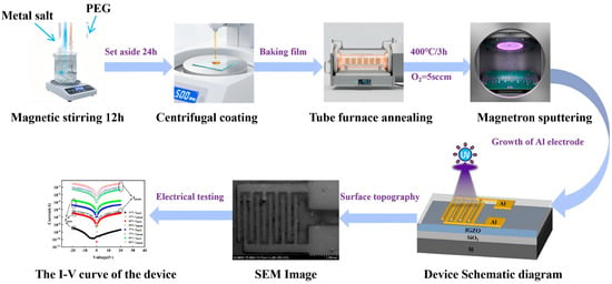
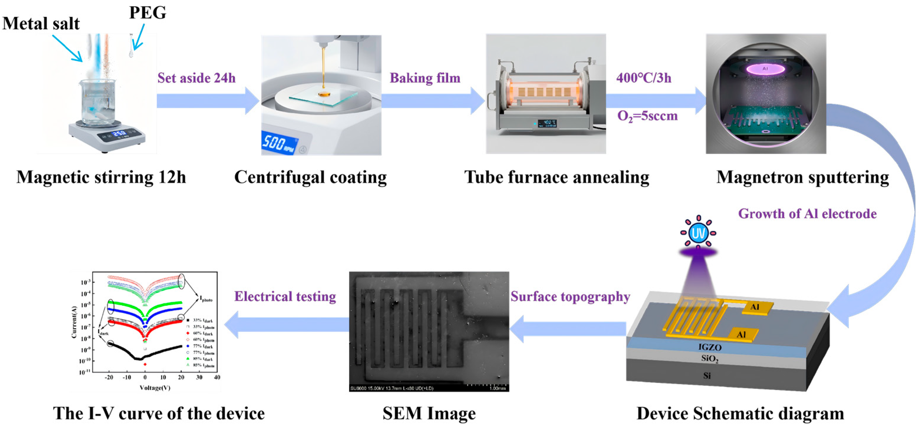
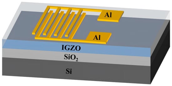
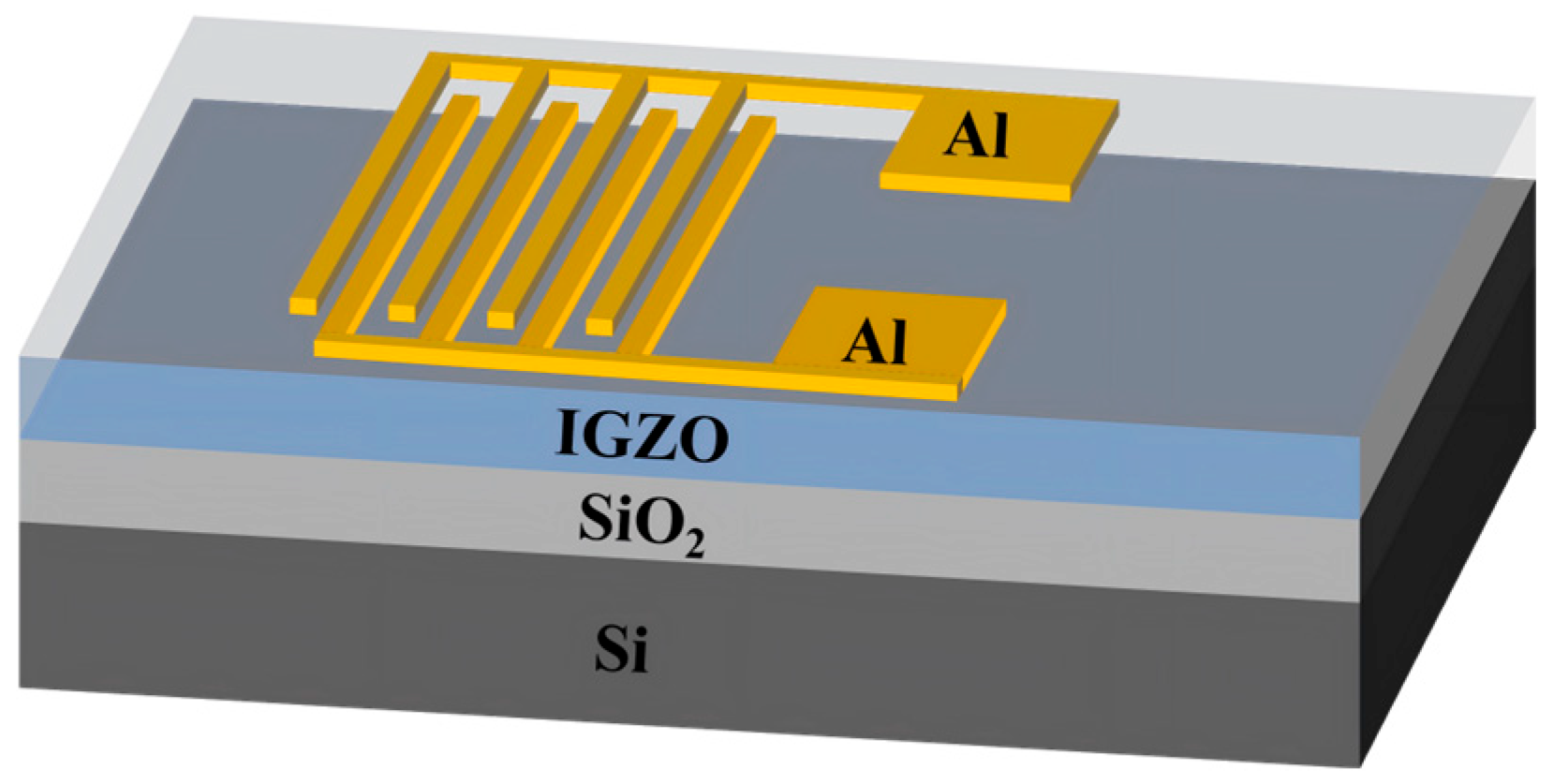
The synthetic route is shown in Figure 1. Indium nitrate hydrate, gallium nitrate hydrate, and zinc nitrate hydrate were individually dissolved in 2-methoxyethanol to prepare metal salt stock solutions with a concentration of 0.2 M. Each solution was magnetically stirred for 4 h to ensure complete dissolution. The three stock solutions were then mixed according to the designed indium composition ratios (33 at.%, 60 at.%, 77 at.%, and 84 at.%) and stirred for an additional 12 h to obtain homogeneous and stable IGZO precursor solutions. Polyethylene glycol (PEG) was added as a film-forming additive and complexing agent, followed by heating in a 40 °C water bath for 1 h to promote chelation and enhance solution stability. The resulting precursor solutions were aged at room temperature for 24 h before use. Prior to film deposition, the Si/SiO2 substrates were thoroughly cleaned. The substrates were ultrasonically cleaned sequentially in acetone, ethanol, and deionized water for 15 min each to remove organic contaminants and particulates. After drying with high-purity nitrogen, the substrates were treated in a UV-ozone cleaner for 30 min to eliminate residual organics and enhance surface hydrophilicity, thereby improving the wettability of the precursor solution. IGZO thin films were deposited by spin coating. Approximately 40 μL of the precursor solution was deposited onto the substrate and spin-coated at 5500 rpm for 15 s to form a uniform film. The coated films were immediately pre-baked on a hot plate at 120 °C for 30 min to remove solvent and promote gel formation. Subsequently, the samples were annealed in a tube furnace at 400 °C for 3 h under an O2 flow of 5 sccm. This annealing step removed residual organics and facilitated the formation of a metal-oxygen network, stabilizing the amorphous structure. After process optimization, amorphous IGZO films with a thickness of approximately about 50 nm were obtained for subsequent morphology, structural, chemical-state, and optoelectronic characterizations. The photodetectors utilized an MSM structure, as illustrated in Figure 2 Aluminum interdigital electrodes were deposited on the IGZO films using magnetron sputtering. The Al electrodes were deposited via DC magnetron sputtering at a power of 100 W, a working pressure of 0.5 Pa, an Ar flow rate of 40 sccm, a base pressure of better than 3.2 × 10⁻⁴ Pa, and a deposition time of 600 s. The electrode patterns were defined using a metal shadow mask. Both the electrode finger width and spacing measured 0.1 mm, while the finger length was 2 mm, establishing an Al/IGZO/Al configuration for photodetection measurements. To ensure that the performance differences among devices due to different In contents are mainly attributed to the variations in indium content, we strictly controlled the preparation and testing conditions. The film thickness was regulated by maintaining a consistent spin-coating speed of 5500 rpm and a precursor concentration of 0.2 M. All samples underwent annealing under identical conditions, the electrodes were deposited using DC magnetron sputtering with uniform parameters, and all optoelectronic measurements were conducted under the same conditions.
Figure 1.
The technical roadmap for fabricating IGZO MSM thin-film optoelectronic devices.
Figure 2.
The structure diagram of the a-IGZO MSM photodetector.
The surface morphology of the films and devices was examined using a field-emission scanning electron microscope (SEM, SU8600, Hitachi, Tokyo, Japan). The crystallographic structure was analyzed through X-ray diffraction (XRD, D8 ADVANCE, Bruker, Ettlingen, Germany) employing Cu Kα radiation. The elemental composition and distribution of the films were characterized using energy-dispersive X-ray spectroscopy (EDS) with an Xplore detector (Oxford Instruments, Oxford, UK). The chemical states and elemental valence of the film surfaces were characterized using X-ray photoelectron spectroscopy (XPS, K-Alpha, Thermo Scientific, Waltham, MA, USA). The optical transmittance spectra of the IGZO films were measured with a UV–vis–NIR spectrophotometer (UV-3600i Plus, Shimadzu, Kyoto, Japan). Finally, the electrical and photoelectrical properties of the devices were systematically evaluated on a probe station using a source meter (Keithley 2400, Keithley, Cleveland, OH, USA).
3. Results
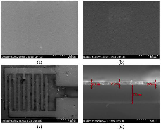
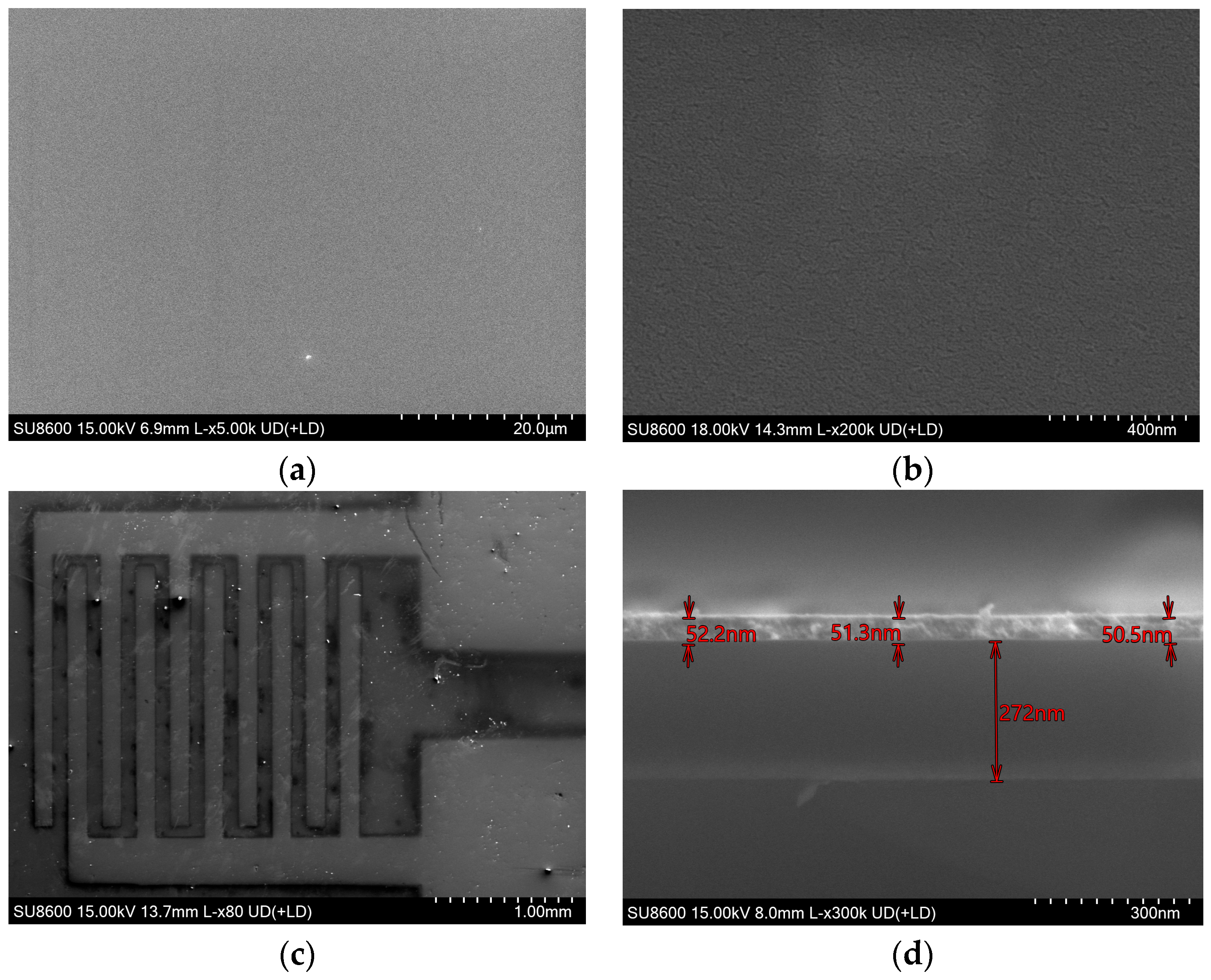
As illustrated in Figure 3a,b, the surface morphology of the IGZO thin film prepared using the sol–gel method is depicted. The film exhibits a continuous, dense, and uniform surface morphology. No cracks, pinholes, or noticeable particle agglomerations are observed within the examined scale, indicating that the precursor solution possesses favorable wettability and spreading characteristics. Furthermore, annealing at 400 °C promotes the formation of a structurally stable and dense oxide network. At higher magnification, no distinct grain boundaries or well-defined crystal facets are observed, suggesting that the film exhibits a typical amorphous structure. This observation aligns with previously reported amorphous IGZO films [6] and is further corroborated by the absence of distinct diffraction peaks in the subsequent XRD analysis. As shown in Figure 3c, the morphology of the MSM photodetector fabricated on the IGZO film is presented. The deposited Al interdigital electrodes display well-defined, regular, and continuous geometrical features. A tight interface between the Al electrodes and the IGZO film is observed, and no significant delamination, peeling, or interface degradation caused by metal diffusion is detected, indicating that the magnetron sputtering process does not induce noticeable structural damage to the film. Additionally, the interdigital electrodes are uniformly arranged with parallel finger structures and consistent spacing, which facilitates the formation of a stable and uniform electric field during device operation, thereby ensuring reliable and reproducible photoresponse characteristics. As shown in Figure 3d, the cross-section of the film is presented, clearly revealing a 270 nm layer of silicon dioxide. The thickness of the IGZO film is approximately 50 nm.
Figure 3.
SEM image of IGZO thin film and device: (a) SEM (×5k) image of the surface of a-IGZO film; (b) SEM (×200k) image of the surface of a-IGZO film; (c) SEM image of IGZO device; (d) SEM image of the IGZO film cross-section.
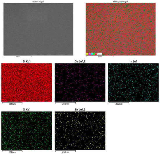
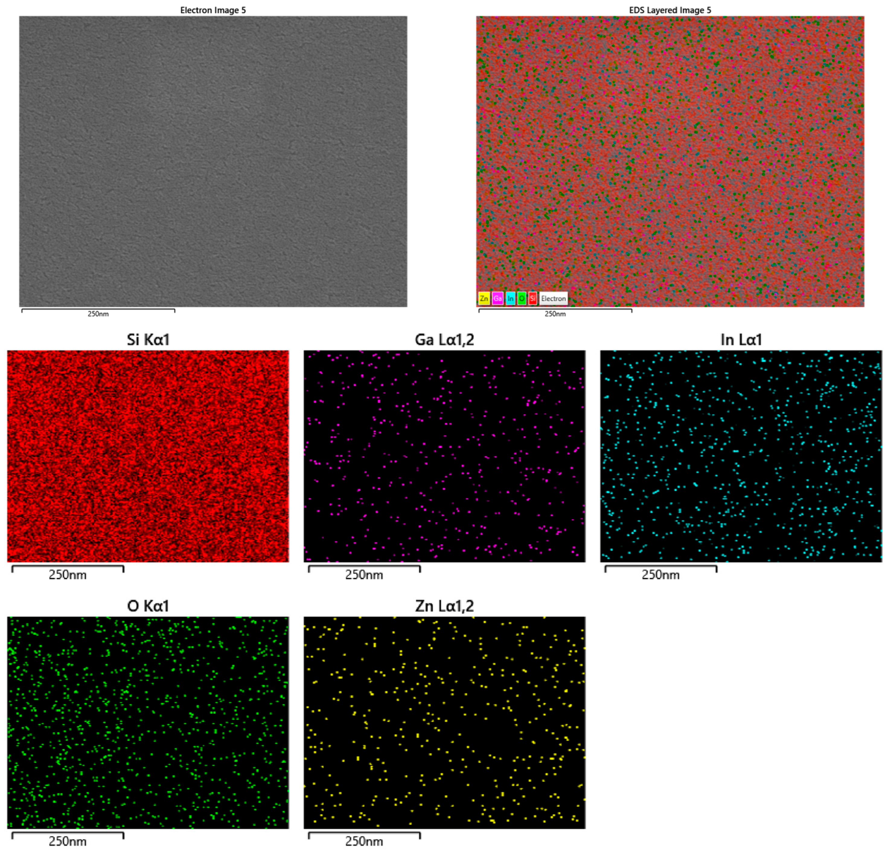
To further confirm the elemental composition and distribution of the IGZO film, an EDS analysis was performed on the sample. As illustrated in Figure 4, the elemental surface scanning results demonstrate that Si, In, Ga, Zn, and O are uniformly distributed across the film surface. Furthermore, there was no notable element enrichment or agglomeration observed, indicating that the prepared IGZO film exhibits excellent compositional uniformity.
Figure 4.
EDS image of the element distribution of the IGZO film.
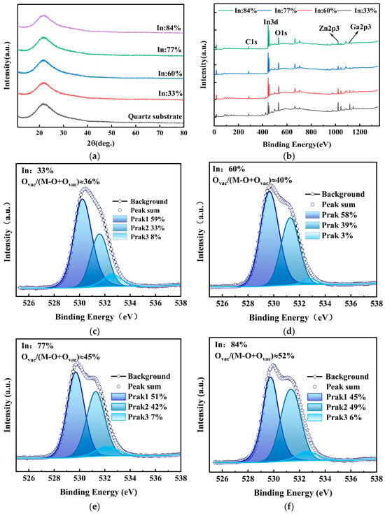
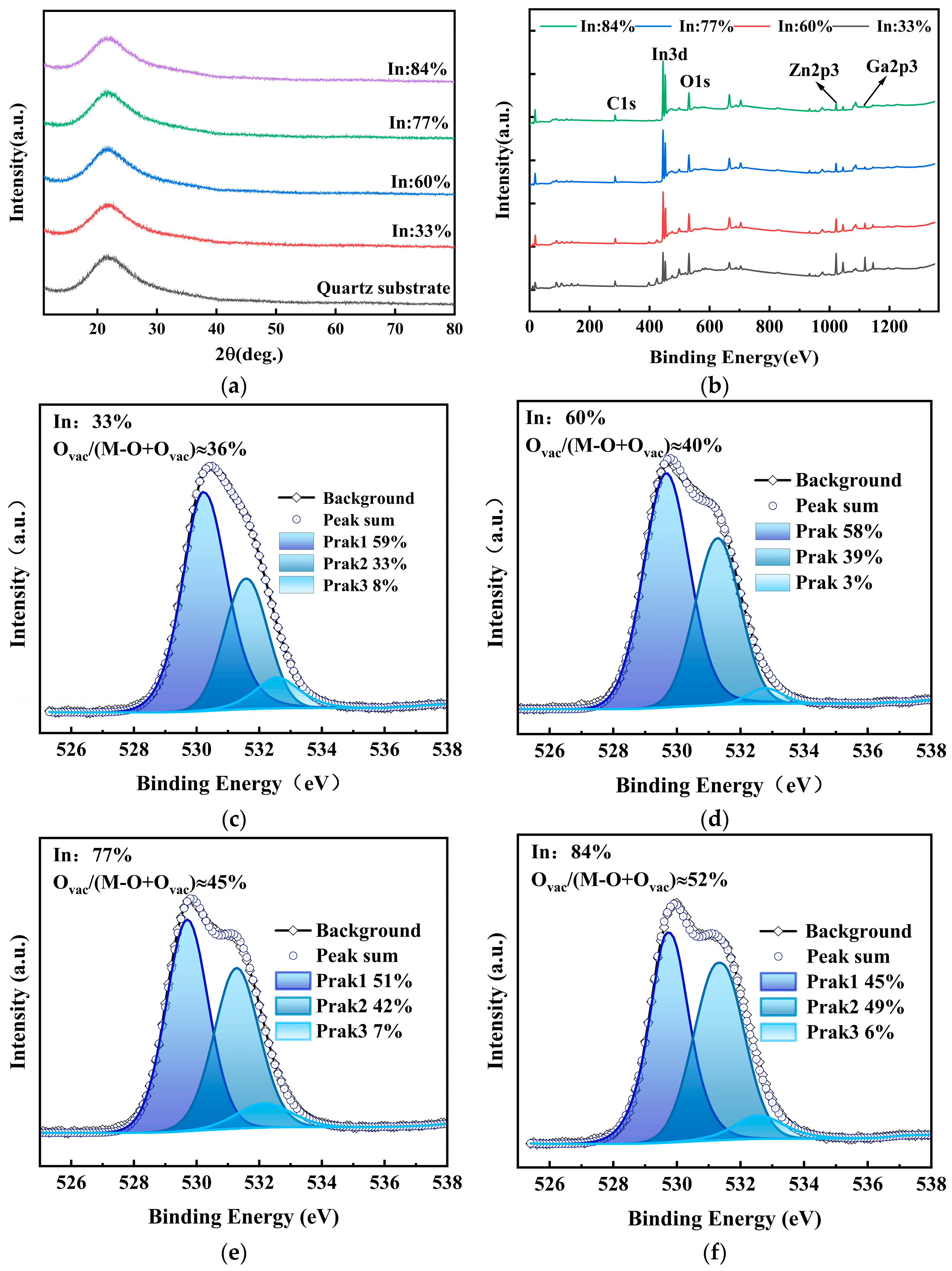
To further investigate the structural characteristics of the films, the X-ray diffraction (XRD) patterns of IGZO films with varying In contents are presented in Figure 5a. No distinct crystalline diffraction peaks are observed within the measured range for all samples; only a broad background signal originating from the substrate is detected. The absence of sharp and characteristic diffraction peaks indicates that the films lack long-range crystalline order and exhibit a typical amorphous structure [25]. Notably, the XRD patterns remain essentially unchanged across different In contents (33%, 60%, 77%, and 84%), suggesting that variations in In composition do not induce crystallization under the current fabrication conditions but primarily influence the electronic structure and defect characteristics of the IGZO films.
Figure 5.
The XRD spectra of amorphous IGZO films and the complete XPS spectra, along with the O 1s sub-spectra of the film surface, are presented as follows: (a) XRD spectra for various indium (In)-component IGZO films; (b) full XPS spectra for different In-component IGZO films; (c) O 1s spectral profile of the IGZO film with 33% In content; (d) O 1s spectral profile of the IGZO film with 60% In content; (e) O 1s spectral profile of the IGZO film with 77% In content; (f) O 1s spectral profile of the IGZO film with 84% In content.
Figure 5b–f presents the X-ray photoelectron spectroscopy (XPS) survey spectra and high-resolution O 1s spectra of IGZO films with varying In compositions. In the survey spectra, characteristic peaks corresponding to In 3d, Ga 2p, Zn 2p, and O 1s are distinctly observed across all samples, alongside a C 1s signal indicative of surface contamination [26]. The absence of additional impurity peaks confirms the high chemical purity of the films. To mitigate the effects of surface charging, all binding energies were calibrated using the C 1s peak at 284.8 eV [26]. As shown in Figure 5c–f, the high-resolution O 1s spectra can be deconvoluted into three components through Gaussian peak fitting. The peak at approximately ~530.0 eV corresponds to lattice oxygen (M-O, where M = In, Ga, and Zn). The component centered around ~531.0 eV is attributed to oxygen atoms located in oxygen-deficient environments, i.e., oxygen atoms in the vicinity of oxygen vacancies, which experience a modified local electronic structure. The peak at approximately ~532.5 eV is assigned to surface-adsorbed oxygen species or hydroxyl groups (-OH) [27]. Quantitative analysis indicates that the ratio of Ovac/(M-O + Ovac) increases systematically with increasing In content, ranging from 33% to 84%, with corresponding values of 36%, 40%, 45%, and 52%, respectively. Concurrently, the relative fraction of lattice oxygen gradually decreases. It is well established that an increase in indium content leads to a corresponding rise in oxygen-related defects. This trend can be rationalized through considerations of chemical bonding and local structural evolution: compared to Ga-O and Zn-O bonds, the In-O bond exhibits lower binding energy and reduced coordination stability. Consequently, a higher In concentration promotes the formation of In-O-In linkages, intensifying local coordination unsaturation and facilitating the generation of Ovac. From a device physics perspective, Ovac typically behaves as shallow donor defects. The incorporation of In not only enhances electron transport pathways but also shifts the position of the Fermi level. Furthermore, defect states associated with Ovac may give rise to band-tail states or intra-gap energy levels, exerting a dual influence-suppressing non-radiative recombination and modulating photogenerated carrier transport. It should be noted that the increase in the oxygen vacancy-related component does not scale linearly with indium concentration. Although indium incorporation tends to promote the formation of oxygen vacancies, the overall defect concentration is governed by multiple factors, including the strong bonding of Ga-O, local structural stability, and defect formation energetics [1,28].
To further evaluate the overall level of residual organic impurities in the IGZO thin films, FTIR analysis was conducted on samples with varying In compositions, with the results presented in Figure S1 of the Supplementary Materials. The FTIR spectra for all samples display a broad absorption band in the range of 3200–3600 cm−1, corresponding to the O-H stretching vibrations of hydrogen-bonded hydroxyl groups [29,30]. The overall intensity of this band is notably weak, indicating that the annealing process at 400 °C for 3 h in an O2 atmosphere effectively removes the majority of organic residues and hydroxyl groups. The weak sharp peak observed at approximately 3750 cm−1 and the doublet in the range of 2300–2400 cm−1 are attributed to residual water vapor and atmospheric CO2, respectively, and are not related to the samples. The 400 °C annealing temperature employed in this work can effectively remove organic residues and form high-quality metal-oxygen networks. However, this high-temperature process is incompatible with the tolerance temperature of most flexible plastic substrates. This limitation restricts the direct application of the sol-gel method IGZO films in the field of flexible ultraviolet detectors.
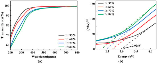
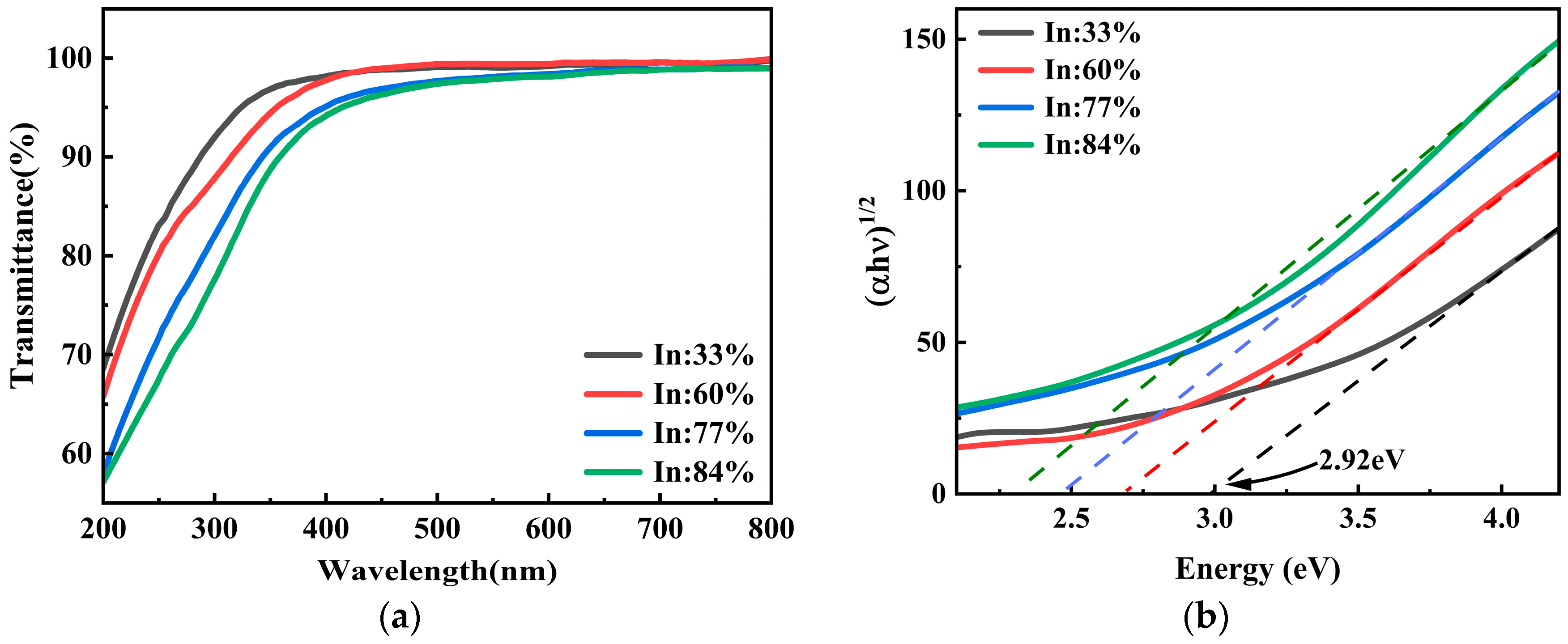
The optical transmittance spectra of IGZO films deposited on quartz substrates are presented in Figure 6a. All samples demonstrate excellent optical transparency in the visible region. After accounting for the substrate contribution, the average transmittance exceeds 90%, which is significantly higher than the typical values reported for most IGZO films in the literature, around 80% [31,32,33]. A closer examination of the absorption edge reveals a slight but systematic redshift in the transmittance spectra with increasing In composition, indicating that the electronic structure of the films is influenced by compositional variation. The optical bandgap (Eg) of the films was estimated using the Tauc relation [34]:
where α is the absorption coefficient, hν is the incident photon energy, and A is a constant. In practice, the absorption coefficient α can be derived from the film thickness (t) and the measured transmittance (T), as described in Equation [35].
Figure 6.
Optical properties of IGZO thin films with different In compositions: (a) optical transmittance spectra measured on quartz substrates; (b) corresponding Tauc plots used for bandgap extraction.
The corresponding Tauc plots are presented in Figure 6b, and linear extrapolation yields bandgap values of 2.92, 2.67, 2.48 and 2.32 eV for films with increasing In content. Notably, all samples exhibit a pronounced absorption edge in the 200–400 nm region. However, the transmittance in this wavelength range gradually decreases with increasing In concentration, indicating enhanced ultraviolet absorption. The redshift of the absorption edge aligns with the gradual narrowing of the bandgap observed from the Tauc analysis. In conjunction with the XPS results, it can be inferred that the proportion of oxygen-related defects increases in samples with higher In content. A higher In concentration weakens the stability of the M-O bonding network, promoting the formation of oxygen-related defects. These defects introduce localized states within the bandgap, effectively narrowing the optical bandgap and enhancing sub-bandgap absorption.
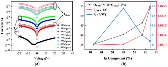
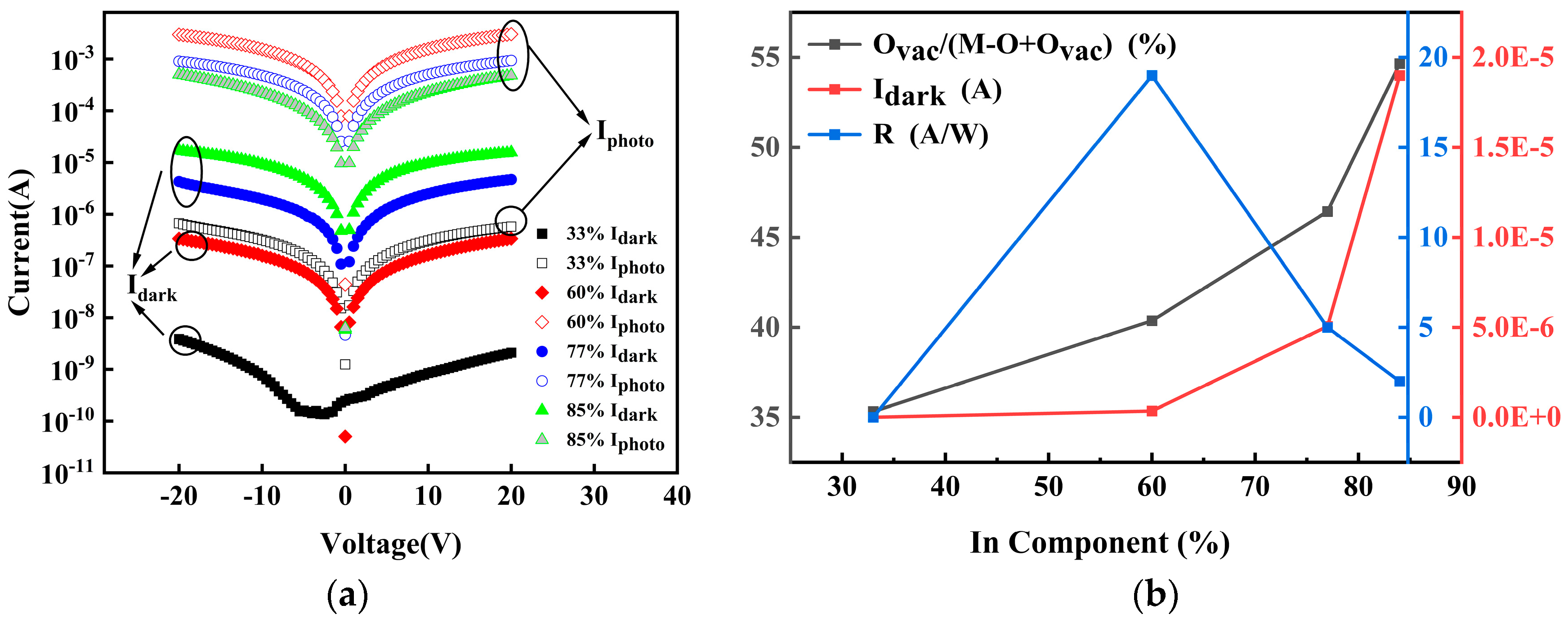
Figure 7a illustrates the I-V characteristics of MSM-type ultraviolet photodetectors fabricated from IGZO films with varying In compositions, illuminated by a 360 nm LED at a power density of 8.6 mW/cm2. The voltage was varied from −20 V to 20 V in increments of 0.5 V. Under the same bias conditions, all devices demonstrated pronounced photoresponse behavior, with photocurrents significantly exceeding the corresponding dark currents, indicating that the IGZO films exhibit high sensitivity to 360 nm ultraviolet light. Under UV illumination, incident photons generate a substantial number of electron-hole pairs in the IGZO layer, which increases the carrier concentration and enhances carrier drift transport, resulting in a marked increase in the measured current. As the applied bias increases, the photocurrent shows an approximately linear dependence on voltage, suggesting that the device behavior in this voltage range is primarily governed by Ohmic conduction and carrier drift transport. Furthermore, we observed that the I–V curve of the In group with 33% Idark content exhibited an unexpected negative change. A possible mechanism for this phenomenon is the capture of charge carriers by surface or deep-level traps, which leads to the formation of spatial charge accumulation. This accumulation generates an intrinsic electric field within the device that opposes the direction of the applied bias, giving rise to a reverse current at low voltages. Such trap-induced reverse current behavior has been reported in metal–semiconductor–metal (MSM) photodetectors and is commonly attributed to space charge effects [36,37].
Figure 7.
(a) The I–V curves of a-IGZO MSM photodetectors in dark and under 360 nm UV illumination. (b) The variation trends of oxygen vacancy ratio, dark current and responsivity of IGZO films under different In compositions.
From the perspective of composition dependence, the photocurrent generally increases with increasing In content; however, the dark current also rises simultaneously, resulting in a non-monotonic variation in the (Iphoto/Idark). This behavior reflects two competing physical processes. On one hand, the increase in In content leads to a reduction in the optical Eg of the IGZO films, which enhances intrinsic absorption at 360 nm and consequently generates more photogenerated carriers, thereby increasing the Iphoto. On the other hand, higher In compositions are typically accompanied by an increased concentration of oxygen-related defects. These defects act as donor-like states that elevate the background electron concentration, leading to an increase in the dark current. Therefore, the influence of In composition on device performance can be fundamentally understood as a dynamic balance between enhanced optical absorption and increased defect density. To quantitatively evaluate the photodetection capability of the device, the responsivity (R) was extracted from the measured photocurrent using the following equation [38]:
Here, P represents the incident optical power, defined as the product of the incident power density and the effective illuminated area of the device. The calculated results indicate that the sample with an In composition of 60% exhibits the highest R. However, when the In content is further increased, the optical absorption of the material continues to improve, yet the R shows a decreasing trend. Figure 7b illustrates the trends of the oxygen vacancy ratio, dark current, and responsivity of IGZO films as a function of varying In concentrations. As the In concentration increases from 33% to 84%, the oxygen vacancy ratio consistently rises from 35.32% to 54.65%. Concurrently, the dark current increases from 2.11 × 10⁻⁹ A to 1.90 × 10⁻⁵ A, indicating a strong positive correlation. In contrast, the responsivity displays a non-monotonic behavior: it is measured at 3.22 × 10⁻³ A/W at 33% In, peaks at 19.45 A/W at 60% In, and subsequently declines to 5.39 A/W at 77% In and 2.82 A/W at 84% In. When the dominant noise source is shot noise, the specific detectivity (D*) can be calculated using the following equation [39,40]:
where R is the responsivity, A is the effective area of the device, q is the elementary charge, and Idark is the dark current. The unit of D* is Jones. The denominator (2qIdark)1/2 represents the root-mean-square shot noise current under a unit bandwidth, which defines the fundamental noise limit of the photodetector. It is evident that the specific D* is influenced not only by the responsivity but also significantly by the level of dark current. As the In content increases, the R improves within a specific compositional range; however, the rapid rise in dark current subsequently leads to a decrease in D* in the high-In compositional region. Therefore, the optimal detectivity does not occur in the sample with the highest In content, but rather reaches a maximum at an In composition of 60%. The photoconductive gain (G) of all devices was calculated using the following equation [41], with the results summarized in Table 1.
Table 1.
The structure, composition and ultraviolet light detection characteristics of a-IGZO films with different components (Values are averaged over 3 independently fabricated devices; errors represent standard deviation).
Iph is defined as the difference between Iphoto and Idark., where I represents the elementary charge, η denotes the quantum efficiency, Popt is the incident optical power, and hν is the photon energy. The calculated gain values reveal a significant internal gain within the device, a characteristic commonly observed in MSM photodetectors. This internal gain is likely linked to hole trapping processes, which facilitate the sweep-out and reinjection of electrons [36]. Furthermore, the XPS analysis indicates that the relatively high density of oxygen vacancies in the IGZO films plays a crucial role in the hole trapping and the subsequent internal gain mechanism.
Under a bias voltage of 20 V, the variations in photocurrent, dark current, responsivity, and detectivity are comprehensively summarized in Table 1. When the composition reaches 60%, the device achieves a responsivity of 19.45 A/W. This value is slightly higher than that reported for IGZO UV photodetectors (R = 17.1 A/W) [13], but it is approximately two orders of magnitude higher than that of NiO/IGZO photodetectors (R = 28.8 mA/W) [15] and about one order of magnitude higher than p-GaN/n-IGZO heterojunction photodetectors (R = 1.70 A/W) [17]. The 5s orbital of In atoms significantly contributes to the conduction band minimum (CBM). As the content of In increases, CBM is likely to shift towards lower values, resulting in a reduction of the optical Eg from 2.92 eV to 2.32 eV. Concurrently, due to the relatively weaker bonding strength of the In-O bond, Ovac are more readily generated with increasing In content. These oxygen vacancies act as shallow donor defects, providing additional free electrons and consequently shifting the Fermi level upward, thereby enhancing n-type conductivity. Oxygen-vacancy-related states may play a dual role: at moderate concentrations, they can enhance donor density and contribute to photoconductive gain, whereas excessive vacancies act as trapping/recombination centers, thereby increasing dark current and aggravating PPC. Therefore, the variation in In composition significantly affects the optical and electrical properties of IGZO films by modulating the conduction band structure, oxygen vacancy concentration, and defect-state density. For device optimization, a balance must be achieved between enhancing carrier concentration and suppressing defect-state density to obtain optimal photoresponse and device stability.
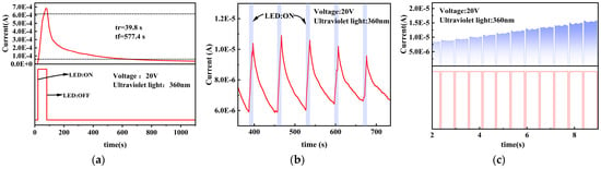
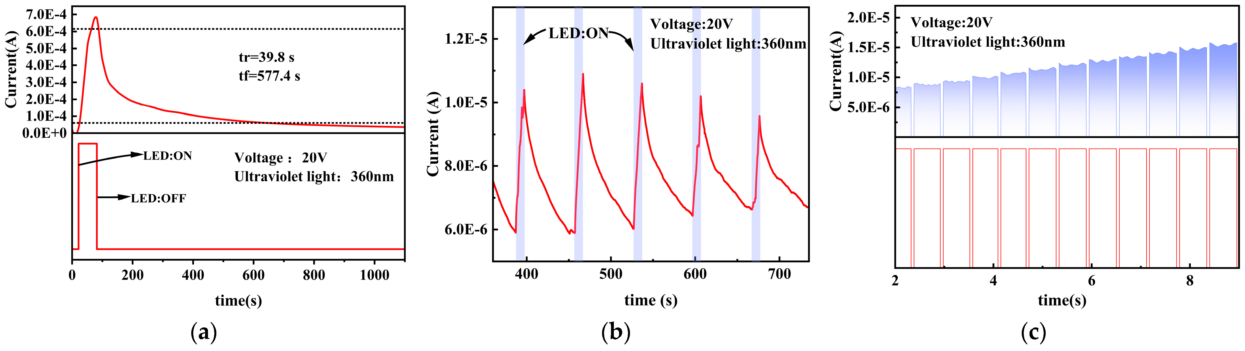
To evaluate the temporal response characteristics of the a-IGZO photodetector, Figure 8a presents the response curve under constant bias mode. The optimal device, featuring 60% indium content, was measured under 360 nm UV illumination at a bias of 20 V. The rise time (tr) and fall time (tf) are defined as the durations required for the photocurrent to increase from 10% to 90% and to decrease from 90% to 10% of its peak value, respectively. In constant bias mode, a bias of 20 V was maintained while the UV LED was pulsed with a single pulse width of 60 s. The device exhibits a rise time (tr) of approximately 39.8 s and a fall time (tf) of approximately 577.4 s. This prolonged recovery time is a typical manifestation of the intrinsic persistent photoconductivity (PPC) effect in IGZO materials [42], which arises from the trapping of photogenerated carriers by deep-level defects, such as oxygen vacancies, resulting in an extended electron lifetime. Previous studies have demonstrated that the concentration of oxygen vacancies is closely correlated with the PPC effect; a higher concentration leads to a more pronounced PPC effect [43].
Figure 8.
Temporal response of the a-IGZO MSM photodetector (60% In) under 360 nm UV illumination at 20 V bias. (a) Under constant bias mode, the device exhibits a tr of 39.8 s and a tf of 577.4 s; (b) time-dependent photoresponse under periodic UV illumination. (c) Current response under constant UV illumination with pulsed bias.
To further clarify the practical significance of pulsed bias operation, additional experiments were carried out. Figure 8b shows the photoresponse under periodic UV illumination. A constant bias of 20 V was applied, and the LED was switched on and off with durations of 10 s and 50 s, respectively, forming one cycle. The device exhibits stable and repeatable current switching behavior, indicating that it does not become inactive or “blind” even during prolonged operation. Although the decay process is relatively slow due to PPC, the device remains capable of responding effectively to subsequent illumination. To investigate the effect of pulsed bias, the current response was measured under constant UV illumination while periodically switching the bias between 0 V and 20 V, as shown in Figure 8c. A gradual increase in the baseline current is observed, which is attributed to persistent photoconductivity caused by trap-assisted carrier accumulation in IGZO. Superimposed on this trend, a clear periodic modulation of the current is observed, which corresponds to the applied bias. Specifically, the current increases when the bias is turned on and decreases when it is turned off, demonstrating a synchronized response between the electrical bias and carrier transport. Higher indium content introduces more oxygen vacancy-related trap states, leading to enhanced persistent photoconductivity and thus slower temporal response [44].
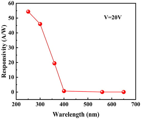
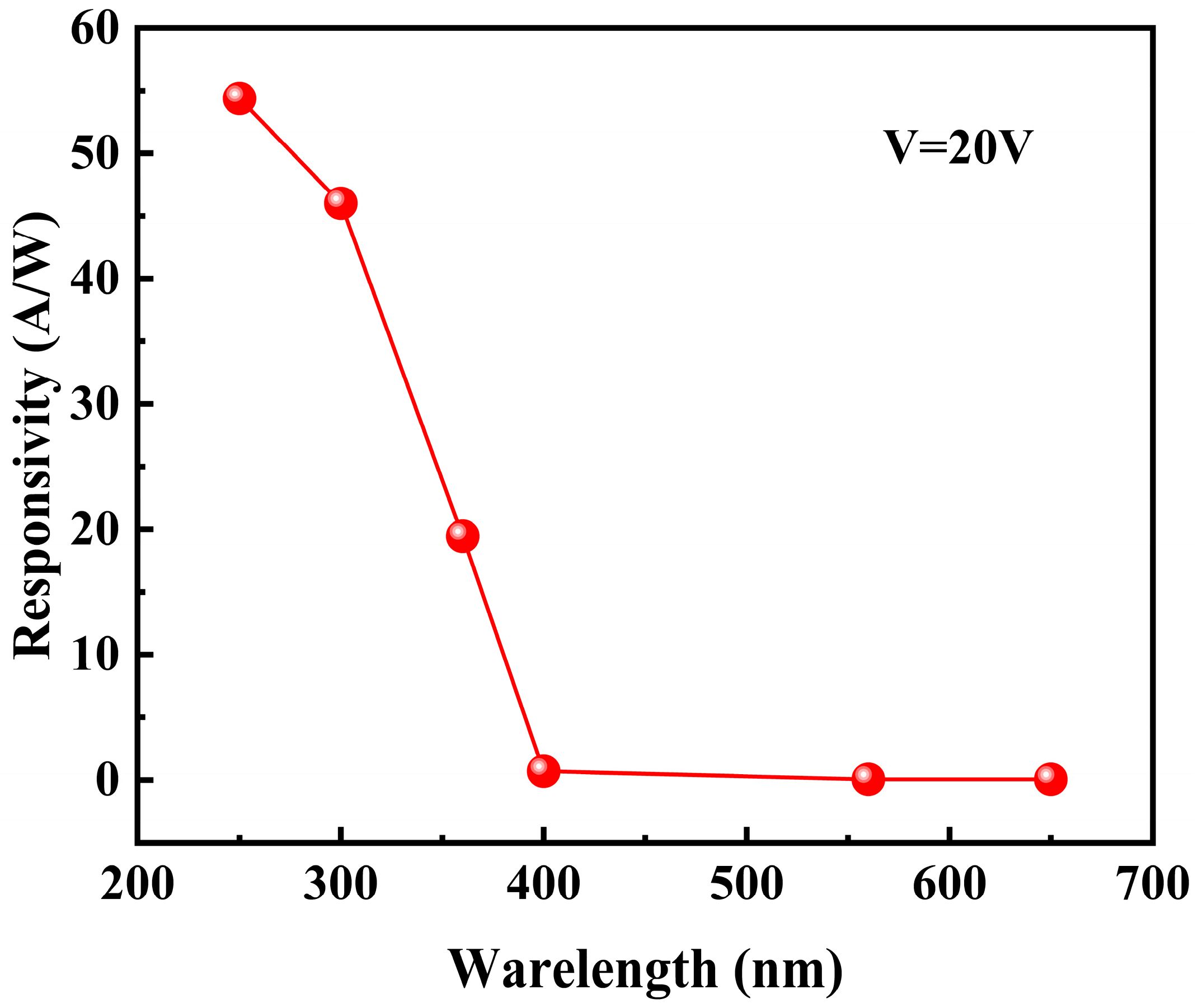
To evaluate the spectral selectivity of the A-IGZO MSM photodetector, we measured the broadband spectral responsivity of the optimal device, which has a 60% indium content, at a bias voltage of 20 V. LEDs with wavelengths of 250 nm, 310 nm, 360 nm, 400 nm, 560 nm, and 650 nm were used as light sources. The incident light power for each wavelength was recorded using a calibrated optical power meter, and the responsivity values were calculated accordingly. As shown in Figure 9, the device exhibits an R value of 19.45 A/W at a wavelength of 360 nm. The R values at wavelengths of 250 nm and 310 nm are 54.37 A/W and 46.00 A/W, respectively, both of which are higher than the responsivity at 360 nm. This phenomenon can be attributed to the higher photon energy at shorter wavelengths, which enhances absorption and improves quantum efficiency. The responsivity drops sharply to 0.71 A/W at 400 nm and further decreases to below 0.06 A/W at both 560 nm and 650 nm. The ultraviolet-visible light suppression ratio (R360 nm/R560 nm) is approximately 360, demonstrating excellent ultraviolet selectivity. This result confirms that the a-IGZO MSM photodetector prepared in this study is suitable for ultraviolet light detection and minimally affected by visible light.
Figure 9.
At a 20-volt voltage bias, the broadband spectral response rate of the 60% indium-based IGZO photodetector.
To further evaluate the performance of the devices, we compared the key parameters of the optimal device (60% In) presented in this study with those reported in the recent literature, summarizing the results in Table 2. The comparison highlights the inherent differences between magnetron sputtering and sol–gel methods: the sputtering technique yields dense, low-defect films characterized by lower dark current and faster response times, albeit with limited flexibility in component control. In contrast, the sol–gel method is more susceptible to defect introduction but offers excellent component tunability, making it suitable for systematic investigations of the structure-activity relationship in multi-component systems. This study effectively capitalizes on this characteristic, demonstrating that an increase in In concentration narrows the band gap and enhances light absorption. However, elevated In levels lead to a rise in oxygen vacancies, which introduce composite centers and amplify the photogenerated charge carrier PPC effect, resulting in a significant increase in the tf and a competition between enhanced light absorption and defect recombination losses.
Table 2.
Compares the key performance parameters of the optimal device (60% indium) adopted in this study with the corresponding parameters reported in previously published literature for ultraviolet light detectors based on a-IGZO. (Because the device architectures, illumination wavelengths, optical powers, and bias conditions vary across reports, this comparison is intended as a qualitative benchmark rather than a strict head-to-head ranking).
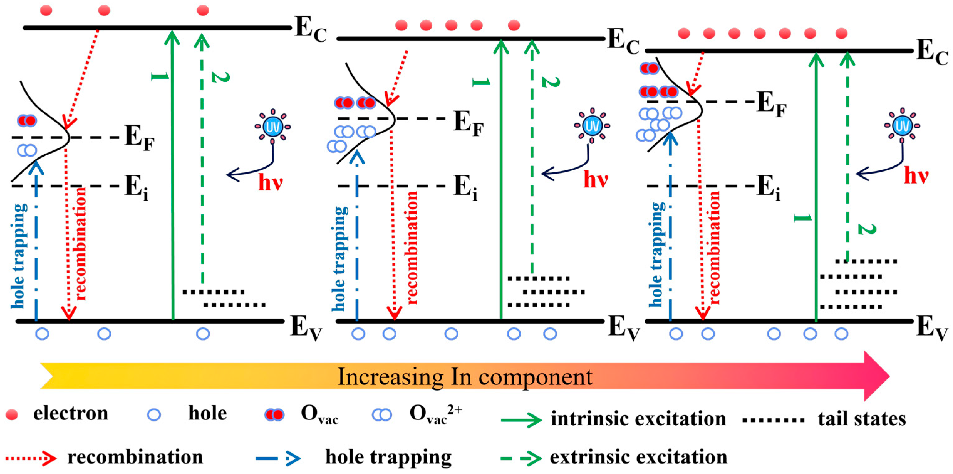
Figure 10 presents a schematic diagram of the energy band structure of different indium (In)-containing IGZO films under 360 nm ultraviolet light irradiation. By integrating the results of XPS, optical and electrical experiments, the influence of indium content on the generation, transport and recombination processes of charge carriers is systematically explained. Under dark conditions, as the indium content increases, it may lead to a decrease in the conduction band minimum (CBM), which corresponds to a reduction in the optical band gap and is consistent with the redshift trend observed in the Tauc analysis. Additionally, XPS results reveal that a higher In content introduces a greater number of oxygen-vacancy (Ovac)-related defect states, resulting in a denser distribution of band-tail states near the Fermi level. This phenomenon consequently enhances n-type conductivity and increases the dark current. Under ultraviolet (UV) illumination, the photogenerated nonequilibrium carriers primarily originate from two excitation pathways: (1) intrinsic band-to-band transitions from the valence band to the conduction band, and (2) sub-bandgap excitation from valence band tail states or oxygen-vacancy-related defect states to the conduction band [37]. For samples with lower In content, the defect-state density is relatively low, and intrinsic band-to-band excitation predominates, resulting in a lower recombination probability of photogenerated carriers. As the In content increases, the concentration of oxygen vacancies and their ionized states significantly rises, leading to a more extensive distribution of localized tail states within the bandgap. On one hand, these defect states facilitate sub-bandgap excitation and increase the concentration of photogenerated electrons, thereby enhancing the photocurrent. On the other hand, they also introduce additional recombination centers, which intensify carrier recombination and hole trapping, ultimately limiting further improvements in device performance. It will also lead to the PPC effect, causing the recovery time of 60% In component devices to be 577.4 s. Therefore, the variation in In composition exerts a dual effect on device performance: the downward shift in the energy band (bandgap narrowing) promotes carrier generation and transport, while the increase in defect-state density enhances the recombination probability and raises the dark current.
Figure 10.
Band diagrams of In-different component IGZO photodetectors.
4. Conclusions
In this study, a-IGZO MSM ultraviolet photodetectors with varying In compositions (ranging from 33% to 84%) were successfully fabricated using a sol–gel process. The modulation mechanism of In content on device performance was systematically elucidated. The experimental results demonstrate that as the In content increases from 33% to 84%, the films maintain a stable amorphous structure, while the oxygen vacancy ratio increases monotonically from 36% to 52%. Furthermore, the optical bandgap narrows from 2.92 eV to 2.32 eV, and the dark current rises significantly from 2.11 × 10⁻⁹ A to 1.90 × 10⁻⁵ A. The responsivity exhibits a non-monotonic behavior: it is only 3.22 × 10⁻³ A/W at 33% In, reaches a peak of 19.45 A/W at 60% In with a detectivity of 8.19 × 10¹² Jones, and subsequently decreases to 5.39 A/W and 2.82 A/W at 77% and 84% In, respectively. The physical origin of this trend can be attributed to the dual modulation mechanism of In composition on the electronic structure of IGZO. On one hand, the contribution of In 5s orbitals to the conduction band minimum increases with In content, leading to bandgap narrowing and enhanced ultraviolet absorption, which serves as the physical basis for the improved responsivity. On the other hand, the bond dissociation energy of In-O bonds is lower than that of Ga-O and Zn-O bonds; thus, higher In content is associated with a significant increase in the concentration of oxygen vacancies. These oxygen vacancies play a dual role: as shallow donors, they release free electrons and increase the background carrier concentration, resulting in an increased dark current; as deep-level traps, they introduce recombination centers and reduce the collection efficiency of photogenerated carriers. It is precisely this intrinsic competition between enhanced optical absorption and defect-related recombination loss that determines 60% In as the optimal composition that balances this trade-off. In terms of response speed, the device exhibits a typical PPC effect under constant bias, with a fall time as long as 577.4 s. This phenomenon is closely related to the relatively high concentration of oxygen vacancies in sol–gel-derived films. Notably, pulsed bias operation was employed in this study, which reduced the effective fall time to 20 microseconds, demonstrating that optimizing operational strategies can effectively overcome inherent material limitations. FTIR analysis reveals a very weak hydroxyl absorption band, confirming the effectiveness of the 400 °C annealing process under an O2 atmosphere. Furthermore, comparisons with existing literature support the intrinsic UV selectivity of a-IGZO materials. It should be noted that, compared with devices prepared through magnetron sputtering, the sol–gel-derived films contain a higher number of defects, resulting in a longer decay time. Additionally, the annealing temperature of 400 °C limits their direct application on flexible plastic substrates. Future improvements could be achieved by integrating low-temperature processes, such as photochemical activation or high-pressure annealing. The novelty of this work lies in the systematic revelation of the dual modulation mechanism of In composition on the performance of a-IGZO UV photodetectors, utilizing the compositional tunability of the sol–gel method. This mechanistic understanding provides a clear design principle for optimizing amorphous oxide UV photodetectors. The high-performance a-IGZO MSM UV photodetector successfully developed in this work. The results provide insight into the photoconduction mechanism and demonstrate the potential of sol–gel IGZO for UV detection.
Supplementary Materials
The following supporting information can be downloaded at: https://www.mdpi.com/article/10.3390/coatings16040494/s1, Figure S1: (a) FTIR spectrum of the sample in the range of 400–4600 cm−1. (b) Enlarged FTIR spectrum in the range of 1000–4600 cm−1, highlighting the spectral features in the higher wavenumber region, particularly the broad absorption band at 3200–3600 cm−1. Figure S2: Temporal photoresponse of IGZO photodetectors with different indium contents under UV illumination. Table S1: Extracted rise time and decay time of IGZO photodetectors with different indium contents under UV illumination. Figure S3: (a) In 3d spectrum; (b) Ga 2p spectrum; (c) Zn 2p spectrum. As the content of In increases, the peak intensity of In 3d becomes larger and larger, while the intensities of Ga 2p and Zn 2p become weaker and weaker. Refs. [1,28,48,49] are cited in the Supplementary Materials.
Author Contributions
Conceptualization, Z.Z. and X.L.; methodology, T.D.; software, Y.L.; validation, Y.H., Q.T. and L.Z.; formal analysis, J.P. and X.L.; investigation, J.L. (Ji Li); resources, X.W.; data curation, H.Q.; writing—original draft preparation, X.L.; writing—review and editing, M.H.; visualization, J.L. (Jiangping Luo); supervision, Z.Z.; project administration, S.L.; funding acquisition, Z.Z. and T.D. All authors have read and agreed to the published version of the manuscript.
Funding
This research was funded by the National Natural Science Foundation of China, grant number (No. 62264001), the Provincial Basic Research Program project of Guizhou, grant number (No. QKHJC-ZK[2022]YB009), the High Level Innovation Talents Project of Guizhou Province, grant number (No. ZKHT-GCC[2023]007), Research Project on Science and Technology of Guizhou Province, grant number (Qiankehe Foundation-ZK [2024] General No. 521) Research on Magnesium Boride Superconducting Integrated Circuit Technology, Guizhou Provincial Basic Research Program (Natural Science), grant number (No. QKHJC-ZK[2022]YB007), Guiyang University’s 2024 Undergraduate Innovation and Entrepreneurship Training Program Project (Research on the Preparation and Study of Special Carbon Materials Based on Waste from “Rich Ore Exploitation” in Guizhou), grant number (No. 2024109760063), Natural Science Research Project of Higher Education Institutions of Guizhou Provincial Education Department (Project for the Growth of Young Scientific Talents), grant number (Qianjiaoji [2024] No. 189) and Graduate Research Fund Project of Guiyang University [2024], grant number (No. 2024YJSKY02).
Institutional Review Board Statement
Not applicable.
Informed Consent Statement
Not applicable.
Data Availability Statement
The data presented in this study are available in this article. Further inquiries can be directed to the corresponding author.
Acknowledgments
The authors would like to thank Guiyang University for providing research facilities and technical support. The authors also appreciate the valuable suggestions from the anonymous reviewers and editors that helped improve the quality of this manuscript.
Conflicts of Interest
The authors declare no conflicts of interest. The funders had no role in the design of the study; in the collection, analyses, or interpretation of data; in the writing of the manuscript; or in the decision to publish the results.
References
- Nomura, K.; Ohta, H.; Takagi, A.; Kamiya, T.; Hirano, M.; Hosono, H. Room-temperature fabrication of transparent flexible thin-film transistors using amorphous oxide semiconductors. Nature 2004, 432, 488–492. [Google Scholar] [CrossRef] [Scilit]
- Cao, F.; Liu, Y.; Liu, M.; Han, Z.; Xu, X.; Fan, Q.; Sun, B. Wide bandgap semiconductors for ultraviolet photodetectors: Approaches, applications, and prospects. Research 2024, 7, 0385. [Google Scholar] [CrossRef] [Scilit]
- Liao, M.; Koide, Y. High-performance metal-semiconductor-metal deep-ultraviolet photodetectors based on homoepitaxial diamond thin film. Appl. Phys. Lett. 2006, 89, 113509. [Google Scholar] [CrossRef] [Scilit]
- Tan, J.; Yi, L.; Lv, M.; Zhang, M.; Bai, S. AlN Passivation-Enhanced Mg-Doped β-Ga2O3 MISIM Photodetectors for Highly Responsive Solar-Blind UV Detection. Coatings 2025, 15, 1312. [Google Scholar] [CrossRef] [Scilit]
- Zou, Y.; Zhang, Y.; Hu, Y.; Gu, H. Ultraviolet detectors based on wide bandgap semiconductor nanowire: A review. Sensors 2018, 18, 2072. [Google Scholar] [CrossRef] [Scilit]
- Lam, K.-T.; Young, S.-J.; Chu, Y.-L.; Tsai, C.-N.; Chu, T.-T.; Lu, T.-S.; Ji, L.-W. Characteristics of Metal–Semiconductor–Metal Ultraviolet Photodetectors Based on Pure ZnO/Amorphous IGZO Thin-Film Structures. J. Nanomater. 2021, 2021, 6649200. [Google Scholar] [CrossRef] [Scilit]
- Ganguly, S.; Kanovsky, N.; Das, P.; Gedanken, A.; Margel, S. Photopolymerized thin coating of polypyrrole/graphene nanofiber/iron oxide onto nonpolar plastic for flexible electromagnetic radiation shielding, strain sensing, and non-contact heating applications. Adv. Mater. Interfaces 2021, 8, 2101255. [Google Scholar] [CrossRef] [Scilit]
- Shin, S.W.; Lee, K.-H.; Park, J.-S.; Kang, S.J. Highly transparent, visible-light photodetector based on oxide semiconductors and quantum dots. ACS Appl. Mater. Interfaces 2015, 7, 19666–19671. [Google Scholar] [CrossRef] [Scilit]
- Murat, A.; Medvedeva, J.E. Composition-dependent oxygen vacancy formation in multicomponent wide-band-gap oxides. Phys. Rev. B—Condens. Matter Mater. Phys. 2012, 86, 085123. [Google Scholar] [CrossRef] [Scilit]
- Cho, S.; Kim, S.; Kim, D.; Yi, M.; Byun, J.; Song, P. Effects of yttrium doping on a-IGZO thin films for use as a channel layer in thin-film transistors. Coatings 2019, 9, 44. [Google Scholar] [CrossRef] [Scilit]
- Song, S.; Liang, H.; Huo, W.; Zhang, G.; Zhang, Y.; Wang, J.; Mei, Z. Low-voltage IGZO field-effect ultraviolet photodiode. Chin. Phys. Lett. 2024, 41, 068501. [Google Scholar] [CrossRef] [Scilit]
- Jang, J.T.; Ko, D.; Choi, S.; Kang, H.; Kim, J.-Y.; Yu, H.R.; Ahn, G.; Jung, H.; Rhee, J.; Lee, H.; et al. Effects of structure and oxygen flow rate on the photo-response of amorphous IGZO-based photodetector devices. Solid-State Electron. 2018, 140, 115–121. [Google Scholar] [CrossRef] [Scilit]
- Lin, C.-W.; Huang, K.-L.; Chang, K.-W.; Chen, J.-H.; Chen, K.-L.; Wu, C.-H. Ultraviolet photodetector and gas sensor based on amorphous In-Ga-Zn-O film. Thin Solid Films 2016, 618, 73–76. [Google Scholar] [CrossRef] [Scilit]
- Yu, J.; Javaid, K.; Liang, L.; Wu, W.; Liang, Y.; Song, A.; Zhang, H.; Shi, W.; Chang, T.-C.; Cao, H. High-performance visible-blind ultraviolet photodetector based on IGZO TFT coupled with p–n heterojunction. ACS Appl. Mater. Interfaces 2018, 10, 8102–8109. [Google Scholar] [CrossRef] [Scilit]
- Wang, M.; Zhang, J.; Xin, Q.; Yi, L.; Guo, Z.; Wang, Y.; Song, A. Self-powered UV photodetectors and imaging arrays based on NiO/IGZO heterojunctions fabricated at room temperature. Opt. Express 2022, 30, 27453–27461. [Google Scholar] [CrossRef] [Scilit]
- Kim, M.G.; Jeong, J.H.; Ma, J.H.; Park, M.H.; Kim, S.; Park, S.; Kang, S.J. A chemically treated IGZO-based highly visible-blind UV phototransistor with suppression of the persistent photoconductivity effect. J. Mater. Chem. C 2023, 11, 15178–15196. [Google Scholar] [CrossRef] [Scilit]
- Xiong, Z.; Kim, Y.J.; Park, M.; Chen, Y.-C.; Kim, M. Self-powered p-GaN/n-IGZO ultraviolet photodetectors with enhanced sensitivity enabled by antireflective nanopillars. Chem. Eng. J. 2025, 528, 172405. [Google Scholar] [CrossRef] [Scilit]
- Jiang, J.; Wu, S.; Ding, Z.; Xin, Q.; Tian, Y. High Responsivity Flexible β-Ga2O3/IGZO Ultraviolet Photodetectors Enabled by Zr-Modulated Quasi-Two-Dimensional Electron Gas Interfacial Confinement. ACS Photonics 2025, 12, 5884–5892. [Google Scholar] [CrossRef] [Scilit]
- Fortunato, E.; Barquinha, P.; Martins, R. Oxide semiconductor thin-film transistors: A review of recent advances. Adv. Mater. 2012, 24, 2945–2986. [Google Scholar] [CrossRef] [Scilit] [PubMed]
- Kim, G.H.; Du Ahn, B.; Shin, H.S.; Jeong, W.H.; Kim, H.J.; Kim, H.J. Effect of indium composition ratio on solution-processed nanocrystalline InGaZnO thin film transistors. Appl. Phys. Lett. 2009, 94, 233501. [Google Scholar] [CrossRef] [Scilit]
- Cadis, A.I.; Muresan, L.E.; Perhaita, I.; Barbu-Tudoran, L.; Borodi, G. Copper indium sulphide nanoparticles with tunable energy band gap obtained by ultrasound-assisted precipitation. J. Optoelectron. Adv. Mater. 2020, 22, 613–618. [Google Scholar]
- Hosono, H. Ionic amorphous oxide semiconductors: Material design, carrier transport, and device application. J. Non-Cryst. Solids 2006, 352, 851–858. [Google Scholar] [CrossRef] [Scilit]
- Jeong, S.; Ha, Y.; Moon, J.; Facchetti, A.; Marks, T.J. Role of gallium doping in dramatically lowering amorphous-oxide processing temperatures for solution-derived indium zinc oxide thin-film transistors. Adv. Mater. 2010, 22, 1346–1350. [Google Scholar] [CrossRef] [Scilit]
- Abdullah; Hosain, M.; Parvez, M.H.; Motayed, S.H. Prospects and challenges of thin film coating materials and their applications. Inorg. Chem. Commun. 2025, 175, 114117. [Google Scholar] [CrossRef] [Scilit]
- Hsu, C.-M.; Tzou, W.-C.; Yang, C.-F.; Liou, Y.-J. Investigation of the high mobility IGZO thin films by using co-sputtering method. Materials 2015, 8, 2769–2781. [Google Scholar] [CrossRef] [Scilit]
- Yao, J.; Zhang, S.; Gong, L. Band offsets in ZrO2/InGaZnO4 heterojunction. Appl. Phys. Lett. 2012, 101, 093508. [Google Scholar] [CrossRef] [Scilit]
- Seo, S.J.; Hwang, Y.H.; Bae, B.S. Postannealing process for low temperature processed sol–gel zinc tin oxide thin film transistors. Electrochem. Solid-State Lett. 2010, 13, H357–H359. [Google Scholar] [CrossRef] [Scilit]
- Kamiya, T.; Nomura, K.; Hosono, H. Present status of amorphous In–Ga–Zn–O thin-film transistors. Sci. Technol. Adv. Mater. 2010, 11, 044305. [Google Scholar] [CrossRef] [Scilit] [PubMed]
- Tsay, C.Y.; Yan, T.Y. Solution processed amorphous InGaZnO semiconductor thin films and transistors. J. Phys. Chem. Solids 2014, 75, 142–147. [Google Scholar] [CrossRef] [Scilit]
- Sasajima, H.; Morimoto, T.; Fukuda, N.; Ishii, K. Effect of ozone gas exposure on drain current of solution-processed IGZO-TFT. Appl. Phys. A 2024, 130, 826. [Google Scholar] [CrossRef] [Scilit]
- Kim, E.; Jang, W.J.; Kim, W.; Park, J.; Lee, M.K.; Park, S.-H.K.; Choi, K.C. Suppressed instability of a-IGZO thin-film transistors under negative bias illumination stress using the distributed Bragg reflectors. IEEE Trans. Electron Devices 2016, 63, 1066–1071. [Google Scholar] [CrossRef] [Scilit]
- Yoshidomi, S.; Kimura, S.; Hasumi, M.; Sameshima, T. Indium–gallium–zinc–oxide layer used to increase light transmittance efficiency of adhesive layer for stacked-type multijunction solar cells. Jpn. J. Appl. Phys. 2015, 54, 112301. [Google Scholar] [CrossRef] [Scilit]
- Chen, M.-C.; Chang, T.-C.; Huang, S.-Y.; Chen, S.-C.; Hu, C.-W.; Tsai, C.-T.; Sze, S.M. Bipolar resistive switching characteristics of transparent indium gallium zinc oxide resistive random access memory. Electrochem. Solid-State Lett. 2010, 13, H191–H193. [Google Scholar] [CrossRef] [Scilit]
- Leenheer, A.J.; Perkins, J.D.; van Hest, M.F.A.M.; Berry, J.J.; O’hayre, R.P.; Ginley, D.S. General mobility and carrier concentration relationship in transparent amorphous indium zinc oxide films. Phys. Rev. B-Condens. Matter Mater. Phys. 2008, 77, 115215. [Google Scholar] [CrossRef] [Scilit]
- Xue, S.; Zu, X.; Zhou, W.; Deng, H.; Xiang, X.; Zhang, L.; Deng, H. Effects of post-thermal annealing on the optical constants of ZnO thin film. J. Alloys Compd. 2008, 448, 21–26. [Google Scholar] [CrossRef] [Scilit]
- Li, T.; Grudowski, P.A.; Eiting, C.J.; Dupuis, R.D.; Campbell, J.C. Comprehensive characterization of metal–semiconductor–metal ultraviolet photodetectors fabricated on single-crystal GaN. J. Appl. Phys. 1998, 83, 6148–6160. [Google Scholar]
- Zhang, Y.Y.; Qian, L.X.; Wu, Z.H.; Lai, P.T.; Liu, X.Z. Improved performance of amorphous ingamgo metal-semiconductor-metal ultraviolet photodetector by post deposition annealing in oxygen. IEEE Trans. Nanotechnol. 2016, 17, 29–35. [Google Scholar] [CrossRef] [Scilit]
- Hamilton, M.C.; Martin, S.; Kanicki, J. Thin-film organic polymer phototransistors. IEEE Trans. Electron Devices 2004, 51, 877–885. [Google Scholar] [CrossRef] [Scilit]
- Li, X.; Zhu, M.; Du, M.; Lv, Z.; Zhang, L.; Li, Y.; Yang, Y.; Yang, T.; Li, X.; Wang, K.; et al. High detectivity graphene-silicon heterojunction photodetector. Small 2016, 12, 595–601. [Google Scholar] [CrossRef] [Scilit]
- Rogalski, A. Infrared detectors: Status and trends. Prog. Quantum Electron. 2003, 27, 59–210. [Google Scholar] [CrossRef] [Scilit]
- Kim, C.-J.; Lee, H.-S.; Cho, Y.-J.; Kang, K.; Jo, M.-H. Diameter-dependent internal gain in ohmic Ge nanowire photodetectors. Nano Lett. 2010, 10, 2043–2048. [Google Scholar] [CrossRef] [Scilit] [PubMed]
- Li, Y.; Zhao, Y.; Zhu, X. Effect of Interdigitated Electrode Spacing on the Performance of Flexible InGaZnO Ultraviolet Photodetectors. J. Wuhan Univ. Technol.-Mater. Sci. Ed. 2025, 40, 307–315. [Google Scholar] [CrossRef] [Scilit]
- Moon, S.J.; Kim, J.Y.; Kim, J.; Bae, B.S. Photo response of a-IGZO thin films as a function of annealing temperature. J. Inf. Disp. 2025, 26, 461–471. [Google Scholar] [CrossRef] [Scilit]
- Yao, J.; Liu, S.; Liu, X. Amorphous IGZO MIS phototransistor with HfO2 gate dielectrics for high sensitivity solar-blind ultraviolet detection. IEEE Trans. Electron Devices 2024, 71, 6743–6748. [Google Scholar] [CrossRef] [Scilit]
- Schellander, Y.; Winter, M.; Schamber, M.; Munkes, F.; Schalberger, P.; Kuebler, H.; Pfau, T.; Fruehauf, N. Ultraviolet photodetectors and readout based on a-IGZO semiconductor technology. J. Soc. Inf. Disp. 2023, 31, 363–372. [Google Scholar] [CrossRef] [Scilit]
- Liao, T.I.; Chang, S.P. Fast-response Indium Aluminum Gallium Oxide UV Photodetectors with Improved Responsivity. Int. J. Electrochem. Sci. 2025, 20, 101146. [Google Scholar] [CrossRef] [Scilit]
- Diao, Z.; Gong, T.; Li, X.; Hu, Y.; Hu, W. Solution-processed perovskite and oxide-semiconductor heterostructure construction for a high-performance ultraviolet photodetector. ACS Appl. Electron. Mater. 2024, 6, 2316–2322. [Google Scholar] [CrossRef] [Scilit]
- Hüfner, S. Photoelectron Spectroscopy: Principles and Applications; Springer Science & Business Media: Berlin/Heidelberg, Germany, 2013. [Google Scholar]
- Jeong, J.K.; Jeong, J.H.; Yang, H.W.; Park, J.S.; Mo, Y.G.; Kim, H.D. High performance thin film transistors with cosputtered amorphous indium gallium zinc oxide channel. Appl. Phys. Lett. 2007, 91, 113505. [Google Scholar] [CrossRef] [Scilit]

Disclaimer/Publisher’s Note: The statements, opinions and data contained in all publications are solely those of the individual author(s) and contributor(s) and not of MDPI and/or the editor(s). MDPI and/or the editor(s) disclaim responsibility for any injury to people or property resulting from any ideas, methods, instructions or products referred to in the content. |
© 2026 by the authors. Licensee MDPI, Basel, Switzerland. This article is an open access article distributed under the terms and conditions of the Creative Commons Attribution (CC BY) license.