


Abstract
Molecular dynamics simulations were used to study the interaction of Ar clusters with silicon and germanium single crystals at a fixed cluster size of 923 atoms and a total kinetic energy of 10 keV. A comparative analysis was conducted to examine the effects of argon cluster impacts on the surface morphology of silicon and germanium as the cluster incidence angle varied from 0° to 75° with respect to the surface normal. The depth of amorphization and the height of hillocks induced in silicon and germanium after argon cluster bombardment were estimated. Angular dependences of the crater diameters along and perpendicular to the cluster incidence direction were demonstrated. Comparisons of crater characteristics and the ratios of longitudinal to transverse crater dimensions revealed material-specific features of cluster–surface interactions. At oblique incidence, a peak in the ratio of displaced atoms in the amorphous layer to those above the surface was observed. The potential energy of silicon and germanium target atoms following cluster impact was visualized and estimated. Moreover, the redistribution patterns of the cluster’s initial kinetic energy among the target, scattered cluster atoms, and sputtered target atoms were compared for silicon and germanium at incidence angles from 0° to 75°.
1. Introduction
Gas cluster ion beams (GCIB) have emerged as a powerful tool for surface modification and analysis due to their unique interaction dynamics at the nanoscale. In contrast to monomer ion impacts, which involve high-energy individual atoms, cluster ion impacts entail the simultaneous collision of thousands of low-energy atoms with a similar volume of the target, producing dense, nonlinear energy deposition [1,2,3,4,5,6,7,8]. These interactions are characterized by energies per cluster atom in the range of a few to several tens of electron–volts—comparable to the binding energy of target atoms [7,9]—thereby enabling low-damage sputtering, atomic-level smoothing, and controlled surface nanostructuring [1,2,3,4,5,6].
The forcefulness of GCIB in applications such as surface smoothing [1,2,3,4,5,6], ion etching [1,2,3,4,5], self-organized nanostructuring [1,2,3,4,5], and surface-sensitive analytical techniques (e.g., SIMS and XPS) [8,10,11,12,13,14,15] stems from its ability to produce atomically flat surfaces at normal incidence [1,2,3,4,5,6], induce anisotropic nanostructuring at oblique incidence [1,2,3,4,5], and sputter intact molecular species from organic materials [8,9,10,11,12,13,14,15].
Most existing molecular dynamics (MD) simulations focus on argon clusters bombarding single-component materials such as Si [16,17,18,19,20,21], metals [6,21,22,23,24,25,26], or polymers [9,10]. The interaction dynamics depend critically on the target material properties, cluster size N, cluster energy E, mass of the cluster atoms, and incidence angle. MD simulations have proven invaluable for investigating GCIB-induced surface phenomena, including sputtering [10,23,24,25,26,27,28,29], atomic displacement [16,17,26,27,28], and crater and nanostructure formation [9,18,19,20,21,22,23,27,28,29,30]. In contrast to monomer impacts, clusters generate craters with complex morphologies and nonlinear scaling of sputtering yield and volume. Studies have shown that the diameter of craters formed by 60 keV Ar12 clusters can reach several nanometers, with lateral displacement of target atoms extending up to 50 nm [19]. Aoki T. et al. investigated the angular dependence of crater formation under 20 keV Ar2000 cluster irradiation of silicon and showed that crater characteristics and a number of displacements exhibits nonlinear scaling with total cluster energy and cluster size [17,18]. Nazarov A.V. et al. investigated the characteristics of lateral sputtering of target atoms and demonstrated that the thermal spike mechanism with small emission angles dominates at high energy per atom E/N. In contrast, at low E/N values, atoms located at the crater rim acquire significant lateral momentum, resulting in the formation of pronounced “lateral” angular distributions of sputtered atoms [23]. A recent study by Yu F. et al. examined the impact of 50 keV Ar3000 cluster on a Ge surface under oblique bombardment. The angular dependences of the crater depth as well as the height and width of the protrusion on the angle of incidence were analyzed. The results indicated that the directional protrusion effect is primarily governed by atom migration at large incidence angles [27]. Our recent MD results highlight that the ratio of crater length to depth is a function of the energy per cluster atom E/N. Even for clusters of different gas species, such as Ne and Kr, the depths of impact craters differ only slightly at oblique incidence. In addition, the cratering efficiency of different gas species was evaluated, and a relationship between crater volume and sputtering yield was established [30].
A deeper understanding of sputtering, cratering, and surface nanopatterning processes is essential for optimizing GCIB-based surface engineering and semiconductor processing technologies. Clarifying the roles of cluster size, energy, and incidence angle will improve theoretical models, broaden practical applications, and further enhance the controllability and precision of GCIB-based methods.
Despite extensive experimental and computational efforts, the fundamental mechanisms governing cluster–solid interactions, including energy dissipation, crater evolution, and angular effects, remain incompletely understood and require further clarification. Previous studies have typically considered Si and Ge separately, employing significantly different cluster parameters. In this work, we present a comparative molecular dynamics study of Ar cluster impact on Si and Ge surfaces over a wide range of incidence angles under identical conditions, thereby addressing an evident gap in the existing literature. The primary focus is on changes in the target surface morphology induced by cluster impact. The processes under investigation are governed by the transfer of kinetic energy from incident clusters to the target. Therefore, for the first time, particular attention is given to the redistribution of cluster kinetic energy among its key channels, including the energy transferred to the target, the energy of scattered cluster atoms, and the energy of sputtered target atoms.
2. MD Simulation Details
The impacts of individual argon clusters on single-crystal silicon and germanium have been simulated and examined. MD simulation of gas cluster ion impacts was performed using the LAMMPS computer code (https://github.com/lammps/lammps/releases accessed on 23 July 2025) [31]. The target slabs were Si and Ge crystals of 40 × 40 × 30-unit cells, corresponding to 384’000 target atoms and dimensions of 217 × 217 × 163 Å for Si and 226 × 226 × 170 Å for Ge. The initial targets densities were 2.33 and 5.32 g/cm3, corresponding to the densities of pure single-crystal Si and Ge, respectively. A fixed layer consisting of two sublayers—a frozen and a thermostated one—was created at the walls and bottom of the target. The thickness of the frozen sublayer was one unit cell. The thickness of the second sublayer was equal to two monolayers of thermostatic atoms, with zero target temperature. The Lennard-Jones potential was used to describe interactions between Ar atoms [32,33,34]. The Si–Si and Ge–Ge interactions were described using the Tersoff potential [35]. All close range interactions including between cluster and target atoms were described using the Ziegler–Biersack–Littmark (ZBL) potential [36].
The Atomic Simulation Environment (ASE) was used to create both projectile Ar gas clusters and target slabs [37]. Argon clusters were modeled using a Mackay icosahedral structure with a “magic number” of 923 atoms, which is close to the commonly used cluster size of N = 1000 atoms/cluster. The total kinetic energy of each cluster was set to 10 keV. Hence, the energy per atom E/N was about 10 eV/atom, corresponding to the low-energy processing regime used in the technological surface treatment of materials [1,2,3,4,5,6,38,39]. The principal incidence angles of Ar clusters were 0°, 15°, 30°, 45°, 60°, and 75°. Experimental data suggest that the optimal cluster incidence angles for effective nanostructure formation on various material surfaces are in the range of 55–65° [2,40,41,42,43]. Based on these results, additional simulations of cluster impacts on silicon and germanium surfaces were performed at incidence angles of 50°, 55°, 65°, and 70°.
Cluster impacts were simulated using the MD method within the mixed ensemble: number of atoms N and system volume V were constant, the temperature at the thermostated layer near the walls was fixed at T = 0 via global velocity rescaling method, and dynamics of other atoms, excluding fixed walls, was driven by time integration within microcanonical ensemble as enabled by the “fix nve” command in LAMMPS [31]. This ensemble has allowed us to simulate energy dissipation in the target and dynamics at the impact point. The total simulated time was 55 ps, with a time step of 0.1 fs for the initial 5 ps and 1 fs for the remaining 50 ps. All simulations were repeated five times for each parameter set. For repeated simulations with normal incidence, the initial cluster position was shifted by 5 Å along the Ox axis. For repeated oblique impacts, the azimuthal angles of incidence have been varied: 0°, 30°, 45°, 60°, and 90°. Visualization of surface morphology and atomic energy was performed using OVITO software 2.8.2 [44].
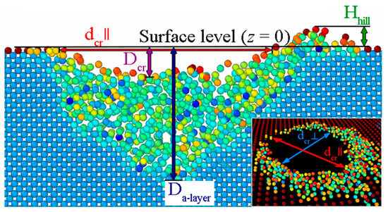
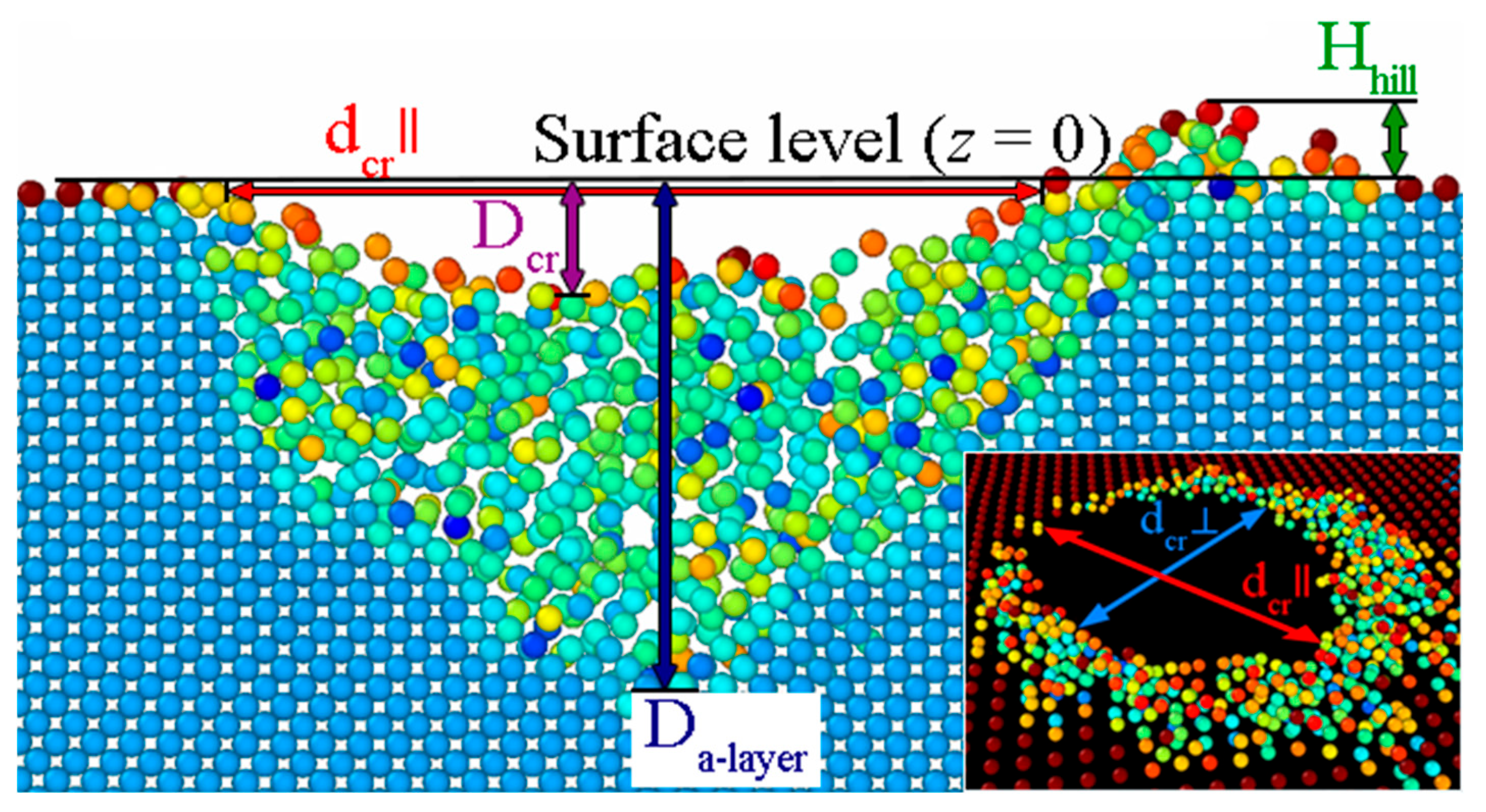
To characterize the effects of argon cluster impact on Si and Ge surfaces, the morphology of impact craters, the number of atomic displacements, and the redistribution of the initial cluster kinetic energy were analyzed. The crater morphology includes the overall shape, the depth of the amorphous layer, and the geometric dimensions, including the crater depth and the longitudinal and transverse diameters. The longitudinal and transverse crater diameters were defined as the lateral dimensions of the void region (i.e., the absence of atoms) at the surface level (z = 0). The definitions of the crater characteristics are illustrated in Figure 1.
Figure 1.
Schematic illustration of the crater, amorphous layer, and hillock parameters used in this study. The color of atoms corresponds to the potential energy of atoms, ranging from −4.6 eV (blue) to −2 eV (red).
The number of displacements was determined using the algorithm proposed by Maras et al. and implemented in OVITO software [44]. This algorithm is conceptually similar to the Common Neighbors Analysis algorithm but adapted for diamond cubic lattices. Atoms not identified by the algorithm as belonging to the diamond cubic structure were classified as “displaced”, and the corresponding volume was defined as “amorphous region”. The potential energy of target atoms was evaluated using the OVITO software.
The energy of scattered cluster atoms Escatt was calculated as the sum of the kinetic energies of all argon atoms after scattering from the target. Similarly, the energy of sputtered target atoms Esputt was obtained as the sum of the kinetic energies of all ejected atoms. The energy transferred to the target Etarget was then estimated as the difference between the initial kinetic energy of the cluster E0 and the energies of scattered (Escatt) and sputtered (Esputt) atoms. This transferred energy is dissipated through redistribution within the target and the ejection of target atoms, as well as through shock wave formation in the target volume, elastic lattice vibrations, and other dissipative processes.
3. Results and Discussion
3.1. Surface Morphology Evolution by Cluster Impacts
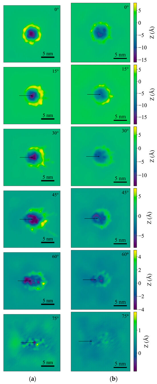
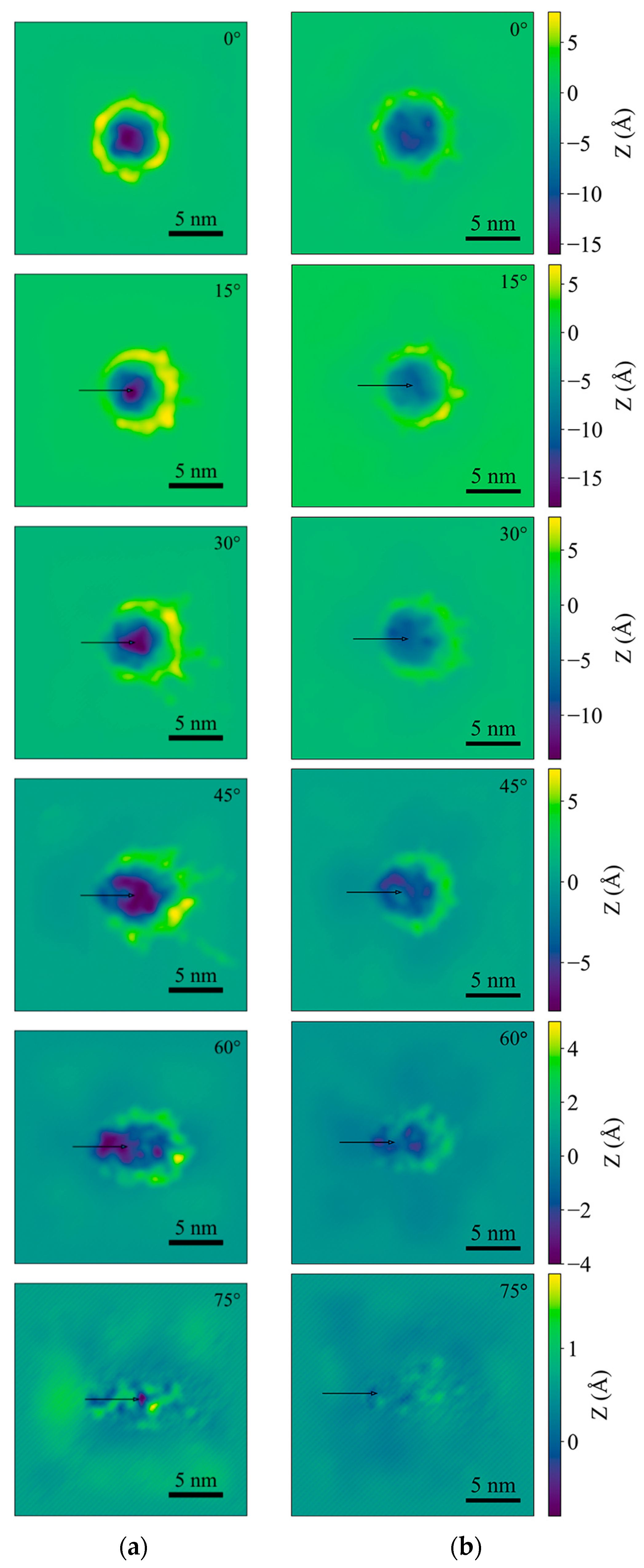
Top-view and cross-sectional snapshots of silicon and germanium after impact of a 10 keV Ar923 cluster at incidence angles ranging from 0° to 75° and an azimuthal angle of 0° are shown in Figure 2 and Figure 3, respectively. Figure 2 presents the surface morphology of Si and Ge as the cluster incidence angle increases at 55 ps. The surface atoms in Figure 2 are rendered as a solid surface for improved visual clarity. The images clearly illustrate differences in crater and hillock morphology between the Si and Ge targets. Notably, the crater diameter on Si is smaller than that on Ge at incidence angles up to 30°. This is most likely because more atoms are displaced above the Si surface, resulting in a higher and wider hillock and a deeper, narrower crater in Si. As the cluster incidence angle increases, the hillock height decreases from 0.9 nm for Si and from 0.6 nm for Ge until it disappears. The maximum hillock width reaches 2.3 nm at oblique incidence.
Figure 2.
Snapshots of the crater formation induced by 10 keV Ar923 clusters on Si (a) and Ge (b) surfaces at normal and oblique incidences after 55 ps. The colormap is normalized to maintain the same z-scale for the Si and Ge images at each impact angle. The colormap ranges from the deepest crater floor to the maximum hillock height. The cluster ion direction is indicated by a black arrow.
Figure 3.
Cross-sectional snapshots of 10 keV Ar923 bombardment of Si (a) and Ge (b) surfaces at normal and oblique incidences after 55 ps. The cluster ion direction is indicated by a black arrow. The colormap corresponds to the potential energy of target atoms, ranging from −4.6 eV (blue) to −2 eV (red).
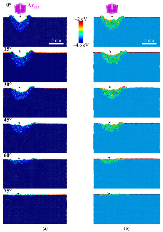
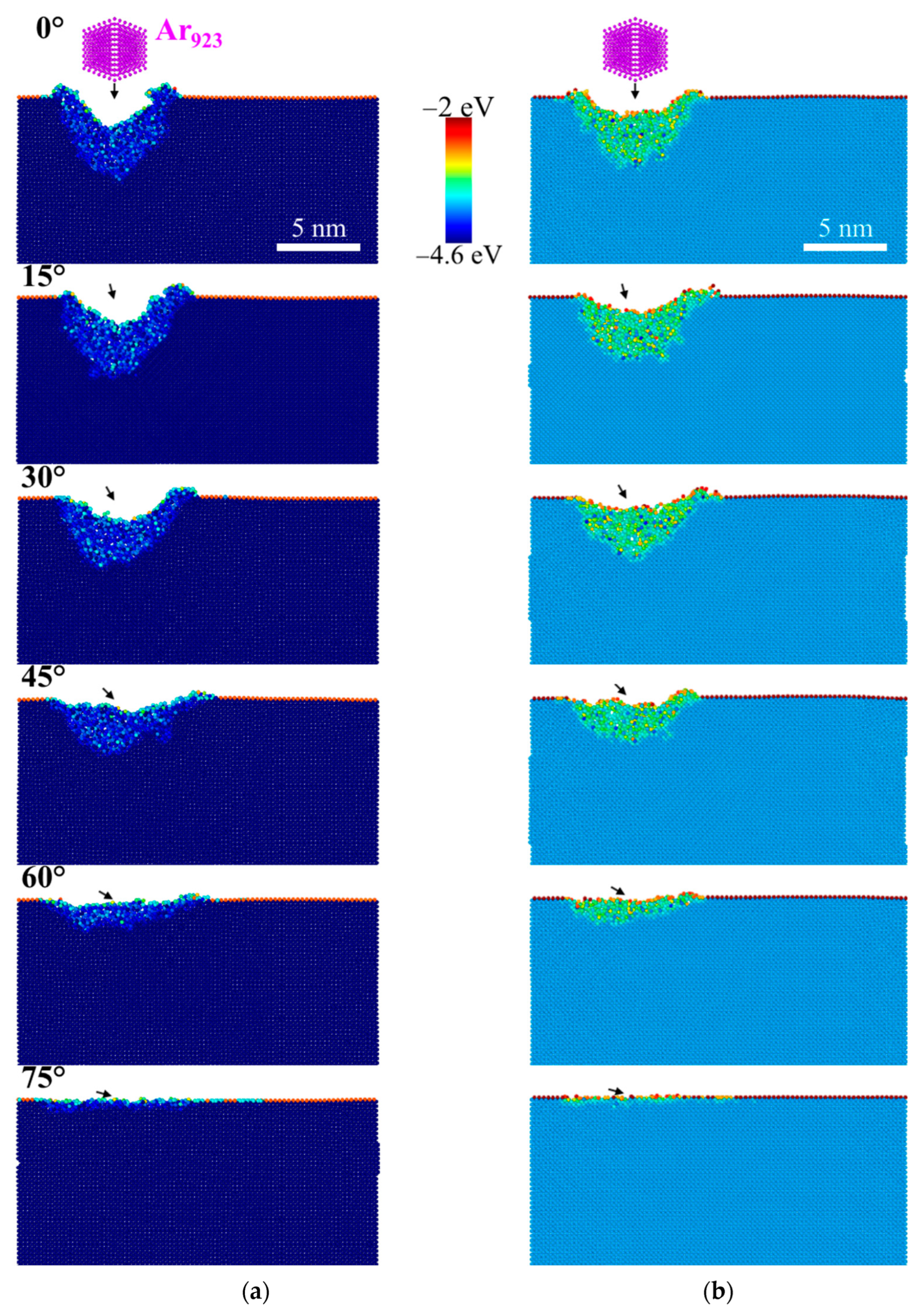
Figure 3 illustrates cross-sectional snapshots of silicon and germanium after impact of 10 keV Ar923 cluster. The cross-sectional thickness is 1 nm. The coloring of target atoms in Figure 3 corresponds to the potential energy Ep of the atoms. Foremost, this clearly highlights the distinction between the amorphous and crystalline regions formed after impact. The molar mass of silicon is approximately 2.6 times lower than that of germanium, which likely contributes to formation of sharper pits and bottom of the amorphized region in silicon. In addition, a pronounced difference in Ep values between Si and Ge is evident. A detailed analysis of potential energy is provided in the Section 3.2. As can be seen in Figure 2 and Figure 3, only minor surface disturbances with shallow depressions appear at an incidence angle of 75°, while the amorphous layer thickness is limited to a few monolayers.
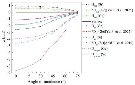
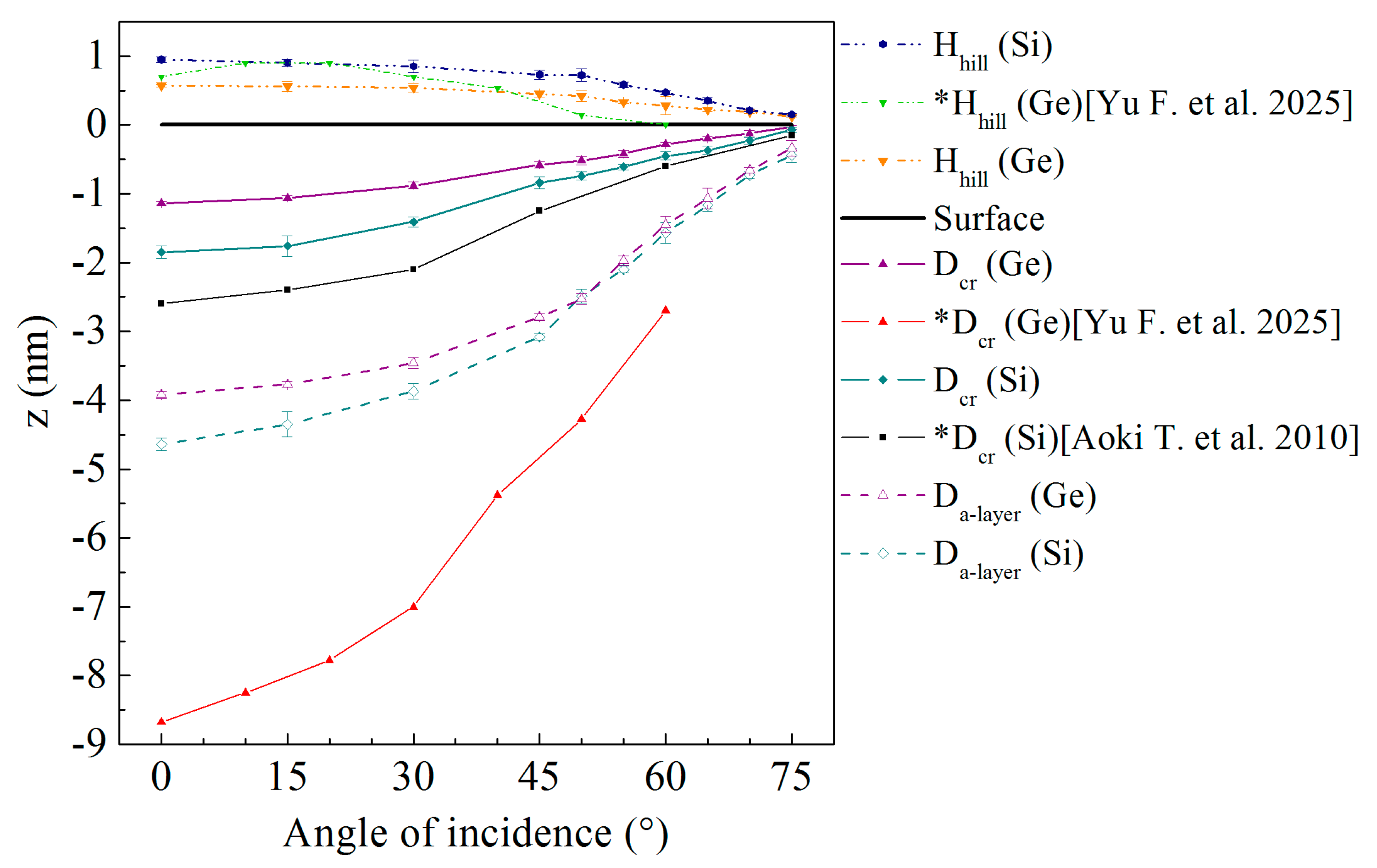
Figure 4 presents the quantitative characteristics of the impact crater, including the hillock height Hhill, the amorphous layer depth Da-layer, and the crater depth Dcr as functions of incidence angle. For clarity, these parameters are plotted relative to the surface level (z = 0). As can be seen in Figure 4, the depth of amorphization Da-layer decreases more rapidly at angle exceeding 45°. Up to 50°, silicon exhibits the amorphized depth 10%–18% greater (depending on incidence angle) than that of germanium. However, both materials show nearly identical amorphized depths beyond this angle. As mentioned above, previous studies indicate that optimal angles of cluster incidence for effective nanostructure formation lie in within 55–65°. Notably, our earlier experimental work [41] demonstrated that oblique irradiation of Si and Ge surfaces under identical conditions produces ripples with comparable structural parameters. As reported in Ref. [45], mass rearrangement at the amorphous–crystal interface contributes to the emergence of ripples under oblique incidence. Thus, similar amorphization depths in different materials may be one of the reasons for the formation of ripples with comparable structural parameters.
Figure 4.
Angular dependences of hillock height and amorphized and crater depths after Ar923 cluster impact on Si and Ge targets. “*” indicates adjusted data relative to the local surface normal for consistent comparison [18,27].
In contrast to the amorphized depth, the difference in crater depth Dcr between Si and Ge persists across the entire angular range, remaining 1.4–2 times greater for silicon. For comparison, values of Dcr reported by Aoki T. et al. [18] for Si and Yu F. et al. [27] for Ge are also plotted in Figure 4. Aoki T. et al. investigated impacts of 20 keV Ar2000 clusters on silicon at various angles and showed that the crater depth Dcr depends nonlinearly on both cluster energy E and size N. For example, increasing cluster energy E from 20 keV to 100 keV enlarges the crater depth Dcr from 2.3 nm to 4.7 nm, whereas reducing cluster size from 2000 atoms to 400 atoms at 20 keV raises Dcr only from 2.3 nm to 2.8 nm [18]. In both cases, the energy per atom E/N lies within the same range of 10–50 eV/atom, indicating that variations in total cluster energy E exert a stronger influence on crater depth Dcr than changes in cluster size N. Consequently, although the energy per atom in our study and in Ref. [18] is nearly identical (E/N ≈ 10 eV/atom), the crater depth Dcr in our simulations is about 1.5 times smaller, reflecting the dominant role of total cluster energy.
Yu F. et al. [27] examined impact of 50 keV Ar3000 clusters (E/N ≈ 16.7 eV/atom) on a germanium target at different incidence angles. In that work [27], a sinusoidal peak structure was introduced on a flat substrate to mimic realistic surface roughness. The angle between the z-axis and the local normal to the impact surface (center of the peak sidewall) was approximately 20°, so their data in Figure 4 were corrected to incidence angles measured from the local surface normal for consistent comparison. Overall, our crater-depth trend agrees well with that of Yu F. et al. for angles from 0° to 60°: the crater depth Dcr decreases by 4 times in our simulations and by 3.2 in theirs. At the same time, the maximum hillock height Hhill occurs at the normal incidence in our case, whereas in Ref. [27] it appears near 20°. The discrepancies in the absolute values of both the crater depths Dcr and hillock height Hhill for Ge can be attributable to differences in cluster parameters and to sidewall bombardment conditions employed in Ref. [27].
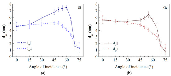
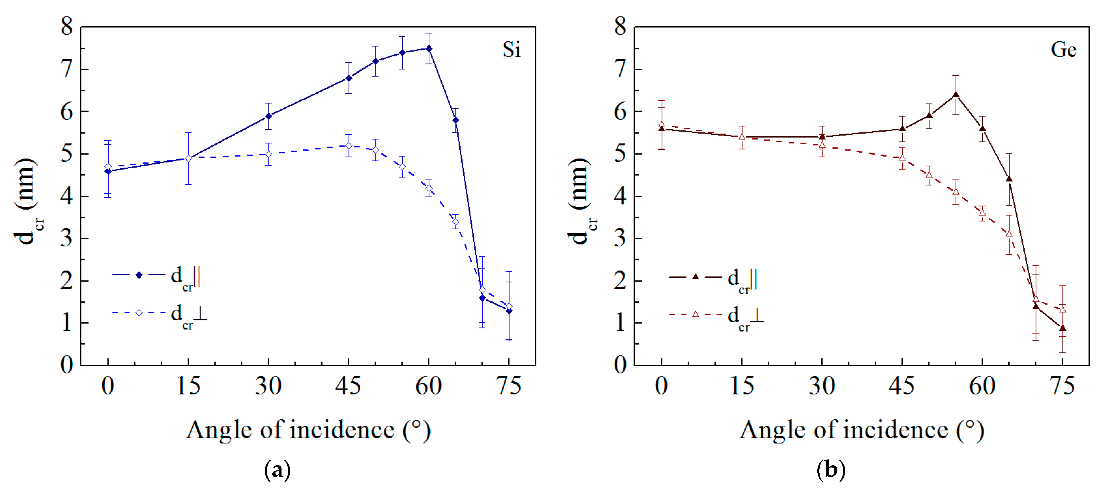
Figure 5 presents the angular dependences of crater diameters after Ar923 cluster impact on Si and Ge. The longitudinal and transverse crater diameters—corresponding to the major and minor axes of the elliptical crater formed at oblique incidence—are denoted as “dcr∥” and “dcr⟂”, respectively, reflecting their orientation parallel and perpendicular to the cluster incidence direction. Comparing diameter trends between the two similar semiconductor materials is of particular interest. As can be seen from Figure 5, both materials exhibit a pronounced peak in the longitudinal diameter of the impact crater dcr∥ within the incident angle range of 50–65°. Furthermore, the diameters of impact craters on Si exceed those on Ge by approximately 15%–20% at angles of incidence above 30°. The maximum dcr∥ reaches 7.5 nm at 60° for Si and 6.5 nm at 55° for Ge. At incident angles of 70° and 75°, impact craters are no longer observed, so the diameters of the largest pits within the disturbed surface region are presented instead.
Figure 5.
Angular dependences of crater diameters after Ar923 cluster impact on Si (a) and Ge (b) targets.
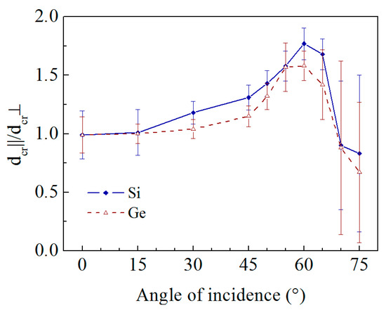
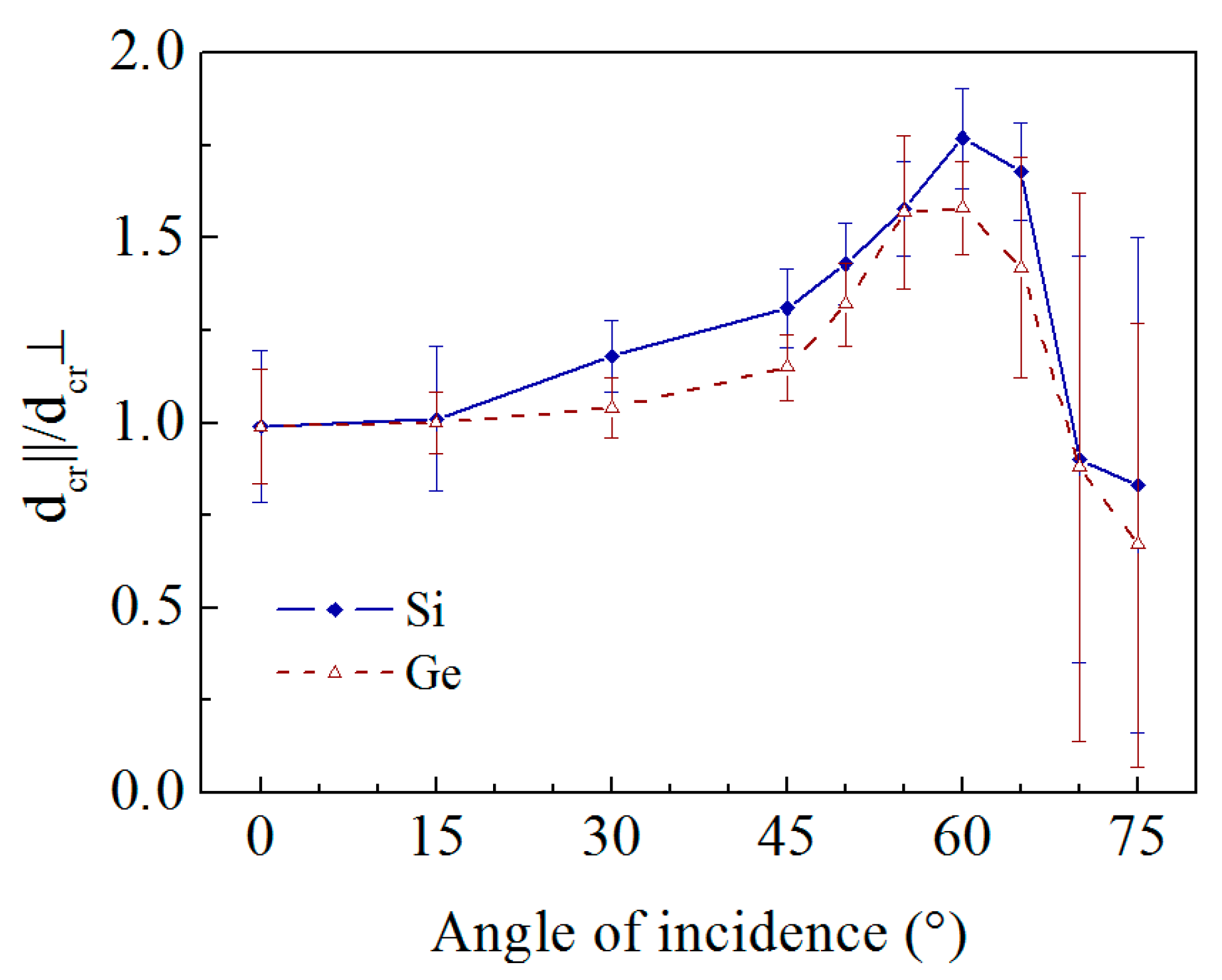
Considering the tendency of craters to narrow under oblique incidence, it is informative to analyze the crater diameter ratio of dcr∥/dcr⟂, shown in Figure 6. Although the absolute values of crater diameters differ between Si and Ge, their dcr∥/dcr⟂ ratios are relatively similar. The incidence angles of 55–60° correspond to the maximum dcr∥/dcr⟂ ratios of 1.8 for Si and 1.6 for Ge. These differences in hillock height and crater characteristics between silicon and germanium most likely arise from silicon’s lower atomic mass and density, combined with its higher Young’s modulus [46,47].
Figure 6.
Angular dependences of the crater diameter ratio of dcr∥/dcr⟂ for Si and Ge targets.
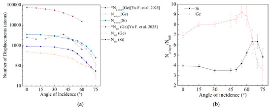
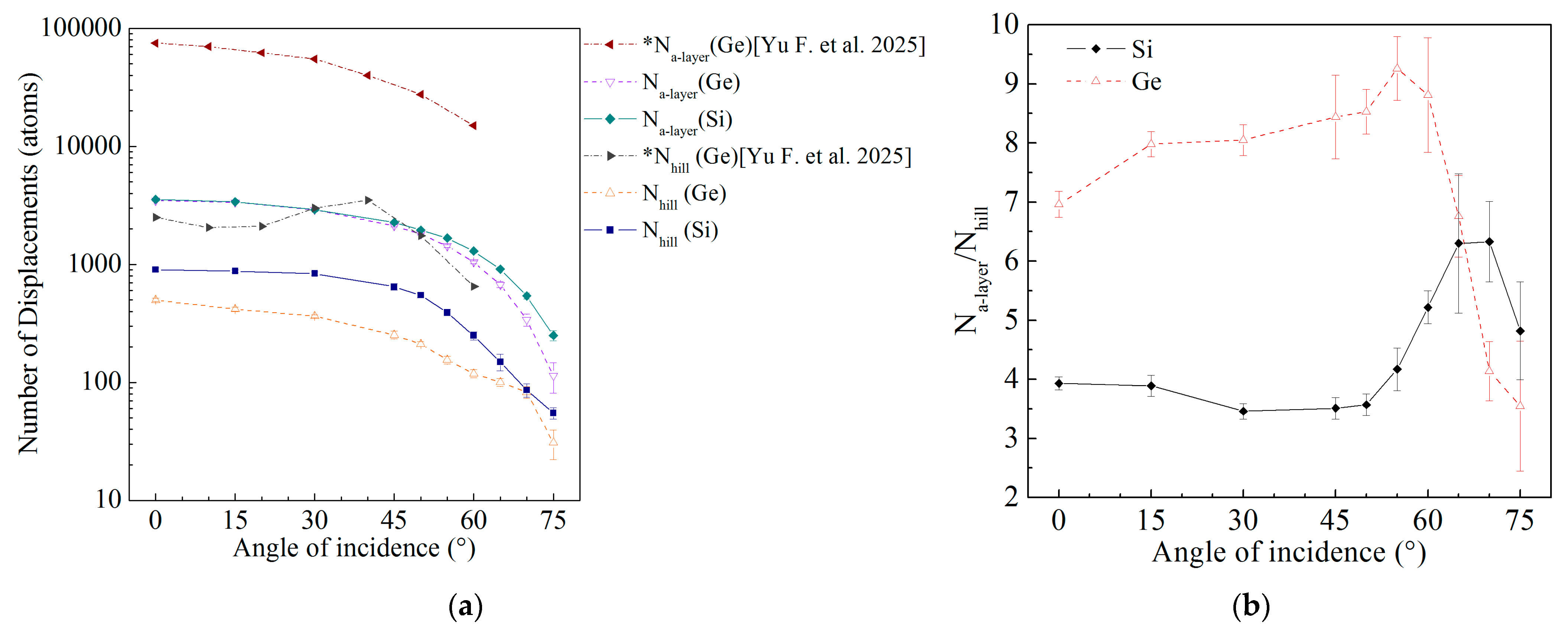
Figure 7 presents the angular dependences of the number of displacements after Ar923 cluster impact on Si and Ge targets. For clarity, the total number of displacements was separated into contributions below and above the surface, corresponding to the number of atoms in the amorphous region Na-layer and in the hillock Nhill, respectively. Notably, both materials exhibit nearly identical values of Na-layer up to 50°. However, beginning at 55°, the difference increases rapidly, reaching a factor of 1.2–2.2 in favor of silicon. As can be seen in Figure 7, the difference in the number of hillock atoms Nhill between Si and Ge persists over the entire angular range and amounts to a factor of 1.5–2.6.
Figure 7.
Angular dependences of the number of displacements in the amorphized layer Na-layer and hillock Nhill (a), and the displacement ratio of Na-layer/Nhill (b) after Ar923 cluster impact on Si and Ge targets. “*” indicates adjusted data relative to the local surface normal for consistent comparison [27].
Error bars representing the standard deviations (SD) of crater dimensions for different azimuthal incidence angles are shown in Figure 4, Figure 5 and Figure 6. The SD does not exceed 10% at small oblique angles and remains below 20% at incidence angles greater than 60°. The analysis indicates that the geometric characteristics of the impact craters are essentially independent of the azimuthal incidence angle. This suggests that the outcomes of cluster impact are largely insensitive to the crystallographic orientation of the target for both Si and Ge. This behavior can be explained by the fact that the crater size, and thus the impact area, significantly exceeds the lattice constants (0.566 nm for Ge and 0.543 nm for Si).
Comparison with the results of Yu et al. [27] (Figure 7a) indicates that increasing the cluster energy E leads to a substantial rise in the number of displaced atoms into the volume—by approximately 15–20 times for Ge. At the same time, higher energy also markedly increases the number of atoms displaced above the surface, by about 5–8 times. These comparisons should, however, be interpreted with caution because of differences in simulation conditions. Our silicon data agree well with those reported in Ref. [17], where the total number of displaced Si atoms at normal incidence of 10 keV Ar1000 cluster was about 4000.
Figure 7b shows the angular dependences of the ratio of the number of displaced atoms in the amorphous layer to the number of atoms in the hillock Na-layer/Nhill after Ar923 cluster impact on the Si and Ge surfaces. The maximum displacement ratio for silicon is reached at 65° and amounts to ~6.3, whereas for germanium a gradual increase is observed up to a maximum value of 9.3 at 55°. Over the entire angular range up to 65°, the displacement ratio for germanium exceeds that for silicon. This indicates that germanium accumulates a larger fraction of the deposited energy within the bulk, whereas silicon redistributes mass toward the surface more efficiently.
It should be noted that the intermediate transition between the maximum number of displacements and the onset of a sharp decrease in displacements occurs in the angular range of 40–60° (Figure 7a), while the maxima of the displacement ratios lie in the range of 55–65° (Figure 7b). These observations suggest that the morphological characteristics exhibiting distinctive behavior within the 50–65° interval may represent prerequisites for efficient surface nanostructuring, since this range corresponds to experimentally established optimal incidence angles for nanostructure formation [2,40,41,42,43].
3.2. Energy Characterization
In addition to the impact crater depth and amorphization depth, Figure 3 shows the potential energy Ep of the target atoms after impact, represented using a colormap. It should be noted that, despite the similarities between silicon and germanium, the potential energy Ep of Si and Ge atoms differs substantially both in bulk (−4.62 eV for Si and −3.85 eV for Ge) and at the surface (−2.6 eV for Si and −2.0 eV for Ge). The potential energy of atoms in the initial target volume corresponds to the cohesive energy Ecoh of silicon and germanium [48,49,50].
It should be emphasized that, in contrast to surface bombardment by a monomer, cluster impact does not lead to the formation of a region characterized by a radially decreasing and spatially uniform distribution of deposited energy—commonly referred to as the “core of deposited energy”. Within such a region (typical for monomer impact), a small number of highly energetic atoms transfer energy to the surrounding atoms and subsequently cool down. Energy profiles for 250 eV and 1500 eV Rn, Xe, Kr, and Ar bombardment of Si and Ge are presented in Ref. [51]. As one can see in Figure 3, the energy of atoms in the amorphized region of the target after cluster impact is distributed more chaotically due to the collective nonlinear interaction between cluster and target atoms [2,30,52,53].
Table 1 presents the average potential energy Ep of atoms within the amorphized volumes of the targets after cluster impact, standard deviation in all cases is about 0.15 eV. As can be seen in Table 1, the potential energy Ep of atoms in the amorphized volume changes by approximately 0.5 eV at normal incidence for both materials. With increasing incidence angle, the average potential energy Ep of the displaced target atoms remains nearly constant, but begins to vary noticeably from 65° for silicon and from 60° for germanium. It should be noted that at grazing incidence angles (≥70°), most of the displaced atoms within the amorphized region are surface atoms whose potential energy Ep differs significantly from the initial Ep after cluster impact (Table 1). This effect probably accounts for the observed surface activation effects [54].
Table 1.
Average potential energy of target atoms in the amorphized Si and Ge regions.
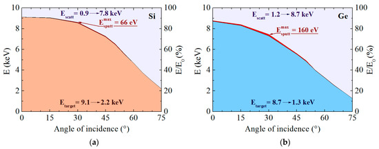
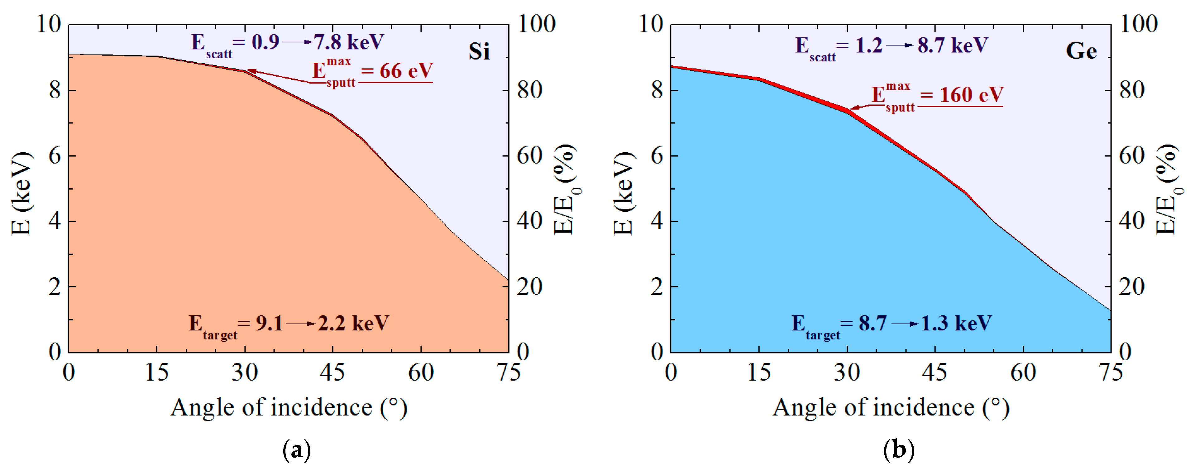
Figure 8 illustrates the redistribution of the total kinetic energy of the cluster E0 among target Etarget, scattered cluster atoms Escatt, and sputtered target atoms Esputt as a function of the angle of incidence. Under identical conditions, the energy transferred to the target Etarget is consistently higher for Si than for Ge. This can be attributed to the greater crater depth in Si and, consequently, to a larger energy deposition depth. This difference becomes more pronounced with increasing cluster incidence angle. The higher Etarget values in Si lead to a greater number of atoms displaced toward the surface (Figure 7a). At large angles of incidence (above 45°), a sharp decrease in the energy transferred to the target Etarget is observed, indicating a reduction in the penetration depth and an increase in the contribution of surface processes. These data correspond to a sharp decrease in the depths of the amorphous layer and the impact crater (Figure 4). The energy transferred to the Ge atoms Etarget also decreases with increasing angle of incidence, but the decline is more pronounced.
Figure 8.
Redistribution of the cluster kinetic energy E0 into the energy transferred to the target Etarget, the energy of scattered cluster atoms Escatt, and the energy of sputtered target atoms Esputt for Si (a) and Ge (b) after 55 ps at incidence angles from 0° to 75°.
Compared to Si, bombardment of germanium yields higher energies of scattered cluster atoms Escatt across the entire angular range. In contrast to Etarget, the smaller impact crater formed in Ge results in fewer collisions among cluster atoms and between cluster and target atoms, and consequently in a larger fraction of the original kinetic energy being retained. Thus, the mass of the target atoms likely plays a more significant role than the binding energy, leading to the predominance of elastic collisional dissipation of atomic energy.
Under all conditions, relatively lower values of sputtered energy Esputt are observed for Si, which can also be attributed to the difference in atomic masses between Si and Ge. As can be seen in Figure 8, the fraction of energy of sputtered target atoms Esputt constitutes only a small fraction of the initial kinetic energy of the cluster E0, and it is several orders of magnitude lower than the energy transferred to the target Etarget. These data are in good agreement, in terms of order of magnitude, with our previous results for SiO2 [29].
Based on the general form of the kinetic energy redistribution dependencies, three angular interaction regimes can be distinguished:
- (1)
- Volumetric braking: 0–30°, where the Etarget/E0 fraction dominates;
- (2)
- Transient regime: 30–55°, characterized by pronounced energy redistribution;
- (3)
- Surface regime: above 55°, where the Escatt/E0 fraction dominates.
It is worth noting that the low Escatt/E0 fraction at the normal cluster incidence is valid for both single-component semiconductor materials and metals. For example, for copper, when exposed to a high-energy small cluster, 20 keV Ar24, (E/N = 833 eV/atom) is approximately 7% [23].
This study considers individual cluster impacts on a flat target surface at various incidence angles, which obviously does not fully represent realistic experimental or technological conditions. However, the following factors should be emphasized. First, typical technological applications, such as surface smoothing or nanostructure formation, require ion fluences on the order of 1015–1016 clusters/cm2. This corresponds to several thousand consecutive random cluster impacts within the typical target dimensions. Simulating such conditions would require prohibitively large computational costs and, to the best of our knowledge, has not yet been implemented. Second, the forcedly small size of simulation cells—typically on the order of several tens of nanometers—restricts the ability to accurately reproduce real surface morphology. In practice, the lateral dimensions of surface irregularities (typically detected by AFM) exceed the dimensions accessible in MD simulations. Third, cluster impacts at different incidence angles on a flat surface can be interpreted as equivalent to real conditions of impacts on various regions of a rough surface (e.g., peaks, slopes, and valleys) characterized by different local incidence angles. Therefore, the present results provide meaningful insight into the fundamental mechanisms of cluster–surface interactions and remain relevant for practical applications of GCIB.
4. Conclusions
A comparative molecular dynamics study of 10 keV Ar923 cluster impact on Si and Ge surfaces in the angular range from 0° to 75° has been performed, focusing on crater formation, amorphization, number of displacements and energy redistribution. For the first time, the redistribution of the total kinetic energy of the cluster among target, scattered cluster atoms, and sputtered target atoms as a function of the angle of incidence is determined for silicon and germanium.
At small incidence angles, the impact crater is deeper and the amorphized layer is thicker in Si than in Ge. The deeper penetration of cluster energy into Si results in a larger fraction of energy being transferred to the target Etarget and leads to the formation of a more pronounced hillock. At the same time, the crater diameter in Ge is larger than that in Si.
At more oblique incidence angles, the difference in the transferred energy Etarget between Si and Ge becomes greater. As energy deposition shifts toward the near-surface region, the differences in penetration depth between Si and Ge diminish, and the crater and amorphization depths become comparable. However, the crater in Si remains more well-defined, with significantly larger lateral dimensions. This convergence may explain the experimentally observed similarity in ripple parameters formed on Si and Ge under oblique irradiation conditions, suggesting that comparable subsurface damage characteristics contribute to analogous surface nanopatterning. At the same time, silicon forms a larger hillock, indicating more efficient upward mass transport over the entire angular range.
Energy characterization shows that cluster impact does not produce a classical radially decaying “core of deposited energy”, typical for monomer bombardment. Instead, energy is distributed chaotically within the amorphized region due to collective nonlinear interactions between cluster and target atoms.
The most pronounced morphological and energetic transformations occur within 50–65°, which coincides with experimentally established optimal angles for nanostructure formation. This angular interval appears to represent a critical regime where subsurface damage, mass redistribution, and energy dissipation reach conditions favorable for efficient surface nanopatterning.
Overall, the results demonstrate that, although silicon and germanium exhibit qualitatively similar angular trends under cluster irradiation, quantitative differences in crater morphology, displacement statistics, and energy partitioning arise from intrinsic material properties. These findings provide insight into the mechanisms governing cluster–solid interactions and are relevant for efficiency calculations, radiation damage modeling, and surface nanostructuring.
Author Contributions
Conceptualization, I.V.N. and N.G.K.; methodology, I.V.N. and P.V.S.; validation, I.V.N. and P.V.S.; formal analysis, I.V.N., P.V.S. and N.G.K.; investigation, I.V.N., P.V.S. and N.G.K.; data curation, I.V.N. and P.V.S.; writing—original draft preparation, I.V.N. and P.V.S.; writing—review and editing, N.G.K. and A.B.T.; visualization, I.V.N. and P.V.S.; supervision, N.G.K. and A.B.T.; project administration, N.G.K.; funding acquisition, I.V.N. and N.G.K. All authors have read and agreed to the published version of the manuscript.
Funding
This work was funded by the Russian Science Foundation [Grant Number: 23-79-10061] (https://rscf.ru/en/project/23-79-10061/).
Institutional Review Board Statement
Not applicable.
Informed Consent Statement
Not applicable.
Data Availability Statement
The original contributions presented in this study are included in the article. Further inquiries can be directed to the corresponding authors.
Acknowledgments
The authors acknowledge the Novosibirsk State University Computer Center for providing supercomputer facilities.
Conflicts of Interest
The authors declare no conflicts of interest.
References
- Xie, K.G.; Xie, Y.; Deng, H. Gas Cluster Ion Beam Smoothing Technique: A Review. Nanomanuf. Metrol. 2025, 8, 12. [Google Scholar] [CrossRef] [Scilit]
- Ieshkin, A.E.; Tolstoguzov, A.B.; Korobeishchikov, N.G.; Pelenovich, V.O.; Chernysh, V.S. Gas-dynamic sources of cluster ions for basic and applied research. Phys. Usp. 2022, 65, 677–705. [Google Scholar] [CrossRef] [Scilit]
- Popok, V.N.; Barke, I.; Campbell, E.E.B.; Meiwes-Broer, K.-H. Cluster–surface interaction: From soft landing to implantation. Surf. Sci. Rep. 2011, 66, 347–377. [Google Scholar] [CrossRef] [Scilit]
- Yamada, I. Materials Processing by Cluster Ion Beams: History, Technology and Applications, 1st ed.; CRC Press: London, UK, 2015; 260p. [Google Scholar]
- Toyoda, N.; Yamada, I. Gas cluster ion beam equipment and applications for surface processing. IEEE Trans. Plasma Sci. 2008, 36, 1471–1488. [Google Scholar] [CrossRef] [Scilit]
- Insepov, Z.; Hassanein, A.; Norem, J.; Swenson, D.R. Advanced surface polishing using gas cluster ion beams. Nucl. Instrum. Methods Phys. Res. Sect. B Beam Interact. Mater. At. 2007, 261, 664–668. [Google Scholar] [CrossRef] [Scilit]
- Allen, L.P.; Fenner, D.B.; Santeufemio, C.; Brooks, W.; Hautala, J.; Shao, Y. Nano-scale surface texturing by impact of accelerated condensed-gas nanoparticles. Proc. SPIE 2002, 4806, 225–232. [Google Scholar] [CrossRef] [Scilit]
- Mahoney, C.M. Cluster Secondary Ion Mass Spectrometry: Principles and Applications, 1st ed.; John Wiley & Sons: New York, NY, USA, 2013. [Google Scholar]
- Delcorte, A.; Moshkunov, K.; Debongnie, M. Relationships between crater and sputtered material characteristics in large gas cluster sputtering of polymers: Results from molecular dynamics simulations. J. Vac. Sci. Technol. B 2018, 36, 03F109. [Google Scholar] [CrossRef] [Scilit]
- Delcorte, A.; Delmez, V.; Dupont-Gillain, C.; Lauzin, C.; Jefford, H.; Chundak, M.; Poleunis, C.; Moshkunov, K. Large cluster ions: Soft local probes and tools for organic and bio surfaces. Phys. Chem. Chem. Phys. 2020, 22, 17427–17447. [Google Scholar] [CrossRef] [Scilit]
- Cristaudo, V.; Poleunis, C.; Laha, P.; Eloy, P.; Hauffman, T.; Terryn, H.; Delcorte, A. Ion yield enhancement at the organic/inorganic interface in SIMS analysis using Ar-GCIB. Appl. Surf. Sci. 2021, 536, 147716. [Google Scholar] [CrossRef] [Scilit]
- Finšgar, M. Advanced surface analysis using GCIB-C60++-tandem-ToF-SIMS and GCIB-XPS of 2-mercaptobenzimidazole corrosion inhibitor on brass. Microchem. J. 2020, 159, 105495. [Google Scholar] [CrossRef] [Scilit]
- Takahashi, K.; Aoyagi, S.; Kawashima, T. TOF-SIMS matrix effects in mixed organic layers in Ar cluster ion depth profiles. Surf. Interface Anal. 2017, 49, 721–727. [Google Scholar] [CrossRef] [Scilit]
- Lorenz, M.; Shard, A.G.; Counsell, J.D.P.; Hutton, S.; Gilmore, I.S. Angular distribution of molecules sputtered by gas cluster ion beams and implications for secondary neutral mass spectrometry. J. Phys. Chem. C 2016, 120, 25317–25327. [Google Scholar] [CrossRef] [Scilit]
- Moritani, K.; Kanai, M.; Goto, K.; Ihara, I.; Inui, N.; Mochiji, K. Secondary ion emission from insulin film bombarded with methane and noble gas cluster ion beams. Nucl. Instrum. Methods Phys. Res. Sect. B Beam Interact. Mater. At. 2013, 315, 300–303. [Google Scholar] [CrossRef] [Scilit]
- Nakayama, Y.; Houzumi, S.; Toyoda, N.; Mochiji, K.; Mitamura, T.; Yamada, I. Irradiation of silicon surface by Ar cluster ion beam. Nucl. Instrum. Methods Phys. Res. Sect. B Beam Interact. Mater. At. 2005, 241, 618–621. [Google Scholar] [CrossRef] [Scilit]
- Aoki, T.; Matsuo, J.; Takaoka, G. Molecular dynamics study of damage formation characteristics by large cluster ion impacts. Nucl. Instrum. Methods Phys. Res. Sect. B Beam Interact. Mater. At. 2003, 202, 278–282. [Google Scholar] [CrossRef] [Scilit]
- Aoki, T.; Seki, T.; Matsuo, J. Molecular dynamics simulations for gas cluster ion beam processes. Vacuum 2010, 84, 994–998. [Google Scholar] [CrossRef] [Scilit]
- Samela, J.; Nordlund, K.; Popok, V.N.; Campbell, E.E.B. Origin of complex impact craters on native oxide coated silicon surfaces. Phys. Rev. B 2008, 77, 075309. [Google Scholar] [CrossRef] [Scilit]
- Allen, L.P.; Insepov, Z.; Fenner, D.B.; Santeufemio, C.; Brooks, W.; Jones, K.S.; Yamada, I. Craters on silicon surfaces created by gas cluster ion impacts. J. Appl. Phys. 2002, 92, 3671–3678. [Google Scholar] [CrossRef] [Scilit]
- Nordlund, K.; Samela, J. Atomic flows, coronas and cratering in Au, Si and SiO2. Nucl. Instrum. Methods Phys. Res. Sect. B Beam Interact. Mater. At. 2009, 267, 1420–1423. [Google Scholar] [CrossRef] [Scilit]
- Cheng, Y.Y.; Lee, C.C. Molecular dynamics simulations of argon cluster impacts on a nickel film surface. Nucl. Instrum. Methods Phys. Res. Sect. B Beam Interact. Mater. At. 2009, 267, 1428–1431. [Google Scholar] [CrossRef] [Scilit]
- Nazarov, A.V.; Zavilgelskiy, A.D.; Ieshkin, A.E.; Kireev, D.S.; Shemukhin, A.A.; Chernysh, V.S.; Nordlund, K.; Djurabekova, F. On the angular distributions of atoms sputtered by gas cluster ion beam. Vacuum 2023, 212, 112061. [Google Scholar] [CrossRef] [Scilit]
- Tian, J.; Zhou, W.; Feng, Q.; Zheng, J. Molecular dynamics simulations with electronic stopping can reproduce experimental sputtering yields of metals impacted by large cluster ions. Appl. Surf. Sci. 2018, 435, 65–71. [Google Scholar] [CrossRef] [Scilit]
- Paruch, R.J.; Garrison, B.J.; Mlynek, M.; Postawa, Z. On universality in sputtering yields due to cluster bombardment. J. Phys. Chem. Lett. 2014, 5, 3227–3230, Correction in J. Phys. Chem. Lett. 2014, 5, 3435. https://doi.org/10.1021/jz501979z. [Google Scholar] [CrossRef] [Scilit] [PubMed]
- Insepov, Z.; Yamada, I.; Sosnowski, M. Sputtering and smoothing of metal surface with energetic gas cluster beams. Mater. Chem. Phys. 1998, 54, 234–237. [Google Scholar] [CrossRef] [Scilit]
- Yu, F.; Zhang, T.; Chen, G.; Zhang, P.; Lu, H.; Cao, Y.; Ren, L.; Shao, H.; Zhao, X. Directional protrusion effect of Ge surface induced by argon cluster oblique bombardment. J. Appl. Phys. 2025, 138, 233104. [Google Scholar] [CrossRef] [Scilit]
- Zhou, Z.; Cui, J.; Hou, Q.; Zhang, K. Role of mass redistribution on nanoripple formation and propagation: A molecular dynamics simulation study. Appl. Surf. Sci. 2022, 585, 152630. [Google Scholar] [CrossRef] [Scilit]
- Korobeishchikov, N.G.; Stishenko, P.V.; Nikolaev, I.V.; Yakovlev, V.V. Silica sputtering by noble gas projectiles: Elucidating the effect of cluster species with molecular dynamic simulation. Plasma Chem. Plasma Process. 2022, 42, 1223–1235. [Google Scholar] [CrossRef] [Scilit]
- Nikolaev, I.V.; Stishenko, P.V.; Yakovlev, V.V.; Korobeishchikov, N.G. Effect of gas cluster species on crater formation for fused silica. J. Non-Cryst. Solids 2023, 619, 122590. [Google Scholar] [CrossRef] [Scilit]
- Thompson, A.P.; Aktulga, H.M.; Berger, R.; Bolintineanu, D.S.; Brown, W.M.; Crozier, P.S.; in ’t Veld, P.J.; Kohlmeyer, A.; Moore, S.G.; Nguyen, T.D.; et al. LAMMPS—A flexible simulation tool for particle-based materials modeling at the atomic, meso, and continuum scales. Comput. Phys. Commun. 2022, 271, 108171. [Google Scholar] [CrossRef] [Scilit]
- Rutkai, G.; Thol, M.; Span, R.; Vrabec, J. How well does the Lennard-Jones potential represent the thermodynamic properties of noble gases? Mol. Phys. 2017, 115, 1104–1121. [Google Scholar] [CrossRef] [Scilit]
- Ramírez, R.; Herrero, C.P. Quantum path-integral study of the phase diagram and isotope effects of neon. J. Chem. Phys. 2008, 129, 204502. [Google Scholar] [CrossRef] [Scilit]
- White, J.A. Lennard-Jones as a model for argon and test of extended renormalization group calculations. J. Chem. Phys. 1999, 111, 9352–9356. [Google Scholar] [CrossRef] [Scilit]
- Tersoff, J. Empirical interatomic potential for silicon with improved elastic properties. Phys. Rev. B 1988, 38, 9902–9905. [Google Scholar] [CrossRef] [Scilit]
- Ziegler, J.F.; Biersack, J.P.; Littmark, U. The Stopping and Range of Ions in Matter; Pergamon Press: New York, NY, USA, 1985; Volume 1. [Google Scholar]
- Bahn, S.R.; Jacobsen, K.W. An object-oriented scripting interface to a legacy electronic structure code. Comput. Sci. Eng. 2002, 4, 56–66. [Google Scholar] [CrossRef] [Scilit]
- Korobeishchikov, N.G.; Nikolaev, I.V.; Atuchin, V.V.; Prosvirin, I.P.; Kapishnikov, A.V.; Tolstogouzov, A.; Fu, D.J. Quantifying the surface modification induced by the argon cluster ion bombardment of KGd(WO4)2:Nd single crystal. Mater. Res. Bull. 2023, 158, 112082. [Google Scholar] [CrossRef] [Scilit]
- Korobeishchikov, N.G.; Nikolaev, I.V.; Atuchin, V.V.; Prosvirin, I.P.; Tolstogouzov, A.; Pelenovich, V.; Fu, D.J. Borate nonlinear optical single crystal surface finishing by argon cluster ion sputtering. Surf. Interfaces 2021, 27, 101520. [Google Scholar] [CrossRef] [Scilit]
- Toyoda, N.; Tilakaratne, B.; Saleem, I.; Chu, W.-K. Cluster beams, nano-ripples, and bio applications. Appl. Phys. Rev. 2019, 6, 020901. [Google Scholar] [CrossRef] [Scilit]
- Korobeishchikov, N.G.; Nikolaev, I.V.; Stishenko, P.V.; Yakovleva, M.V. Comparative nanopatterning of single-component semiconductors using oblique argon cluster ion bombardment. Mater. Sci. Semicond. Proc. 2025, 200, 110016. [Google Scholar] [CrossRef] [Scilit]
- Lozano, O.; Chen, Q.Y.; Tilakaratne, B.P.; Seo, H.W.; Wang, X.M.; Wadekar, P.V.; Chinta, P.V.; Tu, L.W.; Ho, N.J.; Wijesundera, D.; et al. Evolution of nanoripples on silicon by gas cluster-ion irradiation. AIP Adv. 2013, 3, 062107. [Google Scholar] [CrossRef] [Scilit]
- Korobeishchikov, N.G.; Nikolaev, I.V.; Lapega, A.V. Efficient nanopatterning of Ge surface induced by oblique argon cluster ion beam. Mater. Lett. 2024, 368, 136710. [Google Scholar] [CrossRef] [Scilit]
- Stukowski, A. Visualization and analysis of atomistic simulation data with OVITO—The Open Visualization Tool. Model. Simul. Mater. Sci. Eng. 2009, 18, 015012. [Google Scholar] [CrossRef] [Scilit]
- Kumar, T.; Kumar, A.; Agarwal, D.C.; Lalla, N.P.; Kanjilal, D. Ion beam-generated surface ripples: New insight in the underlying mechanism. Nanoscale Res. Lett. 2013, 8, 336. [Google Scholar] [CrossRef] [Scilit]
- Hopcroft, M.A.; Nix, W.D.; Kenny, T.W. What is the Young’s Modulus of Silicon? J. Microelectromech. Syst. 2010, 19, 229–238. [Google Scholar] [CrossRef] [Scilit]
- Swarnakar, A.K.; Van der Biest, O.; Van Humbeeck, J.; Vanhellemont, J. Determination of the single crystal Ge Young’s modulus between room temperature and melting temperature using the impulse excitation technique. Phys. Status Solidi C 2014, 11, 1566–1569. [Google Scholar] [CrossRef] [Scilit]
- Tersoff, J. Modeling solid-state chemistry: Interatomic potentials for multicomponent systems. Phys. Rev. B 1989, 39, 5566–5568, Erratum in Phys. Rev. B 1990, 41, 3248. https://doi.org/10.1103/PhysRevB.41.3248.2. [Google Scholar] [CrossRef] [Scilit] [PubMed]
- Farid, B.; Godby, R.W. Accurate exchange-correlation energy for the electron gas. Phys. Rev. B 1991, 43, 14248–14251. [Google Scholar] [CrossRef] [Scilit]
- Monteverde, U.; Migliorato, M.A.; Pal, J.; Powell, D. Assessment of empirical interatomic potentials for modeling semiconductor materials. J. Phys. Condens. Matter 2013, 25, 425801. [Google Scholar] [CrossRef] [Scilit]
- Hossain, M.Z.; Freund, J.B.; Johnson, H.T. Ion impact energy distribution and sputtering of Si and Ge. J. Appl. Phys. 2012, 111, 103513. [Google Scholar] [CrossRef] [Scilit]
- Nazarov, A.V.; Chernysh, V.S.; Zavilgelsky, A.D.; Shemukhin, A.A.; Lopez-Cazalilla, A.; Djurabekova, F.; Nordlund, K. The cluster species effect on the noble gas cluster interaction with solid surfaces. Surf. Interfaces 2021, 26, 101397. [Google Scholar] [CrossRef] [Scilit]
- Sirotkin, V. Molecular dynamic simulation of rutile surface bombardment by argon cluster ions. Vacuum 2021, 189, 110255. [Google Scholar] [CrossRef] [Scilit]
- Toyoda, N.; Sasaki, T.; Yamada, I.; Suga, T. Surface activation and planarization with gas cluster ion beam for wafer bonding. Electrochem. Soc. Trans. 2016, 75, 9–13. [Google Scholar] [CrossRef] [Scilit]

Disclaimer/Publisher’s Note: The statements, opinions and data contained in all publications are solely those of the individual author(s) and contributor(s) and not of MDPI and/or the editor(s). MDPI and/or the editor(s) disclaim responsibility for any injury to people or property resulting from any ideas, methods, instructions or products referred to in the content. |
© 2026 by the authors. Licensee MDPI, Basel, Switzerland. This article is an open access article distributed under the terms and conditions of the Creative Commons Attribution (CC BY) license.