


Highlights
- RF sputtering power governs growth regimes in NiOx thin films.
- Electrical resistivity exhibits a non-monotonic dependence on RF sputtering power.
- Preferred orientation shifts from (111) to (200) with increasing sputtering power.
- Comparison with dip-coating and AACVD reveals distinct structure–property trade-offs.
Abstract
Nickel oxide (NiOx) thin films are promising p-type transparent semiconductors for optoelectronic and energy-conversion devices. This study investigates the role of radio-frequency (RF) sputtering power in the growth evolution, microstructural development, and functional properties of NiOx thin films deposited at room temperature. The RF sputtering power was varied from 75 to 150 W, while the deposition time was adjusted to maintain an approximately constant thickness of ~110 nm. The films were characterized by atomic force microscopy (AFM), scanning electron microscopy (SEM), X-ray diffraction (XRD), optical transmittance, and electrical measurements. AFM and SEM analyses revealed an evolution from relatively smooth surfaces at low RF sputtering powers toward increased surface roughness at higher powers. XRD confirmed polycrystalline NiOx with a face-centered cubic structure, showing a preferential orientation shift from (111) to (200) and a maximum crystallite size of 14.73 nm at 125 W. Electrical resistivity showed a non-monotonic dependence on RF sputtering power, ranging from 25.39 to 309.85 kΩ·cm, indicating that the electrical response cannot be explained solely by crystallite size. Thickness-dependent analysis revealed an evolution from early-stage nucleation toward more developed columnar growth. Finally, comparison with dip-coating and AACVD revealed distinct structure–property relationships among the deposition routes.
1. Introduction
Nickel oxide (NiOx) is a p-type semiconductor that has attracted considerable attention due to its excellent chemical stability, optical transparency, and tunable electrical properties. Its wide bandgap, typically ranging from 3.4 to 4.3 eV depending on the synthesis route and processing conditions, makes it a promising material for optoelectronic and energy-conversion applications, including transparent electronics and photovoltaic devices [1,2]. Furthermore, its high optical transmittance in the visible region and good environmental stability make NiOx particularly attractive as a transparent functional layer.
NiOx thin films have been extensively investigated for applications in photovoltaic cells, electrochromic devices, gas sensors, ultraviolet photodetectors, and transparent electronics [3,4]. In these applications, the device performance strongly depends on the film microstructure, crystallographic orientation, optical properties, and electrical transport characteristics. In particular, the electrical conductivity of NiOx is closely associated with its defect chemistry, microstructure, and stoichiometry, which are influenced by the deposition conditions [5,6]. Consequently, understanding how processing parameters affect film growth and the resulting structure–property relationships remain essential for optimizing NiOx-based devices. Beyond conventional semiconductor thin films, two-dimensional (2D) semiconducting materials have also attracted considerable attention as functional materials, particularly for sensing applications, where their composition and electronic structure can be tailored to enhance their response to specific species [7].
Several physical and chemical deposition methods have been employed to fabricate NiOx thin films, including sol–gel spin-coating, chemical vapor deposition, thermal evaporation, dip-coating, aerosol-assisted chemical vapor deposition (AACVD), and sputtering techniques [8,9]. Among these methods, radio-frequency (RF) magnetron sputtering is particularly attractive because it enables reproducible deposition of dense oxide films at relatively low substrate temperatures while offering precise control over deposition parameters such as sputtering power, working pressure, and gas composition [10,11]. These characteristics make RF sputtering especially suitable for applications requiring uniform films and compatibility with temperature-sensitive substrates.
Despite the extensive literature on RF-sputtered NiOx thin films, previous studies have primarily focused on optimizing deposition parameters to improve individual properties such as crystallinity, optical transmittance, electrical conductivity, or device performance. However, comparatively less attention has been devoted to establishing a comprehensive correlation between RF sputtering power, growth-regime evolution, microstructural development, crystallographic orientation, and the resulting functional properties while minimizing the influence of film thickness [1,12].
At room temperature, thermal diffusion is limited, and the energy delivered by sputtered species becomes an important factor influencing adatom mobility, nucleation, grain coalescence, and defect formation [11,13]. Consequently, RF sputtering power plays a critical role in determining the transition between different growth regimes, which ultimately influences the film morphology, crystallographic texture, optical response, and electrical transport. Nevertheless, these phenomena are strongly interconnected, and the relationship between sputtering power, growth evolution, and the resulting functional properties has not yet been fully established.
In addition, although several deposition techniques have been reported for NiOx thin films, direct comparisons are often complicated by significant differences in film thickness, which is itself known to strongly affect the structural, optical, and electrical properties of thin films. Therefore, maintaining comparable film thicknesses provides a more reliable basis for evaluating the influence of the deposition route on the resulting structure–property relationships.
In this context, the present work systematically investigates the influence of RF sputtering power on the growth evolution, microstructural development, optical properties, and electrical transport of NiOx thin films deposited at room temperature while maintaining an approximately constant film thickness. By combining AFM, SEM, XRD, optical transmittance, optical band-gap determination, and electrical measurements, the study establishes correlations among RF sputtering conditions, morphological evolution, crystallographic orientation, optical response, and electrical behavior. Furthermore, thickness-dependent growth was investigated at fixed RF sputtering powers to provide complementary insight into the evolution of the film microstructure during deposition. Finally, NiOx thin films prepared by RF sputtering were compared with films deposited by dip-coating and AACVD at comparable film thicknesses. This comparative analysis provides an additional perspective on the structure–property relationships associated with different deposition routes and processing conditions, including the room-temperature deposition employed for RF sputtering and the elevated-temperature processing used for the reference films. The comparison is intended to highlight the structural and functional characteristics of the different approaches rather than to establish a performance ranking among the deposition techniques. These findings provide a more comprehensive understanding of the influence of RF sputtering conditions and film thickness on the structural and functional properties of NiOx thin films for optoelectronic and energy-related applications.
2. Experimental and Characterization Methods
In this work, NiOx thin films were deposited on glass substrates (0.9 mm Corning 2947N, Corning Incorporated, Corning, NY, USA) and p-type boron-doped silicon wafers (resistivity: 5–10 Ω·cm, orientation: (100), thickness: 279 ± 20 µm) using an RF magnetron sputtering system (AJA International Inc. Hingham, MA, USA).
A commercially available ceramic NiOx target with a purity of 99.99% and dimensions of 2 in. in diameter and 0.125 in. in thickness was used as the sputtering source. Prior to deposition, the chamber was evacuated to a base pressure of 1 mTorr. After reaching the base pressure, pure argon was introduced at a flow rate of 9 sccm, and the total working pressure was adjusted to 6 mTorr. No pre-sputtering or target-conditioning procedure was performed. The target-to-substrate distance was 25 mm, and the substrates were rotated during deposition. Prior to deposition, the substrates were cleaned by ultrasonic agitation in trichloroethylene (TCE) for 10 min, followed by ultrasonic cleaning in acetone for 10 min. The substrates were then rinsed with deionized water and dried by centrifugation. The substrate temperature was monitored using the sensor integrated into the sputtering system and remained approximately 27 °C throughout the deposition process. The experiments were performed in a temperature-controlled cleanroom. A commercially available ceramic NiOx target was used as the sputtering source. The films were deposited at room temperature under a total working pressure of 6 mTorr, using pure argon at a flow rate of 9 sccm as the sputtering gas. No oxygen was intentionally introduced into the chamber during the deposition process; therefore, the NiOx ceramic target was the primary oxygen source during film deposition. The working pressure, argon flow rate, and substrate temperature were kept constant throughout the experiments, while the deposition time was adjusted for each RF sputtering power to obtain a nearly constant film thickness of approximately 110 nm. Therefore, RF sputtering power was treated as the primary experimental variable, while the associated variation in deposition time was considered in the interpretation of the results.
RF magnetron sputtering was selected because it provides a stable plasma and is particularly suitable for the deposition of insulating and semiconducting oxide materials such as NiOx. In contrast to DC sputtering, RF excitation enables the deposition of oxide materials while mitigating charge accumulation on the target surface, thereby promoting plasma stability and deposition reproducibility. Furthermore, RF sputtering allows oxide thin films to be deposited at room temperature while providing precise control over the deposition parameters. This capability is particularly advantageous for systematically evaluating the influence of sputtering power on the growth regime, microstructural evolution, and functional properties of NiOx thin films.
For comparison purposes, NiOx thin films were also deposited by dip-coating (DC) and aerosol-assisted chemical vapor deposition (AACVD). Dip-coated films (~100 nm) were prepared from a methanolic solution of nickel acetate tetrahydrate and deposited onto glass substrates at a withdrawal rate of 3 cm min−1 for eight cycles, followed by thermal annealing at 500 °C for 1 h. AACVD films (~115 nm) were grown at 450 °C from a precursor solution of nickel acetate in deionized water with acetic acid, using N2 as the carrier gas at a flow rate of 5 L min−1.
The morphological, structural, electrical, and optical properties of the NiOx films were systematically investigated using atomic force microscopy (AFM), scanning electron microscopy (SEM), X-ray diffraction (XRD), electrical current–voltage (I–V) measurements, and optical transmittance spectroscopy. Optical transmittance measurements were performed using an MProbe system (SemiconSoft Inc., Southborough, MA, USA) in the 300–900 nm wavelength range.
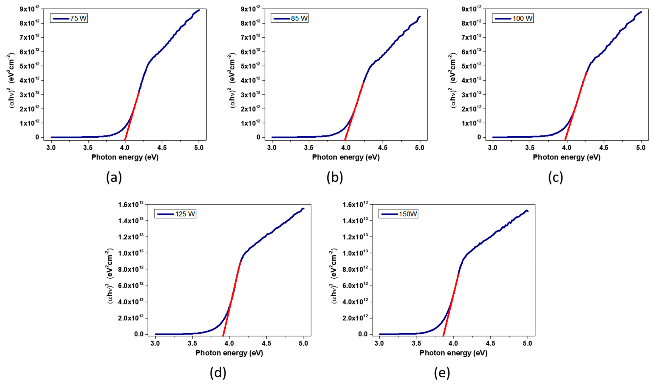
The optical band gap (Eg) was determined using the Tauc method by considering a direct allowed transition. The transmittance data were converted from wavelength to photon energy using hν = 1240/λ, where hν is expressed in eV and λ in nm. The absorption coefficient was then calculated from the transmittance data, and the corresponding Tauc plots of (αhν)2 vs. hν were constructed. For each sample, the fitting interval was manually selected by identifying the approximately linear region associated with the absorption edge. The selected region was fitted by linear regression using OriginPro 9.0, and the fitting quality was evaluated using the coefficient of determination R2. A criterion of R2> 0.998 was used to ensure a highly linear correlation for all reported fits. The fitted line was subsequently extrapolated to (αhν)2 = 0, and the intercept with the photon-energy axis was taken as the optical band gap Eg.
For the electrical characterization, 150 nm-thick Au electrical contacts were deposited by thermal evaporation in a Leybold Univex 300 vacuum chamber (Leybold GmbH, Cologne, Germany). The contacts were defined using a 2 cm × 2 cm shadow mask containing two four-pad configurations. Each configuration consisted of four circular Au pads with a diameter of 1.414 mm and a center-to-center spacing of 4 mm. Electrical resistance (R) was determined from the slope of linear current–voltage (I–V) curves measured using a two-point probe configuration. The voltage was swept from −1 to +1 V in 0.01 V increments. The electrical resistivity (ρ) was calculated from the measured resistance by considering the coplanar circular contact geometry according to Equation (1):
where t is the film thickness, R is the resistance obtained from the slope of the I–V curve, r is the radius of contacts (0.707 mm), and d is the center-to-center distance between contacts (4 mm).
The current–voltage (I–V) data were analyzed by linear regression using OriginPro. The electrical resistance was obtained from the inverse of the slope of the linear I–V fit, R = 1/b, where b is the slope of the I vs. V relationship. Representative I–V characteristics and the corresponding linear fits are provided in Supplementary Figure S1.
AFM surface topography was analyzed using the Roughness Analysis tool implemented in WSxM (https://wsxm.eu/). The analysis was performed on the complete AFM topography maps, rather than on individual linear profiles. The AFM images were acquired over an area of approximately 2 × 2 µm2 with a resolution of 256 × 256 pixels. Prior to the roughness analysis, the images were processed using plane correction and simple flattening. Surface topography was quantitatively characterized using the arithmetic mean height (Sa), root-mean-square height (Sq), surface skewness (Ssk), and surface kurtosis (Sku). For each sputtering condition, one AFM topography map was analyzed.
Surface and cross-sectional morphologies were examined using a DualBeam FIB-SEM system Scios (FEI Company, Hillsboro, OR, USA). Surface SEM images were acquired at an accelerating voltage of 5 kV, a working distance of approximately 6.9 mm, and magnifications up to 100,000× to analyze grain distribution and surface morphology. Cross-sectional FIB-SEM images were obtained after focused ion beam (FIB) milling. Prior to FIB milling, a protective Pt layer was deposited on the NiOx surface to protect the film during preparation of the cross section. A rough cross section was then milled using the Ga+ ion beam, followed by a cleaning step to improve the quality of the exposed cross section. Cross-sectional images were acquired using the secondary electron detector (ETD) at an accelerating voltage of 2 kV and a working distance of 6.8 mm, allowing detailed observation of film thickness, columnar growth, and the film–substrate interface. Film thickness was determined by direct dimensional measurement of the NiOx layer in the cross-sectional SEM images, measuring the distance between the upper film surface and the NiOx/substrate interface while excluding the protective Pt layer. An estimated measurement uncertainty of ±1.0 nm was considered for the thickness determination and is reported throughout the manuscript. Because Ga+—based FIB milling can introduce artifacts such as ion implantation, localized amorphization, surface modification, and redeposition, these potential effects were considered when interpreting the cross-sectional images. SEM and FIB-SEM measurements were performed under high-vacuum conditions.
X-ray diffraction (XRD) analyses were carried out using a PANalytical X’Pert PRO diffractometer (PANalytical B.V., Almelo, The Netherlands) equipped with a Cu Kα radiation source (λ = 1.541874 Å), operated at 45 kV and 20 mA. Measurements were performed in grazing-incidence reflection geometry with an incidence angle of Ω = 1°, employing a parabolic W/Si mirror in the incident beam path. Data were collected over a 2θ range of 20–100°, with a step size of 0.04° and a counting time of 0.5 s per step.
3. Results and Discussion
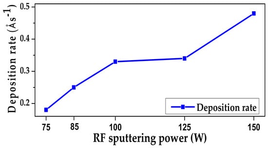
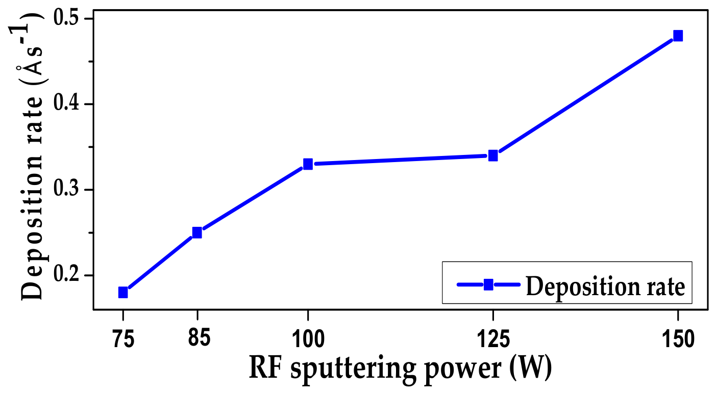
Table 1 and Figure 1 show the deposition rate of the films as a function of RF sputtering power. The deposition rate increases overall with increasing RF sputtering power, from approximately 0.184 ± 0.002 Å s−1 at 75 W to 0.483 ± 0.004 Å s−1 at 150 W. A comparatively small increase is observed between 100 W (0.332 ± 0.003 Å s−1) and 125 W (0.338 ± 0.003 Å s−1). This limited variation indicates that the deposition rate does not increase linearly over the entire power range. Such behavior may reflect the combined influence of the sputtering conditions and the deposition-time adjustment used to obtain approximately comparable film thicknesses. Therefore, the deposition-rate data are interpreted as an experimental trend rather than as evidence of a strictly linear dependence on RF sputtering power.
Table 1.
Deposition time, thickness and deposition rate as a function of RF sputtering power for NiOx thin films.
Figure 1.
Deposition rate as a function of RF sputtering power for NiOx thin films.
In sputtering processes, increasing applied power can increase the sputtering yield and the flux of material reaching the substrate [10]. Under the room-temperature conditions employed in this study, these changes in the deposition environment may also influence adatom mobility and the subsequent evolution of the film microstructure [13]. However, because RF sputtering power and deposition time were coupled in the main experimental series, the observed structural changes cannot be attributed exclusively to RF sputtering power. Moreover, because plasma characteristics and ion-energy distributions were not directly measured, changes in energetic particle flux and ion bombardment are considered possible contributions rather than directly quantified mechanisms [14]. The influence of RF sputtering power on the surface morphology, crystallographic structure, electrical transport, and optical properties is therefore analyzed in the following sections using AFM, SEM, XRD, and electrical and optical measurements.
3.1. Effect of Sputtering Power on Surface Morphology
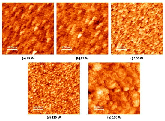
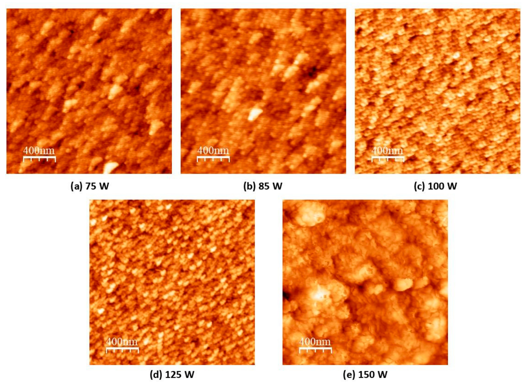
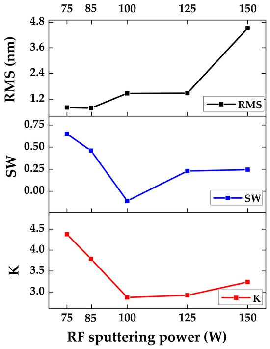
Figure 2 shows AFM height images of NiOx thin films deposited at different RF sputtering powers, highlighting the evolution of surface morphology with the deposition conditions. The AFM maps were analyzed over the complete scanned area using the Roughness Analysis tool in WSxM. At low RF sputtering powers of 75 and 85 W (Figure 2a,b), the films exhibit relatively smooth and homogeneous surfaces, with RMS roughness Sq values of 0.81 and 0.78 nm, respectively. The corresponding arithmetic mean roughness Sa values are 0.63 and 0.61 nm. The positive surface skewness values Ssk = 0.65 and 0.46 indicate a height distribution with a greater contribution from surface features above the mean plane, whereas the kurtosis values Sku = 4.39 and 3.80 indicate relatively pronounced tails in the height distributions. These results are consistent with surfaces exhibiting low overall height variation but localized nanoscale topographic features. The relatively low roughness observed at 75–85 W indicates that the films remain comparatively smooth under these deposition conditions. The corresponding areal surface topography parameters are summarized in Table 2.
Figure 2.
AFM height images of NiOx thin films deposited at different RF sputtering powers: (a) 75 W, (b) 85 W, (c) 100 W, (d) 125 W, and (e) 150 W. The AFM images were acquired over a 2 × 2 µm2 scan area with a resolution of 256 × 256 pixels.
Table 2.
Areal surface topography parameters of NiOx thin films deposited at different RF sputtering powers.
When the RF sputtering power increases to 100 W (Figure 2c), the RMS roughness increases to 1.47 nm, while Sa reaches 1.19 nm. At the same time, the surface skewness approaches zero Ssk = −0.11, indicating a more symmetric distribution of surface heights. The kurtosis decreases to Sku = 2.87, suggesting a narrower height distribution with fewer pronounced extreme features compared with the lower-power conditions. These changes indicate an evolution of the surface topography, with greater height variation but a more symmetric distribution of surface features. Such behavior is consistent with a transition in the surface growth morphology as the deposition conditions are modified by increasing RF sputtering power [15,16].
At higher RF sputtering powers of 125 and 150 W (Figure 2d,e), the surface morphology changes more markedly. The 125 W film exhibits an RMS roughness of 1.48 nm and an arithmetic mean roughness of 1.19 nm, whereas the 150 W film shows a substantially higher RMS roughness of 4.53 nm and Sa = 3.58 nm. The increase in Sq and Sa at 150 W indicates a pronounced increase in the amplitude of the surface-height variations. At 125 W, the slightly positive skewness Ssk = 0.23 and kurtosis close to 3 Sku = 2.92 indicate a relatively symmetric height distribution. At 150 W, Ssk remains positive (0.25), while Sku increases to 3.25, indicating a greater contribution from localized height variations and a broader distribution of surface features. The AFM results therefore indicate that increasing the RF sputtering power is associated with a progressive increase in surface roughness, particularly at 150 W.
Figure 3 summarizes the RMS roughness, surface skewness, and surface kurtosis as a function of RF sputtering power. According to the Thornton structure zone model [15], the morphology of sputtered films deposited at low substrate temperatures is strongly influenced by the balance between adatom mobility and the energy available during film growth. In the present study, all films were deposited at room temperature, so thermal diffusion is limited. The observed evolution from relatively smooth surfaces at 75–85 W toward greater surface-height variations at higher RF sputtering powers is therefore consistent with changes in the growth conditions and surface evolution associated with the sputtering process [10,16]. However, because RF sputtering power and deposition time were coupled in the main experimental series, the observed morphological changes cannot be attributed exclusively to RF sputtering power. The AFM results should therefore be interpreted as reflecting the combined influence of the associated deposition conditions on surface morphology.
Figure 3.
RMS, skewness, and kurtosis values as a function of RF sputtering power of NiOx thin films.
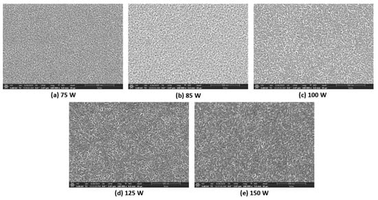
Figure 4 presents SEM top-view images that corroborate the AFM results, revealing a clear evolution of surface morphology with increasing sputtering power, consistent with changes in grain growth and surface diffusion. Films deposited at low powers (75 and 85 W, Figure 4a,b) exhibit highly uniform and compact surfaces composed of very fine grains that are difficult to distinguish individually, indicating a growth regime dominated by high nucleation density and limited surface diffusion. When the power increases to 100 W (Figure 4c), the grains become more distinguishable and slightly larger, suggesting enhanced adatom mobility and the onset of grain coalescence. At higher deposition powers (125 and 150 W, Figure 4d,e), the films develop more pronounced elongated grain-like features, together with a broader grain-size distribution and less uniform grain morphology. These features suggest a transition toward a higher-energy growth regime, where enhanced ion bombardment may promote increased adatom mobility, anisotropic growth, and surface restructuring.
Figure 4.
Top-view SEM images of NiOx thin films deposited at different RF sputtering powers: (a) 75 W, (b) 85 W, (c) 100 W, (d) 125 W, and (e) 150 W. The images were acquired at an accelerating voltage of 5 kV, a working distance of 6.9 mm, and a magnification of 100,000×. The scale bar corresponds to 500 nm.
Although the SEM images show relatively uniform surface morphologies, the AFM analysis reveals nanoscale variations in the surface-height distribution that may not be readily discernible in SEM images. In particular, skewness (SW) and kurtosis (K) are statistical parameters describing the distribution of surface heights and therefore provide information about the asymmetry and sharpness of the surface topography rather than directly quantifying the visual uniformity of the film [16]. Thus, variations in SW and K are not necessarily inconsistent with the relatively uniform morphology observed by SEM. The AFM and SEM results should therefore be considered complementary, providing quantitative topographical and morphological information, respectively [17].
3.2. Structural Evolution and Crystallinity
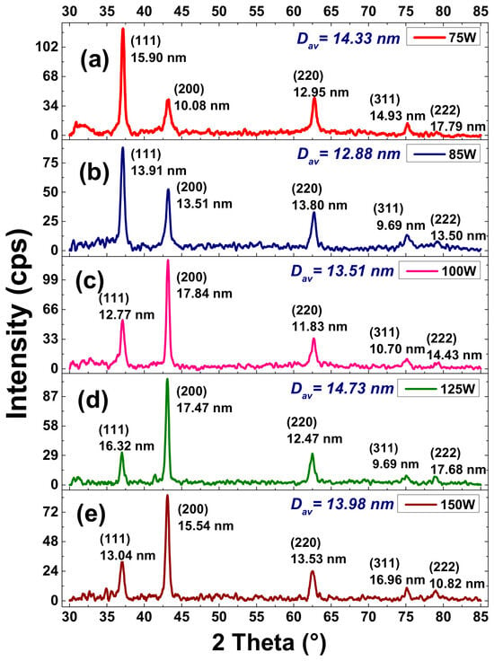
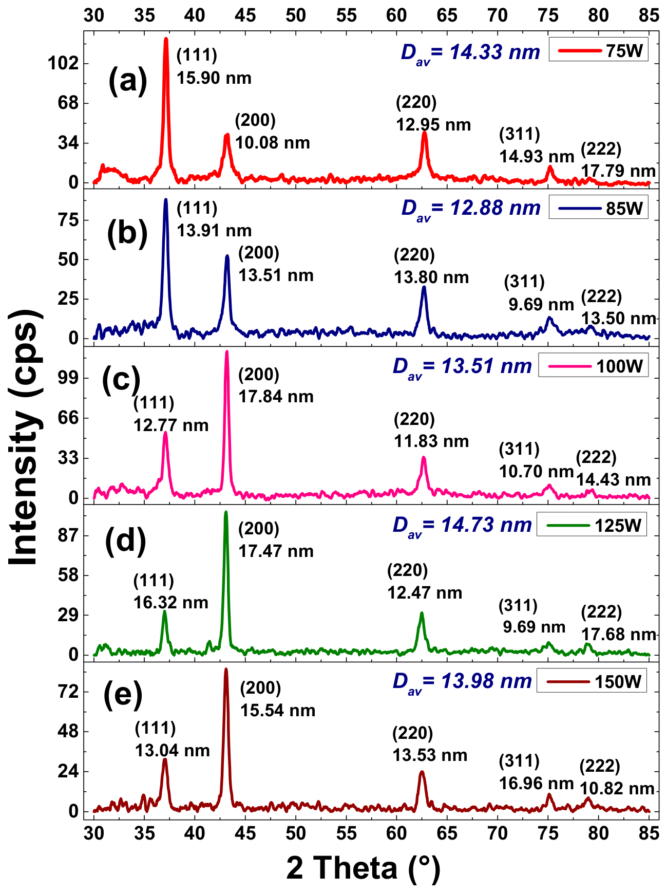
Figure 5 shows XRD patterns confirming the formation of polycrystalline NiOx with a face-centered cubic structure (JCPDS 65-2901), with well-defined diffraction peaks located at 37.14°, 42.95°, 62.53°, 76.87°, and 79.41°, corresponding to the (111), (200), (220), (311), and (222) planes, respectively.
Figure 5.
θ–2θ X-ray diffraction patterns of NiOx thin films deposited at different RF sputtering powers: (a) 75 W, (b) 85 W, (c) 100 W, (d) 125 W, and (e) 150 W.
At low sputtering powers of 75–85 W (Figure 5a,b), the films exhibit a preferred (111) orientation, which is commonly associated with surface energy minimization under low-energy growth conditions [14,15,18]. As the power increases to 100 and 125 W (Figure 5c,d), the preferred orientation gradually shifts toward the (200) plane. This reorientation is consistent with a change in the competitive growth mechanism among crystallographic planes associated with changes in adatom mobility [19,20]. The films deposited at 100 and 125 W exhibit the most intense and well-defined diffraction peaks, while the average crystallite size (Dₐᵥ) reaches its maximum at 125 W (Dₐᵥ = 14.73 nm, Figure 5d), suggesting more developed coherent crystalline domains under these deposition conditions. However, at 150 W (Figure 5e), the crystallite size decreases slightly despite the higher RF sputtering power. This behavior may be associated with changes in the balance between adatom mobility and energetic particle interactions during film growth, which could limit the development of coherent crystalline domains [19,21]. Therefore, the observed structural evolution suggests that increasing RF sputtering power does not necessarily result in a monotonic increase in crystallite development.
The preferred orientation of polycrystalline NiOx thin films can be influenced by several factors, including the substrate surface condition, film–substrate interface, deposition energy, and adatom mobility during the initial stages of growth [22,23]. In the present study, all samples were deposited on identical substrates under the same nominal pressure, gas-flow, and substrate-temperature conditions, with RF sputtering power selected as the primary experimental variable, while deposition time was adjusted to obtain approximately comparable film thicknesses. Therefore, the observed evolution from the (111) to the (200) preferred orientation is consistent with changes in the deposition conditions associated with increasing RF sputtering power, which may modify adatom mobility and the competitive growth of different crystallographic planes. Nevertheless, substrate surface termination and interface-related effects cannot be completely excluded, particularly during the initial stages of film nucleation and growth. Since the substrate surface termination and the initial interface structure were not independently characterized in this study, their possible contribution to the observed preferred orientation is acknowledged. The crystallite size evolution obtained from XRD is consistent with the morphological features observed by AFM and SEM, where increasing RF sputtering power is accompanied by grain coalescence and a progressive modification of surface roughness. These structural changes provide the basis for the electrical behavior discussed in the following section.
The evolution of the preferred orientation may also contribute to the electrical response of the films. The films deposited at 75 and 85 W exhibit a preferred (111) orientation, whereas the 100, 125, and 150 W films show a preferential contribution from the (200) reflection. However, the resistivity does not follow a simple relationship with this change in orientation. For example, the 75 and 85 W films exhibit the same preferred orientation but substantially different resistivities of 25.39 and 109.79 kΩ·cm, respectively. Similarly, the 100, 125, and 150 W films show a preferential (200) orientation while their resistivities vary from 58.98 to 309.85 kΩ·cm. These results indicate that preferred orientation may influence the electrical properties, but it cannot be considered the sole factor determining the observed resistivity. Instead, the electrical response should be interpreted considering the combined effects of crystallographic orientation, crystallite development, microstructure, and the associated deposition conditions.
3.3. Correlation Between Microstructure and Electrical Resistivity
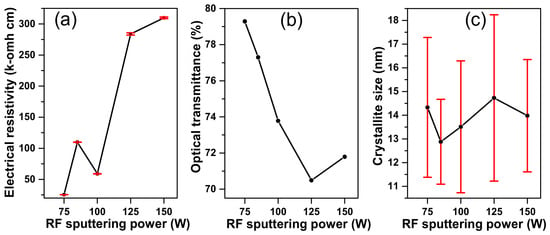
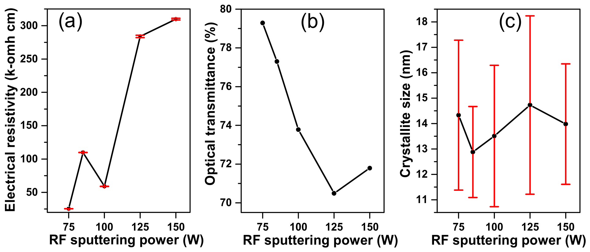
Figure 6 shows the electrical resistivity, optical transmittance, and crystallite size of NiOx thin films deposited at different RF sputtering powers. Error bars for electrical resistivity represent the uncertainty propagated from the standard error of the slope obtained from the linear I–V fitting. These uncertainties represent the uncertainty associated with the linear regression of the I–V data and should not be interpreted as sample-to-sample standard deviations. Error bars for crystallite size represent the standard deviation of the crystallite-size values calculated from the identified diffraction reflections. The optical transmittance values were obtained from individual spectral measurements for each sample. Because replicate measurements were not performed, a statistical uncertainty could not be reliably determined; therefore, no error bars were assigned to the transmittance data to avoid introducing an unsupported estimate. Because a two-point measurement configuration was employed, the contribution of contact resistance, current spreading, and contact inhomogeneity cannot be independently separated from the measured resistance. Therefore, the approximately linear I–V responses support the use of the linear-fit slope for resistance determination, but do not constitute an independent validation of ideal ohmic contacts.
Figure 6.
Dependence of (a) electrical resistivity, (b) optical transmittance, and (c) crystallite size of NiOx thin films on RF sputtering power.
Figure 6 reveals a non-monotonic dependence of electrical resistivity on RF sputtering power, indicating that the electrical transport properties are influenced by the structural and defect-related characteristics of the films. Electrical transport in NiOx has been described in the literature within a small-polaron hopping framework involving localized holes associated with Ni2+/Ni3+ states, with the carrier concentration and hopping probability influenced by defect-related characteristics [24,25,26]. In this context, the observed resistivity behavior is discussed within this established theoretical framework; however, the present measurements do not provide direct experimental evidence of the specific transport mechanism.
The lowest resistivity is obtained at 75 W (25.39 kΩ·cm), despite the relatively small average crystallite size. This observation indicates that crystallite size alone cannot account for the electrical transport behavior of the films. The electrical properties of NiOx have been associated with defect-related effects and microstructural characteristics, including Ni vacancies and Ni3+-related states reported for NiOx films [27,28]. In the present study, however, these defect states were not directly characterized; therefore, their possible contribution is discussed within the framework established in the literature rather than as an experimentally verified mechanism. At 85 W, the resistivity increases to 109.79 kΩ·cm, while the average crystallite size decreases to 12.88 nm. At 100 W, the resistivity decreases to 58.98 kΩ·cm despite the relatively small variation in average crystallite size. These results indicate that the electrical response cannot be explained solely by crystallite size or grain coalescence, but may also involve other microstructural characteristics of the films [29,30].
The films deposited at 125 and 150 W exhibit the highest resistivity values (283.85 and 309.85 kΩ·cm, respectively), while their average crystallite sizes remain comparable to that obtained at 75 W. The XRD results also show changes in the relative intensities of the diffraction peaks with RF sputtering power, indicating an evolution of the preferred crystallographic orientation. Preferred orientation and crystallite size represent distinct structural characteristics: the former is related to the relative intensities of the diffraction peaks, whereas the latter is determined from diffraction peak broadening. Changes in crystallographic texture can influence the structural and electrical properties of polycrystalline NiOx films [22,27,30]. Therefore, the observed variation in resistivity should not be attributed exclusively to crystallite size, but rather considered in relation to the combined structural characteristics of the films.
It should also be noted that the p-type character of the films was not directly determined in the present study. Although NiOx is widely reported as a p-type semiconductor and hole transport has been associated with Ni vacancies and Ni3+-related states in the literature [6], the present electrical measurements were limited to resistivity characterization and therefore do not provide direct information on carrier polarity, concentration, or mobility. Hall-effect or Seebeck measurements would be required to experimentally determine these parameters. Accordingly, the p-type transport framework is used here as a literature-supported interpretation rather than as an experimentally verified property of the present films.
Overall, the average crystallite size obtained in the present study does not exhibit a monotonic dependence on RF sputtering power, ranging from approximately 12.9 to 14.7 nm. The comparable crystallite sizes obtained at 75, 125, and 150 W, together with the lower values observed at 85 and 100 W, indicate that the structural evolution cannot be described solely by an increase in RF sputtering power. Previous studies have shown that sputtering conditions can influence crystallographic texture, crystallite development, and other structural characteristics of NiOx thin films [14,22,28]. In particular, Salunkhe et al. reported an increase in the average crystallite size with increasing sputtering power for NiOx films deposited by DC magnetron sputtering [28]. The different trend observed in the present RF-sputtered films may therefore arise from differences in the deposition configuration and associated processing conditions, including the plasma characteristics and deposition time. Although an increase in energetic particle flux with RF sputtering power may influence adatom mobility and crystallographic development, the present study does not include direct measurements of plasma characteristics, ion energy, substrate bias, or ion flux. Therefore, enhanced ion bombardment is considered a possible contribution to the observed structural evolution rather than a demonstrated mechanism [14]. The present results should consequently be interpreted in terms of changes in crystallite development and preferred orientation rather than as evidence of a universal increase or decrease in crystallinity with sputtering power.
3.4. Optical Properties and Their Structural Correlation
Figure 6 also shows the optical transmittance of the NiOx thin films as a function of RF sputtering power. The optical transmittance in the visible range (400–700 nm) varies between 73% and 79%, with the highest value observed at 75 W. A general decrease in transmittance is observed with increasing sputtering power, particularly up to 125 W. This behavior can be attributed to changes in film microstructure and defect-related optical absorption that may be associated with the deposition conditions. Variations in sputtering power may influence the microstructural characteristics and defect states of the films, which in turn may modify the optical absorption coefficient and light scattering [25,28].
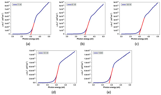
The optical band gap was determined from the transmittance data using Tauc plots, assuming a direct allowed transition. Figure 7 presents the corresponding Tauc plots for the NiOx films deposited at different RF sputtering powers, where the experimental curves are shown in blue and the linear fitting regions used for the extrapolation of Eg are shown in red. As summarized in Table 3, the optical band gap decreases systematically from 4.01 eV at 75 W to 3.86 eV at 150 W. The intermediate values are 4.00, 3.98, and 3.92 eV for films deposited at 85, 100, and 125 W, respectively. The high coefficients of determination obtained for the linear fits (R2 = 0.99845–0.99937) support the reliability of the extracted band-gap values.
Figure 7.
Tauc plots of NiOx thin films deposited at different RF sputtering powers: (a) 75 W; (b) 85 W; (c)100 W; (d) 125 W and (e)150 W. Colors: Experimental curves (blue lines), linear fits used for the extrapolation of the optical band gap (red lines).
Table 3.
Optical band gap values determined from Tauc plots for NiOx thin films deposited at different RF sputtering powers.
The progressive reduction in Eg with increasing sputtering power is consistent with modifications in the electronic structure associated with changes in the microstructure and defect-related states of the films. In particular, the increase in deposition energy can modify the growth conditions, crystallite development, and defect population, potentially introducing additional electronic states that influence the optical absorption edge. However, because the defect chemistry was not directly characterized in the present study, the observed decrease in Eg should be considered as being consistent with changes in defect-related states rather than as direct evidence of a specific defect species.
The optical and electrical properties do not exhibit a strictly correlated trend. Although the resistivity shows a non-monotonic dependence on sputtering power, the optical transmittance and band gap exhibit comparatively systematic variations with increasing power. This indicates that optimal optical transparency does not necessarily correspond to optimal electrical performance. Instead, the interplay among microstructural characteristics, defect-related states, crystallinity, and surface morphology contributes to the observed optical and electrical behavior of the NiOx thin films [18,31].
3.5. Thickness-Dependent Growth and Structural Evolution
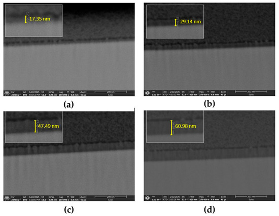
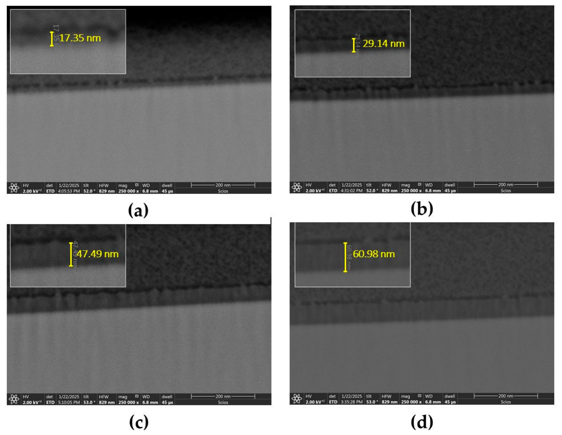
To investigate the thickness-dependent growth evolution of NiOx thin films, samples with different thicknesses (17–61 nm) were deposited at a fixed RF sputtering power of 125 W, while the deposition time was varied. The other nominal deposition conditions were maintained constant, including a working pressure of 6 mTorr, an argon flow rate of 9 sccm, and room temperature. This thickness-dependent series was designed to complement the RF sputtering-power analysis by examining the structural evolution of the films at a constant sputtering power. Figure 8 presents the cross-sectional FIB-SEM images of the films, revealing progressive changes in the film morphology with increasing thickness. At low thickness (~17 nm), the film corresponds to an early nucleation stage, characterized by an initially discontinuous morphology. As the thickness increases (~29 nm), the film becomes more continuous, suggesting the onset of island coalescence. At intermediate thickness (~47 nm), vertically oriented features begin to develop, indicating a transition toward a more developed columnar morphology. Finally, at higher thickness (~61 nm), a denser and more defined columnar structure is observed. This morphological evolution is consistent with a progressive nucleation, island coalescence, and development of columnar features as the film thickness increases, as reported for thin-film growth under comparable conditions [18,28,32]. However, the present cross-sectional observations alone do not establish a specific growth mechanism unequivocally.
Figure 8.
Cross-sectional FIB-SEM images of NiOx thin films deposited at 125 W RF sputtering power with different thicknesses: (a) 17.4 ± 1.0 nm, (b) 29.1 ± 1.0 nm, (c) 47.5 ± 1.0 nm, and (d) 61.0 ± 1.0 nm. The images were acquired using a secondary electron detector (ETD) at an accelerating voltage of 2 kV and a working distance of 6.8 mm. The scale bar is 200 nm.
To further investigate the influence of film thickness on the growth and structural evolution of NiOx thin films, additional thinner films were deposited at 125 and 150 W and compared with the corresponding films of approximately 110 nm used as reference. These two RF sputtering power conditions were selected because the deposition rate increases with RF sputtering power, allowing measurable variations in film thickness to be obtained within shorter deposition times. Thus, the 125 and 150 W conditions provided practical conditions for examining thickness-dependent changes in the film morphology and structure. The lower-power conditions (75–100 W) were not included in this thickness series because substantially longer deposition times would have been required to obtain comparable thickness variations. Therefore, the thickness-dependent analysis was intentionally focused on the 125 and 150 W conditions rather than on the complete RF sputtering power range.
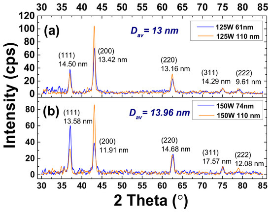
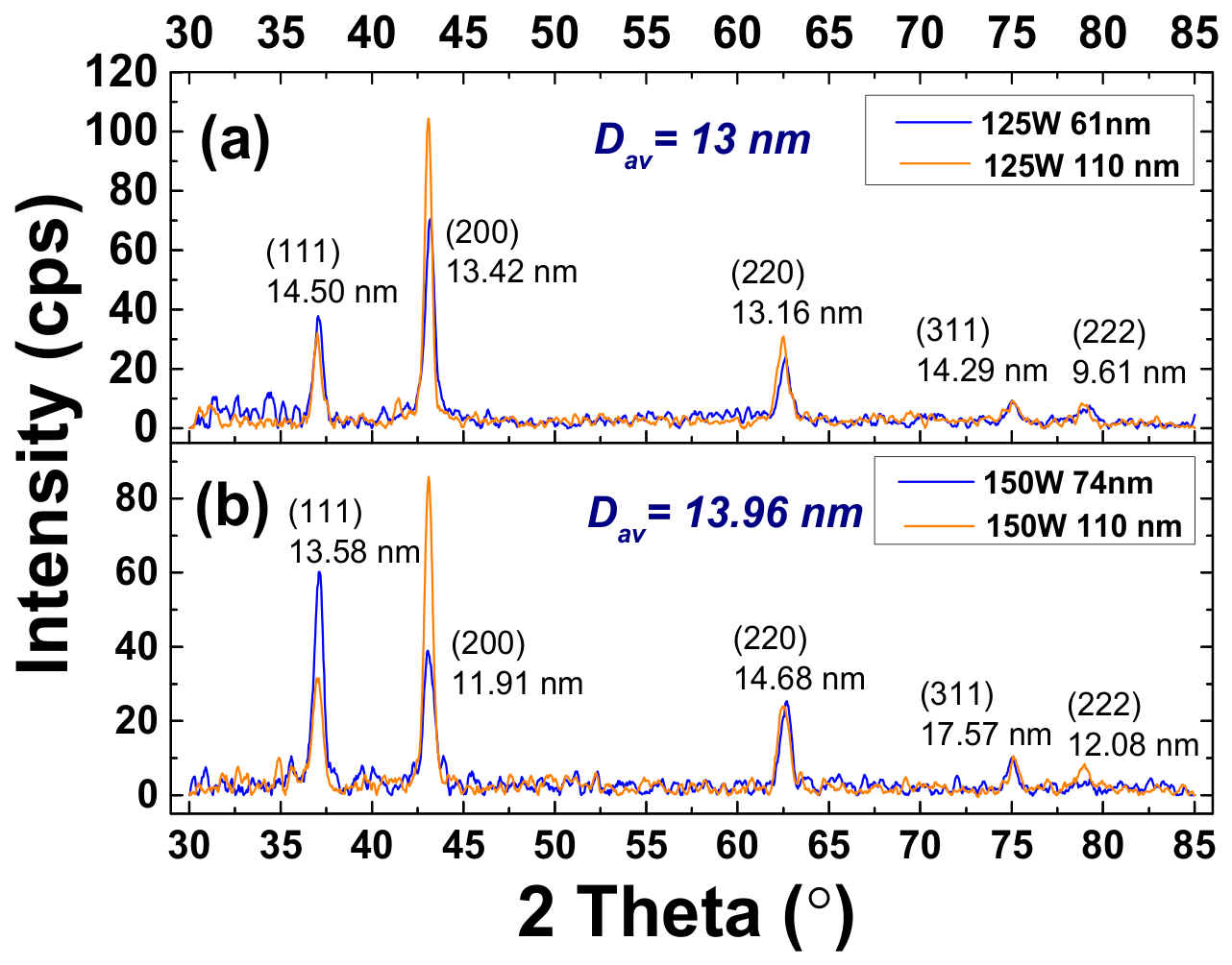
Figure 9 presents the θ–2θ X-ray diffraction patterns of NiOx thin films deposited by RF sputtering at different powers and thicknesses. The solid blue curves correspond to the thinner films deposited at 125 W, 61 nm and 150 W, 74 nm, whereas the orange curves correspond to the respective approximately 110-nm-thick films used as reference patterns. This comparison was performed to highlight the thickness-dependent structural evolution of the films. The results indicate that the structural development of NiOx films is influenced not only by RF sputtering power but also by film thickness, with the magnitude and nature of the thickness effect depending on the sputtering conditions. This behavior is consistent with the progressive development of the polycrystalline structure as the film thickness increases, including the morphological evolution observed from the early nucleation stage toward more developed columnar features [18,28,32].
Figure 9.
θ–2θ X-ray diffraction patterns of NiOx thin films deposited by RF sputtering at different powers and thicknesses: (a) 125 W, 61.0 ± 1.0 nm; (b) 150 W, 74.0 ± 1.0 nm. The corresponding approximately 110-nm-thick films are included as reference patterns.
The comparison between films of different thicknesses and their functional properties is summarized in Table 4. The results reveal thickness-dependent behavior, although strongly coupled with sputtering power. At 125 W, reducing the thickness from approximately 110 nm to 61 nm leads to an increase in resistivity and changes in the structural development of the film. This behavior may be associated with the less developed microstructure at the earlier stages of growth, where grain coalescence and the formation of continuous crystalline domains are still evolving [33,34]. In contrast, decreasing the thickness from approximately 110 nm to 74 nm results in lower resistivity but also reduced optical transmittance. Interestingly, the 150 W thickness series also exhibit a change in preferred crystallographic orientation: the 74-nm-thick film shows a stronger contribution from the (111) reflection, whereas the approximately 110-nm-thick film exhibits a stronger (200) contribution. This result suggests that the preferred orientation can evolve during film growth as the film thickness increases.
Table 4.
Electrical resistivity, optical transmittance, and crystallite size of NiOx thin films deposited by RF sputtering at different powers and thicknesses: 125 W, 61 nm; 125 W, 110 nm; 150 W, 74 nm; and 150 W, 110 nm.
The 150 W–74 nm film exhibits a crystallite size of Dav = 13.96 nm, which is very similar to that of the approximately 110-nm-thick film Dav = 13.98 nm. Therefore, the observed change in preferred orientation is not accompanied by a significant change in the average crystallite size. The lower resistivity of the 74-nm-thick film (71.71 kΩ·cm), compared with 309.86 kΩ·cm for the approximately 110-nm-thick film, coincides with the stronger (111) contribution. This correlation suggests that the evolution of crystallographic orientation may contribute to the electrical response; however, it does not establish a direct causal relationship because film thickness and deposition time were simultaneously varied.
Within each thickness comparison, the RF sputtering power, working pressure, Ar flow rate, and substrate temperature were kept constant, while the deposition time was adjusted to obtain the desired film thickness. Consequently, the observed structural and electrical differences should be interpreted as the combined effects of film thickness, growth stage, crystallographic orientation, and deposition time under the corresponding RF sputtering conditions.
Within each thickness comparison, the films were deposited under identical sputtering conditions, including RF sputtering power, pressure, Ar flow rate, and substrate temperature. The deposition time was the parameter adjusted to obtain different film thicknesses. Therefore, the 74 nm film represents an earlier growth stage, whereas the 110 nm film corresponds to a more advanced stage of film development. During film growth, microstructural evolution—including grain coalescence, densification, crystallinity, and defect distribution—progressively changes with deposition time. Consequently, although the 74 nm film is thinner, its optical response is also influenced by its microstructural evolution. Under the high-energy sputtering conditions employed at 150 W, these microstructural effects can compensate for, or even outweigh, the increase in transmittance expected solely from a reduced thickness. Together, these results indicate that thickness modifies crystallite size, optical transmittance, and electrical resistivity through changes in grain development, structural disorder, and defect distribution.
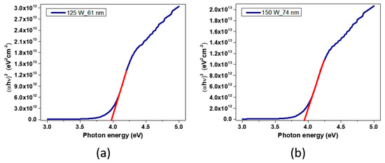
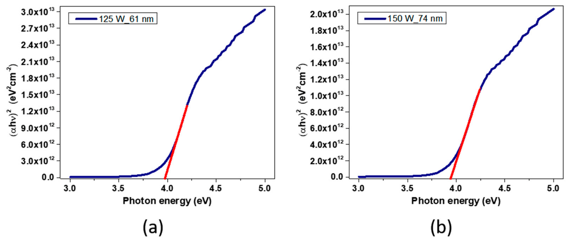
Figure 10 and Table 5 show the thickness-dependent optical band gap obtained from Tauc plots for the NiOx thin films deposited at 125 and 150 W. The 61 nm film deposited at 125 W exhibited an optical band gap of 3.98 eV, compared with 3.92 eV for the corresponding ~110 nm film. Similarly, the 74 nm film deposited at 150 W showed an optical band gap of 3.95 eV, compared with 3.86 eV for the ~110 nm film. Thus, reducing the thickness resulted in a slight increase in the optical band gap of 0.06 eV at 125 W and 0.09 eV at 150 W. Both thinner films exhibited direct allowed transitions, with high coefficients of determination for the linear fits (R2 = 0.99943 and 0.99823, respectively). These results indicate that the thickness-dependent variation in Eg is relatively small and should be interpreted together with the associated microstructural evolution and sputtering power.
Figure 10.
Tauc plots of NiOx thin films with different thicknesses (a) 61 nm (125 W), (b) 74 nm (150 W). Colors: Experimental curves (blue lines), linear fits used for the extrapolation of the optical band gap (red lines).
Table 5.
Optical band gap values determined from Tauc plots for NiOx thin films with different thicknesses.
Overall, these results indicate that film thickness influences the morphological and structural development of the films, including the evolution from an early nucleation stage toward more developed columnar features, while its effects on structural development, optical band gap, and electrical properties are strongly coupled with RF sputtering power.
3.6. Structure–Property Trade-Offs in NiOx Thin Films: A Comparative Study of Deposition Techniques
To establish a meaningful comparison among deposition techniques, NiOx thin films with comparable thicknesses of approximately 110–115 nm were intentionally prepared by RF sputtering, dip-coating (DC), and aerosol-assisted chemical vapor deposition (AACVD). The thickness was selected and controlled to minimize its contribution to the differences in microstructure and functional properties, allowing the influence of the deposition route to be examined more directly. This approach is particularly relevant because film thickness strongly affects nucleation, crystallite development, optical transmittance, and electrical resistivity, as demonstrated by the thickness-dependent results presented in Section 3.5. Therefore, the present comparison is not intended to establish a universal performance ranking among deposition techniques, but rather to identify the structure–property trade-offs associated with their distinct growth mechanisms under comparable film thicknesses.
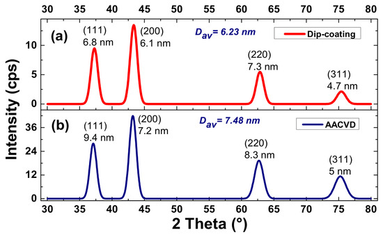
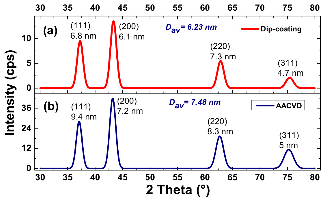
The comparison also highlights a fundamental difference in processing conditions. The RF-sputtered films were deposited entirely at room temperature, whereas the DC and AACVD films were processed at elevated temperatures of approximately 500 and 450 °C, respectively [13]. The room-temperature operation of RF sputtering is particularly relevant for temperature-sensitive substrates, polymeric or flexible materials, and device architectures in which thermal exposure must be minimized. Thus, the comparison provides not only a structure–property perspective but also a processing perspective, highlighting the potential of RF sputtering as a low-temperature route for NiOx thin-film fabrication. Figure 11 presents the θ–2θ X-ray diffraction patterns of NiOx thin films deposited by dip-coating and AACVD. The analysis reveals that RF-sputtered films exhibit significantly larger crystallite sizes (Dₐᵥ ≈ 13.9 nm) compared to those obtained by DC (≈ 6.2 nm) and AACVD (≈7.5 nm).
Figure 11.
θ–2θ X-ray diffraction patterns of NiOx thin films deposited by: (a) Dip-coating and (b) AACVD.
The XRD patterns obtained for the dip-coated and AACVD NiOx films were processed using the same data-treatment procedure. Savitzky–Golay smoothing was applied using a 51-point window and a second-order polynomial. A straight-line baseline determined from the mean intensity of the 1% end points was subtracted as part of the data-processing procedure. No additional smoothing was applied after this treatment.
Despite the elevated processing temperatures used for DC and AACVD, which can promote crystallization, these films exhibit smaller coherent crystallite domains under the conditions investigated here. In contrast, the RF-sputtered films exhibit larger crystallite domains despite being deposited at room temperature. This result demonstrates that relatively large crystalline domains can be obtained under room-temperature RF sputtering conditions. However, the difference in crystallite size cannot be attributed exclusively to the deposition technique, since the films were obtained using different processing routes and thermal histories. The observed structural differences should therefore be interpreted as the combined effect of the deposition method and the associated processing conditions.
The comparison also highlights a fundamental difference in processing conditions. The RF-sputtered films were deposited entirely at room temperature, whereas the DC and AACVD films were processed at elevated temperatures of approximately 500 and 450 °C, respectively. Therefore, the differences observed among the three deposition routes should be interpreted as the combined effect of the deposition technique and the associated processing conditions, particularly the growth or annealing temperature. The room-temperature operation of RF sputtering is particularly relevant for temperature-sensitive substrates, polymeric or flexible materials, and device architectures in which thermal exposure must be minimized. Thus, the comparison provides not only a structure–property perspective but also a processing perspective, highlighting the potential of RF sputtering as a low-temperature route for NiOx thin-film fabrication.
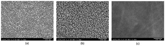
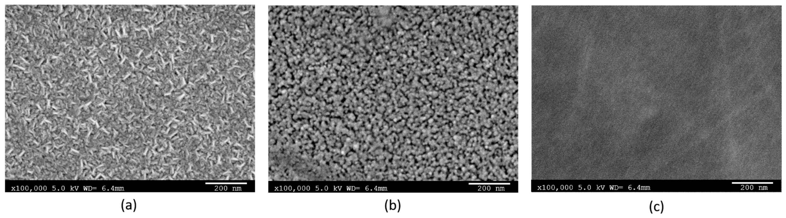
Figure 12 presents SEM top-view images of NiOx thin films deposited by RF sputtering, dip-coating, and AACVD, all with comparable thicknesses of approximately 110–115 nm. The images reveal clear differences in surface morphology among the three deposition routes. Dip-coated films exhibit a homogeneous surface composed of fine, closely packed grains, consistent with their smaller crystallite size. In contrast, RF-sputtered films display a denser morphology with elongated and coalesced features, consistent with the larger coherent crystallite domains observed by XRD. The AACVD films show a relatively uniform and smoother surface with reduced grain contrast, suggesting the presence of fine nanostructured domains. These differences indicate that the observed surface morphology and microstructural development depend on the deposition route and its associated processing conditions, even when the film thickness is comparable.
Figure 12.
Top-view SEM images of NiOx thin films deposited by different methods: (a) RF sputtering at 125 W, (b) dip-coating, and (c) AACVD. The images were acquired at an accelerating voltage of 5 kV, a magnification of 100,000×, and a working distance of approximately 6.4 mm. The scale bar corresponds to 200 nm.
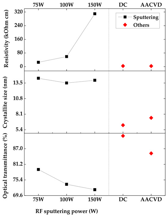
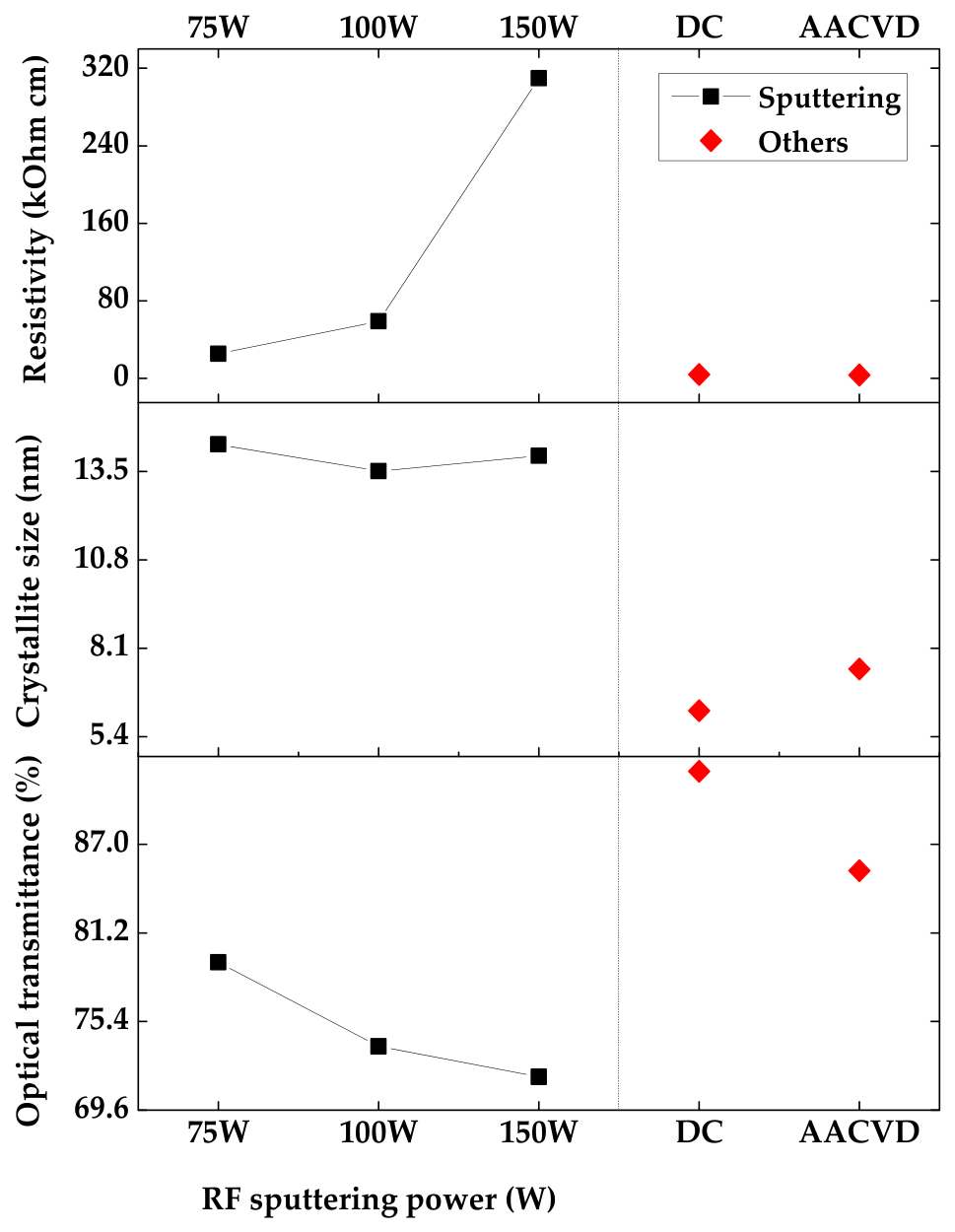
Figure 13 summarizes the electrical resistivity, optical transmittance, and crystallite size of NiOx thin films deposited by RF sputtering, dip-coating (DC), and AACVD. For the RF-sputtered films, resistivity spans a wide range from approximately 25 to 430 kΩ·cm, depending on sputtering power, whereas the crystallite size remains within a relatively narrow range of approximately 13–15 nm. Optical transmittance varies between approximately 65% and 80%, reflecting the combined influence of microstructure, surface morphology, and deposition conditions. In comparison, the DC and AACVD films exhibit substantially lower resistivity values of approximately 3–4 kΩ·cm, together with smaller crystallite sizes of approximately 6–7 nm and higher optical transmittance of approximately 85%–92%. These differences demonstrate that comparable film thickness does not result in equivalent functional properties, indicating that the deposition route and associated processing conditions influence the structure–property relationships of NiOx thin films.
Figure 13.
Electrical resistivity, optical transmittance, and crystallite size of NiOx thin films deposited by RF sputtering, dip-coating (DC) and AACVD.
The RF-sputtered films therefore occupy a distinct structure–property regime characterized by relatively large crystallite domains and dense microstructures, together with higher resistivity than the DC and AACVD films. The lower resistivity observed for the latter techniques may be associated with differences in defect states, stoichiometry, and microstructural development; however, direct identification of the underlying defect chemistry would require complementary chemical characterization [5]. Rather than indicating a universally superior deposition route, these results demonstrate that each technique provides a different balance between crystallite development, optical transparency, and electrical transport.
Overall, this comparative analysis demonstrates that the deposition and associated processing conditions influence the structure–property relationships of NiOx thin films, even when the film thickness is intentionally maintained at approximately 110 nm. The use of comparable thicknesses provides a controlled basis for distinguishing the effects of the deposition mechanism from those associated with thickness variations. RF sputtering offers a distinctive combination of room-temperature processing, relatively large crystallite domains, dense microstructures, and controllable electrical properties through adjustment of sputtering power. In particular, the ability to obtain crystalline and dense NiOx films without high-temperature processing is relevant for applications involving temperature-sensitive substrates. DC and AACVD, in contrast, provide higher optical transmittance and lower resistivity under the conditions examined here, but require elevated processing temperatures. Therefore, the results demonstrate that the appropriate deposition technique depends on the targeted balance between optical transparency, electrical transport, microstructural control, and processing temperature. The present comparison highlights RF sputtering as a versatile low-temperature route for tailoring NiOx thin films while providing a direct structure–property perspective relative to commonly used solution-based deposition techniques.
4. Conclusions
This study investigates the influence of RF sputtering power on the structural, morphological, optical, and electrical properties of NiOx thin films deposited at room temperature. The results show that changes in RF sputtering power are accompanied by modifications in surface morphology, crystallographic orientation, crystallite development, and electrical response. The films deposited at 75 and 85 W exhibit relatively smooth surfaces, whereas increasing the RF sputtering power, particularly to 150 W, results in a pronounced increase in surface roughness. XRD analysis confirms the polycrystalline face-centered cubic structure of NiOx and reveals an evolution of the preferred orientation from (111) at lower powers toward a stronger (200) contribution at higher powers. The average crystallite size does not exhibit a monotonic dependence on RF sputtering power, ranging from approximately 12.9 to 14.7 nm, with a maximum value of 14.73 nm at 125 W.
The electrical resistivity exhibits a non-monotonic dependence on RF sputtering power, ranging from 25.39 to 309.85 kΩ·cm. The observed electrical behavior cannot be explained solely by crystallite size, indicating that the electrical response is influenced by the combined structural characteristics and deposition conditions. Defect-related states and small-polaron transport are considered possible interpretations within the framework established in the literature; however, the present study does not provide direct experimental evidence of a specific defect chemistry or transport mechanism. Similarly, changes in energetic particle flux and ion bombardment may contribute to the observed structural evolution, but these effects were not directly measured and therefore cannot be established as the governing mechanism.
Thickness-dependent analysis further shows that the structural and electrical properties evolve during film growth. At 125 W, reducing the film thickness from approximately 110 to 61 nm increases the resistivity, whereas at 150 W, reducing the thickness from approximately 110 to 74 nm results in a substantial decrease in resistivity and coincides with a change in preferred crystallographic orientation from a stronger (200) contribution toward a stronger (111) contribution. Because deposition time was adjusted to obtain the different thicknesses, the effects of film thickness, growth stage, and deposition time are coupled in these comparisons. The observed cross-sectional and surface morphologies are consistent with progressive nucleation, coalescence, and development of columnar features during film growth; however, the present data do not allow a definitive assignment of a specific growth mode.
Comparison with dip-coating and AACVD films demonstrates distinct structure–property relationships among the deposition routes. The RF-sputtered films exhibit larger average crystallite sizes under the conditions investigated, together with distinct morphological and electrical characteristics. However, these differences should be interpreted considering the different deposition and thermal histories of the films. Overall, the results demonstrate that RF sputtering at room temperature provides a viable route for tailoring the structural and functional properties of NiOx thin films through control of the deposition conditions and film thickness.
Supplementary Materials
The following supporting information can be downloaded at: https://www.mdpi.com/article/10.3390/coatings16101129/s1, Figure S1: Current–voltage (I–V) characteristics of NiOₓ thin films deposited at different RF sputtering powers. Experimental data are shown together with the corresponding linear fits for: (a) 75 W, (b) 85 W, (c) 100 W, (d) 125 W, and (e) 150 W.
Author Contributions
Conceptualization: S.V.-y.-P. and I.C., formal analysis: S.V.-y.-P. and I.Á.S., investigation: S.V.-y.-P., methodology: S.V.-y.-P. and I.C., project administration: S.V.-y.-P. and I.C., supervision and validation: I.C. and S.M., writing—original draft: S.V.-y.-P., writing—review and editing: all authors, funding acquisition: I.C. All authors have read and agreed to the published version of the manuscript.
Funding
This research was funded by Mexican Ministry of Science, Humanities, Technology and Innovation (SECIHTI), postdoctoral fellowship under CVU 623020.
Institutional Review Board Statement
Not applicable.
Informed Consent Statement
Not applicable.
Data Availability Statement
The original contributions presented in this study are included in the article. Further inquiries can be directed to the corresponding author.
Acknowledgments
I. Alvarez Samario acknowledges financial support from SECIHTI 4044623. During the preparation of this work the authors used ChatGPT (GPT-5.6 Luna) in order to check redaction and language. After using this tool/service, the authors reviewed and edited the content as needed and take full responsibility for the content of the published article.
Conflicts of Interest
The authors declare no conflicts of interest.
References
- Nedev, R.; Mateos-Anzaldo, D.; Osuna-Escalante, E.; Perez-Landeros, O.; Curiel-Alvarez, M.; Osorio-Urquizo, E.; Castillo-Saenz, J.; Lopez-Medina, J.; Valdez-Salas, B.; Nedev, N. Effect of Deposition Temperature and Thermal Annealing on the Properties of Sputtered NiOx/Si Heterojunction Photodiodes. Inorganics 2025, 13, 11. [Google Scholar] [CrossRef] [Scilit]
- Song, Z.; Bourgeteau, T.; Raifuku, I.; Bonnassieux, Y.; Johnson, E.; Ishikawa, Y.; Foldyna, M.; i Cabarrocas, P.R.; Uraoka, Y. Structural study of NiOx thin films fabricated by radio frequency sputtering at low temperature. Thin Solid Films 2018, 646, 209–215. [Google Scholar] [CrossRef] [Scilit]
- Hossain, M.I.; Hasan, A.K.M.; Qarony, W.; Shahiduzzaman, M.; Islam, M.A.; Ishikawa, Y.; Uraoka, Y.; Amin, N.; Knipp, D.; Akhtaruzzaman, M.; et al. Electrical and Optical Properties of Nickel-Oxide Films for Efficient Perovskite Solar Cells. Small Methods 2020, 4, 2000454. [Google Scholar] [CrossRef] [Scilit]
- Kumar, C.; Donoso, B.; Silva, H.; Padilla-Campos, L.; Zarate, A. The enhanced light trapping nature of NiOx thin films deposited by magnetron sputtering onto silicon solar cells at room temperature. Mater. Lett. 2021, 297, 129961. [Google Scholar] [CrossRef] [Scilit]
- Liu, Y.-H.; Liu, X.-Y.; Sun, H.; Dai, B.; Zhang, P.; Wang, Y. Tuning the Electrical Properties of NiO Thin Films by Stoichiometry and Microstructure. Coatings 2021, 11, 697. [Google Scholar] [CrossRef] [Scilit]
- Napari, M.; Huq, T.N.; Hoye, R.L.Z.; MacManus-Driscoll, J.L. Nickel oxide thin films grown by chemical deposition techniques: Potential and challenges in next-generation rigid and flexible device applications. InfoMat 2021, 3, 536–576. [Google Scholar] [CrossRef] [Scilit]
- Cui, H.; Pu, Y.; Wu, H.; Zhang, Y.; Zhang, X.; Hu, J. Accelerating Discovery of WX2-Based Gas Sensors (X = S, Se, and Te) for C4F7N Decomposed Species via Density Functional Theory and Machine Learning. ACS Sens. 2026, 11, 6295–6308. [Google Scholar] [CrossRef] [Scilit] [PubMed]
- Kim, J.; Na, H.; Lee, S.; Sung, Y.-H.; Yoo, J.-H.; Lee, D.-S.; Ko, D.-H.; Sohn, H. Effect of W impurity on resistance switching characteristics of NiO films. Curr. Appl. Phys. 2011, 11, e70–e74. [Google Scholar] [CrossRef] [Scilit]
- Nandy, S.; Goswami, S.; Chattopadhyay, K.K. Ultra smooth NiO thin films on flexible plastic (PET) substrate at room temperature by RF magnetron sputtering and effect of oxygen partial pressure on their properties. Appl. Surf. Sci. 2010, 256, 3142–3147. [Google Scholar] [CrossRef] [Scilit]
- Dhull, N.; Kaur, G.; Gupta, V.; Tomar, M. Development of nanostructured nickel oxide thin film matrix by rf sputtering technique for the realization of efficient bioelectrode. Vacuum 2018, 158, 68–74. [Google Scholar] [CrossRef] [Scilit]
- Lee, H.; Huang, Y.-T.; Horn, M.W.; Feng, S.-P. Engineered optical and electrical performance of rf–sputtered undoped nickel oxide thin films for inverted perovskite solar cells. Sci. Rep. 2018, 8, 5590. [Google Scholar] [CrossRef] [Scilit] [PubMed]
- Beisembekov, M.K.; Omarbekova, G.I.; Tazhibayev, S.K.; Aimukhanov, A.K.; Baltabekov, A.S.; Ziyat, A.Z.; Zeinidenov, A.K. The role of annealing temperature on the optical and electrical transport properties of NiOx films. Opt. Mater. 2024, 151, 115398. [Google Scholar] [CrossRef] [Scilit]
- Mishra, M.; Barthwal, S.; Tak, B.R.; Singh, R. Temperature-Driven Perturbations in Growth Kinetics, Structural and Optical Properties of NiO Thin Films. Phys. Status Solidi 2021, 218, 2100241. [Google Scholar] [CrossRef] [Scilit]
- Ensinger, W. Growth of thin films with preferential crystallographic orientation by ion bombardment during deposition. Surf. Coat. Technol. 1994, 65, 90–105. [Google Scholar] [CrossRef] [Scilit]
- Thornton, J.A. High Rate Thick Film Growth. Annu. Rev. Mater. Sci. 1977, 7, 239–260. [Google Scholar] [CrossRef] [Scilit]
- Mwema, F.M.; Oladijo, O.P.; Sathiaraj, T.S.; Akinlabi, E.T. Atomic force microscopy analysis of surface topography of pure thin aluminum films. Mater. Res. Express 2018, 5, 046416. [Google Scholar] [CrossRef] [Scilit]
- Nenadović, M.; Štrbac, S.; Rakočević, Z. Quantification of the lift height for magnetic force microscopy using 3D surface parameters. Appl. Surf. Sci. 2010, 256, 1652–1656. [Google Scholar] [CrossRef] [Scilit]
- Chen, G.-J.; Lin, C.-M.; Shih, Y.-H.; Jian, S.-R. The Microstructures and Characteristics of NiO Films: Effects of Substrate Temperature. Micromachines 2022, 13, 1940. [Google Scholar] [CrossRef] [Scilit] [PubMed]
- Petrov, I.; Barna, P.B.; Hultman, L.; Greene, J.E. Microstructural evolution during film growth. J. Vac. Sci. Technol. A 2003, 21, S117–S128. [Google Scholar] [CrossRef] [Scilit]
- Thompson, C.V. Structure Evolution During Processing of Polycrystalline Films. Annu. Rev. Mater. Sci. 2000, 30, 159–190. [Google Scholar] [CrossRef] [Scilit]
- Musil, J. Hard and superhard nanocomposite coatings. Surf. Coat. Technol. 2000, 125, 322–330. [Google Scholar] [CrossRef] [Scilit]
- Wang, Y.; Ghanbaja, J.; Boulet, P.; Horwat, D.; Pierson, J.F. Growth, interfacial microstructure and optical properties of NiO thin films with various types of texture. Acta Mater. 2019, 164, 648–653. [Google Scholar] [CrossRef] [Scilit]
- Kuanr, S.K.; Vinothkumar, G.; Babu, K.S. Substrate temperature dependent structural orientation of EBPVD deposited NiO films and its influence on optical, electrical property. Mater. Sci. Semicond. Process. 2018, 75, 26–30. [Google Scholar] [CrossRef] [Scilit]
- Jahan, I.; Arellano, J.D.; Shi, Z. Carrier transport mechanisms in polycrystalline semiconductors: From grain boundary physics to device performance. J. Mater. Chem. C 2025, 13, 23675–23695. [Google Scholar] [CrossRef] [Scilit]
- Kaya, D.; Hopoğlu, H.; Çelik, A.; Akyol, M.; Karadag, F.; Şenadım Tüzemen, E.; Ekicibil, A. Optical properties of NiO films: Effect of nitrogen-doping, substrate temperature and band gap estimation using machine learning. Mater. Sci. Eng. B 2024, 307, 117507. [Google Scholar] [CrossRef] [Scilit]
- Chen, H.-L.; Lu, Y.-M.; Hwang, W.-S. Effect of Film Thickness on Structural and Electrical Properties of Sputter-Deposited Nickel Oxide Films. Mater. Trans. 2005, 46, 872–879. [Google Scholar] [CrossRef] [Scilit]
- Sato, H.; Minami, T.; Takata, S.; Yamada, T. Transparent conducting p-type NiO thin films prepared by magnetron sputtering. Thin Solid Films 1993, 236, 27–31. [Google Scholar] [CrossRef] [Scilit]
- Salunkhe, P.; Muhammed, A.A.V.; Kekuda, D. Structural, spectroscopic and electrical properties of dc magnetron sputtered NiO thin films and an insight into different defect states. Appl. Phys. A 2021, 127, 390. [Google Scholar] [CrossRef] [Scilit]
- Zhang, Y.; Zuo, J.; Li, P.; Gao, Y.; He, W.; Zheng, Z. Study of the nanoscale electrical performance of NiO thin films by C-AFM and KPFM techniques: The effect of grain boundary barrier. Phys. E Low-Dimens. Syst. Nanostruct. 2019, 111, 75–78. [Google Scholar] [CrossRef] [Scilit]
- Şenaslan, F.; Taşdemir, M.; Çelik, A. Effect of working pressure and post-annealing on structural, optical and electrical properties of p-type NiO thin films produced by RF magnetron sputtering technique. Appl. Phys. A 2021, 127, 739. [Google Scholar] [CrossRef] [Scilit]
- Ivanova, T.; Harizanova, A.; Petkov, N. Optical, Electrical, and Structural Properties of NiO Thin Films, Derived by Sol–Gel Method. Gels 2025, 11, 944. [Google Scholar] [CrossRef] [Scilit] [PubMed]
- Chen, H.-L.; Lu, Y.-M.; Hwang, W.-S. Thickness dependence of electrical and optical properties of sputtered Nickel oxide films. Thin Solid Films 2006, 514, 361–365. [Google Scholar] [CrossRef] [Scilit]
- Chen, H.L.; Lu, Y.M.; Hwang, W.S. Characterization of sputtered NiO thin films. Surf. Coat. Technol. 2005, 198, 138–142. [Google Scholar] [CrossRef] [Scilit]
- Rezaee, S.; Korpi, A.G.; Karimi, M.; Jurečka, S.; Arman, A.; Luna, C.; Ţălu, Ş. Influence of film thickness on structural, optical, and electrical properties of sputtered nickel oxide thin films. Microsc. Res. Tech. 2024, 87, 1402–1412. [Google Scholar] [CrossRef] [Scilit] [PubMed]

Disclaimer/Publisher’s Note: The statements, opinions and data contained in all publications are solely those of the individual author(s) and contributor(s) and not of MDPI and/or the editor(s). MDPI and/or the editor(s) disclaim responsibility for any injury to people or property resulting from any ideas, methods, instructions or products referred to in the content. |
© 2026 by the authors. Licensee MDPI, Basel, Switzerland. This article is an open access article distributed under the terms and conditions of the Creative Commons Attribution (CC BY) license.