


Featured Application
We propose a comprehensive analytical tool that can be integrated into more complex simulation codes for simulating diffusion-dominated charge collection processes induced by single events. The model links diffusion, recombination, and charge collection by an idealized sensitive node, providing a complete analytical expression for the collected charge as a function of time. Its general formalism in 1D, 2D, and 3D makes it useful for analyzing elementary charge-transport mechanisms in simplified microelectronic structures. A minimal Python implementation is also proposed to facilitate integration into simulation workflows. The model may be used as a first-order analytical approximation or scaling tool for single-event sensitivity studies.
Abstract
Analytical modeling of charge collection is essential for predicting single-event effects in integrated circuits subjected to radiation. This work proposes a unified model of charge collection by diffusion in semiconductors in one, two, and three dimensions, accounting for recombination effects. We derive exact expressions for the carrier density, diffusion current, and collected charge using the solution of the diffusion equation for a point source. We formulate the collected charge using Bessel functions, which allow for a more general and fully analytical description of the problem. The model emphasizes the role of geometry by explicitly accounting for the dimensionality of the problem. It also establishes that, for any dimension, the collected current peaks before the carrier density does. We also propose analytical expressions for the collection efficiency and the recombination factor, with simplified forms in the absence of recombination. A minimal Python implementation is provided to facilitate the practical application of the model. Finally, we outline how to use the proposed model to perform realistic simulations of single events and relate the results to the soft error rate of a given device.
1. Introduction
The passage of an ionizing particle through a semiconductor device deposits energy along its track and generates electron–hole pairs [1,2]. The resulting excess carriers, which spread through the semiconductor by diffusion, may recombine during transport and can be collected at sensitive nodes of the device, in particular under the influence of electric fields associated with biased electrodes or reverse-biased junctions [3]. The spatial and temporal evolution of this charge cloud and the carrier collection at sensitive nodes determine the electrical transient induced in the device. Accurate modeling of these coupled processes is therefore essential to predict the response of CMOS devices to ionizing radiation [4,5,6] and to estimate the associated soft error rate (SER), which is the probability that a single particle induces a transient malfunction without causing permanent damage [2,7]. In modern CMOS technologies, as device dimensions and operating voltages decrease, circuits become more sensitive to radiation-induced transient effects [8,9]. Thus, predictive physics-based models are required for reliability assessment and design optimization. This issue is relevant not only to conventional CMOS technologies but also to emerging device platforms intended for extreme-environment electronics. These platforms include irradiation-tolerant oxide semiconductors and oxide-based neuromorphic systems that have recently been investigated under proton irradiation [10,11]. These studies demonstrate the increasing interest in radiation-resistant materials and architectures and further encourage the development of generic charge diffusion–collection models that can capture the primary transport and recombination mechanisms across various semiconductor platforms.
Charge transport and collection in semiconductor devices can be investigated using advanced numerical tools, such as technology computer-aided design (TCAD) simulators [12,13,14] or multiphysics finite-element software [15]. These approaches are essential for realistic device-level simulations because they account for detailed geometries, doping profiles, electric fields, boundary conditions, and coupled physical mechanisms [5,6,16]. However, these approaches are often computationally expensive and can obscure the explicit dependence of charge collection on geometry, transport parameters, and recombination. In contrast, analytical approaches provide direct physical insight and are useful for compact SER modeling, rapid parametric studies, and validating more complex computational models.
Several analytical and semi-analytical descriptions of charge transport and collection have been proposed since the pioneering work of Kirkpatrick, Messenger, Edmonds, and others [17,18,19,20,21,22], followed by numerous developments dedicated to radiation effects in semiconductor devices [23,24,25,26,27,28,29,30,31,32,33,34,35]. However, a compact unified formulation that describes diffusion-driven charge collection in one, two, and three dimensions, while consistently including recombination and geometry-dependent collection factors, is still lacking.
The objective of this work is therefore to develop a general analytical framework for diffusion-driven charge transport and collection from a point-like initial charge distribution in a semiconductor medium. The model yields closed-form or semi-analytical expressions of the carrier density, diffusion current, and collected charge as functions of time, distance, dimensionality, and carrier lifetime. Geometry is incorporated through explicit dimension-dependent factors, while recombination is introduced through a finite lifetime. The collected charge is expressed in terms of special functions, which allows both transient and asymptotic regimes to be described within the same framework. This model is not intended to replace numerical device simulations, but rather to provide a complementary analytical framework. By reducing the problem to idealized diffusion–recombination–collection configurations, the proposed model gives explicit expressions of the collected charge as a function of time and highlights the role of the main physical parameters.
The main novelty of the proposed model lies in its unified treatment of dimensionality, recombination, and collection geometry. It provides a compact description that can be directly evaluated numerically and implemented in reliability codes, while preserving the physical dependencies needed to interpret charge-collection efficiency. The framework can therefore serve as a building block for single-event simulations and for SER estimation in semiconductor devices exposed to ionizing radiation.
The paper is organized as follows. In Section 2, we introduce the physical model and the governing diffusion equation. Section 3 derives the analytical expressions for carrier density and diffusion current in arbitrary dimensions. Section 4 provides an analysis of the characteristic times associated with charge and current maxima. In Section 5, we review the time-dependent collected charge and its formulation using special functions. Section 6 focuses on the integral collected charge and asymptotic behaviors. Section 7 provides a comprehensive overview of the collection efficiency and the impact of recombination. Section 8 offers a summary of the model and outlines its practical implementation. Finally, Section 9 discusses and illustrates how to use the proposed model to perform realistic single-event simulations and link them to the soft error rate of a given device.
2. Model Foundations
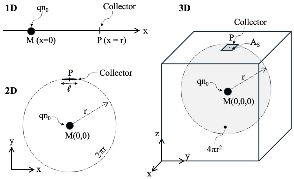
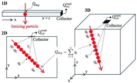
We first consider a point charge generated at at point M in a bulk semiconductor, and focus on the collection of this charge at point P () by a collector [35]. Figure 1 shows a schematic representation of this problem in 1D, 2D, and 3D. The distance between M and P is denoted by x in 1D and in 2D and 3D. The collector is reduced to a point in 1D; it corresponds to a small segment (length ) in 2D and to a small surface () in 3D. An excess carrier generated at the point source and transported at the level of the collector is considered to be collected upon its first passage through the collector.
Figure 1.
Schematics of the diffusion–collection problem in N = 1, 2, and 3 dimensions.
In the pure diffusion regime and in the presence of carrier recombination, the transport of the excess carrier density (expressed in the physical unit of ) in the semiconductor domain is governed by the following diffusion law [17,18,19]:
where is the carrier lifetime and D is the diffusion coefficient.
In the following, we examine the exact solution of Equation (1) in terms of excess carrier density, diffusion current, and collected charge (at the level of the collector contact) in the 1D, 2D, and 3D cases and in the presence or absence of carrier recombination. When possible, equations are first established for the general case of N dimensions (N = 1, 2, or 3).
3. Carrier Density and Diffusion Current
The excess carrier density at time t and distance r, originating from the initial charge , is the solution of Equation (1) and is given by [18]:
where N is the dimension of the problem (N = 1, 2, or 3) and is the N-dimensional Dirac delta function.
For electrons, the diffusion current density with the conventional direction of the electrical current is
Introducing Equation (2) into Equation (3) gives
where is the unit radial vector. The sign − indicates that, in the conventional current direction, the current flows toward the origin, even though the electrons diffuse outward on average.
To find the total current flowing through the collector, we integrate the radial component of over the whole collector surface inside the semiconductor, as explained and discussed in [35] for realistic collector structures integrated in front-end microelectronics. This effective collection surface in N dimensions is denoted and is equal to , and . Since the current density is constant on this surface,
Introducing the surface area of a hypersphere of radius r in N dimensions:
where is the ordinary gamma function [36], we can rewrite Equation (7) as follows:
In Equation (9), the first term corresponds to the initially generated point charge at the origin at , the second term is a pure geometrical term discussed below, and the third term is a time- and space-dependent function. corresponds to the collector’s solid angle, in N dimensions, viewed from the source, divided by the solid angle for the entire space, also in N dimensions. For , , for , and for , .
4. Maximum Times for Carrier Density and Current
The times at which and reach a maximum can be easily calculated from the time derivative of Equations (2) and (9), respectively. After straightforward calculations, we obtain the following:
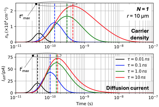
From Equations (10) and (11), for a given physical dimension N and carrier lifetime , we can establish that : the current systematically reaches its maximum slightly before the carrier density. This result is consistent with what was established in 3D without recombination [35]. This is because the current depends on the spatial derivative of the density, introducing an additional factor of 1/t, and altering the temporal balance between the power-law decay and the exponential decay. In other words, the current is proportional to the gradient of carrier density, which peaks before the density itself peaks.
In the absence of recombination, i.e., for large values of , Expressions (10) and (11) reduce to much simpler forms. Indeed, using the Taylor expansions, for small and for small leads to (see also Table 1):
Table 1.
Values of the times at which and reach their maxima as a function of the problem dimension (case without recombination).
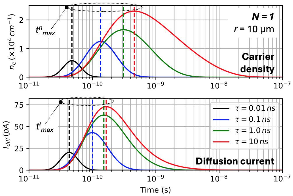
For N = 3, Equation (12) gives the expressions previously reported in [35]. Figure 2 shows the carrier density (Equation (2)) and the diffusion current (Equation (9)) as a function of time for several values of the carrier lifetime in dimension N = 1. The values of and , given by Equations (10) and (11), respectively, are also indicated, illustrating the time lead of the current over the carrier density, as previously discussed.
Figure 2.
Time evolution of the carrier density (Equation (2)) and the diffusion current (Equation (9)) for four different values of the carrier lifetime in dimension N = 1. Other simulation parameters are as follows: , , µm, D = 1000 cm2 s−1. The vertical dashed lines indicate the values of and , respectively, given by Equations (10) and (11).
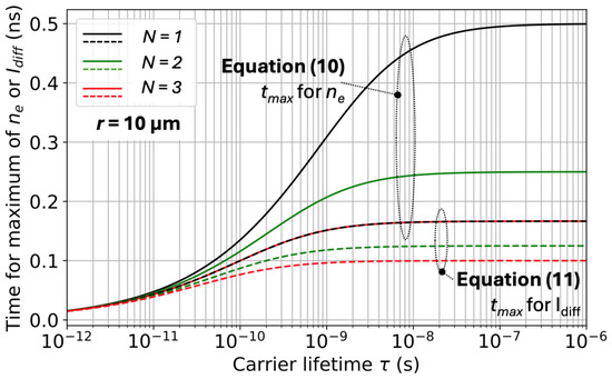
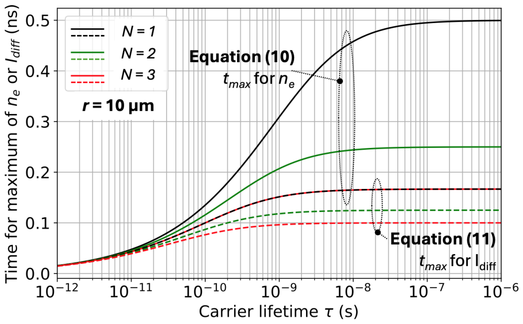
In addition, Figure 3 shows the evolution of and with the carrier lifetime , as a function of the dimension N. The time difference between the charge and current peaks is greatest when there is no recombination; it approaches zero as recombination increases, i.e., as the carrier lifetime decreases. This figure also highlights a result that is not evident when comparing Equations (10) and (11): for is equal to for .
Figure 3.
Evolution of and , respectively given by Equations (10) and (11), as a function of the carrier lifetime , for N = 1, 2, and 3. Simulation parameters are as follows: , µm, D = 1000 cm2 s−1.
5. Time Variations of the Collected Charge
The collected charge at point P can be evaluated from the time integral of the diffusion current:
with
This integral has no simple analytical closed-form due to the presence of the second term in the exponential function. However, it can be expressed exactly using , a special form of the incomplete modified Bessel function of the second kind [37,38,39], in the following form:
with
where , , and . is also called the “leaky aquifer integral” [37,38,39].
The final expression of the collected charge in N dimensions is then:
For , i.e., in the absence of recombination, the second argument of the function is zero, and the function reduces to the following:
where and is the upper incomplete gamma function [40,41]. This leads to the following expression of the collected charge without recombination:
We examine and discuss, in the following, these different expressions for N = 1, 2, and 3 with and without carrier recombination.
5.1. One-Dimensional Case ()
For , , and Equation (17) reduces to the following:
The function can be written in the following form (using Equation 7.4.33 from [42]):
where is the complementary error function [43,44].
Equation (20) gives with and :
In the absence of carrier recombination, i.e., when , and , we obtain the compact form:
5.2. Two-Dimensional Case ()
For and , Equation (17) can be rewritten as follows:
where cannot be reduced to a simple combination of erf or erfc functions. Nevertheless, in the absence of recombination, and a more compact form can be obtained:
5.3. Three-Dimensional Case ()
Finally, for and , Equation (17) gives the following:
For , i.e., without recombination, the second argument of the function is zero, and this quantity reduces to the following:
with , which leads to the same expression of the collected charge without recombination as already established in Ref. [35]:
Note that this incomplete gamma function takes the following special form [40]:
Equation (29) without recombination can be rewritten as follows:
6. Integral Collected Charge
The integral collected charge at point P corresponds to the charge collected over the time interval from zero to infinity:
where
This gives the following:
where is the modified Bessel function of the second kind (also called the Macdonald function) given by the integral form [37]:
6.1. Uni-Dimensional Case (N = 1)
For , we have the following [42,45]:
which gives
that immediately gives
When , , and the integral charge without recombination is equal to the following:
It is evident that the same expressions as in Equations (41) and (42) can be obtained when considering the limits of Equations (22) and (23), respectively, as t approaches infinity.
6.2. Bi-Dimensional Case (N = 2)
Similarly, for N = 2:
and the collected charge is therefore,
When , and , so in the absence of recombination:
6.3. Three-Dimensional Case (N = 3)
Now for , we have [42]:
Then,
and therefore
For , the case without recombination is immediate:
6.4. Alternative Formulation and Expression
A more general formulation of as a function of N can be directly obtained by inserting Equation (37) in Equation (35). After simplification, we obtain the following:
Using the surface area of the hypersphere given in Equation (8), the integral collected charge can also be expressed as follows:
From this equation, we can verify that
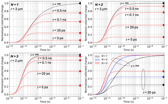
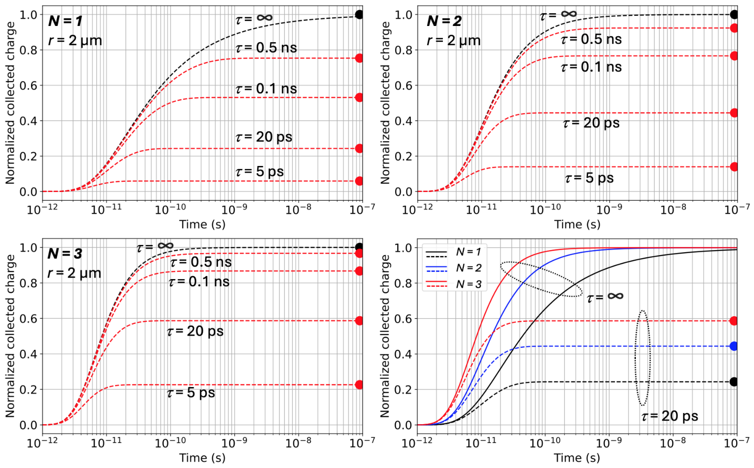
Figure 4 shows the time evolution of given by Equation (17) for different carrier lifetimes and for , , and , with a source–collector distance of r = 2 µm. As expected and for any dimension N, the collected charge increases over time and as the carrier lifetime increases, reaching a maximum when (red dots). The absolute maximum of the collected charge is obtained in all dimensions for when . These maximum values are respectively given by Equations (51) and (52), in the presence or absence of carrier recombination, respectively.
Figure 4.
Time evolution of given by Equation (17) for different values of the carrier lifetime for dimensions N = 1, 2, and 3 (dashed lines). The maximum values of the curves for in the presence of carrier recombination are given by Equation (51) (red dots), whereas the maximum values of the curve without recombination ( and ) are given by Equation (52) (black dots). The simulation parameters are as follows: r = 2 µm, D = 1000 cm2 s−1.
Finally, Figure 4 illustrates how the dimensionality of the diffusion problem influences the time dynamics of charge collection and the asymptotic collected fraction, with or without carrier recombination. On the one hand, the comparison between the curves should be interpreted as an indication of the role of dimensionality in the collection process, rather than as an absolute comparison between devices. Indeed, the cases , , and correspond to collection geometries defined in different spatial dimensions, with intrinsically different collector surfaces. As a result, the absolute value of the collected charge cannot be directly compared across dimensions without specifying an additional geometrical normalization. The curves mainly show that dimensionality modifies the rise time and the limiting collected fraction through the dimensional dependence of the diffusive flux toward the collector. On the other hand, the time dynamics of the collected charge result from the competition between diffusion and recombination. Initially, the collection is low because the carriers have not yet reached the collector. It then increases over a characteristic diffusion time , and finally reaches a plateau. In the absence of recombination (), all of the initial charge is ultimately collected, independently of N, because recombination losses are absent. Conversely, for a finite carrier lifetime, the plateau is lower than one and depends strongly on the dimension: in higher-dimensional idealized geometries, a larger fraction of the carriers can contribute to the flux through the effective collector before recombining. Thus, within the assumptions of the model, the 3D formulation leads to faster and more efficient collection than the corresponding 2D and 1D idealized cases.
7. Collection Efficiency and Recombination Factor
The collection efficiency of the collector is defined as the ratio of the charge actually collected at point P when to the charge initially generated by the particle at point M:
The recombination factor can be interpreted as a survival factor for carriers undergoing recombination. corresponds to negligible recombination (), while means that some carriers that could have reached P in the absence of recombination did not because they recombined along their diffusion path.
Considering developments and simplifications for N = 1, 2, and 3, we have the following:
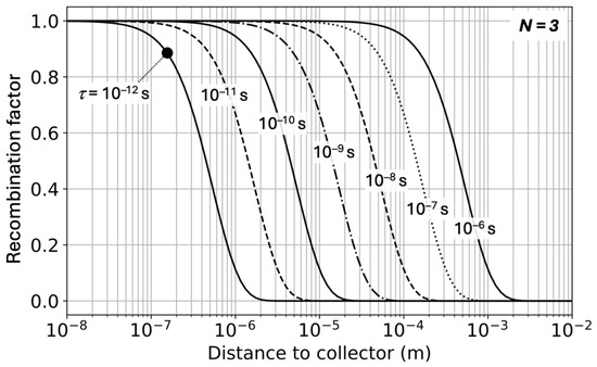
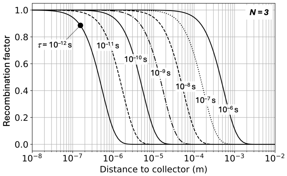
Figure 5 shows the evolution of the recombination factor as a function of r for different values of the carrier lifetime in dimension . This figure illustrates how the recombination factor decreases sharply with distance from the collector and how it depends on the lifetime . For small values of r, almost all of the charge is collected; however, beyond a critical distance that corresponds to the diffusion length, , most of the charge is lost through recombination. This distance increases with and follows , reflecting the competition between diffusion and recombination.
Figure 5.
Evolution of the factor of recombination as a function of r for different values of the carrier lifetime in dimension . Simulation parameters are as follows: , D = 1000 cm2 s−1.
8. Model Synthesis and Numerical Verification
This section summarizes all the equations of the proposed diffusion–collection model in three reference tables. Table 2 contains the most general equations, which can be used for any of the considered dimensions (N = 1, 2, or 3) and with recombination. It also lists the names and entry parameters of the corresponding functions given in Appendix A for implementing the model in Python (version 3.12.7). The general expressions for collected charge, integral collected charge, and collection efficiency use special functions, or Bessel integrals, that can be expressed using standard functions in certain cases. Table 3 and Table 4 present these equations in one, two, and three dimensions, with and without recombination, respectively. These tables provide simplified expressions for certain quantities.
Table 2.
Summary of the main general equations in N-dimensional diffusion–collection model with recombination. The names and input parameters of the corresponding Python functions described in Appendix A are also indicated.
Table 3.
Synthesis of the main equations in 1D, 2D, and 3D for the diffusion–collection model with recombination.
Table 4.
Synthesis of the main equations in 1D, 2D, and 3D for the diffusion–collection model without recombination.
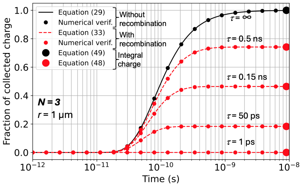
All of the model’s equations are analytical and correspond to exact solutions derived from the initial diffusion equation (Equation (1)) and its solution in terms of excess charge density (Equation (2)). However, we also checked all the equations numerically, starting from the numerical solution of Equation (1) with the initial condition given in Section 3. We solved this equation using a finite-difference discretization in space and an implicit backward Euler scheme in time [46]. We approximated the diffusion term using centered finite differences on a uniform, one-dimensional grid. We used a geometrically spaced time grid to capture transient and long-time dynamics [46].
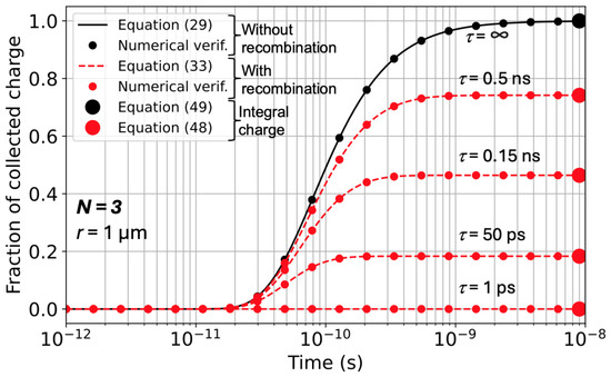
Figure 6 illustrates a typical comparison of analytical and numerical results for the time evolution of charge collected at a specific distance from a point charge, both with and without carrier recombination. As expected, these results highlight the validation of Equations (29), (33), (48), and (49) in three dimensions.
Figure 6.
Time evolution of the charge collected at a distance r from a point charge in the absence or presence of recombination in silicon. Results are normalized with respect to the integral charge given by Equation (49) without recombination. Simulation parameters are as follows: , r = 1 µm, D = 20 cm2 s−1. Analytical results (full and dotted lines) are also compared with numerical simulation (dot symbols).
9. Discussion
In this section, we discuss and demonstrate how to use the above equations to perform realistic single-event simulations and link them to the soft error rate of a given device. We will also address the question of generalizing our model.
9.1. Realistic Single-Event Simulations and Link with the SER
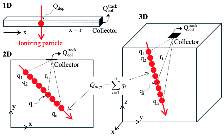
When a charged particle enters a semiconductor material, it gradually loses its kinetic energy as it penetrates deeper into the material, until it comes to a stop or exits the area of interest within the component or circuit [2]. The diffusion–collection model involves the conversion of energy lost by the particle into electron–hole pairs. These pairs are then rearranged into a succession of point charge densities of electrons and holes, also referred to as “charge packets”, as illustrated in Figure 7 [6]. This process occurs immediately after the energy deposition and the creation of the pairs, at the initial time . The model then operates under the assumption that the transport of the charge generated by the particle along its trajectory can be regarded as a superposition of independent transport processes for all point charge packets. In practice, only one type of carrier is considered for transport, i.e., electrons or holes, even though it is ambipolar in nature. This is because the collector collects either electrons or holes, depending on its type and/or the local bias state. Thus, the transport of each charge packet reduces to the problem addressed in this paper: the diffusion of a point charge in space and time with or without recombination.
Figure 7.
Schematics of charge creation by an ionizing particle along its path in 1D, 2D, and 3D. The total charge produced by the particle as it moves through the domain is broken down into a series of point charges. In the diffusion–collection approach, the transport of each point charge, along with the resulting current and charge collection, is considered to be an independent process.
Figure 7 illustrates this key point of the diffusion–collection approach: the transformation of continuous charge along the particle track into discrete charges for subsequent transport and collection using equations developed in the model. Note that in 1D, this transformation is reduced to a single point charge at the intersection of the semiconductor domain and the particle path. In two and three dimensions, the total charge generated by the particle in the domain of interest is divided into a series of point charges, , located at distances from the collector:
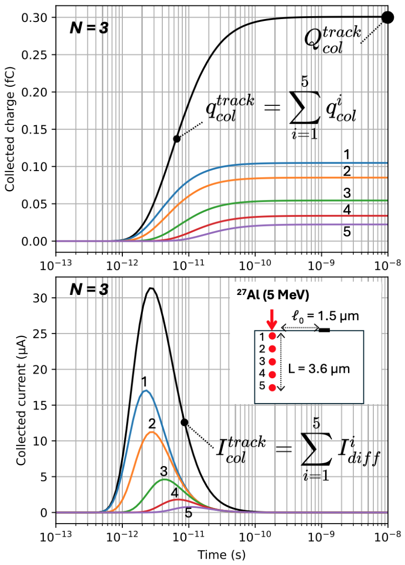
Each point charge, , independently diffuses and recombines in the semiconductor, contributing , , and , respectively, to the collected current, the collected charge, and the integral collected charge at the collector level. Thus, the total collected current, charge, and integral charge due to the complete particle track can be obtained by summing these contributions:
It is important to note at this point that the diffusion–collection model is based on a linear transport approximation. In this approximation, the carriers generated by the ionizing particle diffuse and recombine independently. This assumption corresponds to a linear, low-injection regime that is valid as long as the generated charge density is low enough that it does not perturb the local electric field or the transport and recombination parameters. Therefore, the model does not include collective effects, such as plasma effects, field screening, nonlinear recombination, or circuit-level feedback. These simplifications define the model range of validity.
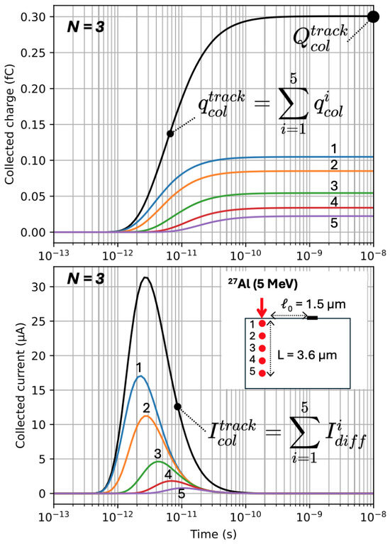
Figure 8 provides a numerical example in 3D of the collected current and the charge induced by the passage of a heavy ion close to a sensitive node in a silicon circuit. In this example (see the inset in Figure 8), a 5 MeV Al-27 heavy ion is incident normally on the silicon surface at a distance = 1.5 µm from the collector and comes to rest after 3.6 µm in the Si volume (as given by SRIM [47,48]). The particle LET is about 10 MeV cm2 mg−1 [47,48] and the ion generates a total charge pC along its track. For simplicity and clarity, this charge is divided into only five point charges that are regularly spaced along the particle path. Figure 8 shows the five individual contributions to the total collected quantities, and , as well as the resulting time profiles of these global quantities, obtained by summation. In practice, values of n ranging from 20 to 100, as a function of track length, provide satisfactory numerical accuracy. In the case of multiple secondary particles, as encountered in neutron interactions with target material atoms, the generated charge is decomposed/discretized on different particle tracks. Then, the summation in Equation (59) is applied to the total number of charge packets associated with all secondary ionizing particles.
Figure 8.
Example showing how to compute in 3D the collected current and the collected charge induced by the passage of a heavy ion near a sensitive node in a silicon circuit. A 5 MeV Al-27 ion arrives perpendicularly to the silicon surface at the distance = 1.5 µm from the collector and stops at L = 3.6 µm within the Si volume. The ion track is decomposed into five charge packets regularly spaced along the particle track. The other simulation parameters are as follows: m2, D = 1000 cm2 s−1, s, = 10 MeV cm2 mg−1.
Computing the collected charges due to a set of incoming ionizing particles or nuclear reactions in a semiconductor domain that accounts for the geometry of a given device or circuit (possibly including multiple sensitive nodes or collectors) makes it possible to identify and count all events that induce a collected charge greater than the critical charge, :
where is the minimum charge required to cause a circuit to malfunction due to a particle strike [2]. This enables a direct estimation of the soft error rate of the considered device or circuit. This topic is beyond the scope of this study. However, the development of a code for estimating the soft error rate is essentially based on the equations presented in this paper. The other aspects of the code are limited to reading an event database, generating clusters of charge packets, performing various geometric calculations—including the distances between point charges and the circuit’s collector(s)—and applying criteria for detecting logic errors.
9.2. Generalization of the Model
The generalization of the proposed diffusion–collection model must be understood in relation to its underlying assumptions. The model is formulated for an idealized semiconductor medium with effective transport parameters, such as diffusion coefficient and carrier lifetime, and simplified collection geometries. Consequently, the model applies to situations in which charge transport is diffusion-dominated, recombination can be represented by an effective lifetime, and the collection region can be approximated as planar, cylindrical, or spherical. These situations include weak-field regions, undepleted substrates, epitaxial layers, and regions located far enough from high-field junctions that diffusion remains the main mechanism controlling the delayed component of the charge collection. The same mathematical framework can be used for different semiconductor materials, provided that the relevant material parameters are adapted. In particular, the diffusion coefficient, mobility, carrier lifetime, ionization energy, recombination properties, and effective collection length must be chosen consistently with the material under consideration. While the model is not restricted to silicon in its mathematical form, its quantitative predictions depend on the availability and accuracy of these material-dependent parameters. This is especially important for wide-bandgap or oxide semiconductors, as carrier mobility, trapping, defect-assisted recombination, and radiation-induced changes in material properties may differ significantly from conventional silicon technologies.
The applicability of the model to realistic semiconductor devices depends on the device architecture and biasing conditions. In modern CMOS devices, FinFETs, fully depleted structures, oxide semiconductor transistors, and neuromorphic devices, the electric field distribution, doping profile, interfaces, contacts, and boundary conditions may be highly nonuniform. In such cases, the present analytical model should not be viewed as a replacement for full device simulations. Instead, it offers a simplified description that captures the diffusion–recombination aspect of charge transport. This description can be used to interpret numerical simulations, estimate collection times, evaluate limiting cases, and provide compact input parameters for higher-level soft-error-rate models.
The main limitation of the current formulation is its inability to explicitly resolve complex, three-dimensional device geometries; nonuniform electric fields; field-enhanced drift; carrier trapping at interfaces; nonlinear recombination; and time-dependent material degradation under irradiation. When these effects dominate the transient response, TCAD or multi-physics numerical simulations are still necessary. Nevertheless, the analytical framework is useful as a reference model because it identifies the dependencies of collected charge on distance, dimensionality, diffusion coefficient, carrier lifetime, and collection geometry. The framework’s strength lies not in providing an exact description of every device configuration, but rather in its ability to offer a transparent baseline for diffusion-driven charge collection across various materials and device structures.
10. Conclusions
In conclusion, this paper presents a unified analytical framework for modeling charge diffusion and collection in semiconductor materials. This framework is valid in one, two, and three dimensions and includes carrier recombination. Starting from the diffusion equation for an initial point charge, we derived analytical expressions for the carrier density, diffusion current, and collected charge as functions of time and distance.
The proposed model emphasizes the role of geometry through dimension-dependent factors, providing a consistent description of the diffusion–collection process across different configurations. The use of special functions allows for an exact treatment of recombination effects while maintaining analytical compactness. The analysis also reveals important physical characteristics, such as the temporal shift between the maxima of the current and carrier density and the effect of recombination on collection efficiency.
Beyond its theoretical value, this framework is a practical building block for modeling and simulating radiation-induced transient effects and the soft error rate (SER) in semiconductor devices. Its compact formulation and straightforward implementation make it well-suited for integration into reliability-oriented simulation tools. Future extensions may include electric field effects and more complex device geometries.
Author Contributions
Conceptualization, J.-L.A. and D.M.; methodology, A.A., D.M. and J.-L.A.; software, A.A., J.-L.A. and D.M.; formal analysis, A.A., D.M. and J.-L.A.; investigation, J.-L.A., D.M. and A.A.; writing—review and editing, J.-L.A., D.M. and A.A.; visualization, A.A., D.M. and J.-L.A. All authors have read and agreed to the published version of the manuscript.
Funding
This research received no external funding.
Institutional Review Board Statement
Not applicable.
Informed Consent Statement
Not applicable.
Data Availability Statement
The original contributions presented in this study are included in the article. Further inquiries can be directed to the corresponding author.
Conflicts of Interest
The authors declare no conflicts of interest.
Appendix A. Model Implementation in Python
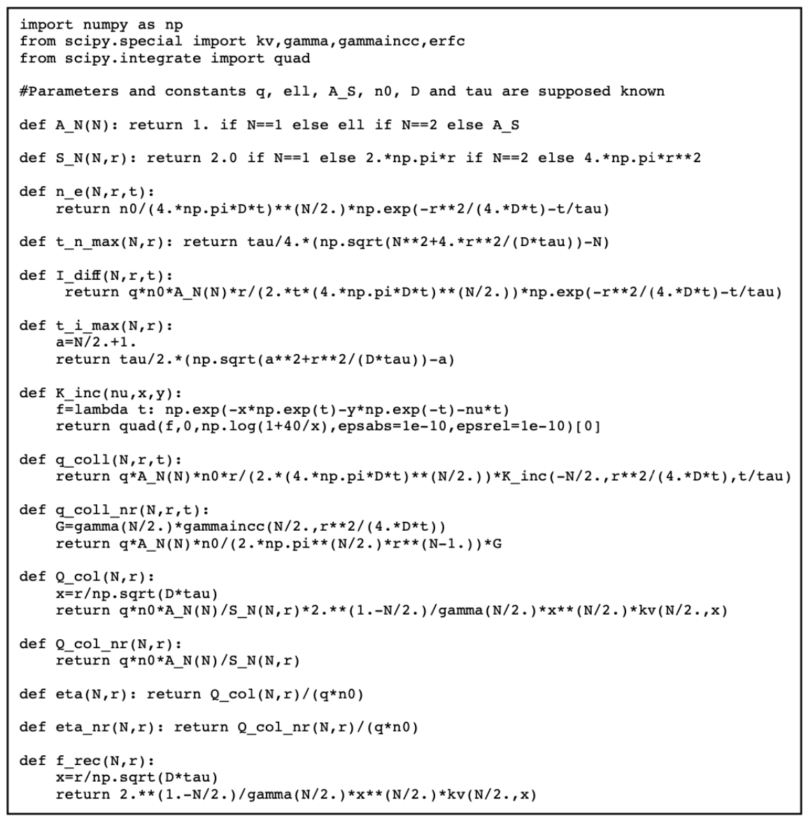
The following code (Figure A1) provides a minimal implementation of the main equations of the model in Python [49]. We assume that parameters and constants q, ℓ, , , D, and have been declared and assigned numerical values.
Note that the integral , defined in Equation (16), is numerically evaluated here (function K_inc(nu,x,y)). In practice, and from a numerical perspective, a better integration variable for Equation (16) is , which gives:
This form is much more stable for direct numerical integration. Since the integrand decays as as , we can truncate it to a maximum value of about , where A is a real number with a typical value of .
Alternatively, analytical expressions for and for can be used, namely Equations (21) and (32), for dimensions N = 1 and N = 3.
References
- Leroy, C.; Rancoita, P.G. Principles of Radiation Interaction Matter and Detection; World Scientific Publishing Co. Pte. Ltd.: Singapore, 2004. [Google Scholar]
- Autran, J.-L.; Munteanu, D. Soft Errors: From Particles to Physics; Taylor & Francis/CRC Press: Boca Raton, FL, USA, 2015. [Google Scholar]
- Murat, M.; Akkerman, A.; Barak, J. Electron and Ion Tracks in Silicon: Spatial and Temporal Evolution. IEEE Trans. Nucl. Sci. 2008, 55, 3046–3054. [Google Scholar] [CrossRef] [Scilit]
- Dood, P.E.; Massengill, L.W. Basic Mechanisms and Modeling of Single-Event Upset in Digital Microelectronics. IEEE Trans. Nucl. Sci. 2003, 50, 583–602. [Google Scholar] [CrossRef] [Scilit]
- Munteanu, D.; Autran, J.L. Modeling and Simulation of Single-Event Effects in Digital Devices and ICs. IEEE Trans. Nucl. Sci. 2008, 55, 1854–1878. [Google Scholar] [CrossRef] [Scilit]
- Autran, J.L.; Munteanu, D. Multiscale, Multiphysics Modeling and Simulation of Single-Event Effects in Digital Electronics: From Particles to Systems. IEEE Trans. Nucl. Sci. 2024, 71, 31–66. [Google Scholar] [CrossRef] [Scilit]
- Ziegler, J.F.; Puchner, H. SER—History, Trends and Challenges; Cypress Semiconductor: San Jose, CA, USA, 2004. [Google Scholar]
- Fleetwood, D.M. Radiation Effects in a Post-Moore World. IEEE Trans. Electron Devices 2021, 68, 509–545. [Google Scholar] [CrossRef] [Scilit]
- Messenger, G.C.; Ash, M.S. Single Event Phenomena; Springer: Dordrecht, The Netherlands, 1997. [Google Scholar]
- Qu, S.; Yu, Q.; Jiang, C.; Zou, T.; Xu, H.; Zhang, L.; Tao, M.; Zhu, Q.; Zhang, S.; Geng, C.; et al. Oxide Semiconductor in a Neuromorphic Chromaticity Communication Loop for Extreme Environment Exploration. Sci. Adv. 2025, 11, eadu3576. [Google Scholar] [CrossRef] [Scilit] [PubMed]
- Oh, S.; Kim, H.; Oh, J.; Kim, H.; Kim, S.; Cho, H.-S.; Kim, C. Enhancing Proton Irradiation Tolerance of a-IGZO Thin-Film Transistors through Hydrogen Doping. J. Mater. Chem. C 2026, 14, 3637–3647. [Google Scholar] [CrossRef] [Scilit]
- Synopsys, TCAD. Available online: https://www.synopsys.com/silicon/tcad.html (accessed on 25 May 2026).
- Silvaco, Semiconductor Process and Device Simulation. Available online: https://silvaco.com/tcad/ (accessed on 25 May 2026).
- Cogenda, Large-Scale Semiconductor Devices Simulation. Available online: https://www.cogenda.com/ (accessed on 25 May 2026).
- COMSOL Multiphysics (Documentation). Available online: https://www.comsol.com/ (accessed on 20 May 2026).
- Munteanu, D.; Autran, J.L.; Ferlet-Cavrois, V.; Paillet, P.; Baggio, J.; Castellani, K. 3D Quantum Numerical Simulation of Single-Event Transients in Multiple-Gate Nanowire MOSFETs. IEEE Trans. Nucl. Sci. 2007, 54, 994–1001. [Google Scholar] [CrossRef] [Scilit]
- Kirkpatrick, S. Modeling Diffusion and Collection of Charge from Ionizing Radiation in Silicon Devices. IEEE Trans. Electron Devices 1979, 26, 1742–1753. [Google Scholar] [CrossRef] [Scilit]
- Messenger, G.C. Collection of Charge on Junction Nodes from Ion Tracks. IEEE Trans. Nucl. Sci. 1982, 29, 2024–2031. [Google Scholar] [CrossRef] [Scilit]
- Edmonds, L.D. Charge Collected by Diffusion from an Ion Track under Mixed Boundary Conditions. IEEE Trans. Nucl. Sci. 1991, 38, 834–837. [Google Scholar] [CrossRef] [Scilit]
- Wouters, S. Diffusion-Based Silicon Radiation Detectors; Delft University Press: Delft, The Netherlands, 1992. [Google Scholar]
- Smith, E.C.; Stassinopoulos, E.G.; LaBel, K.; Brucker, G.; Seidlick, C.M. Application of a diffusion model to SEE cross sections of modern devices [DRAMs]. IEEE Trans. Nucl. Sci. 1995, 42, 1772–1779. [Google Scholar] [CrossRef] [Scilit]
- Edmonds, L.D. SEU Cross Sections Derived from a Diffusion Analysis. IEEE Trans. Nucl. Sci. 1996, 43, 3207–3217. [Google Scholar] [CrossRef]
- Palau, J.M.; Hubert, G.; Coulie, K.; Sagnes, B.; Calvet, M.C.; Fourtine, S. Device Simulation Study of the SEU Sensitivity of SRAMs to Internal Ion Tracks Generated by Nuclear Reactions. IEEE Trans. Nucl. Sci. 2001, 48, 225–231. [Google Scholar]
- Palau, J.M.; Wrobel, R.; Castellani-Coulie, K.; Calvet, M.C.; Dodd, P.E.; Sexton, F.W. Monte Carlo Exploration of Neutron-Induced SEU-Sensitive Volumes in SRAMs. IEEE Trans. Nucl. Sci. 2002, 49, 3075–3081. [Google Scholar] [CrossRef]
- Lambert, D.; Baggio, J.; Ferlet-Cavrois, V.; Flament, O.; Saigne, F.; Sagnes, B.; Buard, N.; Carriere, T. Neutron-Induced SEU in Bulk SRAMs in Terrestrial Environment: Simulations and Experiments. IEEE Trans. Nucl. Sci. 2004, 51, 3435–3441. [Google Scholar] [CrossRef] [Scilit]
- Merelle, T.; Chabane, H.; Palau, J.M.; Castellani-Coulie, K.; Wrobel, F.; Saigne, F.; Sagnes, B.; Boch, J.; Vaille, J.R.; Gasiot, G.; et al. Criterion for SEU Occurrence in SRAM Deduced from Circuit and Device Simulations in Case of Neutron-Induced SER. IEEE Trans. Nucl. Sci. 2005, 52, 1148–1155. [Google Scholar] [CrossRef] [Scilit]
- Wrobel, F.; Hubert, G.; Iacconi, P. A Semi-Empirical Approach for Heavy Ion SEU Cross Section Calculations. IEEE Trans. Nucl. Sci. 2006, 53, 3271–3276. [Google Scholar] [CrossRef] [Scilit]
- Correas, V.; Saigne, F.; Sagnes, B.; Boch, J.; Gasiot, G.; Giot, D.; Roche, P. Innovative Simulations of Heavy Ion Cross Sections in 130 nm CMOS SRAM. IEEE Trans. Nucl. Sci. 2007, 54, 2413–2418. [Google Scholar] [CrossRef] [Scilit]
- Correas, V.; Saigne, F.; Sagnes, B.; Boch, J.; Gasiot, G.; Giot, D.; Roche, P. Simulation Tool for the Prediction of Heavy Ion Cross Section of Innovative 130-nm SRAMs. IEEE Trans. Nucl. Sci. 2008, 55, 2036–2041. [Google Scholar] [CrossRef] [Scilit]
- Artola, L.; Hubert, G.; Duzellier, S.; Bezerra, F. Collected Charge Analysis for a New Transient Model by TCAD Simulation in 90 nm Technology. IEEE Trans. Nucl. Sci. 2010, 57, 1869–1875. [Google Scholar] [CrossRef] [Scilit]
- Artola, L.; Hubert, G.; Warren, K.M.; Gaillardin, M.; Schrimpf, R.D.; Reed, R.A.; Weller, R.A.; Ahlbin, J.R.; Paillet, P.; Raine, M.; et al. SEU Prediction From SET Modeling Using Multi-Node Collection in Bulk Transistors and SRAMs Down to the 65 nm Technology Node. IEEE Trans. Nucl. Sci. 2011, 58, 1338–1346. [Google Scholar] [CrossRef] [Scilit]
- Edmonds, L.D. A Theoretical Analysis of the Role of Ambipolar Diffusion in Charge-Carrier Transport in a Quasi-Neutral Region Under High Injection. IEEE Trans. Nucl. Sci. 2011, 58, 2459–2469. [Google Scholar] [CrossRef] [Scilit]
- Martinie, S.; Autran, J.L.; Sauze, S.; Munteanu, D.; Uznanski, S.; Roche, P.; Gasiot, G. Underground Experiment and Modeling of Alpha Emitters Induced Soft-Error Rate in CMOS 65 nm SRAM. IEEE Trans. Nucl. Sci. 2012, 59, 1048–1053. [Google Scholar] [CrossRef] [Scilit]
- Autran, J.L.; Munteanu, D. Physics-Based Analytical Formulation of the Soft Error Rate in CMOS Circuits. IEEE Trans. Nucl. Sci. 2023, 70, 782–791. [Google Scholar] [CrossRef] [Scilit]
- Autran, J.L.; Munteanu, D. New Insights into Diffusion–Collection Modeling of Radiation-Induced Charge in Semiconductor Devices. J. Appl. Phys. 2023, 134, 175701. [Google Scholar] [CrossRef] [Scilit]
- Askey, R.A.; Roy, R. Gamma Function. In NIST Handbook of Mathematical Functions; Cambridge University Press: Cambridge, UK, 2010; Chapter 5. [Google Scholar]
- Harris, F.E. Incomplete Bessel, generalized incomplete gamma, or leaky aquifer functions. J. Comput. Appl. Math. 2008, 215, 260–269. [Google Scholar] [CrossRef] [Scilit]
- Alford, J.A. Calculation of the generalized leaky aquifer integral. Comput. Phys. Commun. 2005, 173, 1–8. [Google Scholar] [CrossRef] [Scilit]
- Temme, N.M. The leaky aquifer function revisited. Int. J. Quantum Chem. 2009, 109, 2826–2830. [Google Scholar] [CrossRef] [Scilit]
- Paris, R.B. Incomplete Gamma and Related Functions. In NIST Handbook of Mathematical Functions; Cambridge University Press: Cambridge, UK, 2010; Chapter 8. [Google Scholar]
- Chaudhry, M.A.; Zubair, S.M. Generalized incomplete gamma functions with applications. J. Comput. Appl. Math. 1994, 55, 99–124. [Google Scholar] [CrossRef] [Scilit]
- Abramowitz, M.; Stegun, I.E. Handbook of Mathematical Functions with Formulas, Graphs, and Mathematical Tables; National Bureau of Standards Applied Mathematics: Gaithersburg, MD, USA, 1972; Series 55. [Google Scholar]
- Lebedev, N.N. Special Functions and Their Applications; Prentice Hall: Englewood Cliffs, NJ, USA, 1965. [Google Scholar]
- Temme, N.M. Error Functions, Dawson’s and Fresnel Integrals. In NIST Handbook of Mathematical Functions; Cambridge University Press: Cambridge, UK, 2010; Chapter 7. [Google Scholar]
- Olver, F.W.J.; Maximon, L.C. Bessel functions. In NIST Handbook of Mathematical Functions; Cambridge University Press: Cambridge, UK, 2010; Chapter 10. [Google Scholar]
- LeVeque, R.J. Finite Difference Methods for Ordinary and Partial Differential Equations; Society for Industrial and Applied Mathematics: Philadelphia, PA, USA, 2007. [Google Scholar]
- Ziegler, J.F.; Ziegler, M.D.; Biersack, J.P. SRIM—The stopping and range of ions in matter. Nucl. Instrum. Meth. B 2010, 268, 1818–1823. [Google Scholar] [CrossRef] [Scilit]
- SRIM. Available online: http://srim.org (accessed on 20 April 2026).
- NumPy. Available online: https://numpy.org/ (accessed on 15 April 2026).

Disclaimer/Publisher’s Note: The statements, opinions and data contained in all publications are solely those of the individual author(s) and contributor(s) and not of MDPI and/or the editor(s). MDPI and/or the editor(s) disclaim responsibility for any injury to people or property resulting from any ideas, methods, instructions or products referred to in the content. |
© 2026 by the authors. Licensee MDPI, Basel, Switzerland. This article is an open access article distributed under the terms and conditions of the Creative Commons Attribution (CC BY) license.