


Abstract
Optically transparent, broadband, angular-stable absorbers have emerged with much interests. In this paper, a broadband and wide-angle optically transparent metasurface (MS)-based absorber (MA) using indium-tin-oxide (ITO) deposited on polyethylene terephthalate (PET) is proposed. The proposed MA is composed of an on-top polydimethylsiloxane (PDMS), a middle MS-structure ITO-PET film, a bottom PDMS, and a bottom continuous ITO-PET film. An equivalent circuit model (ECM) is used to study the mechanism of wideband absorptivity in theory, the surface current distributions are displayed to study the physical insight of peak absorptivity, and parameter studies are given to verify the robustness of the proposed MA. Four electric and magnetic resonances are generated and combined to achieve wideband and high absorptivity. Over 90% absorptivity from 6.26 to 24.86 GHz with a fractional bandwidth of 119.54% is obtained under normal incidence. Moreover, over 85% absorptivity within the incident angle of 45° under TE and TM polarizations are obtained, respectively. The measured light transmittance is 66.95%, and the measured absorptivity under normal and oblique incidences is in good agreement with the simulations. The proposed design has the advantages of wideband and angular-stable absorptivity, good light transmittance, and a compact structure, which can find application for transparent stealth platforms and electromagnetic shielding.
1. Introduction
Absorbers, associating with the materials that can absorb the energy, have been widely used in radar cross section (RCS) reduction platforms and electromagnetic interference protection devices [1]. For example, by coating with absorbing materials, the scattered energy is absorbed to obtain RCS reduction platforms, such as aircraft, ship, etc. [2]. With the development of RCS reduction technologies, wideband and angular-stable absorption performance and low-profile structure have attracted more interest. Moreover, the absorbers are also required to be light transparent, such as the windows of the RCS reduction aircraft and ship.
Metasurfaces, as a type of planar two-dimensional metamaterial, have been widely used in controlling the magnitude, phase, and polarization of electromagnetic (EM) waves [3,4,5,6,7,8,9,10,11,12,13,14]. Due to their special characteristics, metasurface (MS)-based absorbers (MAs) have been proposed for EM wave absorption for microwave, millimeter wave, and THz wave [8,9,10]. Perfect absorption is obtained at a narrow band by using split-ring and wire resonators [15]. To broaden the absorption bandwidth, two methods have been proposed. The first one is by designing single-layered composite resonators [16,17,18]. For example, a wideband ultrathin MA by combing ring and patch resonators was tuned to realize above 90% absorptivity in the frequency range of 11.3–18.7 GHz [18]. The second one is by designing multi-layered structures [19,20,21]. In [22], a multilayer absorber with resistive film and checkerboard metasurfaces was proposed to absorb energy from 2.8 GHz to 18 GHz. However, these designs are obtained by using printed circuit board (PCB) technology and opaque substrates, and cannot be used for transparent applications.
Recently, some transparent MAs have been proposed by depositing transparent films on transparent substrates [23,24,25,26,27,28,29,30,31,32,33,34,35,36,37,38,39,40]. The transparent films are obtained by using several types of materials, including mesh lines [23,24], ink-based material [25], water-based material [26], indium-tin-oxide (ITO) [27,28,29,30,31,32], and hybrid materials [33,34]. Recently, thanks to the easy fabrication and low cost of ITO films, many ITO-based MA have been proposed [35,36,37,38,39,40,41]. For example, a single-layer ITO-based composite MS structure deposited on a transparent substrate is proposed for broadband absorption in [35]. In [37], the ITO is deposited on glass. The wideband absorption is obtained by using a hybrid structure of several pairs of arcs and a grid mesh ground, and the absorptivity is >70% and >90% at an incident angle of 60° for TE and TM polarizations, respectively. In [40], the wideband absorption is obtained by using three circular rings. The absorptivity is >70% and >90% at an incident angle of 60° for TE and TM polarizations, respectively. However, it is still challenging to obtain wideband, angular-stable, and low-profile MA.
In this paper, a broadband and angular-stable optically transparent MA based on ITO is proposed. The equivalent circuit model (ECM) analysis and surface currents distribution are utilized to study the physical insight of the mechanism. In addition, parameter studies are given to demonstrate the robustness of the proposed design. It is shown that the light transmittance is 66.95%, and over 90% absorptivity from 6.26 GHz to 24.86 GHz with a fractional bandwidth of 119.54% is obtained under normal incidence. Moreover, a good angular stability of the broadband and high absorptivity is obtained for oblique incidences.
2. Design and Mechanism
2.1. Schematic View, Performance and Design Process of the Unit
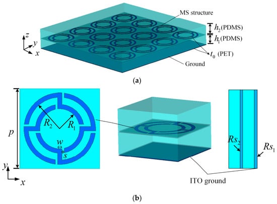
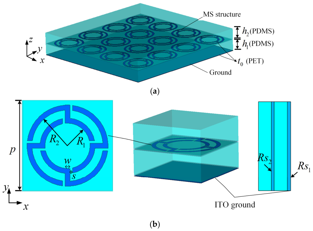
Figure 1a shows the three-dimensional (3D) schematic view of the proposed broadband and angular-stable MA. From top to bottom of the proposed MA, it consists of a transparent substrate PDMS with the thickness of h2, an MS-structure ITO-PET film, a transparent substrate PDMS with the thickness of h1, and a continuous ITO-PET film (full-covered ITO film). The thickness of the PET is t0 = 0.125 mm, and the thickness of the ITO is 170 nm. The details of the unit cell is shown in Figure 1b. The MS structure is composed of four mender lines. Both the two substrates made of PDMS have a relative permittivity of 2.25 and a loss tangent of 0.008. The MA was simulated and analyzed by using the commercial software Microwave Studio CST 2020. The ITO conductivity was on the order of 105 [42], the loss tangents of PDMS/PET are assumed as unchanged of 0.008/0.0071 at the target band [43], and they are carried out at room temperature. The geometry was optimized for wideband and angular-stable absorption, and the final parameters are p = 9, R1 = 2.25, R2 = 3.55, w = 0.5, s = 0.25, t0 = 0.125, h1 = 3, h2 = 3, and Rs1 = Rs2 = 10Ω/sq (unit: mm).
Figure 1.
Schematic view of the MA: (a) 3D view; (b) detailed middle view and side view.
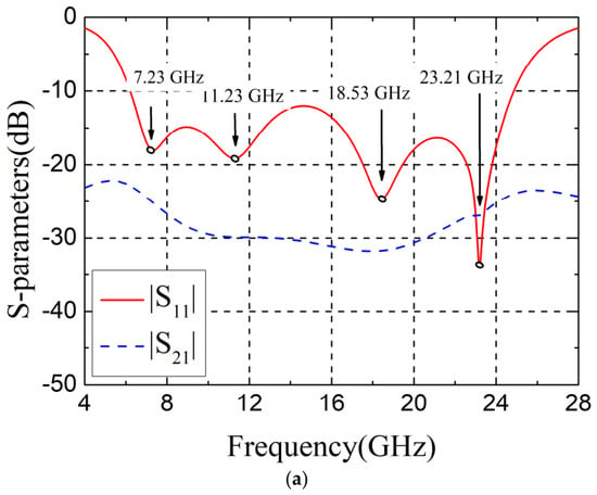
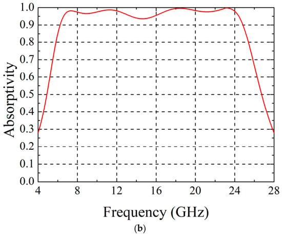
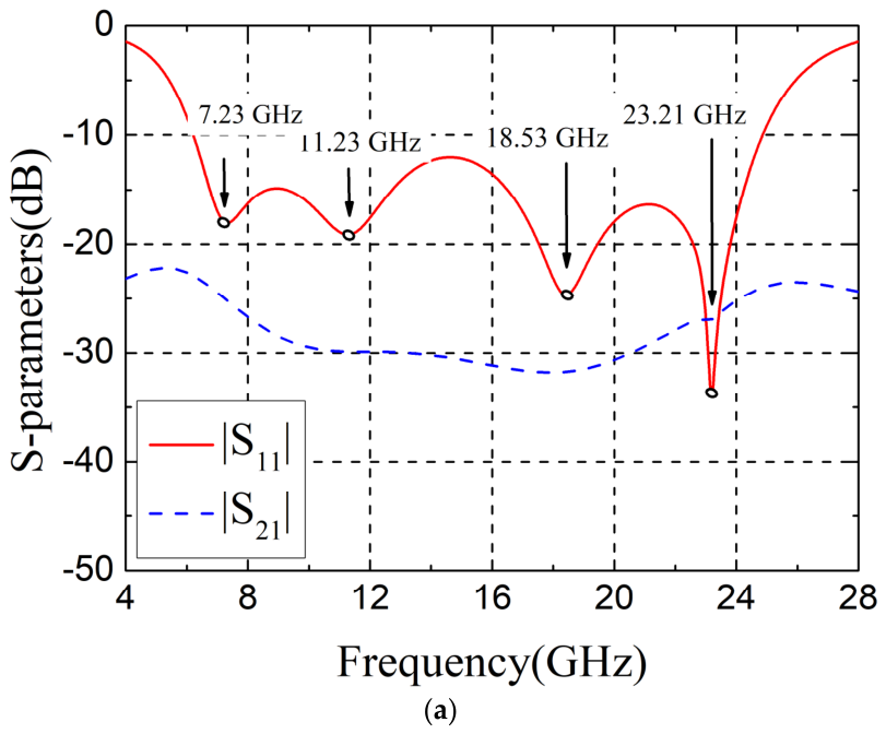
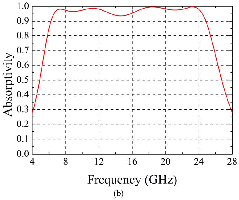
Figure 2a shows the S-parameters of the proposed MS under a y-polarized normally incident EM wave, where the |S11| represents the reflection coefficient and |S21| represents the transmission coefficient. It can be seen that the bandwidth of |S11| < −10 dB from 6.19 GHz to 24.94 GHz is obtained, and the |S21| is less than −20 dB within the bands. Four frequency resonances of 7.23 GHz, 11.23 GHz, 18.53 GHz, and 23.21 GHz are obtained. To evaluate the characteristic of absorption, the absorptivity defined as A = 1 − |S11|2 − |S21|2 is used. The calculated absorptivity is given in Figure 2b. Over 90% absorption is obtained from 6.26 GHz to 24.86 GHz with a fractional bandwidth (FBW) of 119.54% (FBW=2 × (fh−fl)/fh+fl) × 100%, where fl and fh is the lower and higher frequencies of the band, respectively), covering the X, Ku, and part of the Ka bands. The same results can be obtained for an x-polarized incident EM wave due to the symmetric geometry.
Figure 2.
Performance of the unit (a) S-parameters and (b) absorptivity.
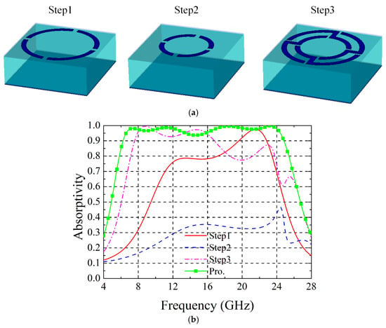
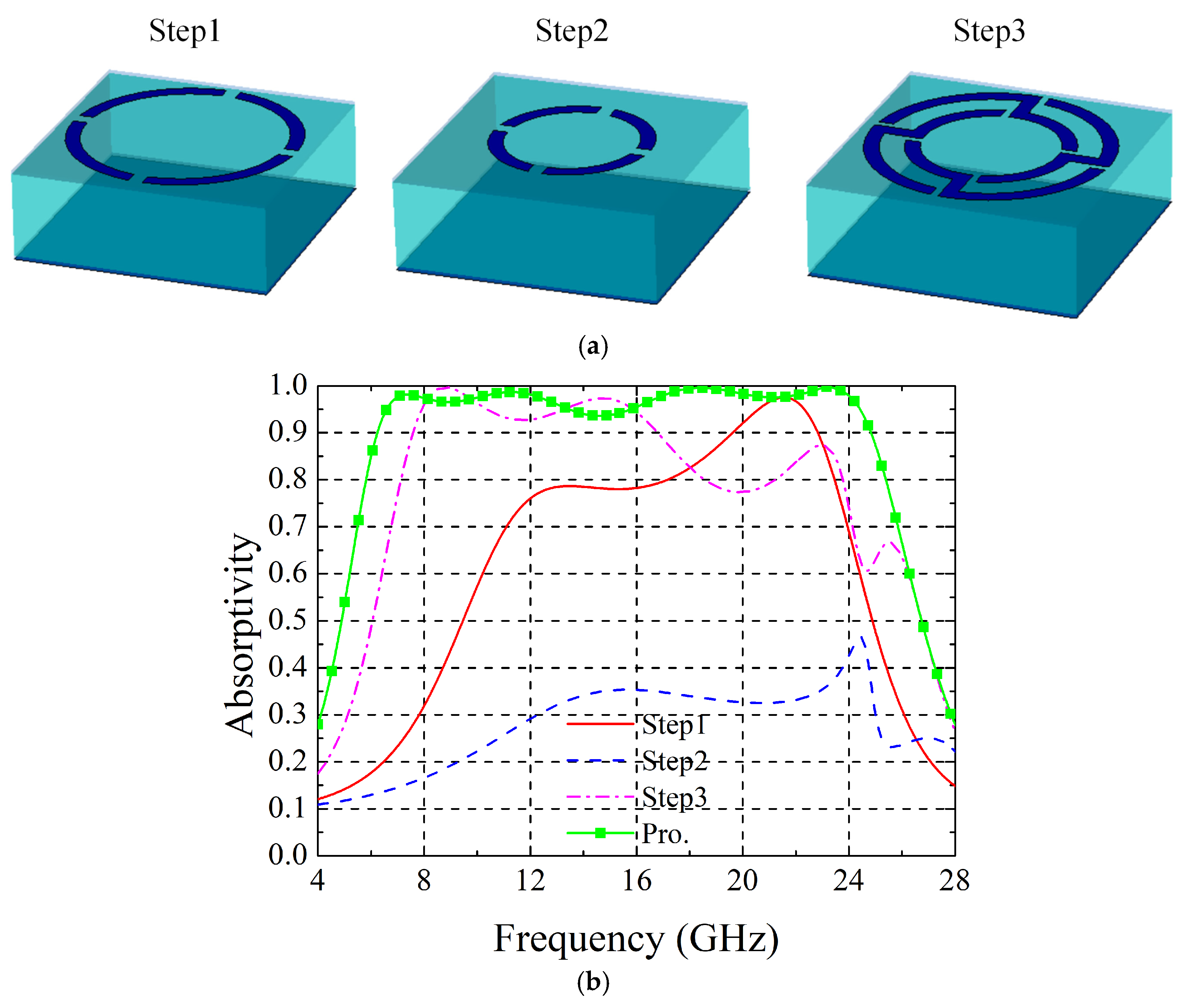
Figure 3 gives the design process of the proposed MA and the absorptivity of each step. In Step 1, a split ring with a radius of R1 is designed, and two resonances at 12.98 GHz and 21.57 GHz are generated. The peak values are 0.79 and 0.98, respectively. In Step 2, a split ring with a radius of R2 is designed, and two resonances at 15.21 GHz and 21.53 GHz are generated. The peak values are 0.36 and 0.47, respectively. In Step 3, by combining the two split rings at Step 1 and Step 2, four resonances at 8.82, 14.81, 22.96 and 25.52 GHz with the peak values of 1.00, 0.98, 0.87, and 0.67 are obtained, but the absorptivity at the high frequency region is less than 90%. The ring widths are kept the same as 0.5 mm for comparison. It is also noted that the lowest resonant frequency is shifted to 8.9 GHz, indicating a size miniaturization by the connection of the two rings in Step 3. By integrating a compensated layer made of PDMS with the thickness of h2, the proposed MA is obtained, and wideband and high absorptivity are ensured. Four frequency resonances of 7.23, 11.23, 18.53, and 23.21 GHz with the peak values of 1.00 are obtained.
Figure 3.
Design steps and performance: (a) design process; (b) absorptivity of each step.
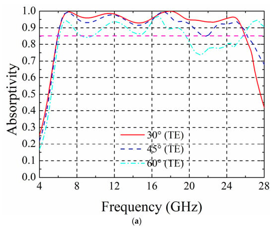
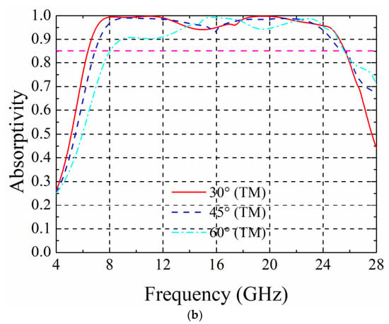
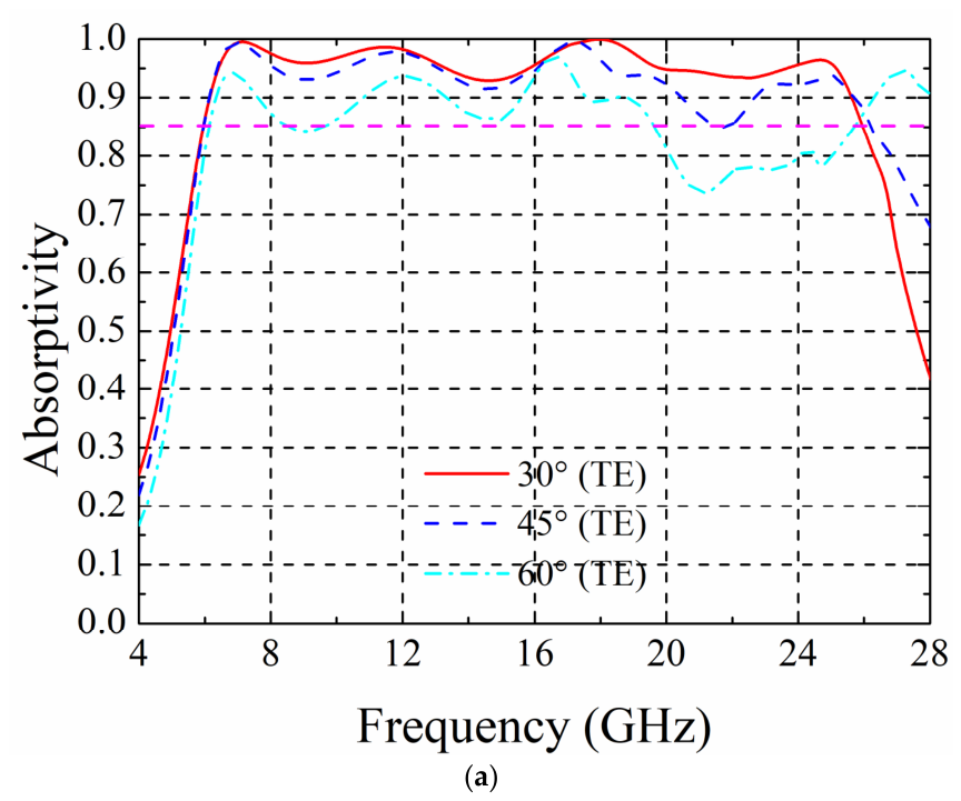
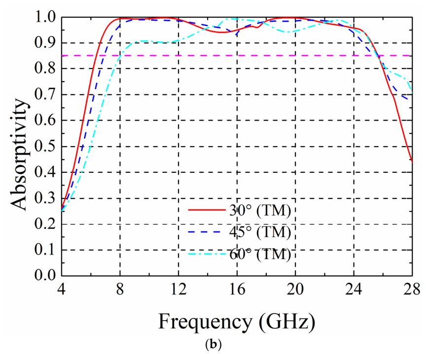
To study the absorption performance under oblique incident EM waves, the absorptivity under transverse electric (TE) and transverse magnetic (TM) polarizations are given in Figure 4. As shown in Figure 4a, the proposed MS achieves over 85% absorptivity within the incident angle of 45° under TE polarization, and achieves over 75% absorptivity with the incident angle of 60°. As shown in Figure 4b, the proposed MS achieves over 90% absorptivity within the incident angle of 60° under TM polarization. The surface impedances for TE/TM polarization are written as and , respectively. When the incident angle increases, the impedances of the TE and TM are deviated with the free space impedance, and the impedance is inversely proportional/ proportional to cosθ, respectively, indicating a decreased operating band and efficiency.
Figure 4.
Simulated absorption under oblique incidence: (a) TE polarization; (b) TM polarization.
2.2. Mechanism and Theoretical Analysis
To study the physical insight of the proposed MA, the equivalent circuit model (ECM) is used to study the mechanism of wideband and wide-angle absorption from the perspective of resistive film properties. Then the surface current distributions are displayed to demonstrate the resonant frequencies and peak absorptivity. Finally, parameter studies are carried out to display the roles of the key parameters for guiding the design.
2.2.1. Analysis Using ECM
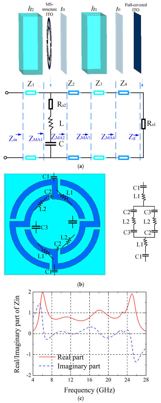
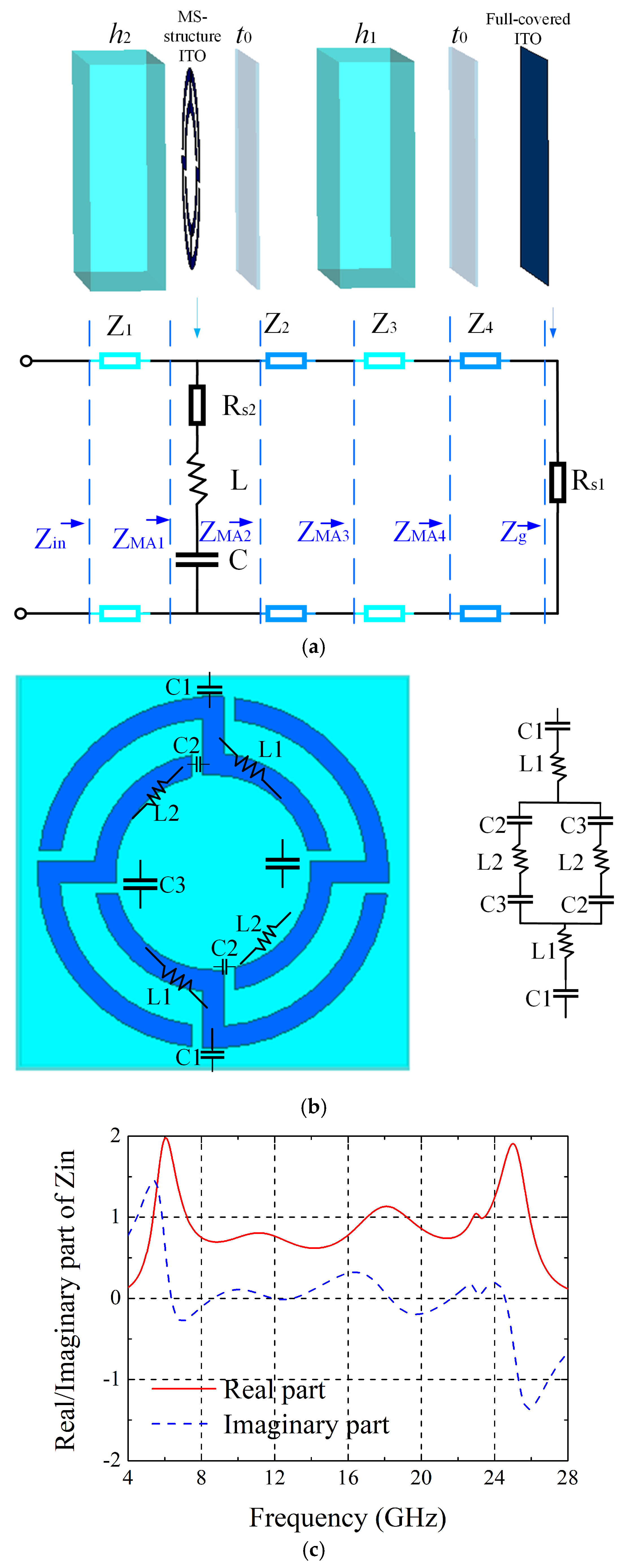
The ECM of the proposed MA is shown in Figure 5a. The top substrate made of PDMS, the middle PET, the bottom substrate made of PDMS, and the bottom PET are treated as the transmission line (length of h2, t0, h1, and t0) with certain impedance of Z1, Z2, Z3, and Z4, respectively. The MS-structure ITO is equivalent to a Rs2, L, C, and the bottom full-covered ITO ground is represented by the equivalent resistance Rs1.
Figure 5.
Analysis using ECM: (a) ECM of the proposed MA; (b) ECM of the middle MS-structure ITO film; (c) real and imaginary parts of the equivalent impedance Zin.
From the direction of the full-covered ITO ground, the impedance Zg is calculated by
Then the input impedance ZMA4 is written as
where is the propagation constant of the incident EM wave in PET, is impedance of the bottom PET substrate with the thickness of t0, and Z0 = 377 Ω is the impedance of free space.
In the same way, the impedance ZMA2 and ZMA1, and the impedance Zito of the top MS-structure ITO film can be expressed as
The impedance ZMA1 of MA can calculated as
Therefore, the total impedance Zin of MA can be calculated as
where is the propagation constant of the incident EM wave in PDMS.
It is noted that the absorption is 100% when the total input impedance Zin equals to Z0. Figure 5b gives the general ECM of the middle MS-structure ITO film. The L and C are determined by the length, width, and gap sizes of the MS topology. Therefore, the MS-structure ITO film is carefully designed to obtain a wideband and angular-stable absorption property. Figure 5b gives the real and imaginary parts of the total equivalent impedance Zin. The imaginary part values are zero at the frequencies of 6.30, 8.67, 12.43, 18.35, 21.75, and 24.6 GHz, and the corresponding real part values are 1.85, 0.70, 0.73, 1.12, 0.75, and 1.70. Hence, the imaginary part is around zero and the real part is around 1 at the four frequencies of 8.67, 12.43, 18.35, and 21.75 GHz, which are close to the four resonances of 7.23, 11.23, 18.53, and 23.21 GHz simulated using CST in Figure 2.
2.2.2. Surface Current Distributions Analysis
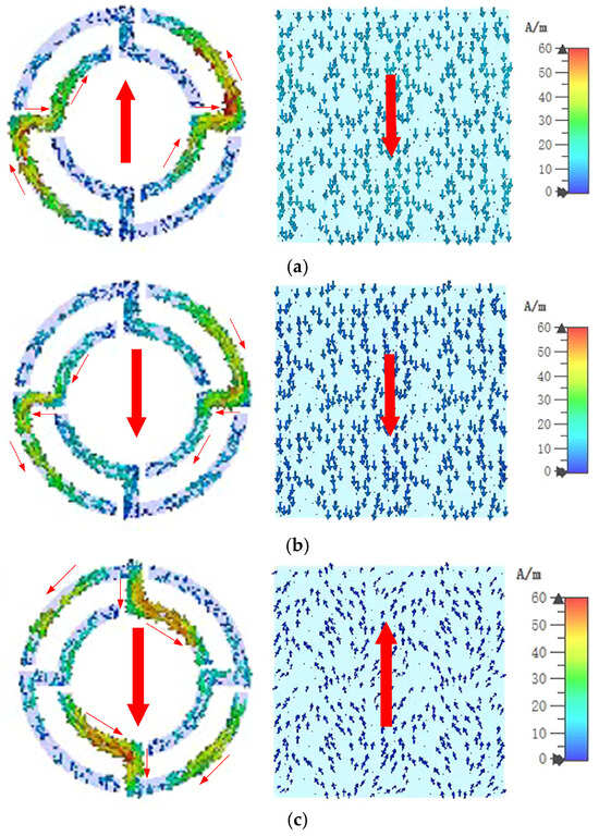
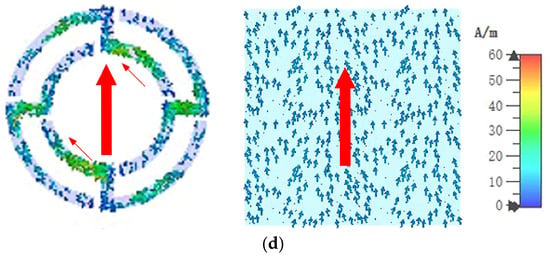
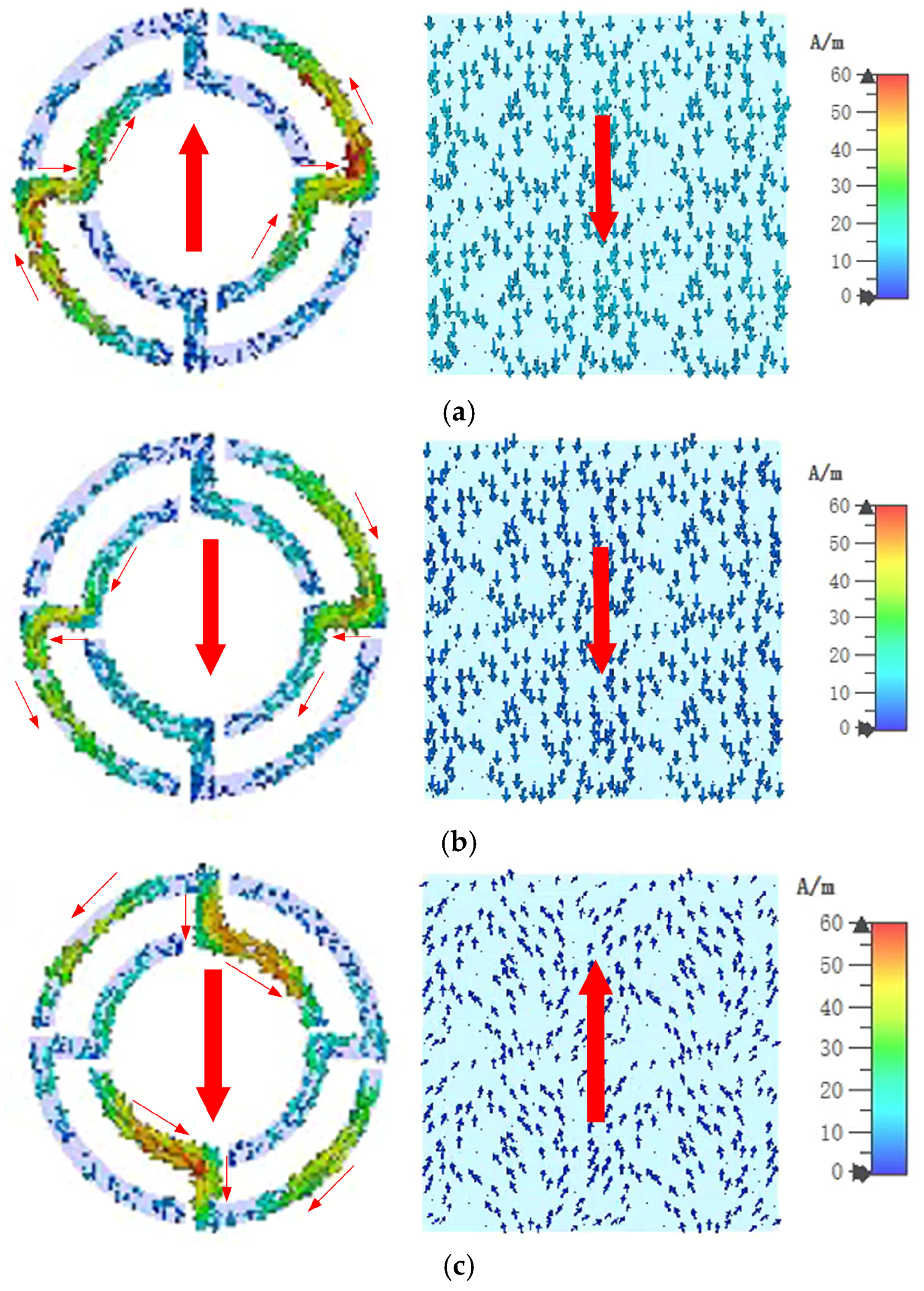
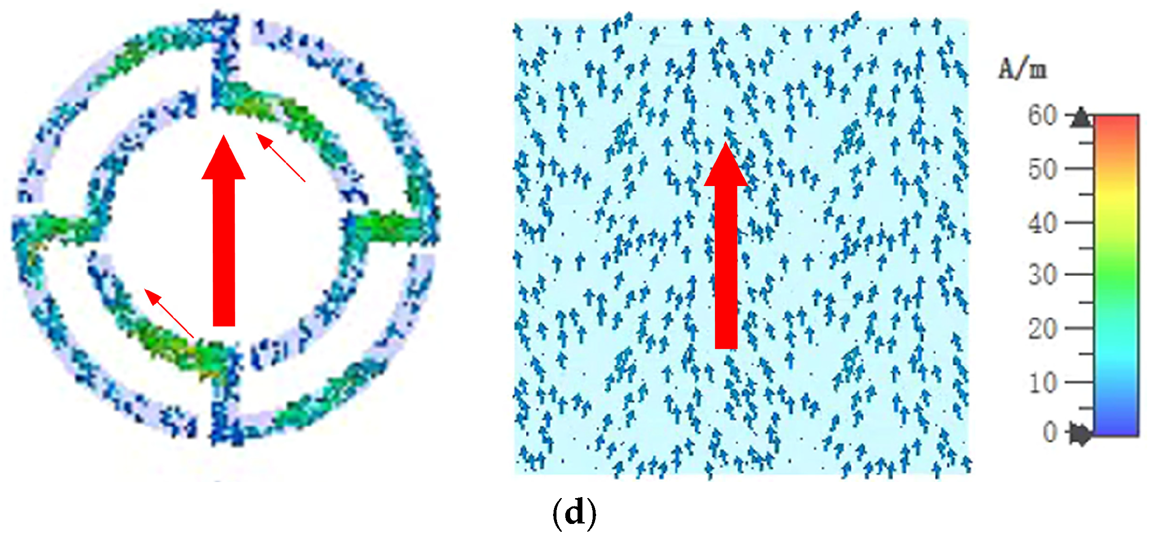
To further understand the mechanism and peak absorptivity at the four resonate frequencies, the surface current distributions at the four resonances (7.23 GHz, 11.23 GHz, 18.53 GHz, and 23.21 GHz) are displayed in Figure 6. As shown in Figure 6a, the surface currents of the middle MS-structure ITO and the bottom full-covered ITO film at 7.23 GHz are along the +y and -y directions, respectively. This indicates that a magnetic resonance is generated [19]. The strong surface currents of the MS-structure ITO are produced by the mender lines. As shown in Figure 6b, the surface currents of the middle MS-structure ITO and the bottom full-covered ITO film at 11.23 GHz are both along -y directions. This indicates that an electric resonance is generated [19]. The strong surface currents of the MS-structure ITO are produced by the mender lines. Similarly, as can be seen from Figure 6c,d, a magnetic resonance is generated at 18.53 GHz, and an electric resonance is generated at 23.21 GHz. For the third and fourth resonances, the strong surface currents of the MS-structure ITO are mainly produced by the inner parts of mender lines. The wideband is obtained by the combination of multiple electric and magnetic resonances.
Figure 6.
Surface currents of the middle and bottom ITO films: (a) 7.23 GHz, (b) 11.23 GHz, (c) 18.53 GHz, and (d) 23.21 GHz.
2.2.3. Parameter Studies
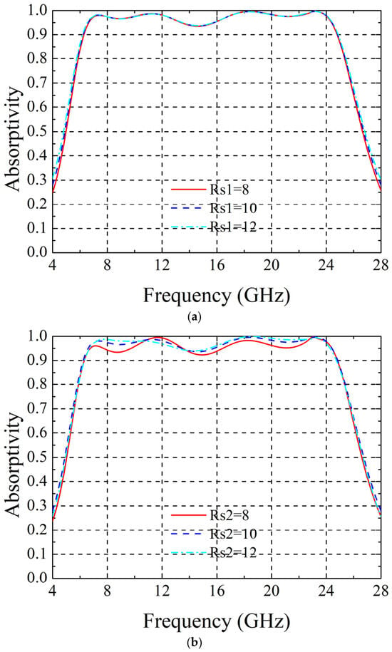
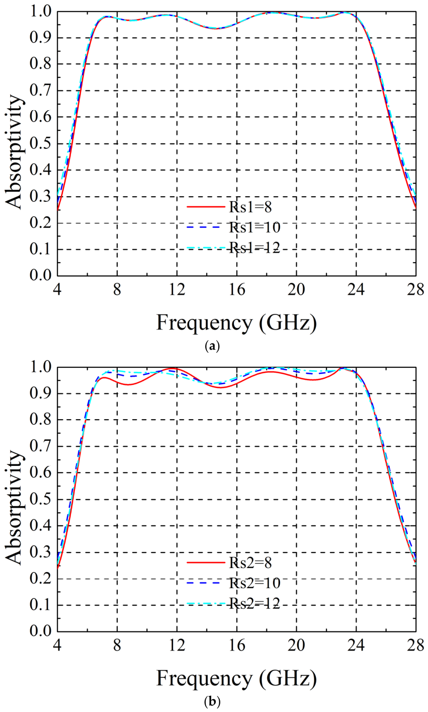
To guide the design of the MS, the parameters of the sheet resistances of the ITO films, which are always be discrepancy due to the limitations of the fabrication are analyzed. As shown in Figure 7a, when the sheet resistance of the bottom film Rs1 varies from 8 to 10 Ω/sq, the absorptivity remains unchanged. As shown in Figure 7b, when the sheet resistance of the middle MA-structure ITO film Rs2 varies from 8 to 12 Ω/sq, the first resonant frequency shifts to the higher region, and the >90% absorption bandwidth remains the same. These results indicate that the proposed MS has good robustness.
Figure 7.
Simulated absorption under different sheet resistances: (a) Rs1; (b) Rs2.
3. Results and Discussion
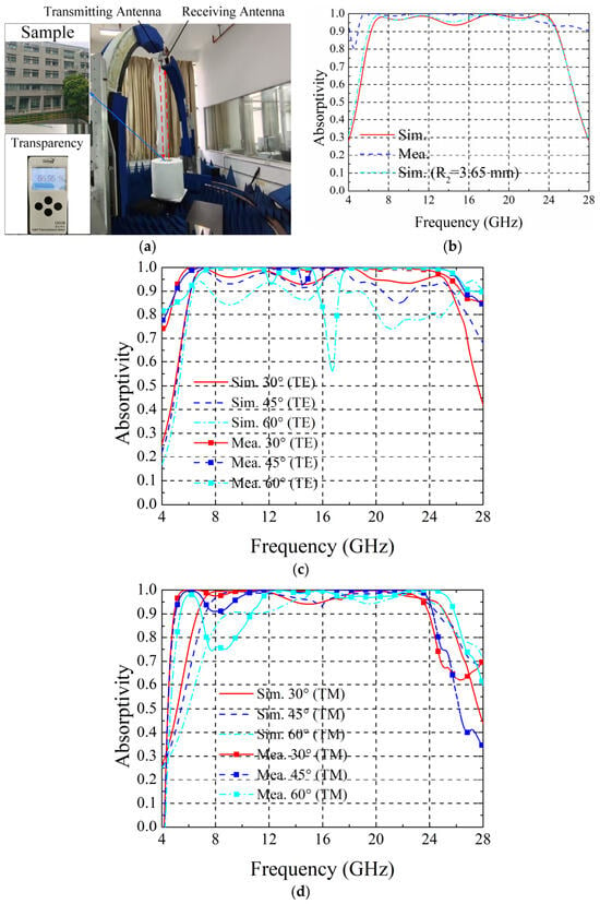
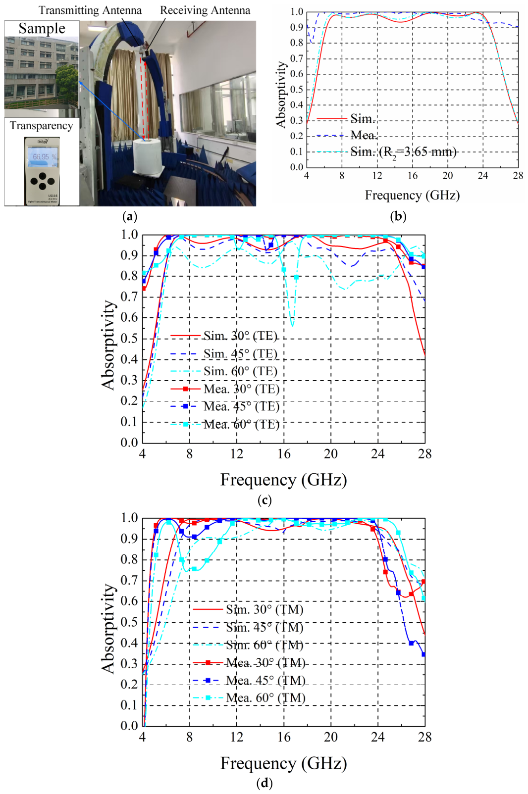
A sample consisting of 25 × 25 unit cells with a size of 225 mm × 225 mm was fabricated and measured. The light transmittance was measured by using a transmittance meter, and the reflection coefficient |S11| was measured in an anechoic chamber, as shown in Figure 8a. The transmission coefficient was not measured due to the fact that the transmission coefficient |S21| is less than 0.1 and A = 1 − |S11|2 − |S21|2 ≈ 1 − |S11|2. The wavelength range is 380~760 nm. In the measurement setup, two pairs of standard horn antennas work as the transmitting and receiving antennas, respectively. Several horn antennas were used to cover the target band from 4 GHz to 28 GHz. The distance between the sample and the horn antenna is over 2 m, which satisfies the far-field requirement. An equal-sized metallic plate was used as a reference to reduce the influence of the environmental noise.
Figure 8.
Measured results: (a) photo, light transparency, and measurement setup in an anechoic chamber; (b) measured absorptivity and error analysis under a y-polarized incident EM wave; (c) measured absorptivity under TE polarization at oblique incidences; (d) measured absorptivity under TM polarization at oblique incidences.
It can be seen from Figure 8a that the measured light transmittance is 66.95%. The ITO resistance measured by four-point probe meter is 7.8125 Ω/sq. Figure 8b shows the measured absorptivity under a y-polarized normally incident EM wave. The measured bandwidth of over 90% absorptivity is from 5 to 28 GHz, which is in reasonable agreement with the simulated one. The differences between the measurement and the simulation are attributed to the fabrication discrepancies of ITO resistance, misalignments of the horn antennas, the coupling between the transmitting and receiving antennas, and diffractions caused by the finite structure. For example, when the size R2 increases from 3.55 mm to 3.65 mm, the absorptivity values in the lower band extend, but the higher band remains unchanged. The measured absorptivity under oblique incidences of TE and TM polarizations is shown in Figure 8c and Figure 8d, respectively. It is shown that the measured absorptivity is in good agreement with the simulation within the incident angle of 45° under both TE and TM polarizations.
A performance comparison of the proposed MA and previous designs is given in Table 1. Compared with two-layered ITO designs in [27,30,35], the proposed MA has a broader absorption bandwidth. Compared with two-layered ITO designs in [39], the proposed MA has an angular stability. Compared with the two-layered ITO deposited on glasses [37,40], the proposed MA using PDMS also shows wideband and angular stability. Compared with the work in [41], the proposed MA has a lower profile and an angular stability. The proposed transparent MA has the advantages of wideband, polarization insensitivity, and angular stability, making it suitable for transparent devices of RCS reduction platforms.
Table 1.
Comparison of transparent absorber in the literature.
4. Conclusions
An optically transparent, broadband, and angular-stable MA using ITO is proposed. The broadband and wide-angle absorption performance is obtained based on the ECM, surface current distributions, and parameter studies in theory, physical insight, and practical design. Multiple magnetic and electric resonances are excited by the proposed patterned ITO. Over 90% absorptivity from 6.26 GHz to 24.86 GHz with a fractional bandwidth of 119.54% under normal incidence is achieved, and a good angular stability under oblique incidence is ensured. The measured results demonstrate that a 66.95% light transmittance, and good absorptivity performance for both normally and obliquely incident EM waves, indicating it can be a candidate for transparent RCS reduction platforms and electromagnetic shielding. The proposed mechanical analysis and design process are also beneficial to other designs working at millimeter and terahertz bands.
Author Contributions
Conceptualization, M.M. and Y.W.; methodology, M.M.; software, M.M.; validation, Y.L., X.Y., S.X., S.Y. and D.W.; formal analysis, M.M.; investigation, M.M.; resources, M.M.; data curation, M.M.; writing—original draft preparation, M.M.; writing—review and editing, J.Y., H.C. and Q.Z.; visualization, M.M.; supervision, Y.W.; project administration, M.M.; funding acquisition, Y.W. All authors have read and agreed to the published version of the manuscript.
Funding
This research received no external funding.
Institutional Review Board Statement
Not applicable.
Informed Consent Statement
Not applicable.
Data Availability Statement
The raw data supporting the conclusions of this article will be made available by the authors on request.
Conflicts of Interest
The authors declare no conflicts of interest.
References
- Knott, E.F.; Shaeffer, J.F.; Tuley, M.T. Radar Cross Section; SciTech: Raleigh, NC, USA, 2004. [Google Scholar]
- Li, J.; Zhou, D.; Wang, P.-J.; Du, C.; Liu, W.-F.; Su, J.-Z.; Pang, L.-X.; Cao, M.-S.; Kong, L.-B. Recent progress in two-dimensional materials for microwave absorption applications. Chem. Eng. J. 2021, 425, 131558. [Google Scholar] [CrossRef] [Scilit]
- Sleasman, T.; Duggan, R.; Awadallah, R.S.; Shrekenhamer, D. Dual-resonance dynamic metasurface for independent magnitude and phase modulation. Phys. Rev. Appl. 2023, 20, 014004. [Google Scholar] [CrossRef] [Scilit]
- Wang, Z.X.; Xu, H.; Lv, J.M.; Liu, S.; Dai, J.Y.; Wu, J.W.; Cheng, Q.; Cui, T.J. High-resolution phase-magnitude-decoupled information metasurface for complex beamforming and dual channel 16 QAM secure communication. Adv. Funct. Mater. 2025, 35, 2503273. [Google Scholar] [CrossRef] [Scilit]
- Zheng, Q.; Jiang, H.; Wang, Y.; Yang, X.-X.; Pang, X. Metasurface-FSS-integrated stealth radome based on photonic spin hall effect. IEEE Antennas Wirel. Propag. Lett. 2026, 25, 2748–2752. [Google Scholar] [CrossRef] [Scilit]
- Fu, S.; Yang, X. A terahertz four-band high-sensitivity perfect absorber based on Dirac semimetal. Phys. Lett. A 2026, 587, 131760. [Google Scholar] [CrossRef] [Scilit]
- Lin, Z.; Sun, L.; Cheng, S.; Tang, C.; Gao, F.; Li, B. Five-band tunable terahertz AlCuFe metasurface absorber with high refractive index sensitivity based on surface plasmon resonance. Physica B Condens. Matter 2026, 744, 419512. [Google Scholar] [CrossRef] [Scilit]
- Fu, Z.; Chen, Y.; Shi, F.; Jin, R.; Guo, J.; Zhang, Y.; Yu, F.; Chen, J.; Huang, L.; Zhou, C.; et al. High-order photonic degeneracy enables topological reconfiguration in bound states in the continuum. Nat. Commun. 2026, 17, 9203. [Google Scholar] [CrossRef] [Scilit] [PubMed]
- Ni, S.; Li, X.; Chen, R.; Zhu, F.; Pan, C.; Mi, S.; Fan, X.; Guan, H.; Tang, W.; Wang, L.; et al. Symmetry-cooperative optical-field engineering for ultrabroadband bulk photovoltaic photodetection. Nat. Commun. 2026, 17, 10595. [Google Scholar] [CrossRef] [Scilit] [PubMed]
- Gu, X.; Zhang, Y.; You, S.; Fu, Z.; Ni, B.; Chang, J.; Ni, H.; Chen, X.; Lu, W.; Li, G.; et al. Dual-point-groups engineering enable multi-ultrahigh-Q resonances via Brillouin zone folding in tetramer metasurfaces. Nat. Commun. 2026. Early access. [Google Scholar] [CrossRef] [Scilit]
- Wang, J.; Wang, J.; Yu, F.; Chen, J.; Chen, R.; Geng, T.; Jin, R.; Zhou, Y.; Zheng, T.; Li, G.; et al. Continuous polarization–wavelength mapping with nonlocal metasurfaces. Light Sci. Appl. 2026, 15, 170. [Google Scholar] [CrossRef] [Scilit] [PubMed]
- Luo, Z.; Shan, X.; Ren, X.; Wu, K.; Chen, Y.; Hong, L.; Ma, H.F.; Cheng, Q.; Cui, T.J. Active Metasurface Absorber for intensity-dependent surface-wave shielding. IEEE Trans. Antennas Propag. 2023, 71, 5795–5804. [Google Scholar] [CrossRef] [Scilit]
- Narayanaswamy, N.K.; Satheesha, T.Y.; Alzahrani, Y.; Pandey, A.; Dwivedi, A.K.; Singh, V.; Tolani, M. Metasurface absorber for millimeter waves: A deep learning-optimized approach for enhancing the isolation of wideband dual-port MIMO antennas. Sci. Rep. 2024, 14, 30199. [Google Scholar] [CrossRef] [Scilit] [PubMed]
- Zhou, Q.; Ma, W.; Wu, T.; Li, Y.; Qiu, Q.; Duan, J.; Li, J.; Jiang, L.; Zhou, W.; Gao, Y.; et al. Metasurface terahertz perfect absorber with strong multi-frequency selectivity. ACS Omega 2022, 7, 36712–36727. [Google Scholar] [CrossRef] [Scilit] [PubMed]
- Landy, N.I.; Sajuyigbe, S.; Mock, J.J.; Smith, D.R.; Padilla, W.J. Perfect metamaterial absorber. Phys. Rev. Lett. 2008, 100, 207402. [Google Scholar] [CrossRef] [Scilit] [PubMed]
- Shang, Y.; Shen, Z.; Xiao, S. On the design of single-layer circuit analog absorber using double-square-loop array. IEEE Trans. Antennas Propag. 2013, 61, 6022–6029. [Google Scholar] [CrossRef] [Scilit]
- Nochian, P.; Atlasbaf, Z. A novel single layer ultra-wideband metamaterial absorber. Prog. Electromagn. Res. 2020, 93, 107–114. [Google Scholar] [CrossRef] [Scilit]
- Khanna, Y.; Awasthi, Y.K. A single layer wideband metasurface absorber for electromagnetic interference minimization in Ku-band applications. Int. J. Microw. Wirel. Technol. 2022, 14, 573–579. [Google Scholar] [CrossRef] [Scilit]
- Beeharry, T.; Yahiaoui, R.; Selemani, K.; Ouslimani, H.H. A dual layer broadband radar absorber to minimize electromagnetic interference in radomes. Sci. Rep. 2018, 8, 382. [Google Scholar] [CrossRef] [Scilit] [PubMed]
- Lim, D.; Lim, S. Ultrawideband electromagnetic absorber using sandwiched broadband metasurfaces. IEEE Antennas Wirel. Propag. Lett. 2019, 18, 1887–1891. [Google Scholar] [CrossRef] [Scilit]
- Zhang, D.; Chen, Y.; Zhou, Q. Multilayer broadband metamaterial for microwave absorption based on resistive frequency selective surfaces. Results Phys. 2025, 73, 108261. [Google Scholar] [CrossRef] [Scilit]
- Lei, Y.; Jia, X.; Zhang, J.; Hu, J.; Kang, Y.; Zou, T. An ultra-broadband multi-layer dielectric gradient honeycomb microwave absorber enhanced by the double layer metasurface. Opt. Mater. 2024, 156, 116009. [Google Scholar] [CrossRef] [Scilit]
- Soghi, S.; Heidar, H.; Haraty, M.R.; Nayyeri, V. Single-layer broadband optically transparent metamaterial absorber using gold thin film. IEEE Trans. Microw. Theory Tech. 2024, 72, 3743–3752. [Google Scholar] [CrossRef] [Scilit]
- Xu, H.; Cheng, J.; Huang, Q.; Luo, M.; Li, D.; Zhu, D.; Zhan, G.; Zheng, Q.; Zhang, Y.; Shao, J.; et al. Flexible broadband metamaterial absorber in long-wave infrared with visible transparency fabricated by laser direct writing. Opt. Lett. 2024, 49, 89–92. [Google Scholar] [CrossRef] [Scilit] [PubMed]
- Kim, J.; Jepiti, P.; Lee, M.; Park, E.; Phon, R.; Lim, S. Screen-printing high/low resistance using only a single silver nanowire ink: Resistance-gradient metasurface application for broadband microwave absorption and optical transparency. Mater. Des. 2024, 247, 113451. [Google Scholar] [CrossRef] [Scilit]
- Zhou, Q.; Xue, B.; Gu, S.; Ye, F.; Fan, X.; Duan, W. Ultra broadband electromagnetic wave absorbing and scattering properties of flexible sandwich cylindrical water-based metamaterials. Results Phys. 2022, 38, 105587. [Google Scholar] [CrossRef] [Scilit]
- Deng, R.; Zhang, K.; Li, M.; Song, L.; Zhang, T. Targeted design, analysis and experimental characterization of flexible microwave absorber for window application. Mater. Des. 2019, 162, 119–129. [Google Scholar] [CrossRef] [Scilit]
- Min, P.; Song, Z.; Yang, L.; Dai, B.; Zhu, J. Transparent ultra-wideband absorber based on simple patterned resistive metasurface with three resonant modes. Opt. Express 2020, 28, 19518–19530. [Google Scholar] [CrossRef] [Scilit] [PubMed]
- Jiang, H.; Yang, W.; Lei, S.; Hu, H.; Chen, B.; Bao, Y.; He, Z. Transparent and ultra-wideband metamaterial absorber using coupled hexagonal combined elements. Opt. Express 2021, 29, 29439–29448. [Google Scholar] [CrossRef] [Scilit] [PubMed]
- Li, S.; Liu, L.; Jiang, Y.; Tang, C.; Gu, C.; Li, Z. Ultrathin optically transparent electromagnetic shielding window with broadband microwave absorption and ultrahigh optical transmittance. Int. J. RF Microw. Comput. Aided Eng. 2022, 32, e23338. [Google Scholar] [CrossRef] [Scilit]
- Lai, S.; Guo, Y.; Liu, G.; Liu, Y.; Fu, C.; Chang, H.; Wu, Y.; Gu, W. A high-performance ultra-broadband transparent absorber with a patterned ITO metasurface. IEEE Photon. J. 2022, 14, 4629107. [Google Scholar] [CrossRef] [Scilit]
- Song, N.; Sun, Q.; Xu, S.; Shan, D.; Tang, Y.; Tian, X.; Xu, N.; Gao, J. Ultrawide-band optically transparent antidiffraction metamaterial absorber with a Thiessen-polygon metal-mesh shielding layer. Photonics Res. 2023, 11, 1354. [Google Scholar] [CrossRef] [Scilit]
- Ge, J.; Zhang, Y.; Li, H.; Dong, H.; Zhang, L. Ultra-broadband tunable and transparent microwave meta-absorber using ITO and water substrate. Adv. Opt. Mater. 2023, 11, 2202873. [Google Scholar] [CrossRef] [Scilit]
- Zheng, J.; Zheng, H.; Pang, Y.; Qu, B.; Xu, Z. Transparent broadband absorber based on a multilayer ITO conductive film. Opt. Express 2023, 31, 3731–3742. [Google Scholar] [CrossRef] [Scilit] [PubMed]
- Zheng, Q.; Qi, J.; Ma, J.; PourMohammadi, P.; Li, Q. Optically transparent wideband metamaterial absorber based on equivalent aperture and characteristic mode analysis. J. Appl. Phys. 2024, 135, 043101. [Google Scholar] [CrossRef] [Scilit]
- Dong, X.Y.; Su, W.Q.; Ruan, Y.; Cui, H.Y.; Chen, L. Ultra-wideband metasurface absorber based on ITO material. J. Appl. Phys. 2025, 138, 143101. [Google Scholar] [CrossRef] [Scilit]
- Mo, M.; Wang, Y.; Xie, S.; Huang, D.; Liu, Y.; Wang, D.; Yang, J.; Zheng, Q. Ultra-broadband and optically transparent metamaterial-based absorber for electromagnetic absorption/shielding. J. Appl. Phys. 2025, 137, 133102. [Google Scholar] [CrossRef] [Scilit]
- Zhang, J.; Zhang, S.; Dong, J.; Wang, M.; Luo, H.; Wu, R.; Xiao, C. Design of an ultra-wideband flexible optically transparent metamaterial absorber with wide-angle and polarization stability. Mater. Des. 2025, 253, 113921. [Google Scholar] [CrossRef] [Scilit]
- Zhao, C.; Jia, M.; Zhang, N.; Meng, S.; Tian, Y. Ultra-wideband optically transparent flexible metamaterial absorber for satellite RCS Reduction. Sci. Rep. 2025, 15, 29093. [Google Scholar] [CrossRef] [Scilit] [PubMed]
- Mo, M.; Wang, Y.; Xie, S.; Huang, D.; Liu, Y.; Wang, D.; Yang, J.; Zheng, Q. Wideband and wide-angle optically transparent metamaterial-based absorber for radar cross section reduction. J. Electron. Mater. 2025, 54, 3147–3160. [Google Scholar] [CrossRef] [Scilit]
- Zheng, L.; Li, M.; Li, W.; Wang, T.; Wang, X.; Gong, R. Optical transparent ultrabroadband metamaterial absorber with matching layer and gradient impedance. IEEE Antennas Wirel. Propag. Lett. 2025, 24, 2262–2266. [Google Scholar] [CrossRef] [Scilit]
- Alwan, E.A.; Kiourti, A.; Volakis, J.L. Indium tin oxide film characterization at 0.1–20 GHz using coaxial probe method. IEEE Access 2015, 3, 648–652. [Google Scholar] [CrossRef] [Scilit]
- Hussain, M.; Zahra, H.; Abbas, S.M.; Zhu, Y. Flexible dielectric materials: Potential and applications in antennas and RF sensors. Adv. Electron. Mater. 2024, 10, 2400240. [Google Scholar] [CrossRef] [Scilit]

Disclaimer/Publisher’s Note: The statements, opinions and data contained in all publications are solely those of the individual author(s) and contributor(s) and not of MDPI and/or the editor(s). MDPI and/or the editor(s) disclaim responsibility for any injury to people or property resulting from any ideas, methods, instructions or products referred to in the content. |
© 2026 by the authors. Licensee MDPI, Basel, Switzerland. This article is an open access article distributed under the terms and conditions of the Creative Commons Attribution (CC BY) license.