


Abstract
4-inch Cu/Cu wafer bonding with sequential plasma activation was investigated at 200 °C, and the effects of bonding atmosphere and Cu grain size on the bonding were investigated. With sequential plasma activation, the bonding atmosphere primarily affected the thickness of the interfacial oxide layer and may also have influenced its composition at the normal-grain Cu/Cu bonded interface. When bonding was performed in air, the interfacial oxide layer was approximately 80 nm thick and consisted mainly of Cu2O, with XPS suggesting a small amount of CuO on the debonded surfaces. In contrast, for bonding conducted under a vacuum of 1000 Pa, an approximately 10 nm thick Cu2O layer was observed. Although their bond strengths were comparable, wafer fracture during bond strength measurements of the vacuum-bonded Cu/Cu wafers suggested stronger interfacial bonding. With Ar ion beam treatment combined with sequential plasma activation, Cu grain size greatly affected the bonded interface. For fine-grain Cu wafers with grain size smaller than 100 nm, an oxide-free and nitride-free bonded interface was obtained, and Cu grain growth across the interface occurred, leading to strong interfacial bonding. However, for normal-grain Cu wafers with grain size of 200 nm–600 nm, an approximately 15 nm thick Cu2O layer was found at the bonded interface, and the bond strength was as low as 0.6 J/m2.
1. Introduction
Hybrid bonding, which provides a solution for fine pitches of sub-10 µm with the shortest vertical interconnection, can achieve a high-level power and signal integration [1,2,3]. During the process, dielectric SiO2/SiO2 bonding is first achieved by hydrophilic bonding. Then, post-annealing is conducted to obtain sufficient bond strength. Meanwhile, Cu pads on the upper and lower wafers come into contact and are bonded by diffusion bonding. The commonly used post-annealing temperature is 350–400 °C. However, this temperature is too high for some devices [4,5]. Therefore, low-temperature hybrid bonding processes have attracted significant interest.
To achieve low-temperature SiO2/Cu hybrid bonding, the key challenge is the simultaneous realization of low-resistance Cu/Cu bonding and strong SiO2/SiO2 bonding. For Cu/Cu bonding, due to the much higher resistivity of copper oxide and copper nitride, the essence of low resistance is to create an oxide-free and nitride-free bonded interface. To remove the native oxide on the Cu surface, various pre-treatments, such as acid treatment [6,7,8], formic acid vapor treatment [9,10], and Ar ion beam irradiation [11,12], have been reported. However, these methods are not effective in improving the bond strength of SiO2/SiO2 [13]. Passivation of the Cu surface with self-assembled monolayers (SAMs) [14,15,16], metal layers [17,18] or CuxN [19,20] has also been reported. Nevertheless, SAMs were difficult to desorb completely below 250 °C, and the fabrication process of metal passivation layer was complex. Passivated by Cu4N through two-step Ar/N2 plasma, Cu/Cu bonding succeeded at 260 °C [21], but many fine voids appeared in SiO2/SiO2 bonding [22]. Moreover, when the bonding temperature decreased to 220 °C, large unbonded areas were observed in Cu/Cu bonding due to the insufficient decomposition of copper nitride [23].
Another approach to designing the low-temperature Cu/SiO2 bonding process is to start from the SiO2 side. Since NaOH could improve the bond strength of SiO2/SiO2 bonding through an increase in Si-OH groups on the SiO2 surface, nanotwin Cu/SiO2 hybrid wafers treated sequentially with NaOH, HCl, and NaOH were successfully bonded at 200 °C [24,25,26]. Without HCl treatment, Cu/SiO2 hybrid wafers should be bonded within 24 h after CMP to avoid Cu oxidation and contamination. Cu/Cu interface was completely sealed at 150 °C, but a 5 nm thick oxide layer was occasionally observed at the interface when the post-annealing temperature decreased to 100 °C [24]. We demonstrated that the bond strength of SiO2/SiO2 could also be increased by sequential plasma activation of O2 plasma, N2 plasma and N radical [27]. Unfortunately, an ~80 nm thick oxide layer formed at the Cu/Cu interface after being post-annealed at 200 °C. When the bonding atmosphere was changed from air to a vacuum of 1000 Pa, oxide layer thickness decreased greatly, but 15 nm still existed [28].
Based on our previous research regarding Cu/Cu wafer bonding at 200 °C with sequential plasma, we further investigated the influence of bonding atmosphere on the bond strength and interfacial structure. To completely understand the applicability of sequential plasma for low-temperature Cu/Cu bonding, an Ar ion beam was used to remove the native oxide on the Cu surface, and the effects of Cu microstructure on Cu/Cu bonding were compared.
2. Materials and Methods
4-inch Cu wafers were prepared according to the following steps. Firstly, a 25 nm thick Ti film was deposited on 525 µm-thick (100) Si wafers as an adhesion and barrier layer, followed by a 1 µm-thick sputtered Cu layer. Then, the Cu surface was smoothed by CMP, which reduced the Cu film thickness to approximately 820–880 nm. The Si wafers were supplied by D-process Inc. (Tokyo, Japan), which also performed Ti/Cu film deposition and CMP. These Cu wafers were named normal-grain Cu wafers. To prepare fine-grain Cu wafers, the thicknesses of Ti and Cu layers were reduced to 10 nm and 25 nm, respectively. The Si wafers were supplied by Kyushu Semiconductor KAW Co., Ltd. (Kitsuki, Japan), and the deposition of metal layers was performed by Kyodo International, Inc. (Kawasaki, Japan). After deposition, CMP was not performed. The Cu grain size and surface roughness of the two types of Cu wafers were investigated by scanning electron microscopy (SEM, SU8600, Hitachi, Tokyo, Japan) and dynamic force microscopy (DFM, L-traceII, Hitachi, Tokyo, Japan), respectively.
To compare the effect of bonding atmosphere on Cu/Cu wafer bonding, normal-grain Cu wafers were activated by sequential plasma (WP100, BondTech Co., Ltd., Kyoto, Japan), including O2 plasma, N2 plasma and N radicals. The plasma power and irradiation time for all plasma treatments were fixed at 250 W and 15 s, respectively. After the plasma activation, the Cu wafers were placed on a Peltier cooling stage (CT-100, BondTech Co., Ltd., Kyoto, Japan) in ambient air to enhance surface hydrophilicity. The stage temperature was set to 12.2 °C, corresponding to an estimated local relative humidity of approximately 90% near the wafer surface under the experimental ambient conditions. The wafers were held on the stage for 30 s and then bonded in air or under a vacuum of 1000 Pa at a pressure of 2.5 MPa for 60 s by a bonder (WF3000, BondTech Co., Ltd., Kyoto, Japan). Finally, post-annealing was carried out in an oven (SH-DO-150FH, SH Scientific, Sejong, Republic of Korea) in an N2 atmosphere at 200 °C for 7 h.
Ar ion beam with an etching rate of 2 nm/min installed in a bonder (No. 11, BondTech Co., Ltd., Kyoto, Japan) was used to sputter away the native oxide on the Cu wafer surface. Normal-grain and fine-grain Cu wafers were irradiated by an Ar ion beam for 5 min, followed by sequential plasma activation. After Peltier cooling, the two types of Cu wafers were pre-bonded in air for 60 s, followed by a thermo-compression process under vacuum at 1.3 MPa and 200 °C for 2 h. Post-annealing was conducted under the same conditions as described above.
After bonding, the bond strength of Cu/Cu wafers was evaluated using the crack-opening method [29]. A blade with a thickness of 100 µm was manually inserted into the bonded interface to a depth of approximately 5 mm along an in-plane <110> direction of Si wafers. The crack length was determined from the surface acoustic tomography (SAT, FS300 III, Hitachi, Tokyo, Japan) image acquired 180 s after blade insertion was stopped. The bond strength, expressed as the surface energy, was calculated using Equation (1) [30]:
where γ, d, a, h, E, and ν denote the surface energy, blade thickness (1 × 10⁻⁴ m), crack length, wafer thickness (5.25 × 10⁻⁴ m), Young’s modulus (1.69 × 10¹¹ Pa), and Poisson’s ratio (0.064), respectively. The values of E and ν correspond to the in-plane ⟨110⟩ direction of (100) Si wafers. After debonding, the exposed Cu surfaces were analyzed by X-ray photoelectron spectroscopy (XPS, JPS-9200T, JEOL Ltd., Tokyo, Japan). The cross-sectional microstructures were characterized by scanning transmission electron microscopy (STEM, JEM-ARM200F, JEOL Ltd., Tokyo, Japan) combined with energy-dispersive X-ray spectroscopy (EDS) and electron energy-loss spectroscopy (EELS), and fast Fourier transform (FFT) images were generated using Gatan DigitalMicrograph 3.9.0.
3. Results and Discussion
3.1. Effect of Bonding Atmosphere on the Normal-Grain Cu/Cu Wafer Bonding
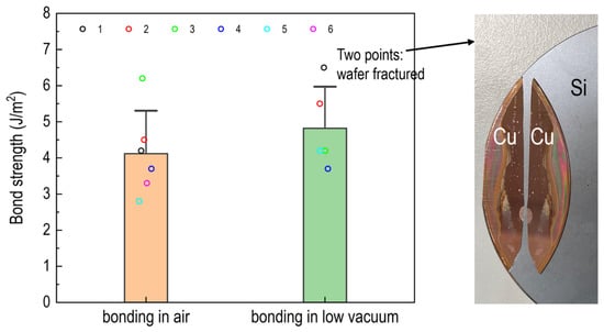
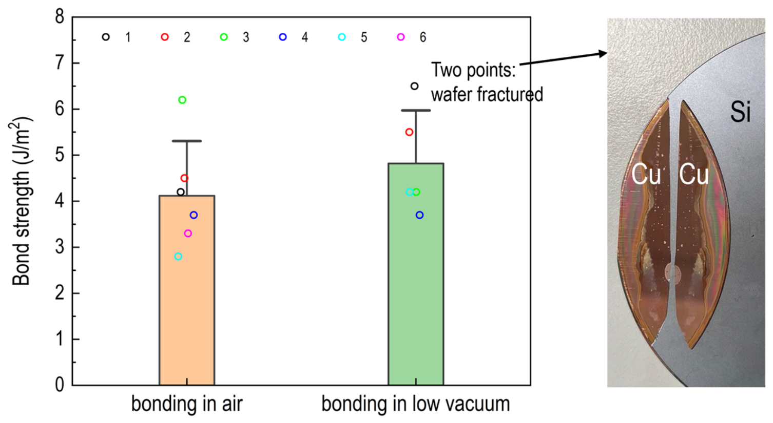
Figure 1 shows the bond strength of normal-grain Cu/Cu wafers bonded in air and under vacuum. Colorful circles represent individual measurements, while columns represent the average values with error bars. Without calculating the wafer-fractured points, the average bond strength of normal-grain Cu/Cu wafers bonded under vacuum (4.8 J/m2) was slightly higher than that bonded in air (4.1 J/m2). Considering the measurement errors, the difference was not significant. However, wafer fracture occurred at two measurement points for the vacuum-bonded Cu/Cu wafers, whereas no wafer fracture was observed for the air-bonded samples. This suggests that vacuum bonding tended to produce stronger interfacial bonding.
Figure 1.
Bond strength of normal-grain Cu/Cu wafers bonded in air and under vacuum.
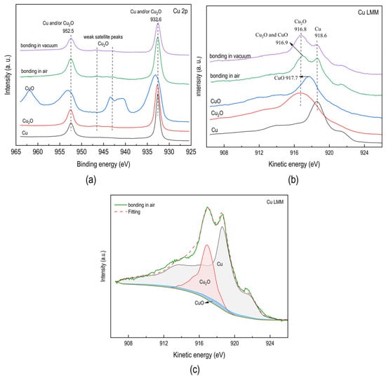
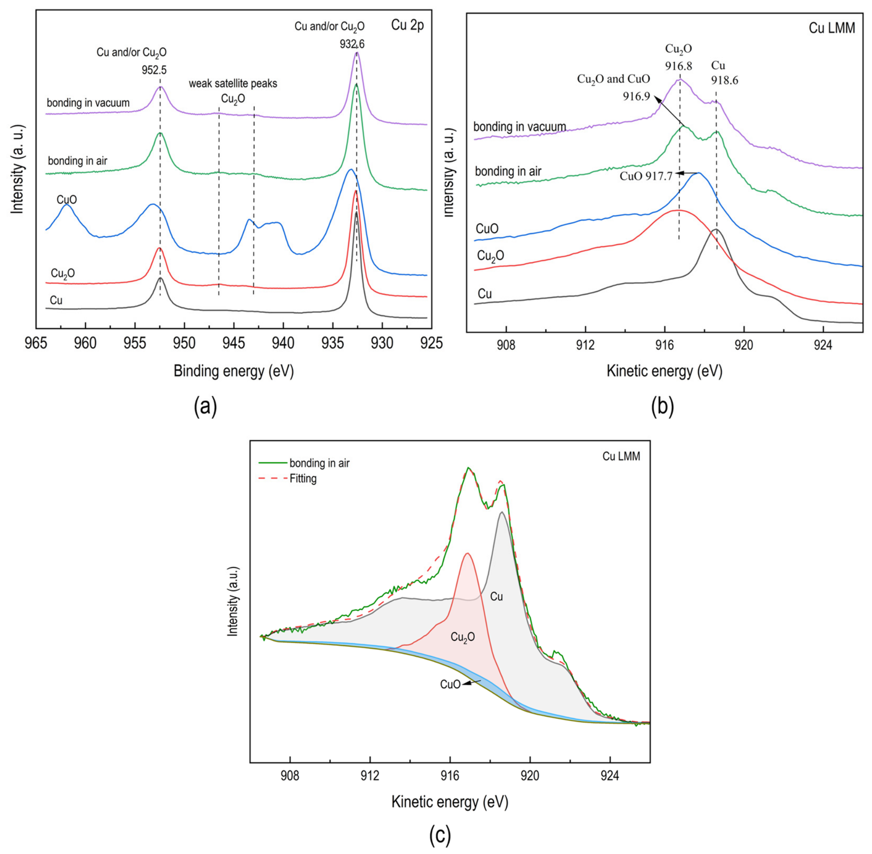
After the bonded Cu/Cu wafers were debonded using blade insertion, the exposed Cu surfaces were analyzed by XPS. The Cu 2p and Cu LMM peaks are presented in Figure 2. As shown in Figure 2a,b, the positions of the Cu 2p peaks were nearly identical for the air- and vacuum-bonded samples, while those of the Cu LMM peaks differed slightly. Cu 2p peaks at 932.6 eV and 952.5 eV, together with weak satellite peaks, indicate that Cu and/or Cu2O dominated the debonded surfaces [31]. The Cu LMM peaks at 918.6 and 916.8 eV measured from the debonded surface of the vacuum-bonded Cu/Cu wafer confirm the coexistence of metallic Cu and Cu2O and the absence of CuO [31]. In contrast, the Cu LMM peaks at 918.6 and 916.9 eV measured from the debonded surface of the air-bonded Cu/Cu wafer, together with the peak-fitting results shown in Figure 2c, suggest the presence of a minor amount of CuO in addition to metallic Cu and Cu2O.
Figure 2.
XPS analysis of debonded normal-grain Cu surfaces bonded in air and under vacuum. (a) Cu 2p binding energy spectra. (b) Cu LMM kinetic energy spectra. (c) Peak-fitting analysis of the Cu LMM spectrum measured from the air-bonded sample.
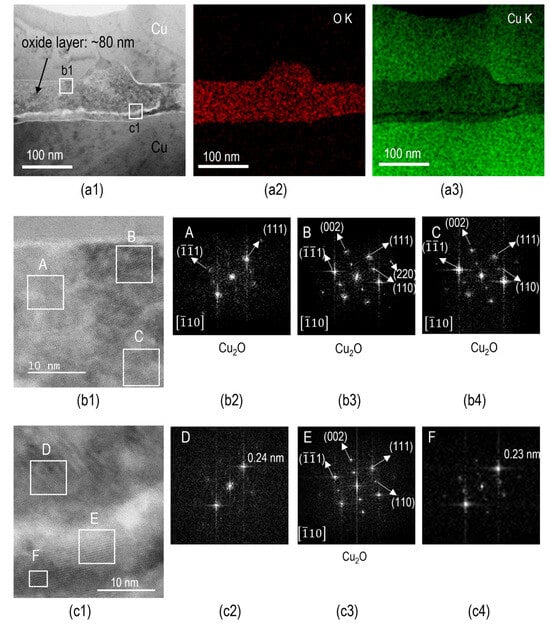
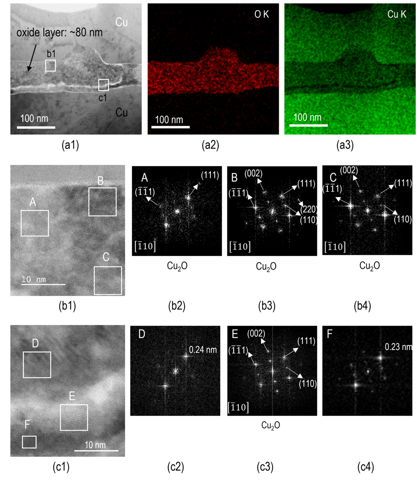
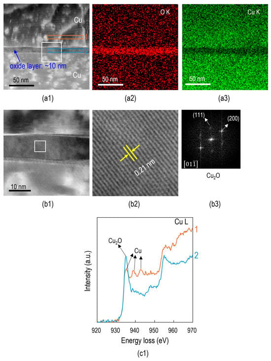
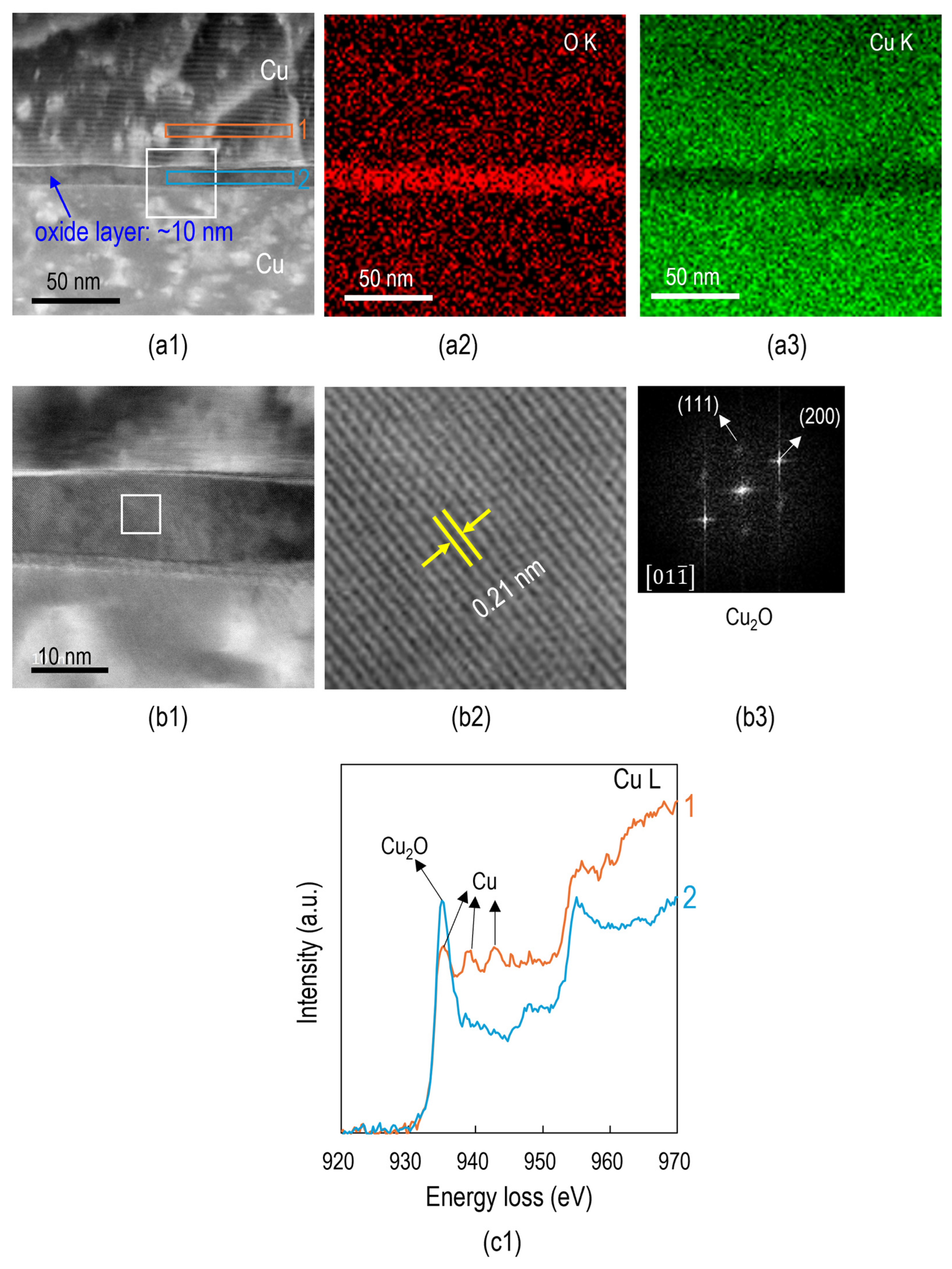
Figure 3 and Figure 4 show the cross-sectional STEM images, EDS mappings and FFT images of normal-grain Cu/Cu wafers bonded in air and under vacuum, respectively. Measured and theoretical d-spacings and inter-spot angles for the indexed FFT patterns are listed in Tables S1 and S2 in the Supplementary Materials. Figure 3(a1) and Figure 4(a1) reveal that oxide layers were present at both bonded interfaces regardless of the bonding atmosphere. However, their thicknesses differed markedly. The interfacial oxide thicknesses for the Cu/Cu wafers bonded in air and under vacuum were approximately 80 nm and 10 nm, respectively. The FFT and EELS results in Figure 4 indicate that the interfacial oxide formed under vacuum consisted primarily of Cu2O, which is consistent with the XPS results. For the sample bonded in air, several FFT patterns were assigned to Cu2O, whereas the phase assignments for the remaining patterns were inconclusive. Although XPS suggested the presence of Cu2O and a small amount of CuO, the presence of CuO could not be conclusively confirmed from the FFT patterns. Given the limited areas examined by TEM and the inconclusive phase assignments for some patterns, the presence of CuO cannot be ruled out.
Figure 3.
Cross-sectional STEM images, EDS mappings and FFT images of normal-grain Cu/Cu interface bonded in air. (a1) Cross-sectional STEM image. (a2,a3) O and Cu mappings of (a1). (b1,c1) enlarged views of (a1). (b2–b4) FFT images obtained from different areas in (b1). (c2–c4) FFT images obtained from different areas in (c1).
Figure 4.
Cross-sectional STEM images, EDS mappings and FFT images of normal-grain Cu/Cu interface bonded under vacuum. (a1) Cross-sectional STEM image. (a2,a3) O and Cu mappings of (a1). (b1) Enlarged view of the square area in (a1). (b2,b3) Enlarged view and FFT image obtained from the square area in (b1), respectively. (c1) EELS of Cu L edges for different points in (a2).
The formation and evolution of the interfacial oxides under different bonding atmospheres can be explained as follows. Because the bonding experiments were not conducted immediately after CMP, a native oxide layer is expected to have formed on the Cu surface.
After sequential plasma activation and hydrophilization treatment, the amounts of oxides and hydroxyl (-OH) groups increased. When the bonding was conducted in air, initial bonding was formed by Cu-OH groups with water included at the interface [24]. Due to the concave shape of Cu wafers, air was trapped between the two wafers. During post-annealing, Cu-OH sites were converted into Cu-O-Cu, forming oxide at the interface. At the same time, O2 in trapped air between the two wafers diffused into Cu, resulting in the oxidation reactions described by Equations (2) and (3). As O2 was consumed, the oxidation reactions gradually ceased, and the reduction of CuO into Cu2O proceeded according to Equation (4). However, CuO may have remained at the bonded interface due to incomplete reduction. In contrast, when the bonding was performed under vacuum, the amount of O2 trapped between the two Cu wafers was greatly reduced. During post-annealing, the oxidation reactions were suppressed, while the reduction of CuO was promoted [32]. Thus, no evidence of CuO was observed at the bonded interface. Because the interfacial Cu2O was not completely removed during post-annealing, Cu2O remained at both bonded interfaces.
2 Cu + 1/2 O2 → Cu2O
Cu2O + 1/2 O2 → 2 CuO
CuO + Cu → Cu2O
3.2. Effect of Cu Grain Size on Cu/Cu Wafer Bonding in Air
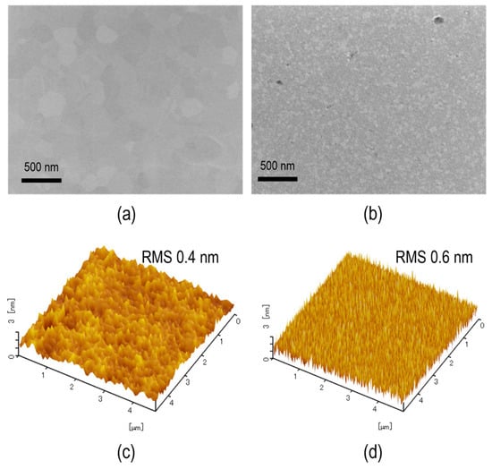
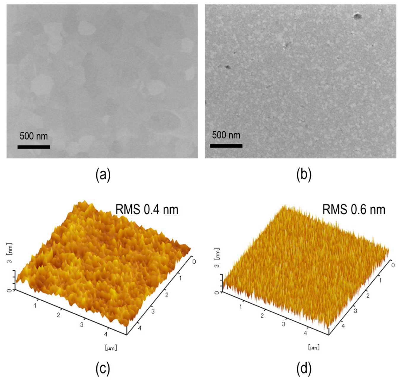
SEM and SPM images of normal-grain and fine-grain Cu surfaces are shown in Figure 5. The Cu grain sizes were 200–600 nm and several tens of nanometers, respectively. The corresponding root-mean-square (RMS) roughness values measured over a 5 × 5 µm2 area were 0.4 nm and 0.6 nm.
Figure 5.
SEM and SPM images of normal-grain and fine-grain Cu wafers. (a,b) SEM images of normal-grain and fine-grain Cu. (c,d) SPM images of normal-grain and fine-grain Cu.
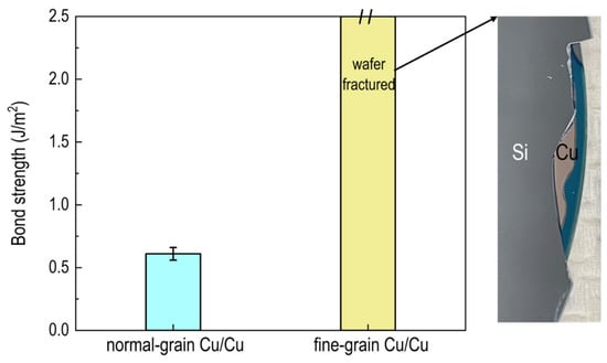
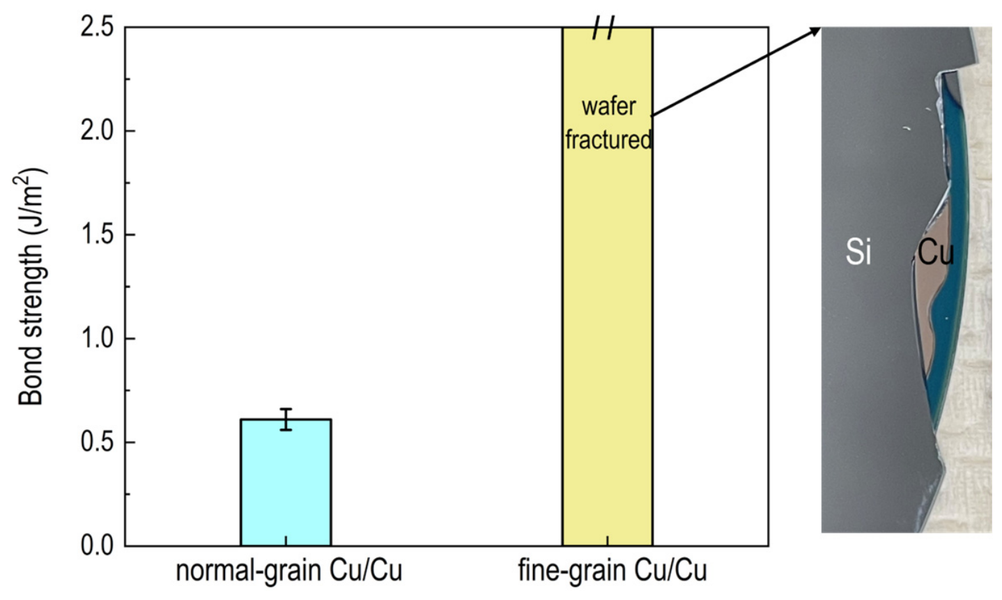
After being irradiated by an Ar ion beam and sequential plasma, normal-grain Cu and fine-grain Cu wafers were bonded in air. As shown in Figure 6 [33], the bond strength of normal-grain Cu/Cu wafers was approximately 0.6 J/m2. In contrast, the fine-grain Cu/Cu wafers fractured during testing, preventing the direct measurement of bond strength. This indicates that the bond strength exceeded the fracture strength of the wafer, suggesting strong interfacial bonding.
Figure 6.
Bond strength of normal-grain Cu/Cu and fine-grain Cu/Cu wafers.
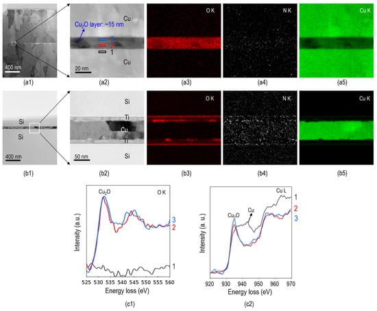
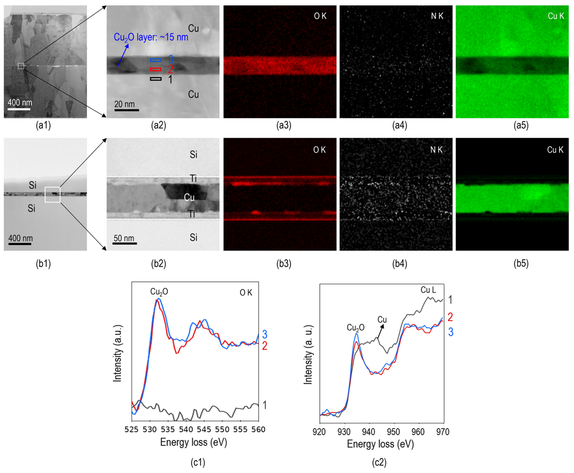
Figure 7 shows the cross-sectional STEM images, EDS mappings and EELS results of normal-grain and fine-grain Cu/Cu bonded interfaces. At the bonded interface of the normal-grain Cu/Cu wafers, an oxide layer with a thickness of ~15 nm was observed [33]. Based on the EELS results, the interfacial oxide was identified as Cu2O [34,35]. For the fine-grain sample, pronounced O signals were observed at the Si/Ti and Ti/Cu interfaces, whereas no obvious O enrichment was detected at the Cu/Cu bonded interface. The observed strong O signals are probably due to the native oxide on the Si surface and the strong oxygen affinity of Ti [36,37]. N was observed throughout the bonded region but no obvious enrichment at the bonded interface. A similar N signal distribution was found in a reference sample treated with an Ar ion beam and O2 plasma without N2 plasma (see Figure S1 in the Supplementary Material). These observations suggest that the O and N signals detected at the Cu/Cu bonded interface mainly originated from background signals rather than an interfacial oxide or nitride layer. The absence of O and N enrichment at the bonded interface may be related to the high density of grain boundaries in fine-grain Cu, which provided fast diffusion pathways for oxygen and nitrogen during post-annealing [38]. In addition, Cu grain growth was observed after annealing, and in some regions the original bonded interface was no longer distinguishable, indicating grain growth across the bonded plane [39]. Such microstructural evolution suggests the formation of direct Cu-Cu metallurgical bonding. Consistent with this observation, wafer fracture occurred during DCB testing of the fine-grain Cu/Cu wafers.
Figure 7.
Cross-sectional STEM images, EDS mappings and EELS results of normal-grain and fine-grain Cu/Cu wafers. (a1,a2) STEM image of normal-grain Cu/Cu wafers. (a3–a5) O, N and Cu mapping of (a2). (b1,b2) STEM image of fine-grain Cu/Cu wafers. (b3–b5) O, N and Cu mapping of (b2). (c1,c2) EELS of O K edges and Cu L edges for different points in (a2).
4. Conclusions
Cu/Cu wafer hydrophilic bonding at 200 °C was investigated. With sequential plasma activation, the effect of the bonding atmosphere on normal-grain Cu/Cu bonding was examined. For wafers bonded in air, the interfacial oxide layer was approximately 80 nm thick and consisted mainly of Cu2O. XPS results suggest that a small amount of CuO may also have been present. For wafers bonded under a vacuum of 1000 Pa, an approximately 10 nm thick Cu2O layer was observed. The bond strengths of both were close, and the bonding performed under vacuum tended to be stronger. With Ar ion beam treatment combined with sequential plasma activation, Cu wafers with different grain sizes were bonded in air. An approximately 15 nm thick Cu2O layer was observed at the normal-grain Cu/Cu bonded interface with a relatively low bond strength of 0.6 J/m2. In contrast, no oxide or nitride was detected at the fine-grain Cu/Cu bonded interface, and Cu grain growth across the interface occurred. Wafer fracture occurred during bond strength testing, indicating strong interfacial bonding.
Supplementary Materials
The following supporting information can be downloaded at https://www.mdpi.com/article/10.3390/mi17111348/s1. Figure S1: Cross-sectional STEM images and EDS mappings of fine-grain Cu/Cu wafers treated with Ar ion beam and O2 plasma. (a1) STEM image. (a2) N mapping of (a1); Table S1: Measured and theoretical d-spacings and inter-spot angles for the indexed FFT patterns in Figure 3; Table S2: Measured and theoretical d-spacings and inter-spot angles for the indexed FFT patterns in Figure 4.
Author Contributions
J.W. designed and carried out the experiments, analyzed the experimental results, and wrote the manuscript. J.W. and T.S. discussed all the results and commented on and edited the manuscript. K.T., M.K. (Michitaka Kubota), M.K. (Masaya Kawano), T.T., M.N. and T.K. discussed some of the results and commented on the manuscript. All authors have read and agreed to the published version of the manuscript.
Funding
This research was funded by the New Energy and Industrial Technology Development Organization (NEDO), Japan, grant number JPNP20017, and was also partly supported by the Precise Measurement Technology Promotion Foundation (PMTP-F).
Data Availability Statement
The datasets used and/or analyzed during the current study can be made available from the corresponding author upon reasonable request.
Acknowledgments
This article is a revised and expanded version of two conference papers: “Investigation of Low Temperature Cu/Cu Wafer Bonding for Hybrid Bonding Applications,” presented at the 8th International Workshop on Low-Temperature Bonding for 3D Integration (LTB-3D 2024), held in Nara, Japan, from 30 October to 1 November 2024 [28]; and “Low-Temperature Cu/Cu Wafer Bonding via SAB Combined with Sequential Plasma Activation,” presented at the 9th International Workshop on Low-Temperature Bonding for 3D Integration (LTB-3D 2026), held in Kanazawa, Japan, from 13 to 15 May 2026 [33].
Conflicts of Interest
The authors declare no conflicts of interest.
References
- Derakhshandeh, J.; De Preter, I.; Gerets, C.; Hou, L.; Heylen, N.; Beyne, E.; Beyer, G.; Slabbekoorn, J.; Dubey, V.; Jourdain, A.; et al. 3D stacking using bump-less process for sub 10 µm pitch interconnects. In Proceedings of the 2016 IEEE 66th Electronic Components and Technology Conference (ECTC), Las Vegas, NV, USA, 31 May–3 June 2016; pp. 128–133. [Google Scholar]
- Chew, S.A.; Zhang, B.; Vanstreels, K.; Chery, E.; De Messemaeker, J.; Witters, L.; Van Sever, K.; Iacovo, S.; Dewilde, S.; Stucchi, M.; et al. The challenges and solutions of Cu/SiCN wafer-to-wafer hybrid bonding scaling down to 400nm pitch. In Proceedings of the 2023 International Electron Devices Meeting (IEDM), San Francisco, CA, USA, 9–13 December 2023; pp. 1–4. [Google Scholar]
- Ma, K.; Bekiaris, N.; Hsu, C.H.; Xue, L.; Ramaswami, S.; Ding, T.; Probst, G.; Wernicke, T.; Uhrmann, T.; Wimplinger, M. 0.5 μm pitch wafer-to-wafer hybrid bonding at low temperatures with SiCN bond layer. In Proceedings of the 2024 IEEE 74th Electronic Components and Technology Conference (ECTC), Denver, CO, USA, 28–31 May 2024; pp. 331–336. [Google Scholar]
- Kim, Y.I.; Yang, K.H.; Lee, W.S. Thermal degradation of DRAM retention time: Characterization and improving techniques. In Proceedings of the 2004 IEEE International Reliability Physics Symposium, Phoenix, AZ, USA, 25–29 April 2004; pp. 667–668. [Google Scholar]
- Chang, M.; Lin, J.; Lai, C.S.; Chang, R.D.; Shih, S.N.; Wang, M.Y.; Lee, P.I. Si-H bond breaking induced retention degradation during packaging process of 256 Mbit DRAMs with negative wordline bias. IEEE Trans. Electron Devices 2005, 52, 484–491. [Google Scholar] [CrossRef]
- Kim, J.W.; Jeong, M.H.; Park, Y.B. Effect of HF & H2SO4 pretreatment on interfacial adhesion energy of Cu-Cu direct bonds. Microelectron. Eng. 2012, 89, 42–45. [Google Scholar] [CrossRef] [Scilit]
- Jang, E.J.; Hyun, S.; Lee, H.J.; Park, Y.B. Effect of wet pretreatment on interfacial adhesion energy of Cu-Cu thermocompression bond for 3D IC packages. J. Electron. Mater. 2009, 38, 2449–2454. [Google Scholar] [CrossRef] [Scilit]
- Hung, T.H.; Kang, T.C.; Mao, S.Y.; Chou, T.C.; Hu, H.W.; Chiu, H.Y.; Shih, C.L.; Chen, K.N. Investigation of wet pretreatment to improve Cu-Cu bonding for hybrid bonding applications. In Proceedings of the 2021 IEEE 71st Electronic Components and Technology Conference (ECTC), Virtual Conference, 1 June–4 July 2021; pp. 700–705. [Google Scholar]
- Yang, W.; Akaike, M.; Suga, T. Effect of formic acid vapor in situ treatment process on Cu low-temperature bonding. IEEE Trans. Compon. Packag. Manuf. Technol. 2014, 4, 951–956. [Google Scholar] [CrossRef] [Scilit]
- Jangam, S.; Bajwa, A.A.; Mogera, U.; Ambhore, P.; Colosimo, T.; Chylak, B.; Iyer, S. Fine-pitch (≤10 µm) direct Cu-Cu interconnects using in-situ formic acid vapor treatment. In Proceedings of the 2019 IEEE 69th Electronic Components and Technology Conference (ECTC), Las Vegas, NV, USA, 28–31 May 2019; pp. 620–627. [Google Scholar]
- Kim, T.H.; Howlader, M.M.R.; Itoh, T.; Suga, T. Room temperature Cu–Cu direct bonding using surface activated bonding method. J. Vac. Sci. Technol. A 2003, 21, 449–453. [Google Scholar] [CrossRef] [Scilit]
- Shigetou, A.; Itoh, T.; Matsuo, M.; Hayasaka, N.; Okumura, K.; Suga, T. Bumpless interconnect through ultrafine Cu electrodes by means of surface-activated bonding (SAB) method. IEEE Trans. Adv. Packag. 2006, 29, 218–226. [Google Scholar] [CrossRef] [Scilit]
- Takagi, H.; Utsumi, J.; Takahashi, M.; Maeda, R. Room-temperature bonding of oxide wafers by Ar-beam surface activation. ECS Trans. 2008, 16, 531–537. [Google Scholar] [CrossRef] [Scilit]
- Tan, C.S.; Lim, D.F.; Ang, X.F.; Wei, J.; Leong, K.C. Low temperature Cu-Cu thermo-compression bonding with temporary passivation of self-assembled monolayer and its bond strength enhancement. Microelectron. Reliab. 2012, 52, 321–324. [Google Scholar] [CrossRef] [Scilit]
- Lykova, M.; Panchenko, I.; Schneider-Ramelow, M.; Suga, T.; Mu, F.; Buschbeck, R. Cu-Cu thermocompression bonding with a self-assembled monolayer as oxidation protection for 3D/2.5D system integration. Micromachines 2023, 14, 1365. [Google Scholar] [CrossRef] [Scilit]
- Mariappan, M.; Mori, K.; Kurachi, A.; Imori, T.; Kojima, T.; Nakano, W.; Hashimoto, H.; Fukushima, T. Multi-functional self-assembled monolayer for chip-to-chip and chip-to-wafer hybrid bonding. In Proceedings of the 2024 IEEE 74th Electronic Components and Technology Conference (ECTC), Denver, CO, USA, 28–31 May 2024; pp. 45–50. [Google Scholar]
- Cheemalamarri, H.K.; Fujino, M.; Ghosh, T.; Umralkar, R.B.; BSS, C.R.; Singh, N.; Vempati, S.R. Void-free Cu/dielectric hybrid bonding at low-temperature enabled by ultrathin metal passivation engineering for 3D-IC applications. Commun. Eng. 2026, 5, 104. [Google Scholar] [CrossRef] [Scilit]
- Hsu, M.P.; Lin, T.Y.; Huang, H.J.; Wang, C.Y.; Chung, T.F.; Wu, W.W.; Chen, K.N. Thermal stability enhancement of low temperature Cu-Cu bonding using metal passivation technology for advanced electronic packaging. Commun. Eng. 2025, 4, 216. [Google Scholar] [CrossRef] [Scilit]
- Park, H.; Seo, H.; Kim, S.E. Anti-oxidant copper layer by remote mode N2 plasma for low temperature copper-copper bonding. Sci. Rep. 2020, 10, 21720. [Google Scholar] [CrossRef] [Scilit]
- Hu, L.; Goh, S.C.K.; Tao, J.; Lim, Y.D.; Zhao, P.; Lim, M.J.Z.; Salim, T.; Velayutham, U.M.; Tan, C.S. Time-dependent evolution study of Ar/N2 plasma-activated Cu surface for enabling two-step Cu-Cu direct bonding in a non-vacuum environment. ECS J. Solid State Sci. Technol. 2021, 10, 124001. [Google Scholar] [CrossRef] [Scilit]
- Park, H.; Seo, H.; Kim, Y.; Park, S.; Kim, S.E. Low-temperature (260 °C) solderless Cu–Cu bonding for fine-pitch 3-D packaging and heterogeneous integration. IEEE Trans. Compon. Packag. Manuf. Technol. 2021, 11, 565–572. [Google Scholar] [CrossRef] [Scilit]
- Lee, S.; Oh, G.; Choi, J.; Kim, Y.; Park, S.; Kim, S.E. Investigation of Cu-to-Cu and oxide-to-oxide bonding. In Proceedings of the 2023 IEEE 73rd Electronic Components and Technology Conference (ECTC), Orlando, FL, USA, 30 May–2 June 2023; pp. 1519–1523. [Google Scholar]
- Lee, Y.G.; McInerney, M.; Joo, Y.C.; Choi, I.S.; Kim, S.E. Copper bonding technology in heterogeneous integration. Electron. Mater. Lett. 2024, 20, 1–25. [Google Scholar] [CrossRef] [Scilit]
- Faure, M.; Dubarry, C.; Renaud, P.; Baudin, F.; Dominguez, S.; Abadie, K.; Morales, C.; Matei, C.; Fournel, F. Ultra low temperature hybrid bonding: Morphological and electrical characterizations. In Proceedings of the 2024 IEEE 10th Electronics System-Integration Technology Conference (ESTC), Berlin, Germany, 11–13 September 2024; pp. 1–6. [Google Scholar]
- Chen, Y.A.; Ong, J.J.; Tran, D.P.; Chiu, W.L.; Chang, H.H.; Hsu, W.Y.; Chen, C. Efficient Cu/SiO2 hybrid bonding through alkaline surface modification for 3D IC integration. Appl. Surf. Sci. 2025, 689, 162534. [Google Scholar] [CrossRef] [Scilit]
- Chen, Y.A.; Ong, J.J.; Chiu, W.L.; Hsu, W.Y.; Yang, S.C.; Chang, H.H.; Chen, C. Non-TCB process Cu/SiO2 hybrid bonding using plasma-free hydrophilicity enhancement with NaOH for chip-to-wafer bonding. In Proceedings of the 2024 IEEE 74th Electronic Components and Technology Conference (ECTC), Denver, CO, USA, 28–31 May 2024; pp. 399–403. [Google Scholar]
- Takeuchi, K.; Ninomiya, T.; Kubota, M.; Kawano, M.; Takagi, T.; Niwa, M.; Kuroda, T.; Suga, T. Hydrophilic bonding of SiO2/SiO2 and Cu/Cu using sequential plasma activation. ECS Trans. 2023, 112, 95–101. [Google Scholar] [CrossRef] [Scilit]
- Wang, J.; Takeuchi, K.; Ninomiya, T.; Kubota, M.; Kawano, M.; Takagi, T.; Niwa, M.; Kuroda, T.; Suga, T. Investigation of low temperature Cu/Cu wafer bonding for hybrid bonding applications. In Proceedings of the 2024 8th International Workshop on Low Temperature Bonding for 3D Integration (LTB-3D), Nara, Japan, 30 October–1 November 2024; p. 1. [Google Scholar]
- Maszara, W.P.; Goetz, G.; Caviglia, A.; McKitterick, J.B. Bonding of silicon wafers for silicon-on-insulator. J. Appl. Phys. 1988, 64, 4943–4950. [Google Scholar] [CrossRef] [Scilit]
- Fournel, F.; Continni, L.; Morales, C.; Da Fonseca, J.; Moriceau, H.; Rieutord, F.; Barthelemy, A.; Radu, I. Measurement of bonding energy in an anhydrous nitrogen atmosphere and its application to silicon direct bonding technology. J. Appl. Phys. 2012, 111, 104907. [Google Scholar] [CrossRef] [Scilit]
- Thermo Fisher Scientific. Copper. Available online: https://www.thermofisher.com/us/en/home/materials-science/learning-center/periodic-table/transition-metal/copper.html (accessed on 15 October 2026).
- Lee, S.Y.; Mettlach, N.; Nguyen, N.; Sun, Y.M.; White, J.M. Copper oxide reduction through vacuum annealing. Appl. Surf. Sci. 2003, 206, 102–109. [Google Scholar] [CrossRef] [Scilit]
- Wang, J.; Takeuchi, K.; Kubota, M.; Kawano, M.; Takagi, T.; Niwa, M.; Kuroda, T.; Suga, T. Low-temperature Cu/Cu wafer bonding via SAB combined with sequential plasma activation. In Proceedings of the 2026 9th International Workshop on Low Temperature Bonding for 3D Integration (LTB-3D), Kanazawa, Japan, 13–15 May 2026; p. 1. [Google Scholar]
- Wang, Y.; Lany, S.; Ghanbaja, J.; Fagot-Revurat, Y.; Chen, Y.P.; Soldera, F.; Horwat, D.; Mücklich, F.; Pierson, J.F. Electronic structures of Cu2O, Cu4O3, and CuO: A joint experimental and theoretical study. Phys. Rev. B 2016, 94, 245418. [Google Scholar] [CrossRef] [Scilit]
- Keast, V.J. Application of EELS in materials science. Mater. Charact. 2012, 73, 1–7. [Google Scholar] [CrossRef] [Scilit]
- Butz, R.; Rubloff, G.W.; Ho, P.S. Chemical bonding and reactions at Ti/Si and Ti/oxygen/Si interfaces. J. Vac. Sci. Technol. A 1983, 1, 771–775. [Google Scholar] [CrossRef] [Scilit]
- Laurila, T.; Zeng, K.; Kivilahti, J.K.; Molarius, J.; Suni, I. Effect of oxygen on the reactions in the Si/Ta/Cu metallization system. J. Mater. Res. 2001, 16, 2939–2946. [Google Scholar] [CrossRef] [Scilit]
- Fang, Y.; Wang, Y.; Bian, Y.; Ngiam, Y.; Huang, M.X. Enhancing oxidation resistance of Cu thin film through grain size reduction. Acta Mater. 2026, 302, 121676. [Google Scholar] [CrossRef] [Scilit]
- He, C.; Zhou, J.; Zhou, R.; Chen, C.; Jing, S.; Mu, K.; Huang, Y.T.; Chung, C.C.; Cherng, S.J.; Lu, Y.; et al. Nanocrystalline copper for direct copper-to-copper bonding with improved cross-interface formation at low thermal budget. Nat. Commun. 2024, 15, 7095. [Google Scholar] [CrossRef] [Scilit]
Disclaimer/Publisher’s Note: The statements, opinions and data contained in all publications are solely those of the individual author(s) and contributor(s) and not of MDPI and/or the editor(s). MDPI and/or the editor(s) disclaim responsibility for any injury to people or property resulting from any ideas, methods, instructions or products referred to in the content. |
© 2026 by the authors. Licensee MDPI, Basel, Switzerland. This article is an open access article distributed under the terms and conditions of the Creative Commons Attribution (CC BY) license.