


Abstract
This paper proposes a single-stage common-ground series-capacitor-compensated buck–boost inverter (CG-SCC-BBI) for wide-input DC–AC applications. Featuring a common-ground neutral and a series-blocking film capacitor, the topology inherently suppresses high-frequency common-mode leakage-current excitation and blocks the structural DC offset. To counteract frequency-dependent voltage attenuation caused by the output network, a fundamental-frequency equivalent model is derived to pre-scale the modulation reference and fully restore output voltage amplitude. The four-switch power stage operates with single-active-leg PWM, confining high-frequency switching to a single half-bridge at any instant to significantly reduce the switching-loss budget. Furthermore, by eliminating the conventional line-frequency output filter choke and utilizing film capacitors exclusively, the topology completely avoids electrolytic capacitors, thereby enhancing long-term operational reliability and lifespan. The proposed inverter supports seamless transition between boost and buck operating modes across the entire input-voltage range. Its operating principles are validated through time-domain simulations, and these were experimentally verified on a 300 W SiC MOSFET standalone laboratory prototype. Experimental results confirm correct operation from 95 V to 400 V DC input, achieving maximum measured efficiencies of 96.79% at the rated 300 W under low-input operation and 97.66% at the rated 300 W under high-input operation, while maintaining an output-current total harmonic distortion (THD) below 2.5%.
1. Introduction
Over the last two decades, renewable-energy sources and distributed DC power systems have become increasingly important for residential and commercial electricity applications [1]. In these systems, low-power single-phase DC–AC inverters, typically rated below 1 kW, constitute the key power-conditioning stage that converts a variable DC source into a regulated AC supply for diverse AC power systems and standalone loads [2,3,4]. A fundamental challenge in many DC-powered AC conversion systems is the wide variation in input voltage, which may originate from renewable-energy sources, battery-storage systems, or other variable DC supplies. Ratios exceeding 2:1 between the minimum and the maximum operating voltage are common in such sources [1,2]. Conventional full-bridge voltage-source inverters (VSIs) are intrinsically buck converters whose AC output amplitude cannot exceed the DC-bus voltage, leaving them unable to exploit the full operating range of a wide-range DC source. This constraint motivates the search for single-phase inverter topologies with intrinsic voltage-boosting capability [3].
A well-established route to buck–boost inversion cascades a front-end boost DC–DC converter with a conventional VSI, forming a two-stage conversion chain [2]. While this architecture separates front-end voltage conditioning from DC–AC conversion, it requires an additional energy-storage inductor and a bulk interstage capacitor and subjects the power to two successive conversion events, each introducing switching and conduction losses [5,6]. The resulting system is larger, costlier, and less efficient than an equivalent single-stage design. These penalties have driven extensive research into single-stage topologies that provide voltage boosting and AC synthesis within one power-processing stage [2,5].
Several single-stage buck–boost families, surveyed comprehensively in [7], eliminate the two-stage cascade penalty. The Z-source inverter [5] exploits the otherwise-forbidden shoot-through state to boost the DC link, but at the cost of significant device current stress and a carefully designed impedance network. Switched-boost [8] and diode-assisted [9] inverters reduce the passive count at the expense of an additional active switch. Split-inductor differential-boost topology [10] achieves single-stage buck–boost through bimodal operation, yet suffers circulating-current paths that complicate control and reduce high-gain efficiency. The quasi-switched-boost inverter [11] references its output to the positive DC rail to suppress common-mode swings, but it is restricted to boost-only mode and cannot synthesize output voltages below the DC input. Differential and electrolytic-capacitor-less buck–boost families originally developed for wide-input-voltage power-conditioning applications [12,13] broaden this design space further, yet each retains either a large magnetic count or a boost-only gain characteristic.
A significant milestone in single-stage buck–boost conversion is the three-phase GaN Y-inverter reported by Antivachis et al. [14], which delivers high-quality sinusoidal output over a wide DC range through a compact four-switch-per-phase topology at high switching frequency. A return-path-inductor variant [15] further reduces device current stress while extending the input range, and related three-phase architectures based on coupled inductors [6] and Z-source networks [16] have also been reported to have high-performance power conversion. Their common-mode behavior has been systematically reviewed in [17]. However, all of these topologies are inherently three-phase, requiring three independent LC filter sets and three coordinated modulation channels, making them less suitable for compact single-phase AC power systems, where reduced hardware complexity, lower cost, and high power density are primary design objectives. Developing a single-phase inverter that preserves the wide-input-voltage capability and compact switching architecture of the Y-inverter family while operating from a conventional two-terminal AC output therefore remains an important research challenge.
In transformerless single-phase inverters, common-mode (CM) leakage current remains an important design concern because high-frequency variations of the common-mode voltage (CMV) across parasitic capacitances may generate unwanted leakage current, electromagnetic interference, and additional system losses [18,19,20]. Galvanic isolation effectively suppresses this phenomenon, but increases converter size, weight, and cost [21]. Among transformerless solutions, the H6 [21] and HERIC [22] topologies reduce leakage current by decoupling the DC and AC sides during the zero state, while improved modulation and clamping techniques further suppress the residual leakage current [23,24]. Nevertheless, these converters cannot completely eliminate the leakage associated with device parasitic capacitances, and NPC- and T-type converters [25] require a split DC-link structure that increases capacitor count and hardware complexity. Comparative studies of transformerless single-phase and multilevel inverter topologies have reached similar conclusions [26]. However, these existing topologies generally remain limited to either buck or boost operation or require additional power-conversion stages, making it difficult to simultaneously achieve wide-input-voltage operation, compact structure, and common-ground capability within a single-stage inverter.
An elegant way to suppress leakage current is the common-ground (CG) inverter, in which one terminal of the DC source is permanently bonded to the AC neutral so that the CMV is clamped to a constant value by design rather than by modulation. The traditional CG family introduced by Siwakoti and Blaabjerg [27] establishes this principle with a low component count, but its members operate in buck mode only and therefore inherit the limited-voltage-range drawback of the conventional VSI. To add boosting, a second class of topologies references the AC output to the positive DC rail (V+) by tying the output neutral to the source positive terminal. Huang et al. [28] realize a four-switch CG inverter with dual-mode (buck–boost/buck) operation and a DC-link requirement only slightly higher than the required AC output amplitude; however, its asymmetric per-half-cycle operation produces uneven thermal stress and requires floating gate drivers. Boost-oriented positive-rail designs built from standard half-bridge modules [29], systematically derived single-stage boost families [30], and single-source nine-level boost inverters with a low switch count [31]—together with the more recent common-ground stages built from four [32] and five [33] switches—further raise the voltage gain and output quality, yet they remain confined to boost-only operation and demand high duty cycles that elevate inductor current and switch voltage stress. Across this evolution, a single-phase positive-rail topology that simultaneously delivers true buck-and-boost gain and inherent leakage elimination is still missing.
Because positive-rail power stages generate a unipolar intermediate voltage containing both a DC offset and the desired AC component, a series-blocking film capacitor Cs is inserted between the power stage and the load to remove the offset before delivery. Nguyen and Tran [34] adopt exactly this principle in a four-switch single-stage switched-boost inverter, where a series DC-blocking capacitor isolates the offset at the output. While conceptually simple, this capacitor carries the full AC load current, so its equivalent series resistance raises conduction losses at high load. Moreover, that work cannot recover the load-dependent voltage attenuation the capacitor introduces. The same reactive impedance appears in positive-rail topologies that reference the output to V+ [11,28] and in virtual-ground buck–boost inverters that clamp the reference node through an auxiliary branch [35,36], yet these either operate in a single gain mode, rely solely on an outer regulator, or omit a physically motivated compensation model. To the best of the authors’ knowledge, no reported single-phase common-ground inverter simultaneously provides genuine buck–boost capability together with an analytically derived model that compensates for the voltage attenuation introduced by the mandatory series-blocking capacitor.
To bridge this gap, this paper proposes the CG-SCC-BBI topology for wide-input DC–AC power conditioning. By employing a model-based compensation that pre-adjusts the modulation reference based on the known load, the proposed system turns the reactive attenuation of the blocking network into a precisely managed design parameter. The specific contributions are as follows. (1) The proposed topology permanently bonds the AC neutral to the positive terminal of the DC source, inherently fixing the common-mode voltage and eliminating high-frequency leakage current without relying on modulation techniques, while a series-blocking film capacitor isolates the structural DC offset. (2) Unlike traditional inverters, the proposed topology requires no bulky output filter inductor, achieving high-quality output voltage filtering using only a single parallel capacitor, which significantly reduces the system’s total volume, weight, and hardware cost. (3) A steady-state analytical model rigorously characterizes the frequency-dependent voltage-divider effect among the series capacitor, output capacitor, and load. Based on this model, a straightforward open-loop compensation scales the modulation reference beforehand to compensate for the voltage drop without requiring output-voltage feedback. (4) Practical component-selection guidelines are established for the energy-storage inductor, intermediate buffer capacitor, series-blocking capacitor, and output capacitor based on boundary-conduction operation, capacitor-ripple, and voltage-retention criteria.
2. The Proposed CG-SCC-BBI
2.1. Circuit Topology and Operating Principle
The proposed CG-SCC-BBI is a single-phase, non-isolated, single-stage buck–boost topology that synthesizes an AC output from a DC source without a bulky, lossy isolation transformer. As illustrated in Figure 1, it integrates two functional blocks: a four-switch buck–boost power stage and a passive three-element output-coupling network. To establish an unambiguous framework for steady-state analysis, four circuit nodes are designated throughout. Node “a” is the primary switching node, where the midpoint of the boost half-bridge, the intermediate capacitor Cp, and the series-blocking capacitor Cs meet. Node “b” is the negative terminal (V−) of the DC input source. Node “o” is the active terminal of the AC output, formed at the junction of Cs, the output filter capacitor Co, and the load. Node “n” is the AC output neutral. With this convention, the three core element voltages are written compactly as the internode potentials:
where vab is the unipolar node “a” potential referred to the negative DC rail, vao is the instantaneous voltage across the series-blocking capacitor, and von is the inverter AC output voltage vo across the filter capacitor Co. Referred to the output neutral, the total synthesized output-side voltage is van = va − vn = vCs + vo, which comprises a DC offset Van,DC and a sinusoidal AC component van,AC.
Figure 1.
Proposed common-ground non-isolated buck–boost inverter: (a) complete topology with labeled nodes a, b, o, n; (b) buck-regime interval with S3 and S1 conducting; (c) boost-regime interval with S4 and S1 conducting; (d) buck-regime freewheeling interval with S3 and S2 conducting.
The power stage uses four active switches, S1–S4, arranged as two complementary half-bridge legs. The upper (buck) half-bridge is formed by S1 and S2, with its midpoint tied to one terminal of the energy-storage inductor L1. The lower (boost) half-bridge consists of S3 and S4, whose midpoint forms the primary switching node “a”. Bridging node “a” and the negative rail, the intermediate capacitor Cp acts purely as a local energy buffer and high-frequency ripple filter for the switching cell. As a high-frequency decoupling element, it carries no fundamental-frequency load current and plays no role in the output model of Section 3.
A defining feature of this topology is the placement of the AC output neutral “n”. Rather than referencing it to the negative DC rail as in conventional systems, it is permanently bonded to the positive rail (V+) of the input source. This direct bonding establishes a true common-ground topology that clamps the common-mode voltage to a constant value independently of high-frequency switching, suppressing parasitic ground leakage current at its origin.
The resulting structural DC offset is isolated from the load by the three-element coupling network. Specifically, the series-blocking film capacitor Cs, inserted between node “a” and output terminal “o,” withstands the DC bias so that only the fundamental AC component is delivered downstream. The output filter capacitor Co, connected in parallel with the load between nodes “o” and “n,” attenuates high-frequency switching harmonics to ensure output waveform quality and a transformerless single-phase power-processing cell.
2.2. Topological Switching States
Within each high-frequency switching period, the converter operates in one of two regimes—buck or boost—depending on whether the instantaneous target output voltage is lower or higher than the input voltage Vin. In both regimes, high-frequency pulse-width modulation (PWM) is confined to a single half-bridge leg while the other leg is clamped, which limits the switching-loss budget relative to a conventional four-switch full-bridge inverter.
Buck regime (Vo ≤ Vin). The left half-bridge is clamped by keeping S3 permanently ON and S4 OFF. High-frequency switching is executed entirely by the right half-bridge (S1 and S2). When S1 is ON (Figure 1b), the inductor L1 is connected between node “a” (via S3) and the neutral node “n” (via S1), and energy is transferred through the reactive network. When S1 turns OFF (Figure 1d), S2 provides a freewheeling path and the inductor current circulates through S3, L1, and S2 back to node “b,” releasing stored energy to the intermediate capacitor Cp.
Boost regime (Vo > Vin). The right half-bridge is clamped by holding S1 permanently ON and S2 OFF. High-frequency modulation is transferred to the left half-bridge (S3 and S4). When S4 is ON (Figure 1c), the inductor L1 is connected between node “b” and node “n” (the positive rail via S1), so the source energizes L1 and its current ramps up. When S4 turns OFF, S3 turns ON and steers the inductor current into node “a,” boosting the potential across Cp and driving energy through Cs to the load.
Because high-frequency commutation is confined to a single leg at any instant, the circuit operates as an integrated single-stage non-inverting buck–boost cell with a seamless buck-to-boost transition. Crucial to the modeling in Section 3, the series capacitor Cs is the only series element between node “a” and output node “o,” forcing the total load current io to flow through it across all switching states. Consequently, the fundamental load current induces a notable reactive voltage drop across Cs, directly shaping the output voltage delivered to the load.
3. Mathematical Modeling of Series-Capacitor and Output-Voltage Interdependence
This section derives the fundamental-frequency amplitude attenuation and phase shift imposed by the series coupling network.
3.1. Fundamental-Frequency Equivalent Circuit
To analyze the steady-state behavior at the fundamental line frequency (ωo), the superposition principle is applied to decouple the DC and AC components. Because the intermediate capacitor Cp operates entirely within the switching cell to buffer high-frequency switching ripples, it carries no fundamental load current. Consequently, the fundamental-frequency output model simplifies to the series-blocking capacitor Cs, the output filter capacitor Co, and the load.
The modulation employs a unipolar reference voltage at node “a,” va(t) = Va,pk (sin ωo t + 1), whose amplitude is denoted by Va,pk. Its implementation is described in Section 4. Under the adopted carrier-based strategy, the carrier-averaged voltage across Cp follows this reference in both the buck and the boost regime, so its average DC value over one fundamental period is VCp,DC = Va,pk.
Referring to the AC output neutral “n”—which is permanently bonded to the positive DC rail (Vin)—the structural DC offset voltage Van,DC is derived as:
and Cs, being a capacitor, blocks this offset, so that VCs,DC = Van,DC, no DC current reaches the load, and only the AC component van,AC(t) = Va,pk sin ωot is delivered.
At the fundamental frequency the filter-capacitor current and the resistive load current are related by |ICo|/|IR| = ωo Co R = R/XCo. With Co = 6.8 µF and fo = 60 Hz, XCo ≈ 390 Ω, so this ratio reaches approximately 1.03 at the 400 Ω light-load condition of Table 1, where the filter-capacitor current slightly exceeds the resistive-load current. The output branch is therefore represented by the parallel combination:
fed through the series-blocking capacitor of impedance:
with XCs ≈ 12.06 Ω for Cs = 220 µF.
Table 1.
Fundamental-frequency model quantities and the error introduced by neglecting Co (Cs = 220 µF, Co = 6.8 µF, fo = 60 Hz, Vo = 110 Vrms).
3.2. Voltage-Transfer Function and Voltage-Retention Factor
Apply the voltage divider formed by Equations (3) and (4):
The first denominator term, 1 + Co/Cs, is the load-independent capacitive divider between Cs and Co, and the second, XCs/R, is the reactive drop across Cs and vanishes as the load is lightened. The magnitude of Equation (5) gives the voltage-retention factor and the uncompensated output voltage:
and the angle by which the load voltage leads the synthesized source:
which is governed by the sum Cs + Co rather than by Cs alone. At no load does the attenuation vanish:
which equals 0.970 for the prototype. This load-independent residue bounds the open-circuit output, so the modulator never has to synthesize an unbounded reference. Figure 2 plots kv against Cs from Equation (6). Each curve saturates at the ceiling given by Equation (8) rather than at unity.
Figure 2.
Voltage-retention factor kv of Equation (6) versus the series-blocking capacitance Cs (Co = 6.8 µF, fo = 60 Hz) for the three load conditions of Table 1. The dotted curve is the load-independent no-load ceiling of Equation (8), which the retention factor approaches as the load is lightened.
3.3. Series-Capacitor Current, Voltage, and Sensitivity to the Filter Capacitance
The current forced through Cs is the sum of the resistive and the capacitive branch currents:
and the fundamental voltage it develops across the series capacitor is:
Setting Co = 0 in (6) gives the first-order approximation:
whose relative error, together with the output-voltage deficit incurred when the gain kcomp,0 = 1/kv,0 is used in place of kcomp = 1/kv, is:
Table 1 evaluates Equations (6)–(12) over the complete operating range for Cs = 220 µF, Co = 6.8 µF, and fo = 60 Hz.
The error stays between 2.8% and 3.1% and grows as the load is lightened, because the load-independent divider of Equation (8) becomes the dominant attenuation mechanism once the reactive drop across Cs has decayed. At 400 Ω, the filter-capacitor current, 0.282 A irrespective of load, exceeds the resistive one and raises ICs,rms by 43% above Vo/R. Since the compensation is open-loop and no feedback path removes a residual gain error, the full model—Equations (5)–(10)—is used for the compensation law of Section 4 and for the component stresses of Section 5.
4. Modulation and Model-Based Voltage Compensation
The modulation strategy uses the factor kv of Equation (6) to pre-adjust its reference so that the target output is obtained for the known load. This section presents the DC-offset scheme that guarantees a unipolar reference, the dual duty-cycle generation, the model-based compensation, and the operating limits and load sensitivity that the compensation implies.
4.1. DC-Offset Sinusoidal Modulation
A non-inverting buck–boost converter cannot produce a negative node “a” voltage, so a plain sinusoidal reference is unrealizable. Adding a DC offset equal to the peak output voltage gives node “a” reference to the negative rail:
where Vo is the target RMS output voltage, ωo = 2πfo, and the unity offset ensures va(t) ≥ 0 for all t. Referred to the output neutral, this equals the synthesized voltage van(t) = va(t) − Vin analyzed in Section 3, where Va,pk denotes the peak value of the AC component of the node “a” reference and equals √2Vo before compensation. The peak of the unipolar node “a” potential itself is therefore Va,max = 2Va,pk. The normalized modulation index and its span are:
4.2. Dual Duty-Cycle Control Law Derivation
At each sampling instant, the controller computes ma(t), selects the operating state, and forms the dual duty cycles for the two switch pairs. In the buck state (ma < 1), the upper half-bridge (S1 and S2) chops while S3 is clamped ON and S4 OFF, so dα1 = ma(t) and dα2 = 1. Averaging the switched node over one carrier period gives:
In the boost state (ma ≥ 1), the lower half-bridge (S3 and S4) chops while S1 is clamped ON and S2 OFF. Volt-second balance on L1 over one switching period, with D4 = 1 − dα2 the fraction for which S4 conducts, gives:
so that dα1 = 1 and dα2 = 1/ma(t). Equations (15) and (16) also justify Equation (2), since in both states the carrier-averaged node voltage equals the reference. Collecting both states, the dual duty-cycle control law executed by the modulator is:
Gate signals G1 and G2 are complementary and so are G3 and G4, so only one switch pair switches at high frequency at any instant, which reduces the switching-loss budget relative to full-bridge operation. The boundary ma = 1 is crossed twice per fundamental period, at:
which has a solution only for 0 ≤ Vin ≤ 2Va,pk. Above that, the converter stays in the buck regime over the whole period. These relationships are illustrated in Figure 3.
Figure 3.
Modulation waveforms illustrating the buck-to-boost transition and dual duty-cycle generation.
4.3. Model-Based Compensation of the Series-Capacitor Voltage Drop
Because Equation (6) gives kv in closed form for the known Cs, Co, and R, the reference is scaled before operation by the compensation factor:
so that the compensated reference and its amplitude become:
Substituting this amplitude into Equation (6) gives:
that is, the target output is restored exactly, because by construction kcomp = 1/kv. The compensated modulation index is:
and Equation (17) applies unchanged, with ma replaced by ma,comp.
Since the proposed compensation is open-loop, the compensation factor is calculated only once for each intended operating condition and stored in the digital signal processor (DSP) as a constant coefficient. Three values, listed in Table 2, cover the 10–100% load range of the prototype. No online estimation, adaptive update or output-voltage measurement is performed during operation. Note also that Equation (19) contains no Vin, so a given load resistance yields the same kcomp at every input voltage. The input voltage acts only on the modulation index through Equation (22), and hence on the buck or boost regime.
Table 2.
Series-blocking capacitance sizing at the two tested load conditions (Vin = 95 V, ma,lim = 4).
4.4. Operating Limits and Load Sensitivity
Because the reference amplitude in Equation (20) is scaled by kcomp, so is the modulation index. The peak value reached by Equation (22) is:
which supersedes the uncompensated limit of Equation (14): the maximum modulation index does include the compensation scaling. Its realizable upper bound is not ma = 1, since the converter is deliberately operated with ma > 1 throughout the boost regime, but the smallest boost duty ratio dα2,min = 1/ma,lim that the modulator can produce, which is set by the dead time and the minimum switch on-time at fs. Hence:
A conservative controller-imposed minimum duty ratio dα2,min = 0.25 is adopted for the prototype to leave sufficient margin for digital pulse resolution, transient operation, parasitic voltage drops, and current ripple. This constraint is not dictated by the converter topology itself, but is selected as a conservative control limit that guarantees adequate PWM pulse width at the 50 kHz switching frequency within the resolution of the digital signal processor. This choice yields ma,lim = 4, corresponding to a minimum allowable input voltage of Vin,min = 83.5 V at full load, whereas the experimental operating point Vin = 95 V operates at ma,pk = 3.52.
The accuracy of an open-loop gain depends on how closely the actual load matches the design value. Differentiating Equation (19) gives the normalized sensitivity:
For the prototype (Cs = 220 μF, fo = 60 Hz, XCs = 12.06 Ω), the normalized sensitivity equals −0.0788 at the rated (40 Ω) and −0.0009 at the light-load (400 Ω) condition, respectively. Therefore, if the actual load resistance differs from the design value by ±10%, the resulting steady-state output-voltage deviation remains below 0.8%.
Since the proposed compensation is purely open-loop, the compensation factor remains unchanged during load transients until a new coefficient is selected. Consequently, temporary steady-state voltage deviations may appear under abrupt load changes. If tighter voltage regulation is required, Equation (19) can be incorporated as the feedforward term of a conventional outer voltage-control loop.
5. Design Guidelines
The component values follow from the steady-state model of Section 3 and Section 4. Each criterion is expressed in closed form and evaluated for the prototype in Table 2 and Table 3.
Table 3.
Compensation factor and compensated peak modulation index (23) versus input voltage (Vo = 110 Vrms); kcomp is independent of Vin.
5.1. Energy-Storage Inductor
The inductor L1 is dimensioned to limit the high-frequency ripple to a fraction γ of the maximum inductor current. In the boost regime, which governs that maximum:
where D4 is largest at the peak of the reference. Imposing ΔiL1 ≤ γIL1,max gives:
The maximum inductor current is not obtained from a closed-form estimate, because the instantaneous power of a single-phase stage pulsates at twice the line frequency and the conduction intervals depend on the duty ratio. It is instead taken as the largest time-domain value over the operating range.
5.2. Intermediate Capacitor
The intermediate capacitor Cp buffers the boost half-bridge and attenuates the high-frequency ripple at node “a”. It is sized to keep ΔvCp within 1–2% of the maximum node voltage Va,max of Equation (30):
A polypropylene or ceramic capacitor with a low equivalent series resistance (ESR) is recommended. With the switching-cell passives fixed, the remaining degree of freedom is the series-blocking capacitance, which sets the retention factor and hence the compensation gain.
5.3. Series-Blocking Capacitor
The series-blocking capacitor is the most critical passive component: through Equations (6) and (19), it sets the retention factor and the compensation gain, and through Equation (32) its own voltage rating. It influences Equation (6) through two distinct parameters: the load-independent capacitive-divider ratio Co/Cs and the load-dependent reactive term XCs/R. Consequently, the two attenuation mechanisms respond differently to a change in capacitance: at the prototype ratio Cs/Co ≈ 32, a further 10% increase in capacitance improves kv by 0.95% at full load, but by only 0.28% at light load where the fixed divider dominates. Beyond this point, the volume and cost penalties outweigh the marginal gain.
A lower bound on Cs follows directly from the modulation limit in Equation (24). Substituting the largest admissible compensation factor into Equation (19) yields a quadratic equation in 1/Cs whose positive root is:
5.4. Operating Region and Input-Voltage Range
The admissible input-voltage range is bounded below by Equation (24) and unbounded above: for Vin ≥ 2Va,pk. The reference never crosses the input level and the converter operates purely in the buck region. Table 3 evaluates Equation (23) for two load conditions at the minimum (95 V) and maximum (400 V) input voltages considered in Section 6.
The compensation factor kcomp depends solely on the output network and is independent of Vin, whereas the compensated peak modulation index ma,pk decreases as Vin increases. Consequently, the 95 V case requires mixed buck–boost operation (ma,pk > 1), whereas the 400 V case operates entirely in the buck region (ma,pk < 1).
All entries satisfy Equation (24) with ma,lim = 4. The resulting compensated reference amplitude Va,pk serves as the baseline for deriving all device voltage and current stresses.
5.5. Component Voltage and Current Stress
The compensation raises the synthesized reference by kcomp, so every voltage stress derived from the node ”a” potential scales accordingly. From Equation (20):
The upper half-bridge is clamped to Vin under all conditions, whereas S3 and S4 are tied to the switching node “a”:
Equation (30) gives 334.2 V at full load and 320.9 V at light load for Va,max, against the 311.1 V predicted by the uncompensated expression 2√2Vo. The compensated values agree with the peak of approximately 331 V observed in Section 6, confirming that the kcomp scaling must be retained in the device rating. The blocking stress on S3 falls to zero during buck operation, where it is clamped permanently ON. The series capacitor must withstand the DC bias of Equation (2) plus the peak of Equation (10):
which yields 119.2 V at full load and 72.2 V at light load for Vin = 95 V, so a film capacitor rated to roughly twice VCs,max provides adequate margin. The RMS current of a device is set by its own conduction interval:
where gk(t) is the conduction function of Sk, equal to unity while the device conducts and zero otherwise. Because the conduction intervals are set by the operating regime, the most heavily loaded device changes with the input voltage: S1 under low-input-voltage operation and S3 under pure-buck operation. The individual device RMS currents used in the loss calculation are therefore extracted from the time-domain switching waveforms. Since Equations (6), (19), (29), and (30) depend only on the passive output-network parameters and the target output, the same procedure scales directly to other power ratings and output voltages.
6. Simulation and Experimental Results
6.1. Validation of the Analytical Model by Simulation
The proposed CG-SCC-BBI and its model-based compensation were verified by time-domain simulation in PLECS, covering both boost and buck operation to confirm the full buck–boost capability. The power stage operates at a switching frequency of fs = 50 kHz with a 250 ns dead time to synthesize a 60 Hz, 110 Vrms AC output. To evaluate parameter sensitivity and validate the operating limits predicted by Equations (24) and (29), two series capacitance values were tested: the nominal design value (Cs = 220 μF) and a halved capacitance (Cs = 110 μF). Furthermore, testing under two distinct DC input voltages—95 V for low-input-voltage operation and 400 V for high-input-voltage, pure-buck operation—demonstrates the wide-input capabilities of the converter. The evaluation spans the full operating power range from 10% (30 W, R = 400 Ω) to 100% (300 W, R = 40 Ω) of the rated load. All simulation waveforms were recorded from t = 0.4 s to 0.5 s to ensure that steady-state conditions were reached. The simulation parameters are summarized in Table 4, matching those of the experimental prototype in Section 6.2 for direct consistency.
Table 4.
Simulation and prototype parameters.
6.1.1. Steady-State Operation at Low Input Voltage
At Cs = 220 μF, the compensated reference from Equation (20) successfully maintains the output close to the 110 Vrms target across both load conditions. Figure 4 illustrates the full-load operation (300 W) at Vin = 95 V, where the output is a clean 108.6 Vrms sinusoid. As required by Equation (13), the node ”a” voltage remains strictly non-negative throughout the fundamental period, while the series capacitor carries a positive DC bias of VCs,DC = 72.1 V, consistent with Equations (2) and (20). The switch-stress profile in Figure 5 is dictated by the topology rather than the load: S1 and S2 are clamped to the 95 V input, whereas S3 and S4 block approximately 331 V.
Figure 4.
Full-load steady-state waveforms at low input voltage (300 W, Vin = 95 V, Cs = 220 µF): (a) voltages vo, va, vCp, vCs; (b) currents iL1, iR, iCs.
Figure 5.
Switch voltage-stress waveforms at low input voltage (300 W, Vin = 95 V, Cs = 220 µF).
Figure 6 repeats this test at 30 W light load using the same reference law, adjusting only kcomp, which directly confirms Equation (9) in the time domain. Here, the total current forced through Cs is 0.394 Arms, whereas the resistive load branch draws only Vo/R = 0.275 Arms. The remaining 0.282 Arms represents the current through the filter capacitor Co. Because this filter current is load-independent, it becomes dominant as the load lightens. This behavior clearly demonstrates why omitting Co from the compensation model is untenable: a phenomenon masked at 300 W full load where the same 0.282 A constitutes less than 10% of the resistive load current.
Figure 6.
Light-load steady-state waveforms at low input voltage (30 W, 10% of rated power, Vin = 95 V, Cs = 220 µF): (a) voltages; (b) currents.
6.1.2. Steady-State Operation at High Input Voltage
Raising the input voltage to 400 V while maintaining the same 110 Vrms target demonstrates the converter’s buck capability, confirming true buck–boost operation alongside the low-input results. Figure 7 illustrates the inverter stepping 400 V down to 110 Vrms. From Equation (23), the peak modulation index is ma,pk = 0.835. Since ma,pk < 1 throughout the fundamental period, the boundary condition Equation (18) has no solution, and hence the converter never enters the boost region and operates with dα2 = 1 continuously. The corresponding switch voltage-stress profiles under high input voltage are presented in Figure 8.
Figure 7.
Full-load steady-state waveforms at high input voltage (300 W, Vin = 400 V, Cs = 220 µF): (a) voltages; (b) currents.
Figure 8.
Switch voltage-stress waveforms at high input voltage (300 W, Vin = 400 V, Cs = 220 µF).
Varying Vin introduces two fundamental operating changes predicted by the steady-state model in Section 3: As Vin increases, the DC bias across Cs (VCs,DC = √2 kcomp Vo-Vin) reverses polarity, shifting from +72.1 V at Vin = 95 V to −232.9 V at Vin = 400 V. Because the fundamental AC voltage across Cs remains constant at 33.3 Vrms, the peak voltage stress VCs,max reaches its worst-case maximum (280.1 V) during high-input buck operation, establishing Vin = 400 V as the critical design point for dimensioning Cs. At low input voltage (Vin = 95 V), S3 and S4 withstand the peak node “a” potential of 334 V, while S1 and S2 are clamped to the 95 V DC rail. Conversely, at high input voltage (Vin = 400 V), S1 and S2 execute high-frequency PWM and block the full 400 V DC bus, whereas S4 withstands the peak node “a” potential (334 V) and S3 remains clamped permanently ON with virtually zero blocking stress.
Figure 9 completes the experimental matrix under the light-load condition (30 W) at high input voltage. The output voltage is held at 109.9 Vrms using the same compensation coefficient as at 95 V. The series-capacitor DC bias settles at −240.0 V with a fundamental AC ripple of 4.74 Vrms, closely matching the values predicted by Equations (2) and (10). Figure 10 shows the corresponding light-load switch stress waveforms.
Figure 9.
Light-load steady-state waveforms at high input voltage (30 W, 10% of rated power, Vin = 400 V, Cs = 220 µF): (a) voltages; (b) currents.
Figure 10.
Simulated switch voltage-stress waveforms at the light-load condition (30 W, Cs = 220 µF): (a) Vin = 95 V; (b) Vin = 400 V.
6.1.3. Verification of the Voltage-Retention Factor and of the Compensation Law
The primary objective of the simulation was to quantitatively verify the voltage-retention factor derived in Equation (6) and the model-based compensation strategy proposed in Equation (19). From the simulated output RMS voltage Vo,sim, the realized retention factor kv,sim is extracted as:
and the corresponding residual voltage-regulation error εV is defined as:
where Vo = 110 Vrms is the target of Equation (13) and kcomp the coefficient of Equation (19) evaluated for the load under test. Table 5 compares Equation (34) with the analytical value Equation (6).
Table 5.
Analytical prediction versus simulation of the output-network model and of the compensated output voltage (Cs = 220 µF).
Table 5 compares the analytical predictions with the simulation results across all four extreme operating corners (full/light load under 95 V and 400 V inputs). The circuit-level retention factor kv,sim agrees with the analytical value kv from Equation (6) to within 1.3%, while the residual output-regulation error εV stays well below 1.31% in all tested cases.
The minor deviation observed at Vin = 95 V (−1.31% at full load and −1.03% at light load) stems primarily from the higher current stress inherent to boost operation. At low input voltage, the converter processes significantly higher inductor and switch currents, which magnify the fundamental-frequency voltage ripple across the energy-buffer capacitors (Cp and Cs) and induce slight parasitic conduction drops across the power stage. Conversely, at Vin = 400 V, the system operates entirely in the buck regime with substantially lower operating currents, minimizing these secondary effects and improving the analytical-to-simulation agreement to +0.18% and −0.14%.
6.1.4. Component Voltage and Current Evaluation
Table 6 compares the analytically predicted component-voltage stresses with the simulation results at the four operating corners. These points cover the minimum and maximum input voltages as well as 10% and 100% of rated power. The analytical predictions agree closely with the simulation results, confirming that the revised model provides sufficiently accurate estimates for semiconductor and capacitor voltage ratings. In particular, the model correctly predicts the polarity reversal of the series-capacitor dc bias between the 95 V and 400 V operating conditions. The small discrepancies are mainly attributed to switching ripple, dead time, and nonideal circuit elements included in the simulation.
Table 6.
Component voltage stress: analytical prediction versus simulation at the four operating corners (Cs = 220 µF).
Table 7 summarizes the RMS currents of the energy-storage inductor and the power switches at the rated output power (300 W) under the two extreme input-voltage conditions. At 95 V, the energy-storage inductor and switch S1 carry the highest RMS currents because the converter operates in the buck–boost mode with a large input current. At 400 V, the higher input voltage leads to a substantial reduction in the input current, resulting in lower RMS currents in L1 and S1. In this pure buck operating regime, S3 conducts the main inductor current, while the current through S4 becomes negligible.. These results provide useful guidance for component current ratings and thermal design.
Table 7.
Simulated RMS currents of the energy-storage inductor and of the power switches at the rated output power of 300 W under low- and high-input-voltage operation.
6.1.5. Sensitivity to Series Capacitance
To evaluate the parameter robustness of the proposed model-based compensation and validate the theoretical lower capacitance bound Cs,min derived in Equation (29), a deliberate parameter mismatch scenario was simulated. The series capacitance Cs was halved to 110 μF while the open-loop compensation factor kcomp was held fixed at the nominal 220 μF design value. This tests the ability of the analytical expression Equation (6) to accurately predict off-design system performance under uncompensated impedance variations.
Table 8 compares the analytically predicted output voltages with the circuit simulation results, and Figure 11 overlays the corresponding output voltage waveforms at full load (300 W) for both Vin = 95 V and Vin = 400 V.
Table 8.
Output voltage when Cs is halved to 110 µF while kcomp is held at its 220 µF value.
Figure 11.
Output-voltage comparison at 300 W for Cs = 220 µF and Cs = 110 µF, with the compensation factor fixed at its 220 µF value: (a) Vin = 95 V; (b) Vin = 400 V.
The simulation results agree with the analytical predictions derived from Equation (6) to within 0.42 V across both input voltage extremes. Halving Cs increases the uncompensated series reactance XCs, resulting in an output voltage drop of approximately 12.4% at 95 V (96.38 Vrms) and 11.7% at 400 V (97.10 Vrms). The close agreement with the predicted value of 96.8 Vrms quantitatively confirms the accuracy of the retention model in Equation (6) under off-design operating conditions.
Furthermore, as illustrated in Figure 11, the output voltage maintains a clean sinusoidal waveform without harmonic degradation, which shows that a parameter mismatch produces purely an amplitude regulation error rather than waveform distortion. It should be emphasized that the 110 µF case is not a compensated design evaluated at the theoretical boundary, because kcomp is deliberately retained at its nominal 220 µF value. It is a 50% parameter-mismatch test. Recomputing the coefficient for Cs = 110 µF would give kcomp ≈ 1.221 and would restore the 110 Vrms target, at the cost of a compensated peak modulation index approaching the limit set by Equation (24). This is the practical significance of Cs,min, and it is why a nominal 220 µF is selected for the prototype: the resulting factor-of-two margin absorbs component manufacturing tolerances and ageing while keeping the required compensation gain far from the modulation limit.
6.1.6. Operation with a Nonlinear Load
Rectifier-fed equipment represents a common load class for standalone AC supplies, drawing current in short pulses near the peak of the output voltage. To evaluate performance under nonlinear loading, the converter was simulated with the circuit shown in Figure 12, comprising a single-phase diode-bridge rectifier, a 560 μF smoothing capacitor, and an 80 Ω load resistor. Because the series-blocking capacitor Cs carries the full pulsed rectifier current, this configuration imposes the most demanding steady-state operating condition on the coupling network analyzed in Section 3.
Figure 12.
Nonlinear load configuration: a single-phase diode-bridge rectifier with a capacitive filter (C = 560 µF) and a resistive load (R = 80 Ω).
Figure 13 and Figure 14 present the steady-state waveforms under low-input and high-input conditions. In both cases, the output voltage exhibits the flat-topped waveform characteristic of capacitive rectifier loads, yielding RMS values of 107.6 V and 103.4 V while delivering 216 W and 204 W to the DC load, respectively. The rectified DC output voltage settles at 131.6 V (95 V input) and 127.7 V (400 V input) with a double-line-frequency ripple of approximately 14 V, while the load resistor draws continuous currents of 1.64 A and 1.60 A. Driven by the pulsed current, the voltage across Cs experiences peak-to-peak excursions of 71 V and 69 V, both well within the film capacitor ratings established in Section 5.5.
Figure 13.
Simulated steady-state waveforms with the nonlinear load under low-input-voltage operation (Vin = 95 V, C = 560 µF, R = 80 Ω): output voltage vo, series-capacitor voltage vCs, rectifier output voltage VR, and load current iR.
Figure 14.
Simulated steady-state waveforms with the nonlinear load under high-input-voltage operation (Vin = 400 V, C = 560 µF, R = 80 Ω): output voltage vo, series-capacitor voltage vCs, rectifier output voltage VR, and load current iR.
These results confirm that the converter maintains stability under nonlinear loads. The residual output RMS deviations (−2.2% at 95 V and −6.0% at 400 V relative to the 110 Vrms target) occur because the open-loop compensation factor is calculated from a resistive fundamental-frequency equivalent rather than the complex nonlinear input impedance. To fully restore the target voltage amplitude under such loads, either the equivalent fundamental resistance at the delivered active power must be substituted into Equation (3), or the open-loop compensation factor should serve as the feedforward term in an outer closed-loop voltage controller.
6.2. Experimental Validation
A laboratory prototype was constructed and evaluated to verify the analysis experimentally (Figure 15). The power stage uses C2M0080120D SiC MOSFETs (1200 V, 36 A, 80 mΩ, Wolfspeed, Durham, NC, USA) switching at 50 kHz. The energy-storage inductor L1 has a nominal value of 250 µH with a measured ESR of 0.11 Ω. WCAP-FTBE film capacitors (6.8 µF, 400 V, Würth Elektronik, Waldenburg, Germany) are used for both the intermediate capacitor Cp and the output filter capacitor Co for their low ESR, and the series-blocking capacitor Cs is implemented as two PILKOR PCPW-245 film capacitors (110 µF, 450 V, PILKOR Electronics, Ansan, Republic of Korea) in parallel for an effective 220 µF. The remaining parameters are those of Table 4.
Figure 15.
Experimental laboratory prototype of the proposed CG-SCC-BBI.
To evaluate performance across the 10–100% power range (40 Ω to 400 Ω), open-loop compensation scaling factors derived from Equation (19) were preloaded into the DSP. Under full-load operation (300 W), the prototype maintains precise output voltage regulation in both operating regimes using the fixed open-loop compensation. Under low-input-voltage operation (Vin = 95 V), the measured output voltage reaches 109.5 Vrms, representing a minor deviation of −0.45% relative to the 110 Vrms target. Under high-input-voltage operation (Vin = 400 V), the output voltage settles at 111.7 Vrms, corresponding to a residual regulation error of +1.55%. These residual positive biases stem from component manufacturing tolerances (film capacitors and load resistors), finite DSP reference resolution, and sensor calibration accuracy, remaining well within the sensitivity limits predicted in Section 6.2.10.
6.2.1. Steady-State Operation at Low Input Voltage
Figure 16 illustrates the experimental steady-state performance at the rated output power of 300 W under low input voltage conditions. By applying the model-based voltage compensation factor derived from the analytical parameters and validated in simulation, the prototype synthesizes a clean sinusoidal output voltage of 109.5 Vrms. The small voltage error relative to the 110 Vrms target confirms both the single-stage voltage-boosting capability and the effectiveness of the proposed compensation scheme in counteracting the voltage drop across the series capacitor.
Figure 16.
Experimental steady-state waveforms under full load at low input voltage (300 W, Vin = 95 V): (a) vo, iL1, vCp, vCs; (b) vo, vCp; (c) vS1, vS2, iR; (d) vS3, iin, vS4.
Regarding semiconductor stress, the off-state voltage across S1 and S2 is clamped at the 95 V input, confirming that high-frequency PWM switching is confined to a single half-bridge leg. S3 and S4 block the peak potential at node “a,” which aligns with the theoretical stress model presented in Section 5.
The measured displacement between the fundamental components of the output voltage vo and the node potential vCp is approximately 13.4° compared with the 16.3° predicted by Equation (7) for an ideal network at full load. This small discrepancy is accounted for by the parasitic ESR of the capacitor bank and the winding resistance of inductor L1, which introduce a resistive component to the series branch and reduce the reactive angle. Nevertheless, the empirical load trend remains entirely consistent with the model: as the load resistance R increases and the reactance-to-resistance ratio XCs/R decays, the phase displacement collapses to 1.7° at high resistance levels.
6.2.2. Steady-State Operation at High Input Voltage
Experimental verification of pure-buck operation (Vin = 400 V) at rated power is shown in Figure 17, matching the simulation setup in Section 6.1.2. The inverter maintains a stable sinusoidal output with S3 clamped fully ON while high-frequency PWM is executed exclusively by S1 and S2, validating the predicted switching sequence, voltage-stress distribution, and wide-input-voltage capability.
Figure 17.
Experimental steady-state waveforms under full load at high input voltage (300 W, Vin = 400 V), where the converter remains in the buck region throughout the fundamental period: (a) vo, iL1, vCp, vCs; (b) vo, vCp; (c) vS1, vS2, iR; (d) vS3, iin, vS4.
Figure 17 also confirms the predicted DC-bias polarity reversal across Cs: as Vin exceeds the peak compensated output voltage, VCs transitions from positive to negative bias while its fundamental AC voltage ripple remains constant. These measured waveforms directly validate the theoretical model.
6.2.3. Steady-State Operation Under Light-Load Condition
Figure 18 compares the experimental steady-state waveforms at 30 W, corresponding to 10% of the rated output power, for Vin = 95 V and Vin = 400 V. In both cases, the inverter maintains a stable sinusoidal output voltage. Because the load current is small, the fundamental-frequency voltage variation across the series capacitor Cs is also reduced. Consequently, the phase difference between the output voltage vo and the intermediate-node voltage vCp becomes less pronounced than at rated load. The measured dc bias of Cs also follows the predicted operating behavior: it is positive at Vin = 95 V and negative at Vin = 400 V.
Figure 18.
Experimental steady-state waveforms at the light-load condition (30 W, R = 400 Ω, 10% of rated power): (a) low input voltage; (b) high input voltage.
6.2.4. Operation with a Reactive Load
To verify system performance under a reactive load, an inductive RL load with R = 40 Ω and L = 30 mH was applied as shown in Figure 19, introducing a distinct phase shift between the voltages across the inductor (vL) and the resistor (vR). Despite this, vR preserves its high-quality sinusoidal profile. Furthermore, vCs and vL exhibit stable steady-state waveforms, confirming stable operation of the proposed topology under a non-resistive load. The compensation coefficient used in this test remains based on the nominal resistive-load model. Extending the analytical compensation to a general complex load requires the load resistance in Equation (3) to be replaced by the corresponding load impedance, which changes both kv and the phase angle of Equation (7).
Figure 19.
Experimental steady-state waveforms with an inductive (RL) load (R = 40 Ω, L = 30 mH): series-capacitor voltage vCs, load current iR, load-resistor voltage vR and inductor voltage vL.
6.2.5. Operation with a Nonlinear Load
To evaluate performance under nonlinear loading, a single-phase diode-bridge rectifier with a 560 μF DC-link capacitor and an 80 Ω DC load was connected to the inverter output (Figure 20). Despite the high-crest-factor pulsed current drawn by the rectifier, the inverter operates stably, preserving its output-voltage envelope with the typical flat-topping characteristics associated with capacitor-input rectifier loads.
Figure 20.
Experimental waveforms feeding a single-phase diode-bridge rectifier with a 560 µF DC-link capacitor and a resistive DC load: output voltage vo, output current io and rectified DC-link voltage.
6.2.6. Load-Step Transients
Figure 21 illustrates the transient performance during an abrupt transition from no-load to full-load conditions under both low and high input voltages. With the compensation coefficient held fixed at its full-load value throughout the step, the test evaluates open-loop stability under an unannounced load change. The inverter exhibits a seamless dynamic response, settling rapidly to steady state without overshoot, ringing, or mode-transition instability. The slight voltage shift observed before the step corresponds to the difference between the no-load and full-load voltage-retention factors, as predicted by Equations (6) and (8).
Figure 21.
Experimental transient waveforms during the transition from no load to rated load: (a) low input voltage; (b) high input voltage.
Figure 22 further evaluates open-loop behavior during a load step from 100 Ω (121 W) to 50 Ω (242 W) while retaining the initial 100 Ω compensation factor. As expected for an unadjusted feedforward scheme, doubling the load current introduces a minor, predictable steady-state voltage drop (−2.0% deviation, yielding 107.8 Vrms). Nevertheless, the output voltage settles quickly without severe transient overshoot or sustained oscillation, governed by the passive output network. These results confirm that the open-loop compensation scheme remains inherently stable under severe load steps, producing a bounded and calculable regulation error that can be eliminated by updating the compensation gain.
Figure 22.
Experimental output behavior during a load step from 100 Ω (121 W) to 50 Ω (242 W): (a) vo, iL1; (b) vo, iR.
6.2.7. Output-Current Harmonic Content
To evaluate the output power quality, the output-current THD was analyzed across the operating load range at the low input voltage Vin = 95 V. Table 9 summarizes the measured and simulated THD values together with the relative, error defined as:
Table 9.
Experimental and simulated output-current THD versus output power, with the relative deviation of Equation (36).
The experimental THD remains slightly higher than the simulated value, with an absolute difference of approximately 0.04–0.05 percentage points and a relative deviation εTHD of 1.7–5.6%. The small discrepancy is mainly attributed to practical nonidealities not fully represented in the simulation, including semiconductor voltage drops, passive-component parasitics, interconnection effects, and uncertainty in the current-probe and FFT measurements. Nevertheless, both the simulated and experimental THD values remain below 2.5% over the measured load range.
Table 10 presents the simulated output-current harmonic components at rated power under the two extreme input-voltage conditions. At Vin = 95 V, the second-order harmonic is dominant at 2.24%, followed by the third-order harmonic at 0.74%, while the fifth- to eleventh-order harmonics remain below 0.05% of the fundamental. At Vin = 400 V, all reported low-order harmonics remain below 0.03%, indicating substantially lower current distortion in pure-buck operation.
Table 10.
Simulated output-current harmonic magnitudes normalized to the fundamental at rated power (%).
6.2.8. Common-Mode Voltage and Leakage Current
Figure 23 presents the measured common-mode voltage (vCM) and ground leakage current (ilk) across an emulated parasitic capacitance connected between the negative DC rail and earth, in accordance with the test procedure commonly adopted for common-ground topologies [31,33]. Because the AC output neutral is directly bonded to the positive DC rail, high-frequency common-mode voltage fluctuations across the parasitic capacitance are structurally eliminated, confining vCM to a DC offset with a minor low-frequency component.
Figure 23.
Measured common-mode voltage vCM and leakage current ilk through an emulated parasitic capacitance: (a) low input voltage; (b) high input voltage.
Consequently, the measured RMS leakage current is 38 mA under low input voltage (Vin = 95 V) and 25 mA under high input voltage (Vin = 400 V). These values correspond to only 12.7% and 8.3% of the 300 mA safety threshold dictated by the DIN VDE 0126-1-1 standard [37], respectively. These experimental results confirm that the common-ground structure effectively suppresses common-mode leakage current well within regulatory safety limits while maintaining stable sinusoidal output operation.
6.2.9. Loss Breakdown and Efficiency
To analyze power-dissipation mechanisms and evaluate switching-loss reduction, a comprehensive loss model was developed using device datasheet parameters for the C2M0080120D SiC MOSFETs. Semiconductor dissipation includes RDS(on)-based conduction losses and switching losses derived from turn-on/turn-off energy profiles. Passive losses encompass inductor copper losses from the measured L1 ESR, core losses, and capacitor conduction losses from the equivalent series resistances of Cp, Cs, and Co. Table 11 details the resulting loss breakdown and calculated efficiency across four power levels under both input voltage regimes.
Table 11.
Computed loss breakdown (W) and simulated efficiency at both input voltages.
Figure 24 illustrates the loss breakdown versus output power at low input voltage, Vin = 95V. At the rated 300 W load, MOSFET conduction loss (6.16 W) and inductor loss (6.18 W) constitute 90.6% of the total power dissipation (13.62 W), whereas switching loss accounts for only 8.1% (1.10 W). Scaling power from 30 W to 300 W causes conduction and copper losses to increase quadratically. In contrast, switching loss increases only fivefold because high-frequency PWM commutation is confined to a single half-bridge leg. This confirms that full-load efficiency reduction is driven predominantly by conduction dissipation rather than switching penalties, validating the low switching-loss characteristic of the single-active-leg modulation strategy.
Figure 24.
Computed loss breakdown versus output power at low input voltage: MOSFET conduction, MOSFET switching, inductor (copper plus core) and capacitor ESR losses.
Figure 25 compares the loss distribution between input voltage extremes at rated power. At Vin = 400 V, total power loss drops significantly to 4.18 W (98.62% efficiency) compared to 13.62 W (95.66%) at 95 V. This efficiency improvement stems from a fourfold reduction in inductor and device RMS currents at elevated input voltage. Consequently, minimizing semiconductor RDS(on) and inductor winding resistance represents the primary path for further efficiency optimization and power scaling.
Figure 25.
Distribution of the total loss among the circuit components at the rated output power of 300 W: (a) Vin = 95 V, 13.62 W total; (b) Vin = 400 V, 4.18 W total.
Figure 26 compares the measured and calculated converter efficiency across the entire load range (30–300 W, corresponding to 10–100% of the rated power) under both input-voltage conditions. At Vin = 95 V, the measured efficiency reaches a maximum of 96.79% at 100 W and gradually decreases to 94.41% at the rated output power of 300 W. The experimental efficiency closely follows the analytical prediction, with the measured values remaining approximately one percentage point lower over the entire operating range. This difference is mainly attributed to practical nonidealities that are not fully represented in the analytical model, including semiconductor switching and conduction losses, passive-component parasitics, and parameter tolerances.
Figure 26.
Measured and simulated efficiency versus output power over the 10–100% load range at low and high input voltage.
6.2.10. Measurement Uncertainty and Parameter Sensitivity
To evaluate the repeatability of the experimental results, statistical processing was performed using five consecutive measurements for each operating condition. Table 12 summarizes the sample size, mean values, standard deviations, and instrument accuracies for the key performance parameters at the rated output power of 300 W. The low standard deviations confirm good measurement repeatability, while the remaining differences between the analytical, simulated, and experimental results are consistent with the practical nonidealities discussed in the preceding sections.
Table 12.
Statistical evaluation of the measured performance at the rated output power of 300 W (five consecutive trials per operating condition).
6.3. Thermal Behavior and Long-Term Reliability
Table 11 also provides the basis for the thermal assessment. At the rated operating point (300 W, Vin = 95V), the calculated total losses are 7.26 W in the four SiC MOSFETs and 6.18 W in the inductor. Using the specified thermal resistances, the worst-case junction-temperature rise is approximately 14 °C above ambient, indicating that all semiconductor devices operate with a comfortable margin below their 150 °C junction-temperature rating. The inductor therefore represents the dominant thermal design constraint. As device temperature increases, the SiC MOSFET on-state resistance and the inductor copper resistance also increase, leading to a moderate reduction in efficiency. Under a 100 °C temperature rise, the calculated efficiency decreases from 95.66% to approximately 94.3%, while the voltage-transfer relationships derived in Section 3 remain unaffected because they depend only on the passive-network parameters.
Regarding long-term reliability, the proposed converter employs only polypropylene film capacitors, eliminating the electrolyte dry-out mechanism associated with electrolytic capacitors. The sensitivity analysis in Section 5.3 shows that a 5% capacitance reduction produces less than a 0.5% change in the open-loop output voltage, indicating good tolerance to capacitor ageing. A comprehensive lifetime evaluation based on accelerated thermal-cycling and endurance testing is beyond the scope of this work and is left for future study.
6.4. Discussion on Power Scaling and Prospects
The design methodology presented in Section 5 is not restricted to the 300 W prototype. Because the voltage-retention factor and compensation characteristics are determined by the output-network parameters, the same design procedure can be applied to higher power ratings by appropriately selecting the passive components according to the scaling relationships established in Section 5. Similar buck–boost converter cells have been reported in multi-kilowatt applications, supporting the applicability of the underlying operating principle [38].
Three practical approaches may be considered for higher-power implementations. The first is interleaving multiple converter cells, which reduces the current stress of each phase, improves ripple cancellation, and facilitates thermal management. The second is increasing the switching frequency to reduce the required inductance and capacitance, thereby improving power density when wide-bandgap semiconductor devices are employed. The third is increasing the series capacitance Cs, which increases the voltage-retention factor, reduces the required compensation gain, and improves the operating margin over a wide input-voltage range. The appropriate scaling strategy depends on the target power level, efficiency, thermal constraints, and passive-component size.
For higher-power single-phase applications, the inherent twice-line-frequency power pulsation at the DC port should also be considered. This issue can be mitigated by incorporating an active power-decoupling circuit without modifying the proposed modulation strategy or compensation method [39,40,41]. In addition, previous studies have shown that smooth transition between the buck and boost operating modes requires appropriate coordination by the outer voltage controller under dynamic operating conditions [42]. Experimental validation of kilowatt-level prototypes and long-term reliability evaluation remain subjects for future work.
7. Comparative Evaluation
Table 13 compares the proposed converter with representative single-phase transformerless topologies, including buck-only common-ground inverters, boost inverters, and single-stage buck–boost converters. The comparison considers the semiconductor count, passive components, presence of a dedicated output filter inductor, input-voltage capability, common-ground implementation, and reported maximum efficiency.
Table 13.
Comparison of representative inverter topologies.
Since buck-only inverters cannot generate the required AC voltage from low input voltages, the H6 topology [21] and the traditional common-ground inverter [27] are additionally listed together with a front-end boost stage to provide an input-voltage capability comparable to that of the proposed converter.
The comparison highlights the trade-offs among the three topology families. Buck-only common-ground converters, such as the H6 topology [21] and the traditional common-ground inverter [27], achieve very high inverter efficiencies. However, their operating range is limited by the input voltage, and a front-end boost converter becomes necessary when a wide DC-input range is required. Although the additional boost stage extends the operating range, it also increases the number of semiconductor devices, passive components, and overall conversion stages, reducing the achievable system efficiency.
Single-stage boost-capable converters avoid the need for a front-end DC–DC converter, but generally require additional circuit complexity. The split-inductor differential boost inverter [10] employs multiple magnetic components, while the nine-level boost inverter [31] relies on a significantly larger number of active switches and capacitors. Other boost-capable topologies, including the half-bridge boost inverter [29] and the virtual-ground buck–boost inverter [35], reduce the number of magnetic components, but require five or more active switches. The dual-mode common-ground buck–boost inverter [28] achieves a four-switch configuration, although it relies on asymmetric modulation and floating gate drivers. The switched-boost topology in [34] also employs four switches, but incorporates additional passive components and does not include a compensation mechanism for the series-capacitor voltage drop.
Compared with these representative topologies, the proposed converter combines a wide input-voltage range of 95–400 V with a single-stage four-switch structure requiring no external diodes. It also eliminates the dedicated output filter inductor while maintaining common-ground operation throughout the entire operating range. The only magnetic component is the energy-storage inductor used for buck–boost power conversion, rather than a line-frequency output filter choke. Consequently, the proposed topology achieves a reduced semiconductor count while maintaining a measured peak efficiency of 96.79%.
Overall, the proposed converter does not aim to maximize inverter-only efficiency, as achieved by buck-only common-ground structures. Instead, it provides a balanced compromise among wide-input-voltage capability, reduced component count, common-ground operation, elimination of the dedicated output filter inductor, and competitive efficiency within a single-stage architecture. These characteristics make it particularly suitable for standalone power-conversion systems supplied by wide-range DC sources.
8. Conclusions
This paper presented the CG-SCC-BBI, a single-stage non-isolated buck–boost inverter for wide-input DC applications. The proposed topology combines common-ground operation, a series-blocking capacitor, and a model-based compensation method to achieve wide-range voltage conversion while eliminating the dedicated output filter inductor. It also employs only four active switches and no external diodes, resulting in a simple single-stage power-conversion structure.
A fundamental-frequency analytical model including the output capacitor was developed to predict the voltage-retention factor, component stresses, and operating limits. Based on this model, closed-form design guidelines were derived for the passive components and the modulation range. The analysis was verified by simulation and experimentally validated using a 300 W SiC MOSFET prototype under resistive, inductive, nonlinear, and transient operating conditions. The prototype achieved measured peak efficiencies of 96.79% at Vin = 95 V and 97.66% at Vin = 400 V, while maintaining an output-current THD below 2.5%.
The proposed converter represents a practical compromise between wide-input-voltage capability, common-ground operation, reduced semiconductor count, and competitive efficiency. Nevertheless, the present implementation employs an open-loop compensation method, exchanges the twice-line-frequency power ripple directly with the DC source, and has not yet been validated through long-term thermal-cycling or endurance testing. Future work will therefore focus on adaptive closed-loop voltage regulation, active power decoupling, and experimental validation of higher-power prototypes together with long-term reliability evaluation.
Author Contributions
Conceptualization, methodology, and writing—original draft, D.-V.V., Y.-C.L. and J.-H.C.; writing—review and editing, K.M.N. and J.-H.C.; software and simulation validation, V.-C.B.; hardware implementation and experimental validation, C.C.; supervision and resources, Y.-C.L.; funding acquisition, project administration, and resources, J.-H.C. All authors have read and agreed to the published version of the manuscript.
Funding
This work was supported by the National Research Foundation of Korea, funded by the South Korean government (MSIT) under grant RS-2023-00249376.
Data Availability Statement
The data presented in this study are available on request from the corresponding author.
Conflicts of Interest
The authors declare no conflicts of interest.
References
- Dhara, S.; Somasekhar, V.T. A Three-Phase Semi-Single Stage PV Inverter with Voltage Boosting and Leakage Current Minimization. IEEE Trans. Circuits Syst. II Express Briefs 2022, 69, 169–173. [Google Scholar] [CrossRef] [Scilit]
- Ho, C.N.M.; Siu, K.K.M. Manitoba Inverter—Single-Phase Single-Stage Buck-Boost VSI Topology. IEEE Trans. Power Electron. 2019, 34, 3445–3456. [Google Scholar] [CrossRef] [Scilit]
- Reddivari, R.; Jena, D. A Negative Embedded Differential Mode Γ-Source Inverter with Reduced Switching Spikes. IEEE Trans. Circuits Syst. II Express Briefs 2020, 67, 2009–2013. [Google Scholar] [CrossRef] [Scilit]
- Kibria, M.F.; Elsanabary, A.; Tey, K.S.; Mubin, M.; Mekhilef, S. A Comparative Review on Single Phase Transformerless Inverter Topologies for Grid-Connected Photovoltaic Systems. Energies 2023, 16, 1363. [Google Scholar] [CrossRef] [Scilit]
- Peng, F.Z. Z-Source Inverter. IEEE Trans. Ind. Appl. 2003, 39, 504–510. [Google Scholar] [CrossRef] [Scilit]
- Zhou, Y.; Huang, W.; Zhao, P.; Zhao, J. A Transformerless Grid-Connected Photovoltaic System Based on the Coupled Inductor Single-Stage Boost Three-Phase Inverter. IEEE Trans. Power Electron. 2014, 29, 1041–1046. [Google Scholar] [CrossRef] [Scilit]
- Azizi, M.; Husev, O.; Vinnikov, D. Single-Stage Buck–Boost Inverters: A State-of-the-Art Survey. Energies 2022, 15, 1622. [Google Scholar] [CrossRef] [Scilit]
- Ravindranath, A.; Mishra, S.K.; Joshi, A. Analysis and PWM Control of Switched Boost Inverter. IEEE Trans. Ind. Electron. 2013, 60, 5593–5602. [Google Scholar] [CrossRef] [Scilit]
- Gao, F.; Loh, P.C.; Teodorescu, R.; Blaabjerg, F. Diode-Assisted Buck–Boost Voltage-Source Inverters. IEEE Trans. Power Electron. 2009, 24, 2057–2064. [Google Scholar] [CrossRef] [Scilit]
- Khan, A.A.; Lu, Y.W.; Eberle, W.; Wang, L.; Khan, U.A.; Cha, H. Single-Phase Split-Inductor Differential Boost Inverters. IEEE Trans. Power Electron. 2020, 35, 107–120. [Google Scholar] [CrossRef] [Scilit]
- Nguyen, M.-K.; Le, T.-V.; Park, S.-J.; Lim, Y.-C. A Class of Quasi-Switched Boost Inverters. IEEE Trans. Ind. Electron. 2015, 62, 1526–1536. [Google Scholar] [CrossRef] [Scilit]
- Zhao, B.; Abramovitz, A.; Liu, C.; Yang, Y.; Huangfu, Y. A Family of Single-Stage, Buck-Boost Inverters for Photovoltaic Applications. Energies 2020, 13, 1675. [Google Scholar] [CrossRef] [Scilit]
- Choi, Y.-O.; Nguyen, K.M. Novel Single-Stage Electrolytic Capacitor-Less Buck-Boost Inverter. Energies 2024, 17, 6191. [Google Scholar] [CrossRef] [Scilit]
- Antivachis, M.; Kleynhans, N.; Kolar, J.W. Three-Phase Sinusoidal Output Buck-Boost GaN Y-Inverter for Advanced Variable Speed AC Drives. IEEE J. Emerg. Sel. Top. Power Electron. 2022, 10, 3459–3476. [Google Scholar] [CrossRef] [Scilit]
- Menzi, D.; Huber, J.E.; Kappeler, L.; Zulauf, G.; Kolar, J.W. New Return Path Inductor Buck–Boost Y-Inverter Motor Drive with Reduced Current Stresses. IEEE Trans. Power Electron. 2022, 37, 10086–10090. [Google Scholar] [CrossRef] [Scilit]
- Huang, Y.; Shen, M.; Peng, F.Z.; Wang, J. Z-Source Inverter for Residential Photovoltaic Systems. IEEE Trans. Power Electron. 2006, 21, 1776–1782. [Google Scholar] [CrossRef] [Scilit]
- Duong, T.-D.; Nguyen, M.-K.; Tran, T.-T.; Vo, D.-V.; Lim, Y.-C.; Choi, J.-H. Topology Review of Three-Phase Two-Level Transformerless Photovoltaic Inverters for Common-Mode Voltage Reduction. Energies 2022, 15, 3106. [Google Scholar] [CrossRef] [Scilit]
- Li, W.; Gu, Y.; Luo, H.; Cui, W.; He, X.; Xia, C. Topology Review and Derivation Methodology of Single-Phase Transformerless Photovoltaic Inverters for Leakage Current Suppression. IEEE Trans. Ind. Electron. 2015, 62, 4537–4551. [Google Scholar] [CrossRef] [Scilit]
- Lopez, O.; Teodorescu, R.; Freijedo, F.; Doval-Gandoy, J. Eliminating Ground Current in a Transformerless Photovoltaic Application. In Proceedings of the 2007 IEEE Power Engineering Society General Meeting, Tampa, FL, USA, 24–28 June 2007; IEEE: New York, NY, USA, 2007; pp. 1–5. [Google Scholar]
- Xiao, H.; Xie, S.; Chen, Y.; Huang, R. An Optimized Transformerless Photovoltaic Grid-Connected Inverter. IEEE Trans. Ind. Electron. 2011, 58, 1887–1895. [Google Scholar] [CrossRef] [Scilit]
- Zhang, L.; Sun, K.; Xing, Y.; Xing, M. H6 Transformerless Full-Bridge PV Grid-Tied Inverters. IEEE Trans. Power Electron. 2014, 29, 1229–1238. [Google Scholar] [CrossRef] [Scilit]
- Kerekes, T.; Teodorescu, R.; Rodríguez, P.; Vázquez, G.; Aldabas, E. A New High-Efficiency Single-Phase Transformerless PV Inverter Topology. IEEE Trans. Ind. Electron. 2011, 58, 184–191. [Google Scholar] [CrossRef] [Scilit]
- Freddy, T.K.S.; Rahim, N.A.; Hew, W.-P.; Che, H.S. Comparison and Analysis of Single-Phase Transformerless Grid-Connected PV Inverters. IEEE Trans. Power Electron. 2014, 29, 5358–5369. [Google Scholar] [CrossRef] [Scilit]
- Ji, B.; Wang, J.; Zhao, J. High-Efficiency Single-Phase Transformerless PV H6 Inverter with Hybrid Modulation Method. IEEE Trans. Ind. Electron. 2013, 60, 2104–2115. [Google Scholar] [CrossRef] [Scilit]
- Schweizer, M.; Kolar, J.W. Design and Implementation of a Highly Efficient Three-Level T-Type Converter for Low-Voltage Applications. IEEE Trans. Power Electron. 2013, 28, 899–907. [Google Scholar] [CrossRef] [Scilit]
- Estévez-Bén, A.A.; Alvarez-Diazcomas, A.; Rodríguez-Reséndiz, J. Transformerless Multilevel Voltage-Source Inverter Topology Comparative Study for PV Systems. Energies 2020, 13, 3261. [Google Scholar] [CrossRef] [Scilit]
- Siwakoti, Y.P.; Blaabjerg, F. Common-Ground-Type Transformerless Inverters for Single-Phase Solar Photovoltaic Systems. IEEE Trans. Ind. Electron. 2018, 65, 2100–2111. [Google Scholar] [CrossRef] [Scilit]
- Huang, Q.; Ma, Q.; Huang, A.Q. Single-Phase Dual-Mode Four-Switch Buck-Boost Transformerless PV Inverter with Inherent Leakage Current Elimination. In Proceedings of the 2018 IEEE Applied Power Electronics Conference and Exposition (APEC), San Antonio, TX, USA, 4–8 March 2018; IEEE: New York, NY, USA, 2018; pp. 3211–3217. [Google Scholar]
- Lee, S.S.; Ho, A.-V.; Barzegarkhoo, R.; Grigoletto, F.B.; Siwakoti, Y.P.; Cao, S. Single-Phase Boost Inverters Designed Using Half-Bridges. IEEE Trans. Ind. Electron. 2024, 71, 11690–11695. [Google Scholar] [CrossRef] [Scilit]
- Lee, S.S.; Lim, R.J.S.; Barzegarkhoo, R.; Lim, C.S.; Grigoletto, F.B.; Siwakoti, Y.P. A Family of Single-Phase Single-Stage Boost Inverters. IEEE Trans. Ind. Electron. 2023, 70, 7955–7964. [Google Scholar] [CrossRef] [Scilit]
- Chen, M.; Yang, Y.; Loh, P.C.; Blaabjerg, F. A Single-Source Nine-Level Boost Inverter with a Low Switch Count. IEEE Trans. Ind. Electron. 2022, 69, 2644–2658. [Google Scholar] [CrossRef] [Scilit]
- Ullah, A.; Park, Y.-H.; Choi, Y.-O. A New Single-Stage Four-Switch Common-Ground-Type Buck–Boost Inverter. Energies 2026, 19, 64. [Google Scholar] [CrossRef] [Scilit]
- Vo, D.-V.; Nguyen, K.M.; Tran, T.-T.; Bui, V.-C.; Lim, Y.-C.; Choi, J.-H. A New Single Stage Common Ground Five-Switch Boosting Transformerless Inverter. IEEE Access. 2024, 12, 139804–139820. [Google Scholar] [CrossRef] [Scilit]
- Nguyen, M.-K.; Tran, T.-T. A Single-Phase Single-Stage Switched-Boost Inverter with Four Switches. IEEE Trans. Power Electron. 2018, 33, 6769–6781. [Google Scholar] [CrossRef] [Scilit]
- Akbar, F.; Cha, H.; Kim, H.-G. Novel Virtual-Ground Single-Stage Single-Inductor Transformerless Buck–Boost Inverter. IEEE Trans. Ind. Electron. 2021, 68, 6927–6938. [Google Scholar] [CrossRef] [Scilit]
- Akbar, F.; Elkhateb, A.; Ahmed, H.F.; Khan, A.A.; Cha, H.; Park, J.-W. Single-Phase Virtual-Ground Transformerless Buck–Boost Inverters. IEEE Trans. Power Electron. 2023, 38, 11585–11600. [Google Scholar] [CrossRef] [Scilit]
- DIN VDE V 0126-1-1; Automatic Disconnection Device Between a Generator and the Public Low-Voltage Grid. VDE Verlag: Berlin, Germany, 2006.
- Zygmanowski, M.; Mańka, D.; Strossa, J. Design and Analysis of a 75 kW Five-Phase Two-Switch Buck–Boost Converter for Photovoltaic Systems. Electronics 2026, 15, 2827. [Google Scholar] [CrossRef] [Scilit]
- Hu, H.; Harb, S.; Kutkut, N.; Batarseh, I.; Shen, Z.J. A Review of Power Decoupling Techniques for Microinverters with Three Different Decoupling Capacitor Locations in PV Systems. IEEE Trans. Power Electron. 2013, 28, 2711–2726. [Google Scholar] [CrossRef] [Scilit]
- Yang, Z.; Zeng, J.; Zhang, Q.; Zhang, Z.; Winstead, V.; Yu, D. A Composite Power Decoupling Method for a PV Inverter with Optimized Energy Buffer. IEEE Trans. Ind. Appl. 2021, 57, 3877–3887. [Google Scholar] [CrossRef] [Scilit]
- Alsolami, M.F.; Potty, K.A.; Wang, J. Mitigation of Double-Line-Frequency Current Ripple in Switched Capacitor Based UPS System. IEEE Trans. Power Electron. 2021, 36, 4042–4051. [Google Scholar] [CrossRef] [Scilit]
- Keskinkilic, E.; Tekgun, B. Enhancing Mode Transition Dynamics in Noninverting Buck-Boost Inverters for PV Systems. IEEE Trans. Power Electron. 2026, 41, 11740–11752. [Google Scholar] [CrossRef] [Scilit]
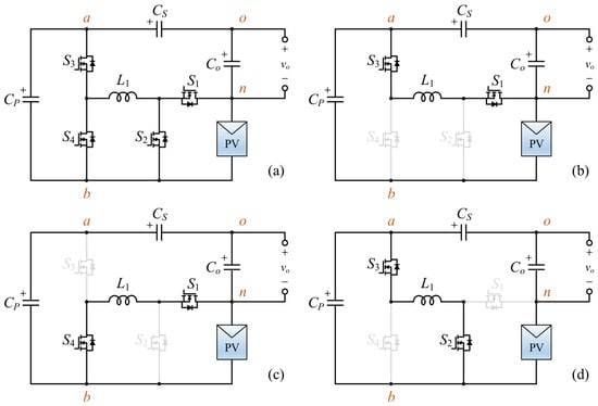
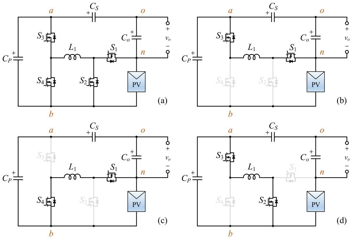
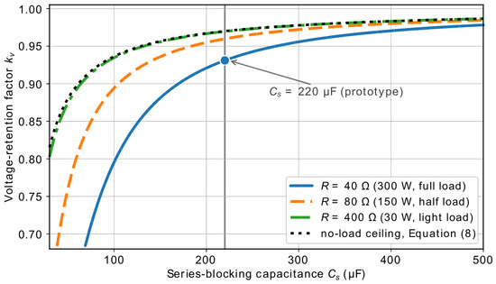
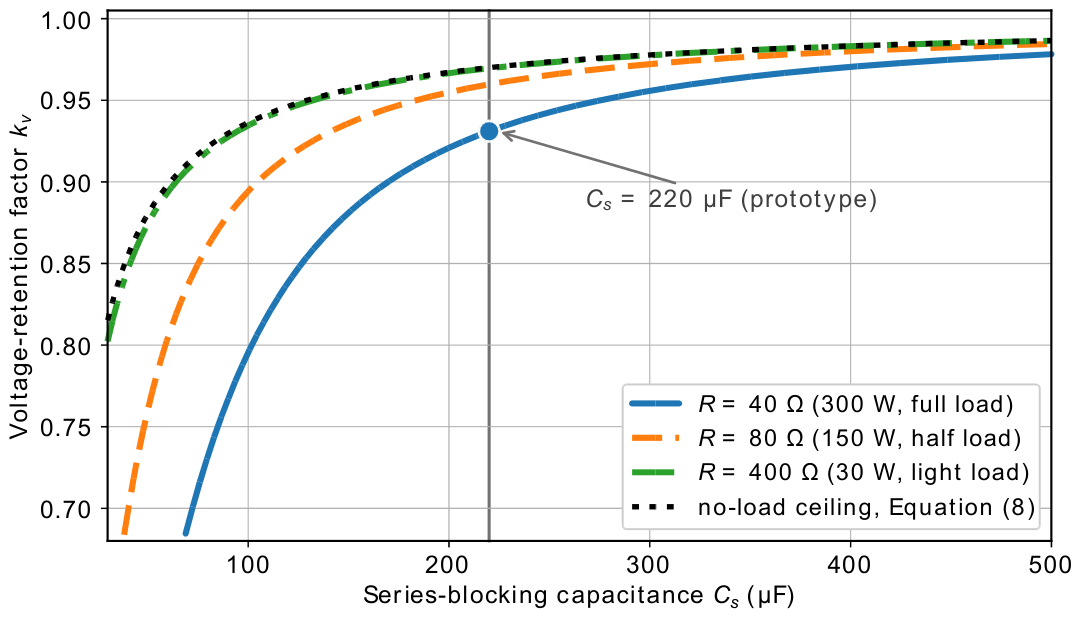
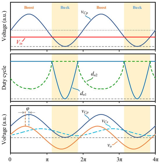
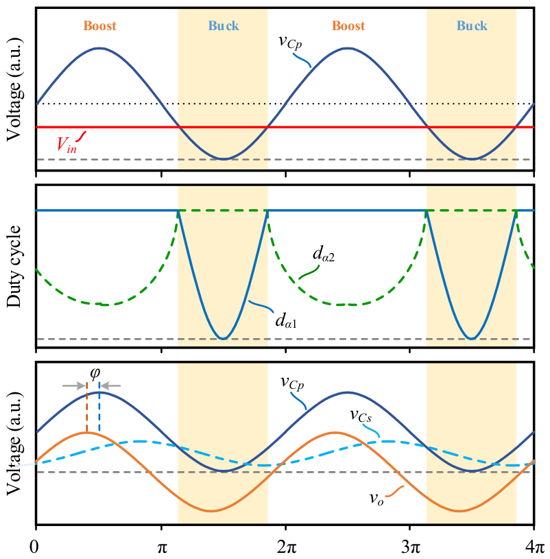
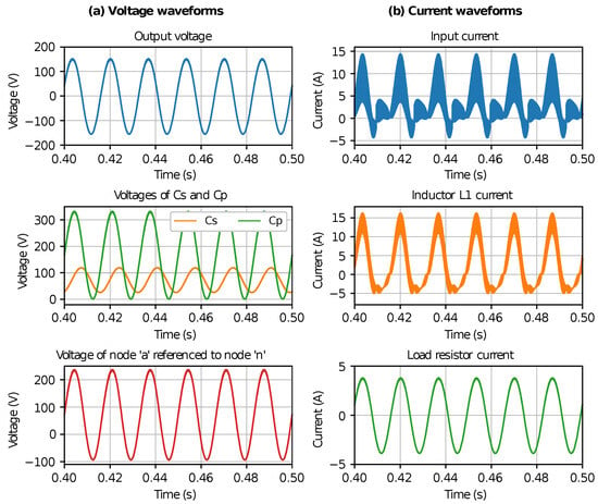
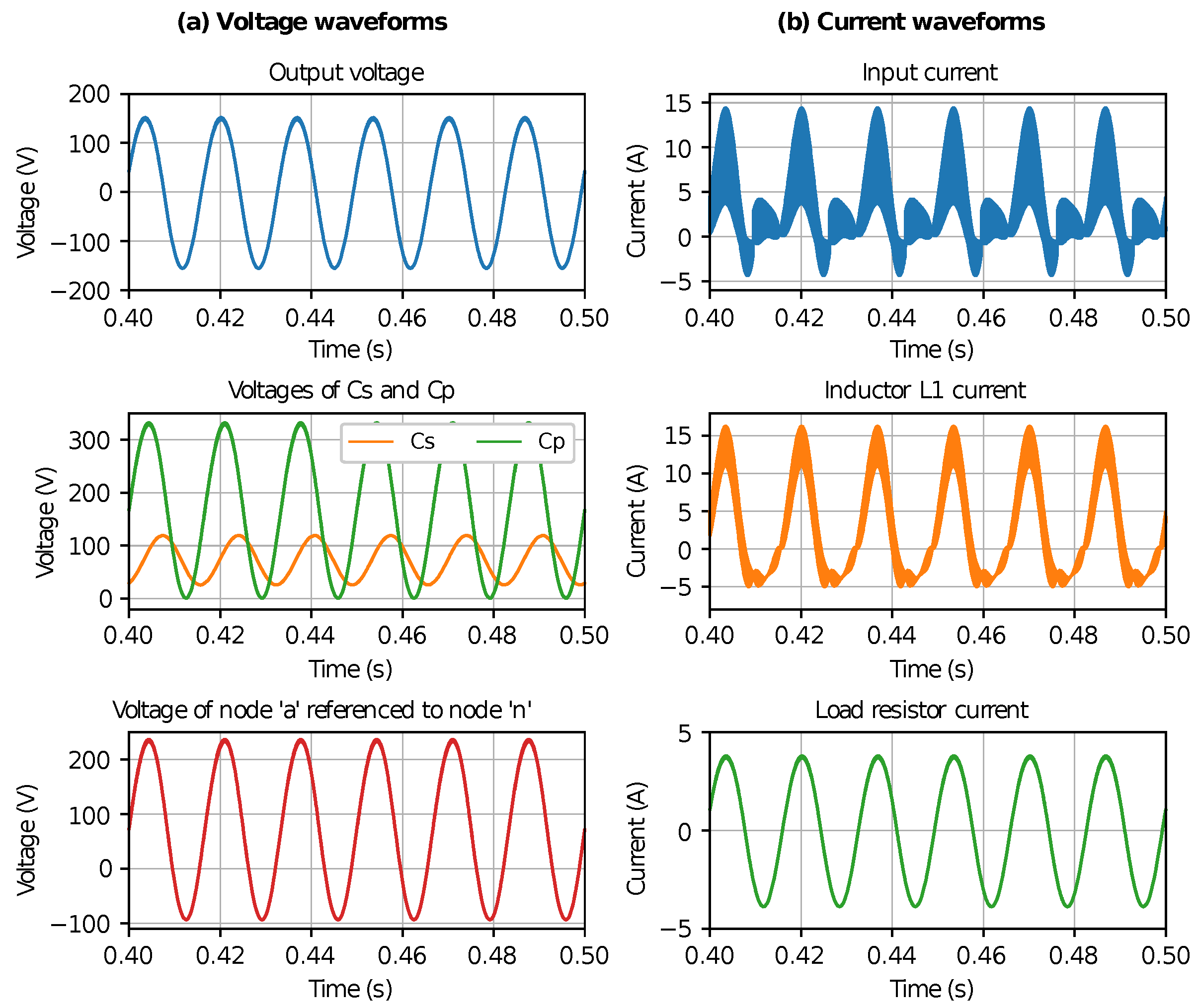
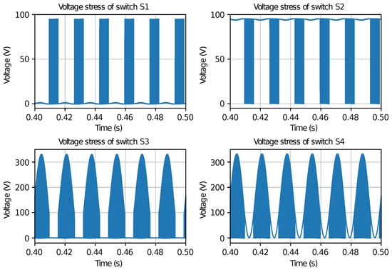
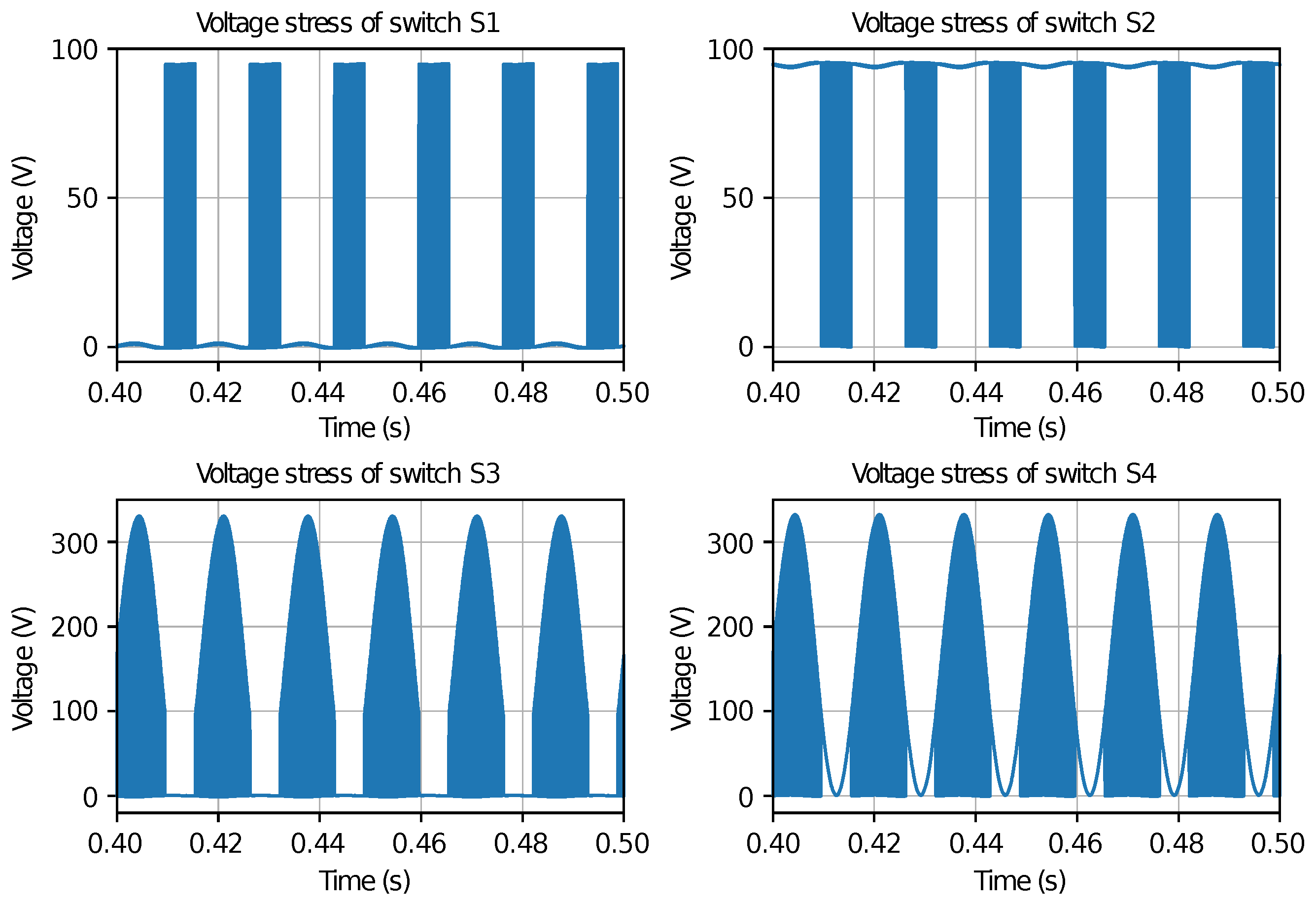
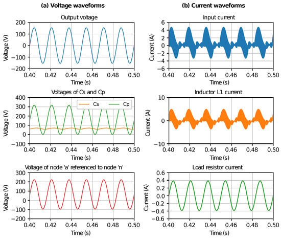
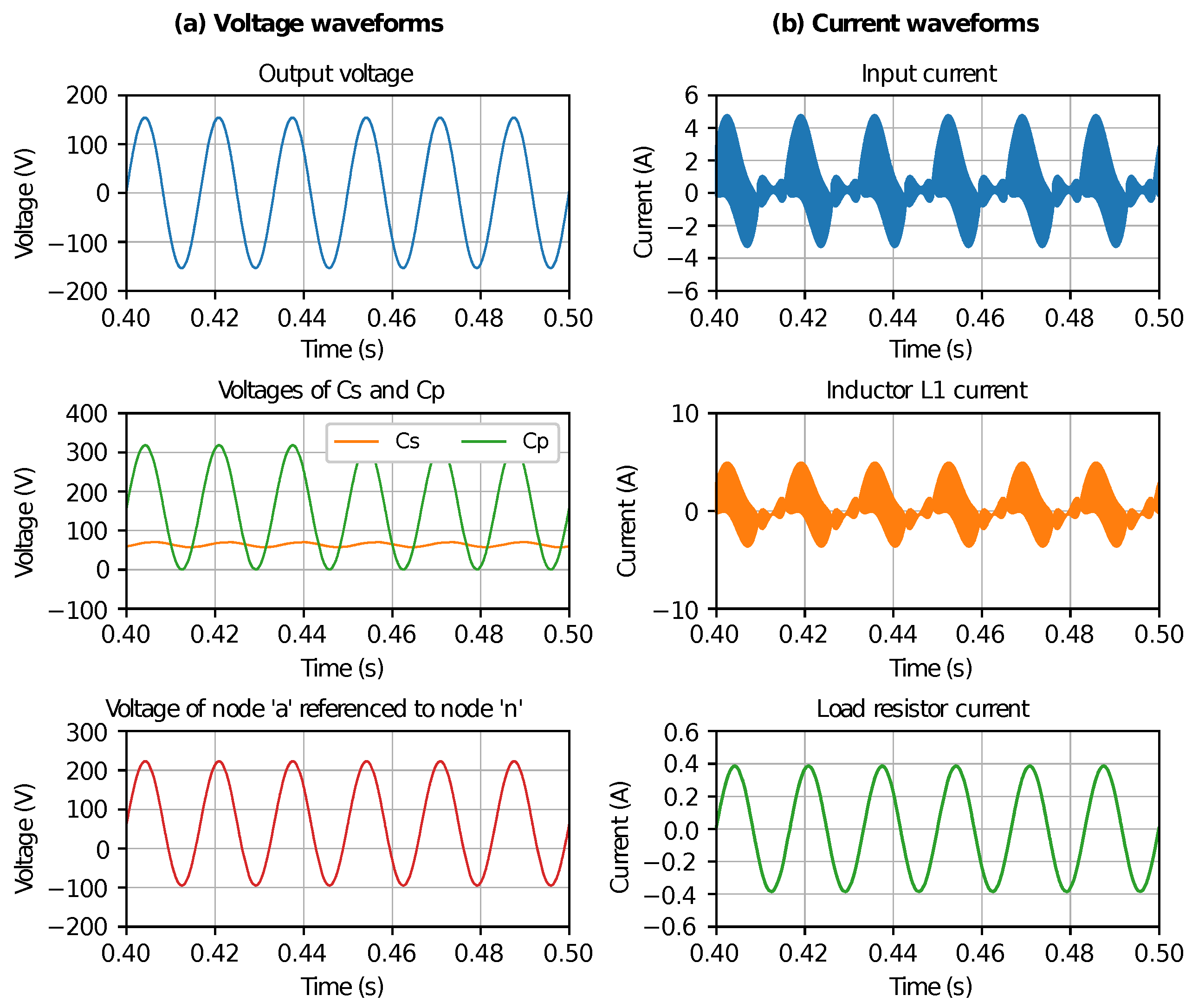
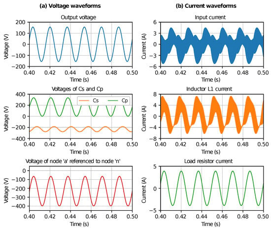
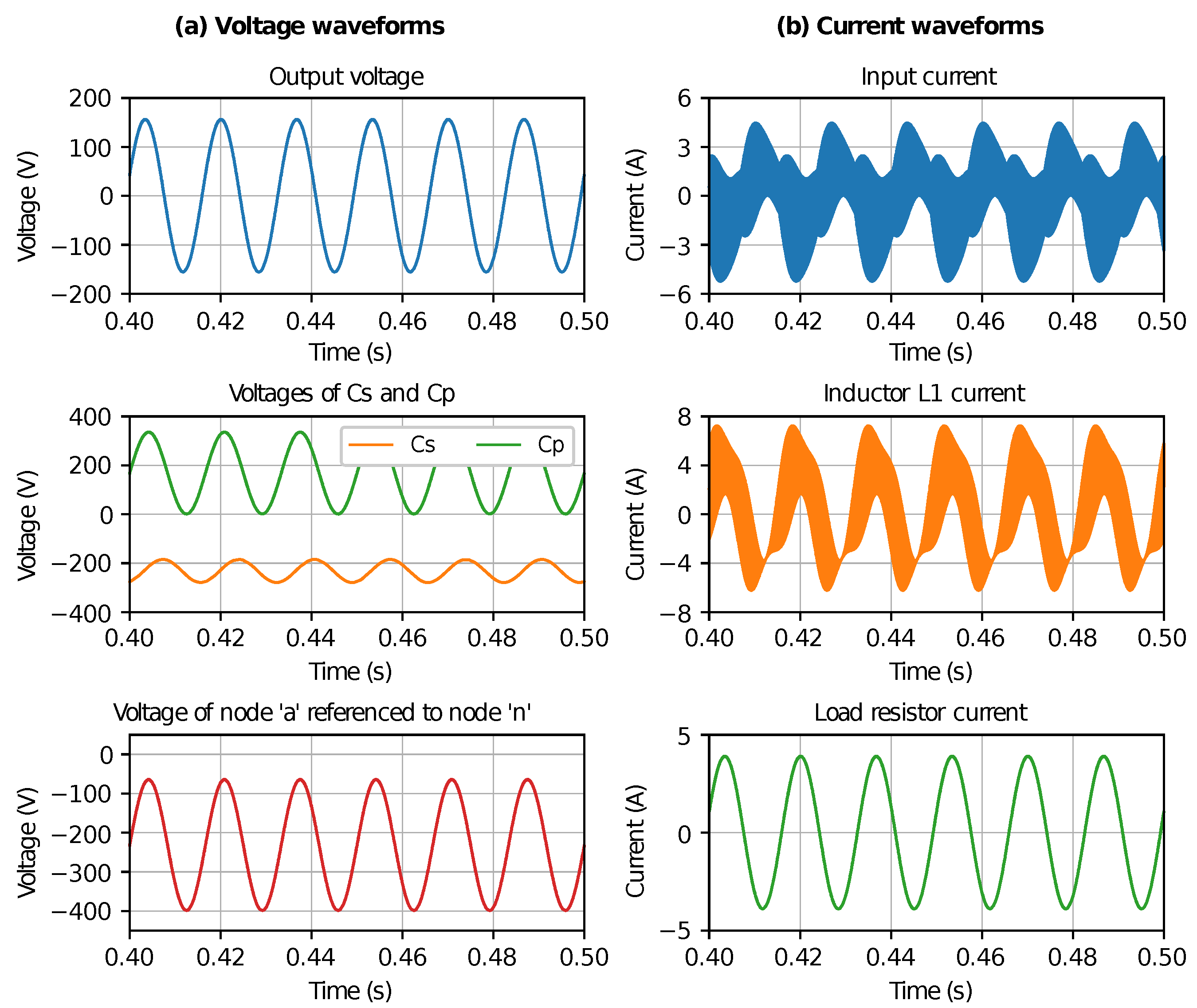
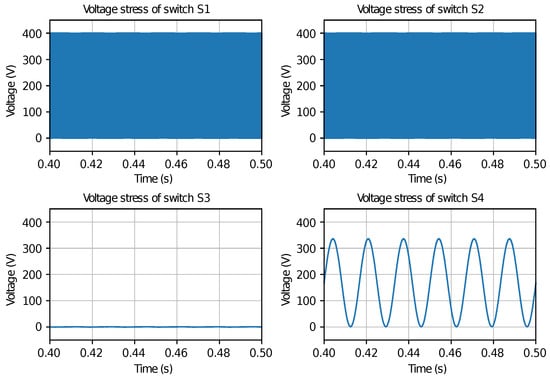
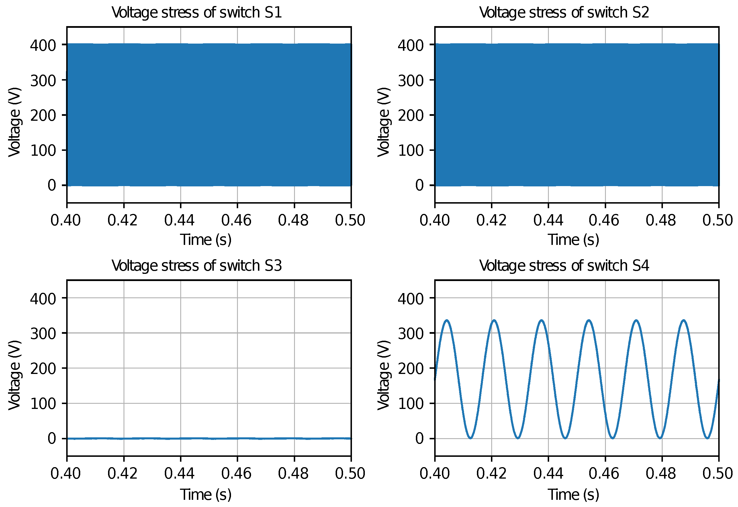
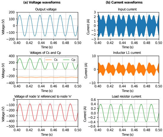
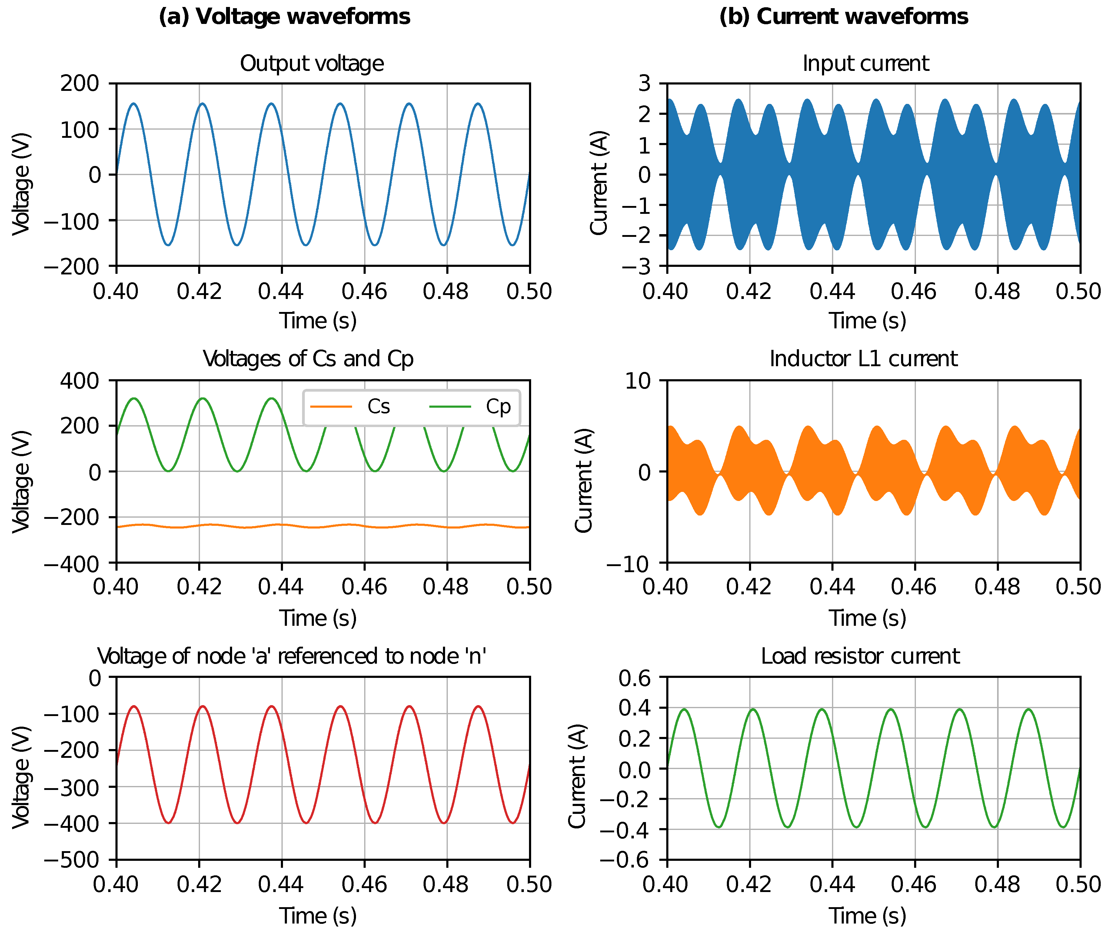
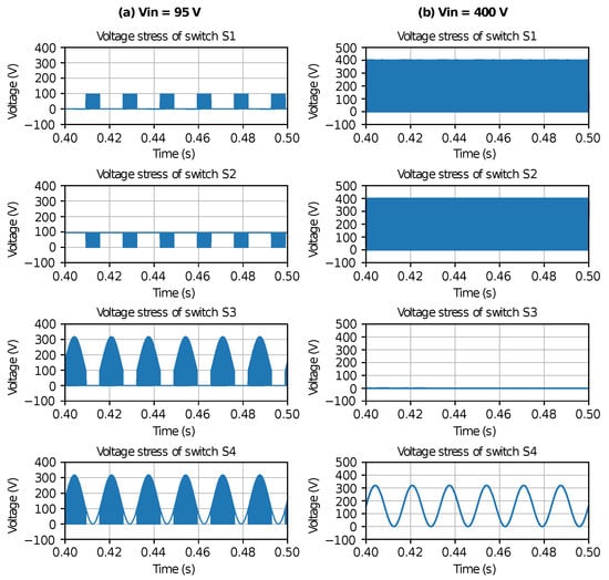
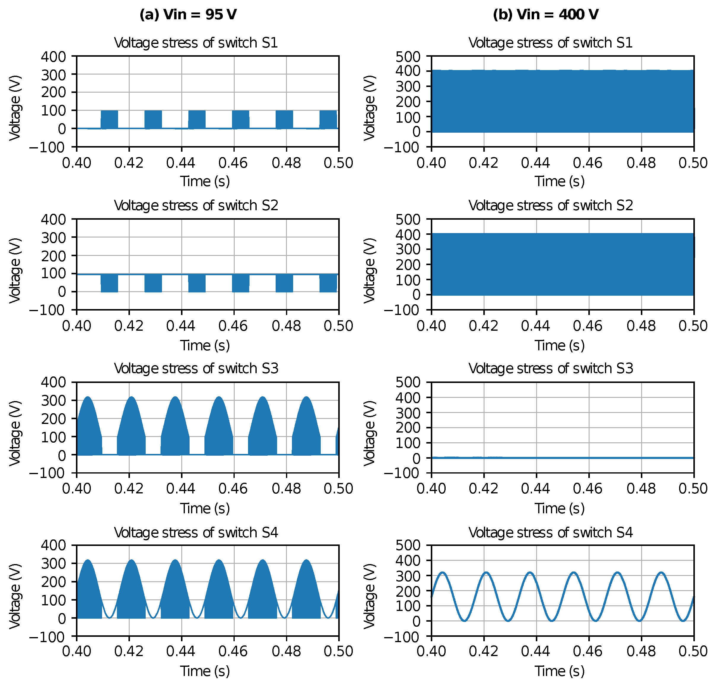
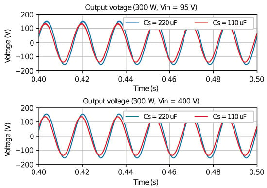
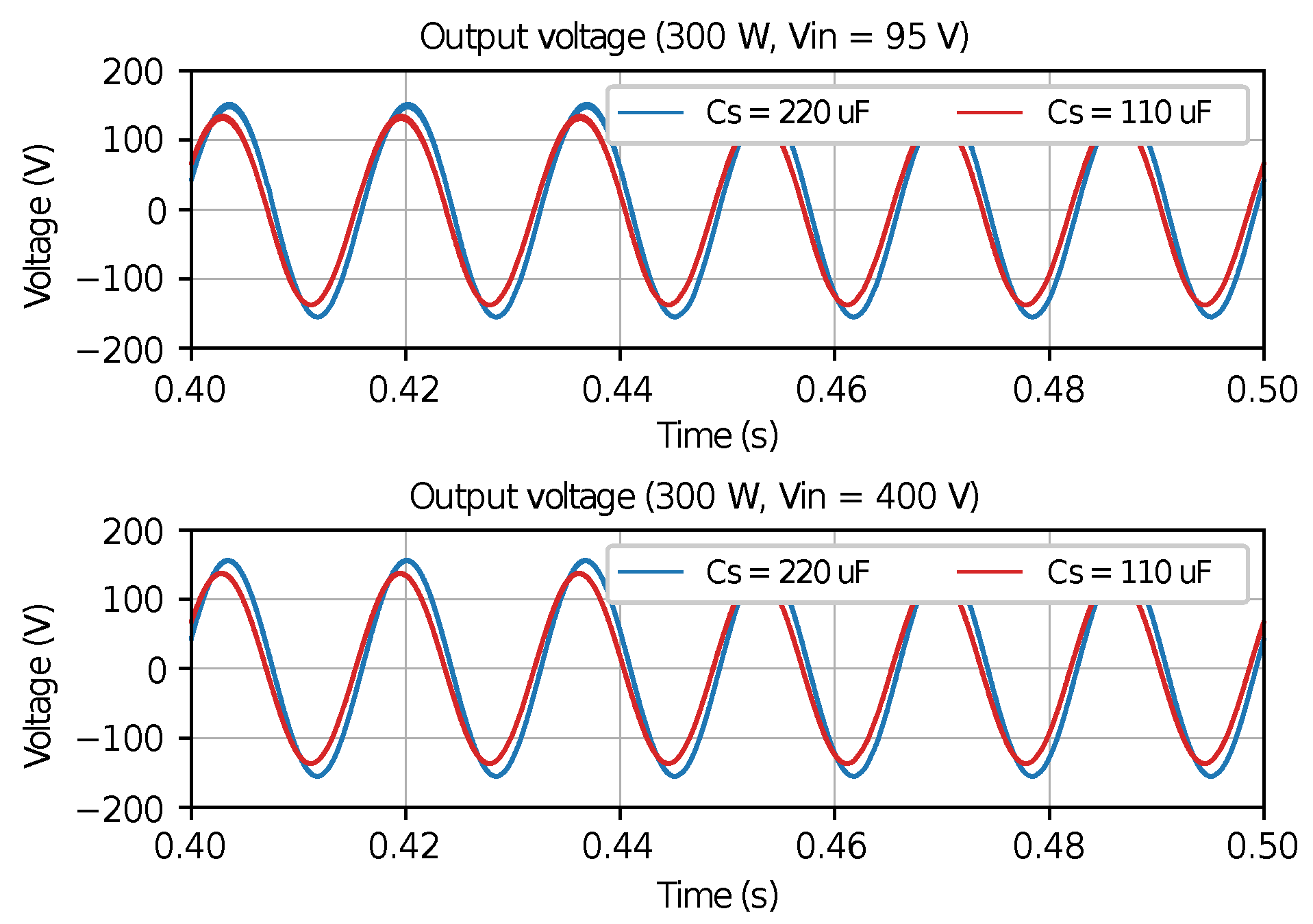
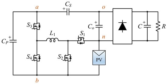
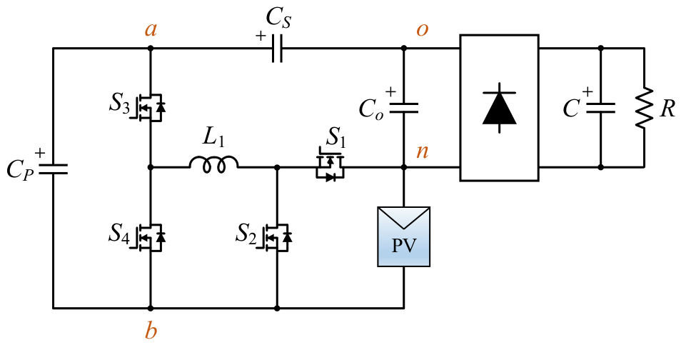
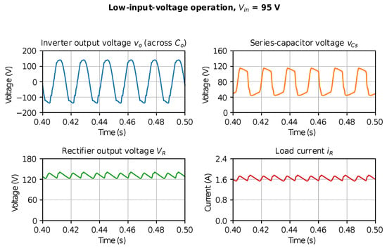
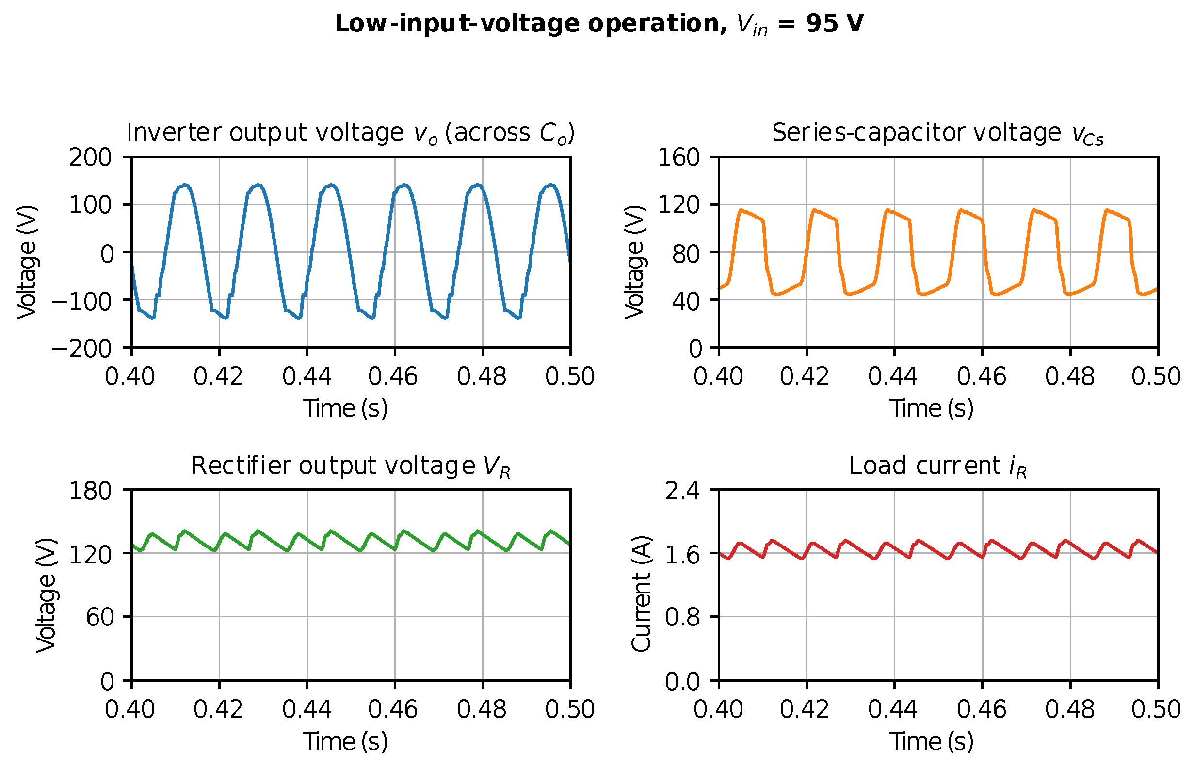
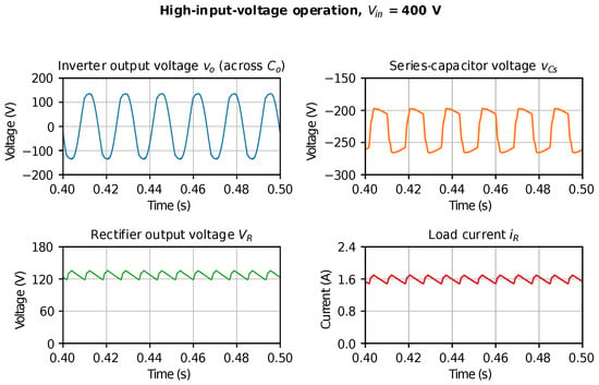
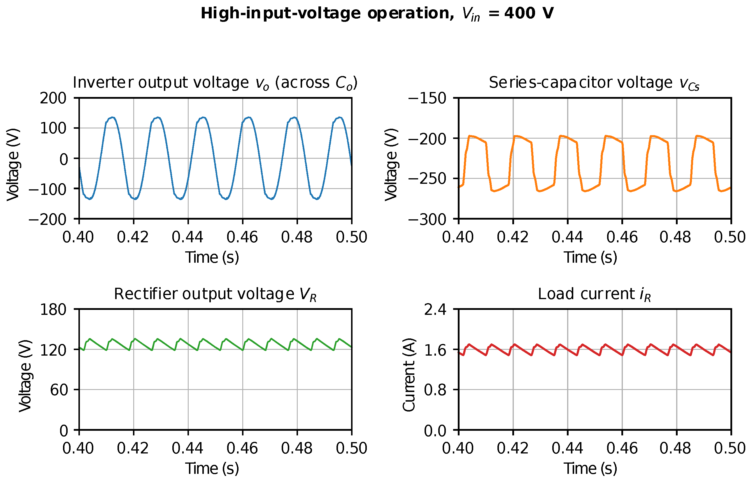
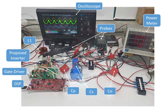
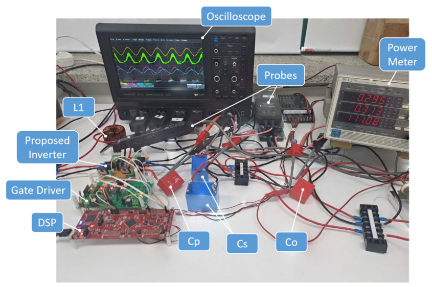
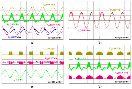
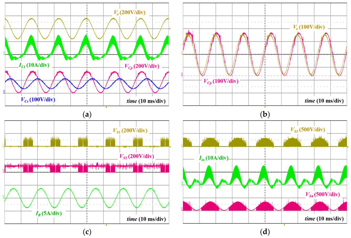
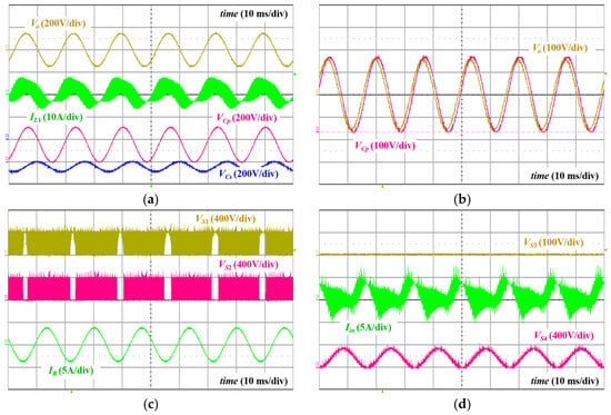
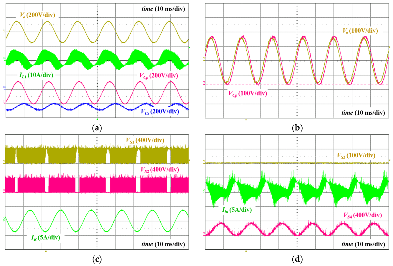
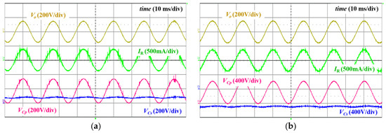
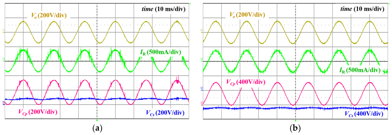
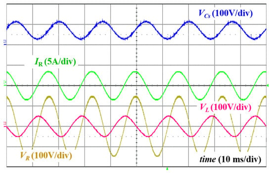
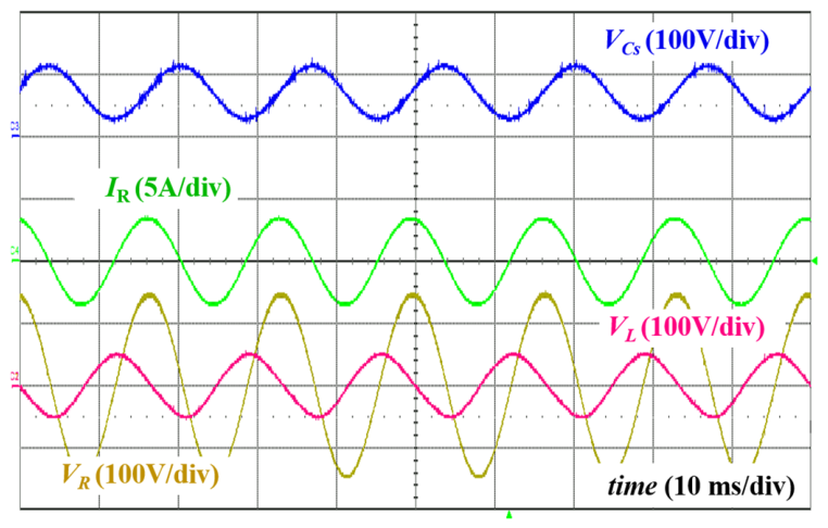
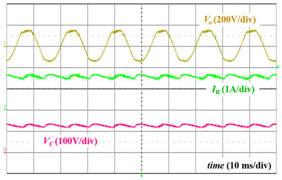
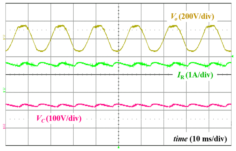
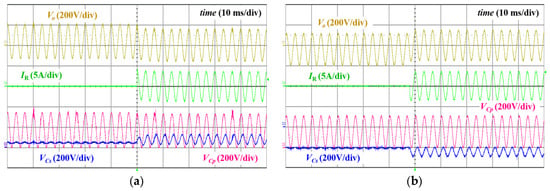
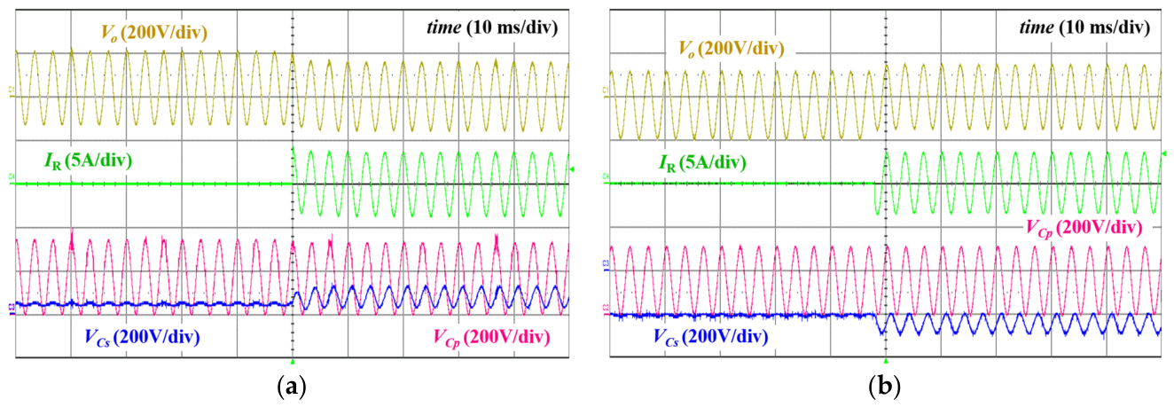
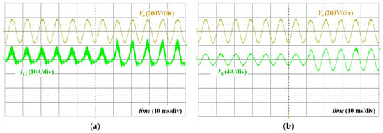
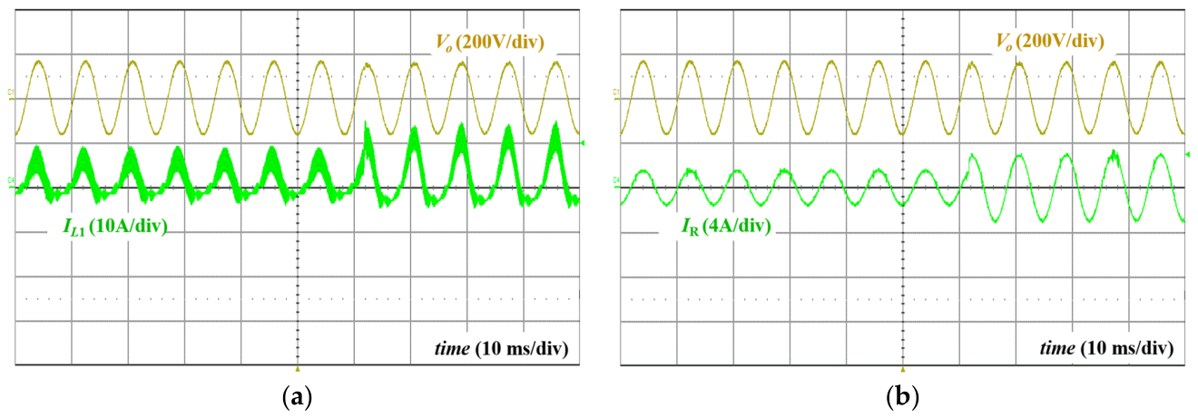
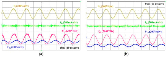
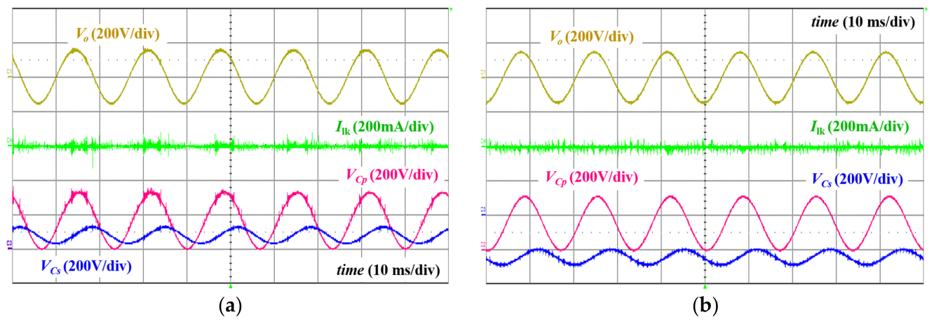
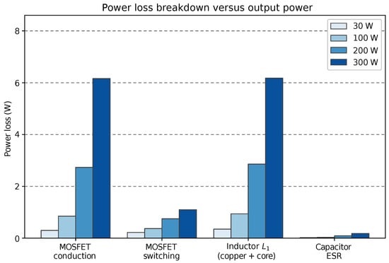
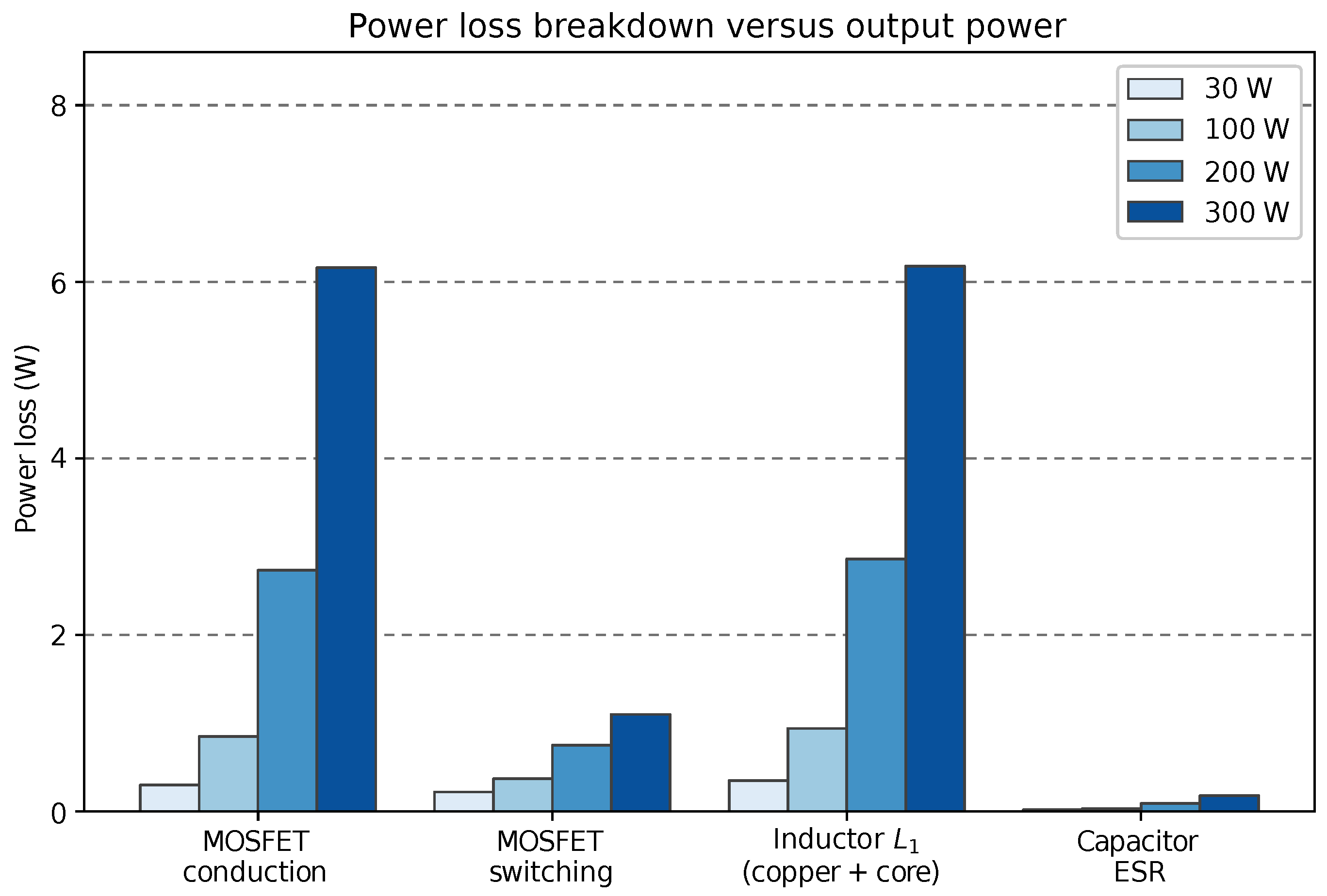
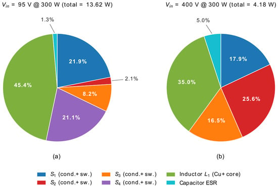
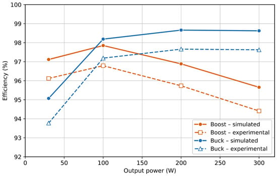

Disclaimer/Publisher’s Note: The statements, opinions and data contained in all publications are solely those of the individual author(s) and contributor(s) and not of MDPI and/or the editor(s). MDPI and/or the editor(s) disclaim responsibility for any injury to people or property resulting from any ideas, methods, instructions or products referred to in the content. |
© 2026 by the authors. Licensee MDPI, Basel, Switzerland. This article is an open access article distributed under the terms and conditions of the Creative Commons Attribution (CC BY) license.