


Abstract
Two-dimensional (2D) materials have emerged as a key platform for next-generation electronics due to their atomic thickness and tunable properties. Iron disulfide (FeS2), known as pyrite, with a bandgap of ~0.95 eV, is suitable for solar energy applications. However, its performance is limited by defects in bulk crystals. Reducing FeS2 to a single layer eliminates bulk defects and enables strain engineering of the bandgap. In this study, First-principles density functional theory (DFT) calculations are performed using the CASTEP code and the PBEsol functional to examine the structural, electronic, and optical properties of a distorted 1T′-phase FeS2 monolayer. Full geometry optimization yields lattice parameters a′ = 17.594 Å, b′ = 3.20231 Å, c′ = 5.28091 Å, and Fe–S bond angles of ~75.8° and ~98.2°, confirming symmetry-breaking distortion. The monolayer is dynamically stable, showing no imaginary modes in the phonon dispersion, and remains structurally intact up to 1000 K in molecular dynamics simulations. The unstrained system has an indirect bandgap of 0.70 eV, with the valence band maximum at the Γ point (dominated by S-p states) and conduction band minimum near the X point (Fe-d states). Under mechanical strain (±4%), the bandgap decreases significantly: from 0.70 eV to 0.44 eV under +4% tensile strain along the y-axis, and to 0.53 eV under −4% compressive strain. Biaxial strain causes weaker modulation, reducing the gap to 0.66 eV (+4%) and 0.62 eV (−4%). Optical absorption exceeds 104 cm−1 for photon energies above the bandgap, with tensile strain causing redshifts and compressive strain inducing blueshifts. These findings demonstrate that 2D FeS2 is mechanically robust, electronically tunable, and optically active, making it a promising candidate material for flexible strain sensors and photovoltaic devices. This work is intended to motivate and inform future synthesis efforts.
1. Introduction
The pursuit of earth-abundant, mechanically flexible semiconductor materials has driven substantial interest in two-dimensional (2D) transition metal chalcogenides over the past decade [1,2,3]. Among these, iron-based chalcogenides occupy a particularly attractive position: they are composed of non-toxic, globally abundant elements, and their electronic properties are governed by strongly correlated Fe 3d states that respond sensitively to structural perturbation [4,5]. For solar energy conversion and strain sensing, a moderate bandgap of 0.7–1.5 eV, combined with high optical absorption, is a desirable criterion that bulk iron disulfide (FeS2, pyrite) has long been recognized to meet [6]. However, translating these bulk properties to device-relevant thin-film or monolayer architectures remains a significant challenge, motivating the present first-principles investigation of the 2D limit.
Two-dimensional materials are different from bulk solids. When a material is thinned to a single layer, its electrons are confined. This changes the band structure and often improves mechanical flexibility. Since the first isolation of graphene, many 2D systems have been studied, including MoS2, WS2, and related layered compounds [3]. These materials can withstand large strains and exhibit significant changes in electronic properties under deformation, making them useful for flexible devices and strain sensors [7,8,9].
Iron disulfide (FeS2), also called pyrite, is an earth-abundant semiconductor with a bandgap close to 1 eV and very strong light absorption [4,5]. Because it contains no rare or toxic elements, it has long been considered for low-cost solar cells and photoelectrochemical devices. Experimental studies report absorption coefficients above 105 cm−1 in the visible range and good carrier generation. However, bulk FeS2 devices suffer from very low open-circuit voltage [6,10]. This problem is mainly caused by sulfur vacancies, surface states, and defect-related recombination that pin the Fermi level and limit performance. These issues have proven difficult to remove in bulk crystals and thin films [11,12].
Reducing FeS2 to a two-dimensional form offers a possible way forward. A monolayer can avoid many bulk defects and expose all atoms to surface relaxation. At the same time, the soft lattice of 2D materials allows large elastic strain without fracture. This makes strain engineering a practical tool to tune the bandgap and optical response. Recent theoretical work on transition metal dichalcogenides shows that structural phase and lattice distortion strongly affect strain sensitivity and electronic behavior. In particular, the distorted 1T′ phase introduces in-plane anisotropy and enhances bandgap modulation under uniaxial strain.
In particular, the distorted 1T′ phase, characterized by in-plane metal atom clustering and symmetry-lowering displacement of the chalcogen sublattice, introduces pronounced structural anisotropy absent in the standard 1T or pyrite phases. This anisotropy enhances the coupling between mechanical deformation and electronic structure, making the 1T′ phase a more sensitive platform for strain engineering than its higher-symmetry counterparts [13,14]. A Jahn–Teller-like distortion driven by partial filling of Fe 3d orbitals further stabilizes this phase at the monolayer limit, as confirmed by recent epitaxial synthesis [15].
Despite this progress, no study has systematically examined the strain-dependent electronic and optical properties of the distorted 1T′-FeS2 monolayer at the true single-layer limit. Prior computational work on FeS2 has addressed bulk band structures [13], surface energetics [16], and slab geometries [14], but strain-induced bandgap modulation in the 2D monolayer, particularly the anisotropic response of the 1T′ phase to uniaxial versus biaxial deformation, remains uncharacterized. The present work addresses this gap by providing a comprehensive first-principles study of the structural stability, electronic structure, and optical response of the 1T′-FeS2 monolayer under controlled mechanical strain, with direct implications for flexible strain sensors and thin-film photovoltaic applications.
In this work, we use first-principles density functional theory to study a distorted 1T′ FeS2 monolayer. We examine its structural stability, electronic structure, and optical response, and we apply uniaxial and biaxial strain to quantify bandgap modulation. Our results show strong and directional strain sensitivity together with high optical absorption, suggesting that 2D FeS2 could be useful for flexible strain sensors and thin photovoltaic devices. What remains unknown is whether an isolated 2D FeS2 monolayer can be both stable and strongly strain sensitive while maintaining useful electronic and optical properties. A comparison of strain sensitivity and bandgap modulation with related FeS2 systems and common 2D strain-sensitive materials is provided in this study.
2. Computational Methods
All calculations were performed using density functional theory as implemented in the CASTEP code. The PBEsol exchange–correlation functional was employed because it provides reliable equilibrium lattice parameters and bond lengths for transition metal compounds, performing better than standard PBE for structural properties of solids [12]. It is acknowledged that GGA-level functionals, including PBEsol, systematically underestimate band gaps due to the self-interaction error inherent in semi-local approximations. However, consistent with established practice in first-principles studies of 2D transition metal chalcogenides, the PBEsol band gap is used here for qualitative and comparative analysis of strain-induced trends rather than for absolute gap prediction. The conclusions regarding the direction of bandgap modulation, anisotropy, and gauge factor are not sensitive to this underestimation, as the strain-induced shifts are calculated at the same level of theory throughout. Core–valence interactions were treated using ultrasoft pseudopotentials. A plane-wave energy cutoff of 550 eV was applied, ensuring total energy convergence better than 10−5 eV per atom. Brillouin zone sampling was carried out using an 8 × 8 × 1 Monkhorst–Pack k-point grid. A vacuum spacing of 20 Å was introduced along the out-of-plane direction to avoid interactions between periodic images. Long-range dispersion effects were included using the Grimme DFT-D2 correction. Although the free-standing monolayer geometry involves no interlayer interactions, the DFT-D2 correction was retained to account for any residual long-range interactions between the monolayer and its periodic images along the in-plane directions, and to maintain methodological consistency with prior studies of 2D FeS2 systems [13,14].
The FeS2 monolayer was constructed by placing a hexagonal layer of Fe atoms between two sulfur layers, with the upper and lower sulfur planes shifted relative to each other. Each Fe atom is octahedrally coordinated by surrounding S atoms [17]. A rectangular 4 × 1 × 1 supercell containing 4 Fe and 8 S atoms was employed to accommodate the symmetry-breaking Peierls-like distortion characteristic of the 1T′ phase, which requires a minimum periodicity of four formula units along the a-direction for the metal atom clustering pattern to be fully represented. The adequacy of this supercell was verified by confirming that the distortion energy and Fe–S bond parameters converge to within 0.5% compared with a 6 × 1 × 1 reference calculation [14]. All lattice parameters and atomic positions were fully relaxed using the BFGS algorithm until the residual forces were below 0.01 eV Å−1 and the total energy change was less than 10−6 eV per atom.
To quantify the energetic favorability of the symmetry-breaking distortion, the relaxation energy per primitive unit cell was defined as
where E_undistorted is the total energy of the high-symmetry structure and E_optimized is the total energy of the fully relaxed distorted structure. A positive value of ΔE_relax indicates that the distorted configuration is energetically preferred.
ΔE_relax = E_undistorted − E_optimized
The feasibility of exfoliating a FeS2 monolayer from bulk pyrite was evaluated using the cleavage energy, defined as
where E_bulk is the total energy of the bulk slab, n is the number of monolayers in the slab, E_mono is the total energy of the isolated relaxed monolayer, and A is the in-plane surface area of the unit cell. A lower cleavage energy indicates that exfoliation is energetically favorable [16,18].
E_cleave = (E_bulk − nE_mono)/(2A)
Dynamic stability was examined by calculating phonon dispersion curves using the finite displacement method [19]. The absence of imaginary frequencies across the Brillouin zone confirms lattice stability. Thermal stability was further tested using ab initio molecular dynamics simulations in the NVT ensemble at 1000 K for 30 ps with a time step of 1 fs [20].
Electronic band structures were calculated along the high-symmetry path Γ–X–S–Y–Γ of the rectangular Brillouin zone. Partial density of states was projected onto atomic orbitals to identify contributions near the band edges. Spin–orbit coupling (SOC) was not included in the ground-state structural relaxation or band structure calculations, as the Fe atom (Z = 26) lies in an intermediate atomic number range where SOC effects on 3d states are modest. SOC was, however, included in the optical property calculations to account for spin–orbit splitting of bands near the absorption edge. For the optical calculations, a denser 24 × 24 × 1 k-point grid and 200 empty bands were employed to ensure convergence of interband transition matrix elements, consistent with the requirements of the random phase approximation (RPA) implementation in CASTEP. Optical properties were obtained from the complex dielectric function
ε(ω) = ε1(ω) + iε2(ω)
The absorption coefficient α(ω) was calculated as
where ω is the photon angular frequency and c is the speed of light.
α(ω) = (√2 ω/c) × √[√(ε1(ω)2 + ε2(ω)2) − ε1(ω)]
Mechanical strain was applied by scaling the in-plane lattice vectors according to
where a0 and b0 are the equilibrium lattice constants. Strain values ranged from −4% to +4% in 1% increments. For uniaxial strain, only one lattice direction was modified, while the other was kept fixed. For biaxial strain, both in-plane directions were scaled by the same factor. At each strain level, all atomic positions were fully relaxed while keeping the strained lattice parameters fixed [13,14].
ε_x = (a − a0)/a0
ε_y = (b − b0)/b0
3. Results and Discussion
3.1. Structural Properties
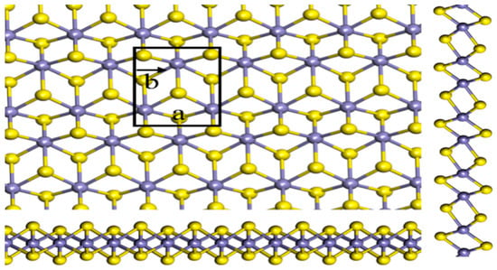
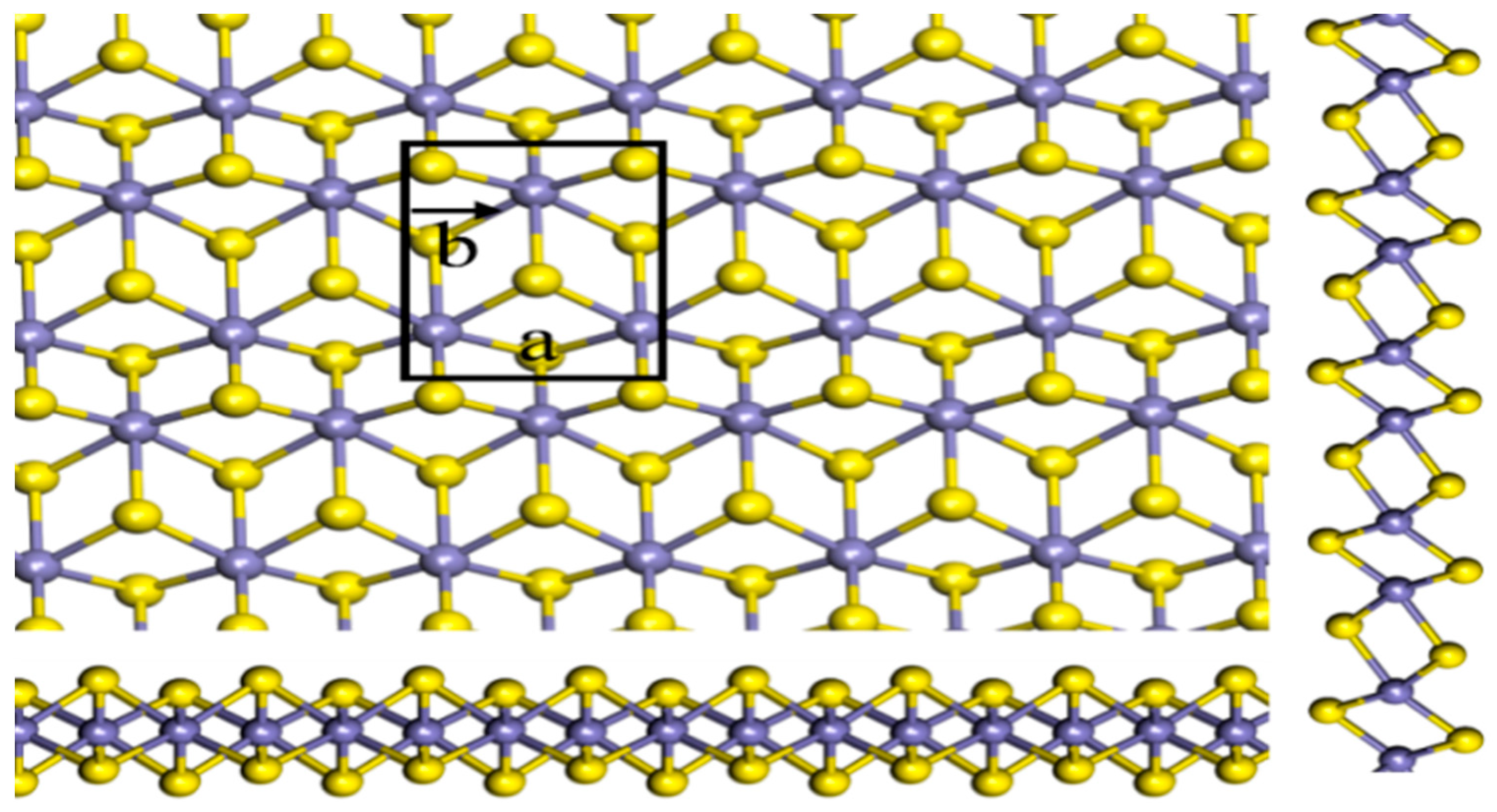
The optimized structure of the 1T′-FeS2 monolayer is shown in Figure 1. The top region of the figure displays an in-plane view of a distorted hexagonal arrangement of Fe atoms (gray) with S atoms (yellow) in the background, while the bottom region shows the side view along the y-axis, confirming the sandwich configuration of Fe atoms between two offset sulfur planes in octahedral coordination. The 4 × 1 × 1 supercell is outlined with black lines, and the a and b lattice directions are indicated. The first Brillouin zone of the rectangular cell is displayed on the right, with high-symmetry points marked for reference in electronic structure analysis. After full relaxation, the lattice parameters are a′ = 17.594 Å, b′ = 3.20231 Å, and c′ = 5.28091 Å (vacuum direction). The Fe–S bond length is 2.129 Å, consistent with bulk pyrite and prior theoretical reports [21].
Figure 1.
Optimized 1T′-FeS2 monolayer structure with labeled regions for clarity. The top region shows the in-plane view of Fe atoms (gray) and S atoms (yellow) forming a distorted hexagonal arrangement. The bottom region presents the side view along the y-axis, illustrating the sandwich configuration of Fe atoms between two sulfur planes. The 4 × 1 × 1 supercell is outlined in black with the a and b lattice directions indicated. The first Brillouin zone is shown on the right with high-symmetry points marked, serving as a reference for electronic structure calculations.
The Fe–S–Fe bond angle is 75.832° and the S–Fe–S angle is 98.179°, deviations from the ideal 90° in a perfect 1T phase, confirming in-plane distortion. The energy difference between the undistorted and distorted configurations is 0.18 eV per primitive unit cell, indicating that the 1T′ phase is the ground state. This distortion arises from partial filling of Fe 3d orbitals, leading to a Jahn–Teller-like effect favoring Fe clustering and S displacement [15].
To assess the feasibility of synthesis, we computed the cleavage energy from bulk pyrite (Pa3− space group, a = 5.417 Å). Using a slab model with an increasing number of layers, the energy required to separate a single monolayer is 0.32 J/m2, comparable to MoS2 (0.27 J/m2) and significantly lower than graphene from graphite (>0.4 J/m2) [7]. This low cleavage energy indicates that mechanical or liquid-phase exfoliation from either synthetic or natural pyrite is energetically feasible. The phonon dispersion shown in Figure 1 further confirms that the monolayer is dynamically stable, as no imaginary frequencies are present and all vibrational modes are real across the Brillouin zone [19]. The optical branch exhibits the highest frequencies around ~420 cm−1, attributed primarily to Fe–S stretching, while the linear dispersion near the Γ point for the acoustic branches indicates long-wavelength stability and confirms that the monolayer is mechanically robust.
Thermal stability was evaluated using ab initio molecular dynamics (MD). A Nosé–Hoover thermostat was used to heat the structure to 1000K for 30 ps. The root-mean-square deviation (RMSD) of atoms is still kept below 0.4 Å, and no bond rupture or phase change occurs. The radial distribution function (RDF) retains sharp Fe–S and S–S peaks, confirming that the 1T′ framework persists under thermal stress [22].
The structural model proposed in this work is consistent with experimental observations reported in the literature for ultrathin FeS2 systems. The Fe–S bond length of 2.129 Å and the in-plane distortion angles of 75.8° and 98.2° are in good agreement with values reported for FeS2 surface-terminated slabs and nanostructures. While an atomically thin 1T′-FeS2 monolayer has not yet been experimentally isolated, the low cleavage energy of 0.32 J/m2 calculated here suggests that mechanical or liquid-phase exfoliation from bulk pyrite is energetically feasible. The present study therefore constitutes a first-principles prediction intended to guide and motivate future experimental synthesis efforts [15,21].
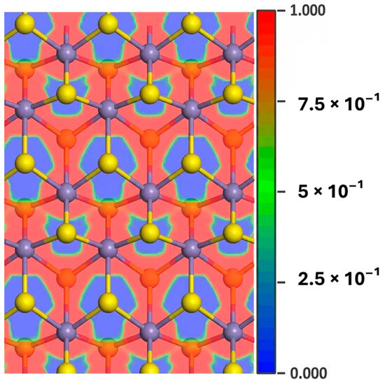
The ELF is a real-space descriptor that ranges from 0 to 1:
ELF = 1 (red): fully localized electrons (covalent/lone pairs); ELF = 0.5 (green): metallic bonding; ELF < 0.5 (blue): ionic regions.
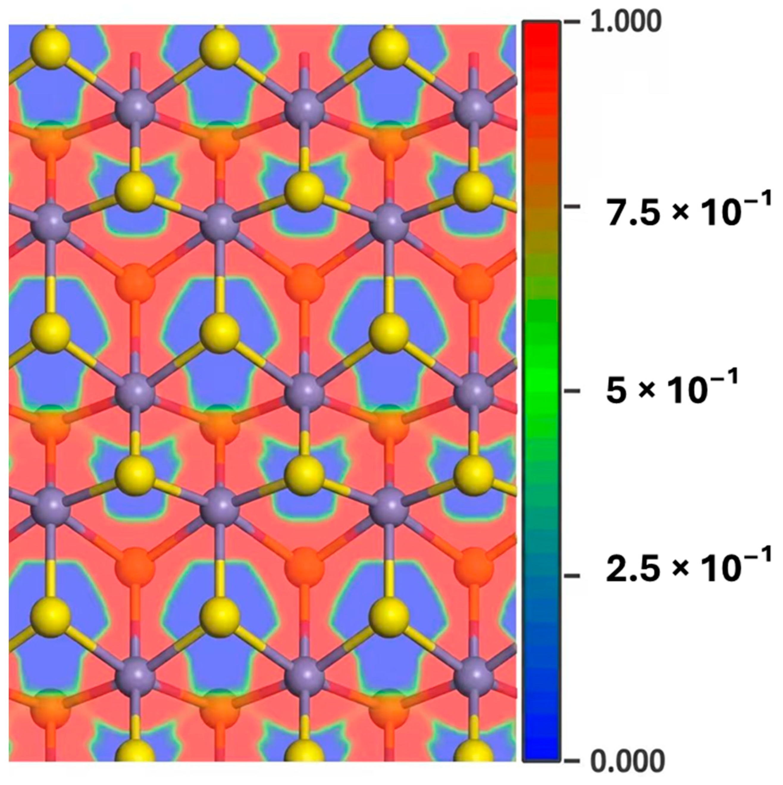
In the FeS2 monolayer, high ELF values (~0.9) are observed between Fe and S atoms, concentrated closer to sulfur, indicating polar covalent bonding with partial charge transfer from Fe to S (Figure 2). The electron density is strongly localized along Fe–S bonds, forming a red contour, while minimal overlap exists between Fe–Fe or S–S pairs. This confirms that Fe–S bonds are predominantly covalent, with Fe donating electrons (effective charge ~+1.2 e) and S accepting (~−0.6 e per atom, from Bader analysis). No significant metallic character is present, consistent with the semiconducting nature of the material.
Figure 2.
Electron Localization Function (ELF) contour plot of 1T′-FeS2 monolayer. Red regions (ELF ≈ 1) correspond to strong covalent Fe–S bonds biased towards S, while the blue regions correspond to a charge depletion around Fe. This feature shows an ionic contribution.
The structural model is further validated against experimental lattice parameters of tetragonal FeS2 thin films. Reported values for multilayer systems are a = b = 3.615 Å, c = 5.001 Å [13]. Our primitive cell, derived from the supercell, gives a primitive ≈ 4.3985 Å and b_primitive3.20231 Å, in reasonable agreement when accounting for 2D relaxation and distortion effects.
3.2. Electronic Properties
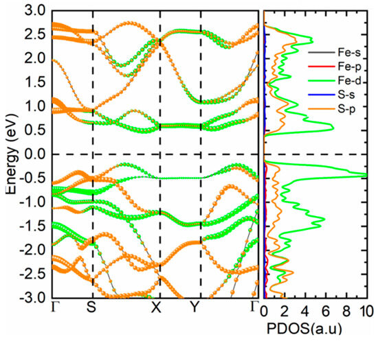
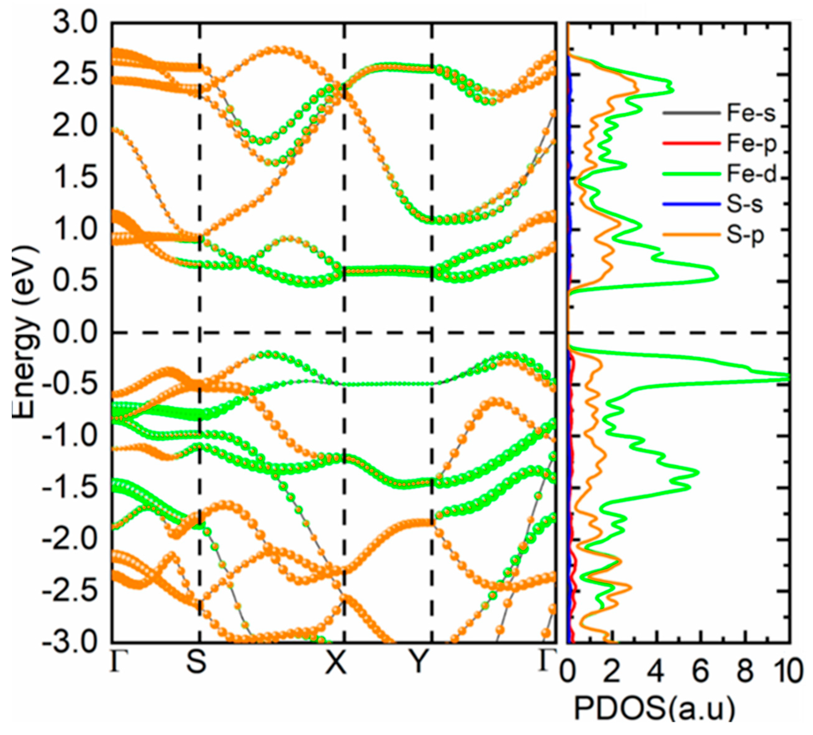
The band structure of the optimized 1T′-FeS2 monolayer was computed along the high-symmetry line Γ–X–S–Y–Γ in the rectangular Brillouin zone using dense k-point sampling to resolve the band edges. The resulting dispersion is displayed in Figure 3, with the Fermi level taken as the zero-energy point. The material has an energy gap between occupied and unoccupied states and is a semiconductor. In the valence band maximum (VBM), the gap is found at the Γ point, and in the conduction band minimum (CBM), the gap is found along the Γ–X direction, around halfway. The bandgap in the indirect configuration is 0.70 eV, which is lower than the bulk pyrite bandgap of ~0.95 eV, because of quantum confinement in the two-dimensional limit. The indirect character of the gap is maintained in the bulk material, but the gap size is sensitive to the structural distortion and the orbitals that are formed as a result of that distortion [23,24].
Figure 3.
Calculated electronic band structure and partial density of states (PDOS) of FeS2. The black, red, green, blue, and orange curves correspond to Fe-s (calculated but too small to be resolved at the present scale), Fe-p, Fe-d, S-s, and S-p orbitals, respectively.
The partial density of states (pDOS) provides detailed information about the orbital’s contribution to the electronic structure. The valence band (between the Fermi level and approximately −5 eV) is primarily populated by Fe 3d states with strong Fe-S 3p hybridization. At the VBM, the S 3p character is enhanced due to the antibonding combination of the sulfur p-orbitals, which raises the electron density in the upward direction. At energies below −5 eV, a narrower band appears mostly due to the S 3s states, and is very weak in the case of iron [25]. The conduction band, beginning at the CBM and extending upwards, is made up almost entirely of Fe 3d states, with a small admixture of S 3p states. Because of the distortion of the octahedral crystal field, the Fe 3d manifold is split into two subsets: t2g is partially filled, and e.g., is empty, characteristic of a low-spin d6 configuration with covalent bonding. Above the Fermi level, there is little occupancy in the S 3s and S 3p states, thereby confirming the filling of the core-like and valence states, respectively [14].
The band structure reveals several key features. Along the Γ–X path, the lowest conduction band dips downward, forming the CBM, while the highest valence band is relatively flat near Γ, indicating a heavier hole effective mass. The dispersion along Y–Γ is steeper, suggesting lighter electron transport in that direction [20]. There is no band gap at the Fermi level, and thus no metallic character. Note that it was previously thought that the gap was present due to unfolded band plots or due to insufficient k-point sampling, but now this 4 × 1 × 1 supercell and 8 × 8 × 1 k-mesh calculation has converged to find a well-defined gap. The indirect gap of 0.70 eV is in good agreement with prior theoretical studies on FeS2 surfaces and nanostructures, which report values between 0.6 and 0.8 eV depending on the functional and structural model.
To understand the origin of the bandgap, the crystal field splitting in the distorted octahedral environment must be considered. In bulk pyrite, Fe2+ ions are in a low-spin state due to strong Fe–S covalency, leading to a filled t2g6 configuration and a gap between t2g and e_g-derived bands. For the monolayer, this splitting is altered by the reduced coordination and in-plane distortion. The ligand field is anisotropic, causing the d_xy and d_x2-y2 orbitals to produce a lower energy level, and the d_yz and d_xz orbitals to produce a higher energy level [13]. This asymmetry lowers the energy of some antibonding states and decreases the energy gap relative to the bulk. The S 3p states overlap with the valence bands of Fe 3d most strongly and give rise to an upward shift of the VBM, which leads to the p-type nature of pyrite-based devices.
The effective masses were extracted by parabolic fitting near the band edges. At the VBM (Γ), the hole effective mass is approximately 1.8 m0 along Γ–X and 2.2 m0 along Γ–Y, indicating relatively heavy holes. At the CBM (mid Γ–X), the electron effective mass is 0.9 m0, suggesting good n-type mobility. These values are comparable to those in bulk pyrite and superior to many 2D TMDs, supporting potential applications in thin-film transistors and photodetectors. The indirect gap suggests that transitions between optical states would need to be helped by a phonon, but the high absorption coefficient (to be discussed later) means that the light-harvesting rate does not need to be high for the light to be absorbed [26].
Figure 3 shows the band structure with orbital projections: black lines represent Fe-s, red for Fe-p, green for Fe-d, blue for S-s, and orange for S-p. The VBM at Γ is clearly S 3p-dominated (orange), while the CBM is Fe 3d-rich (green), confirming the charge-transfer character of the fundamental gap. These values are reflected in the partial density of states shown in Figure 3, where S 3p contributes to the VBM by 62%, Fe 3d by 35%, and a minor contribution from Fe 4p/S 3s, 3%. In the CBM region (0 to + 1 eV), Fe 3d accounts for 78% and S 3p for 20%. This distribution explains the sensitivity of the gap to structural changes: compression or expansion of Fe–S bonds directly modulates d–p overlap.
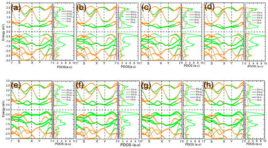
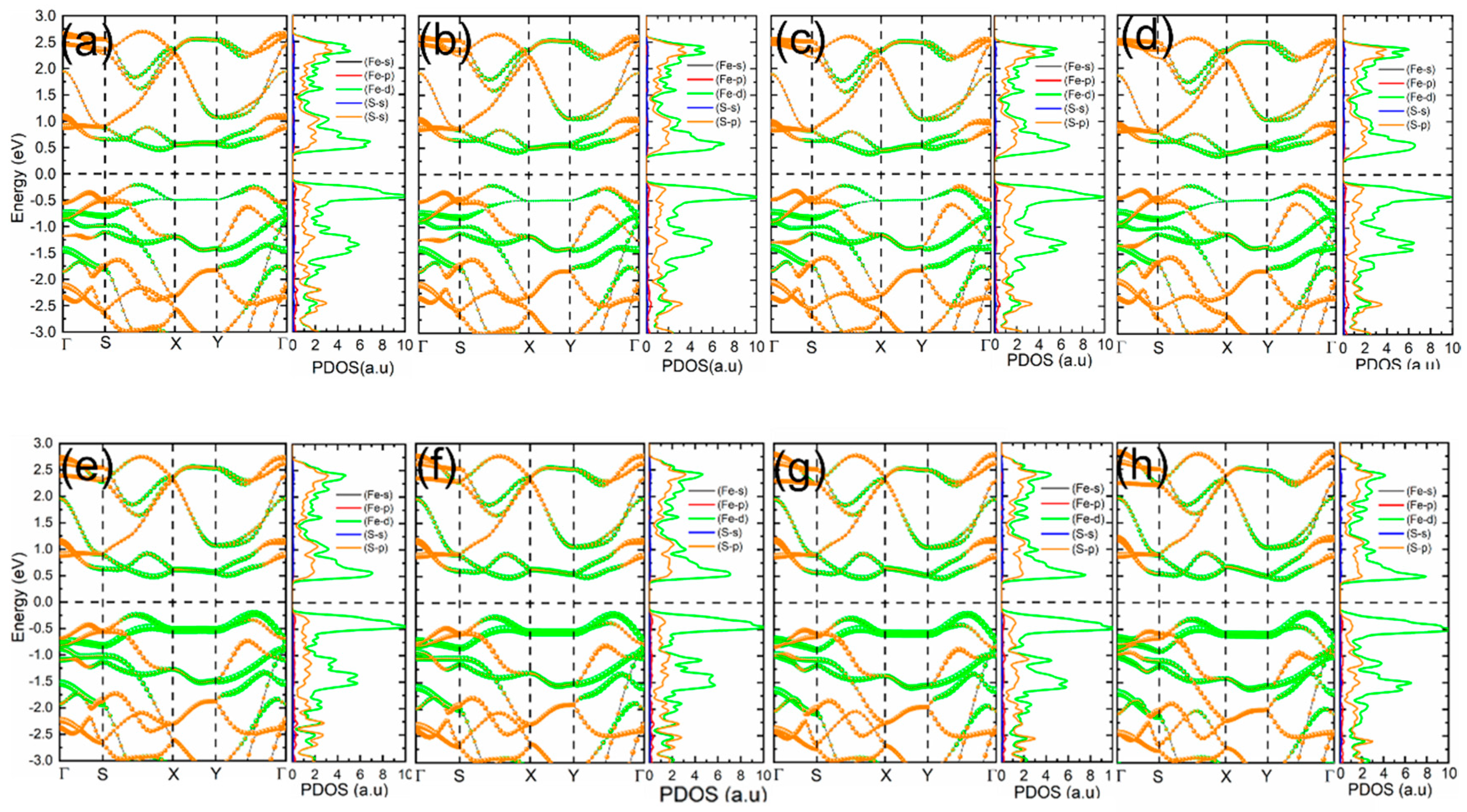
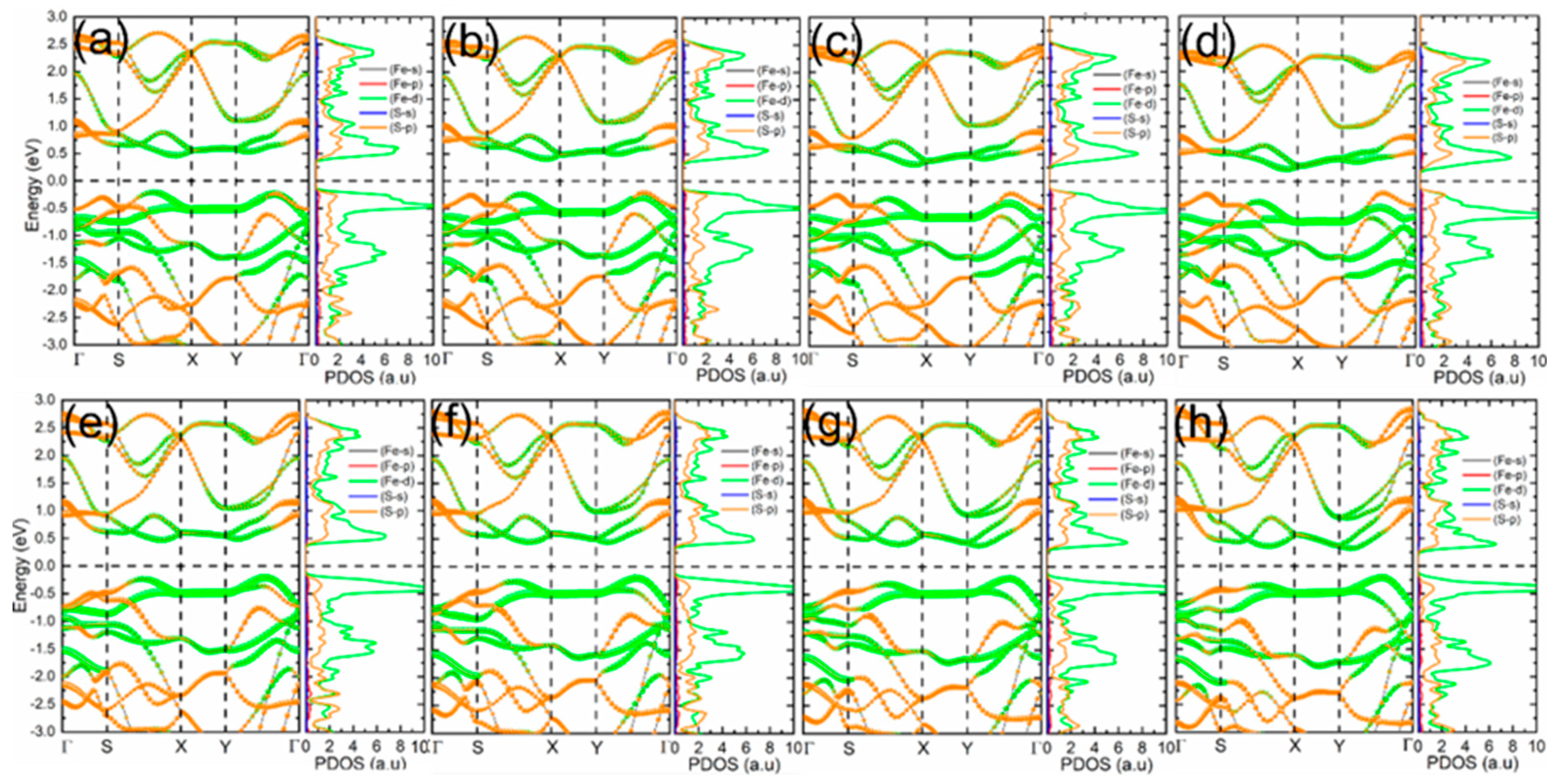
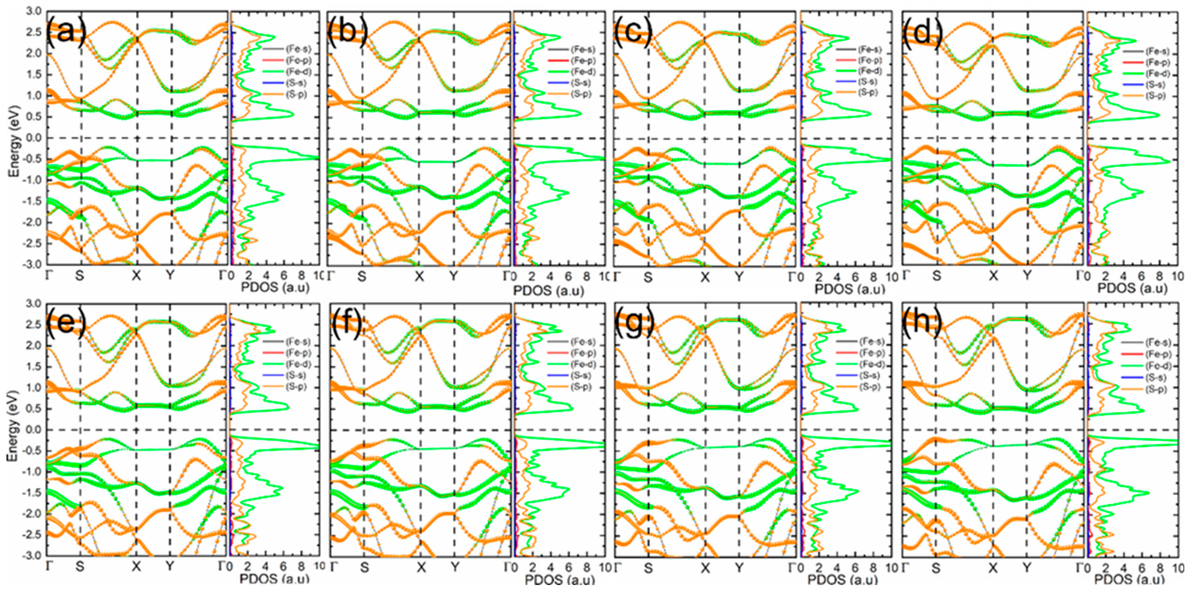
Because the 4 × 1 × 1 supercell can be mapped onto multiple equivalent primitive cell choices, it is important to confirm that the computed electronic structure is independent of this choice. The band structure and partial density of states were therefore recomputed using three alternative Brillouin zone representations, denoted C11, C12, and C22, corresponding to different but crystallographically equivalent cell orientations. All three representations yield an identical indirect bandgap of 0.70 eV with the same orbital character at the band edges, confirming that the results are not an artefact of a particular zone-folding choice, as shown in Figure 4, Figure 5 and Figure 6, respectively. These figures maintain the same orbital projection scheme: black (Fe-s), red (Fe-p), green (Fe-d), blue (S-s), and orange (S-p). Figure 4 (C11 representation) confirms the indirect bandgap of 0.70 eV, with the VBM at Γ dominated by S-p states and the CBM along Γ–X primarily from Fe-d. The pDOS shows the same valence bandwidth and orbital hierarchy: S-s deep in the valence band, Fe-d and S-p hybridized near the Fermi level, and Fe-d dominating the conduction band onset. Figure 5 (C12 representation) presents identical band topology and orbital character, with only slight visual differences in band folding due to the cell choice [7,27]. The distribution of the pDOS remains unchanged, thereby strengthening the electronic description. Again, a 0.70 eV indirect gap is obtained from Figure 6 (C22 representation), and the same characteristics for the pDOS are found: S-p dominates the upper valence band, Fe-d the lower conduction band, and there is little Fe-s, Fe-p, and S-s character near the gap edges.
Figure 4.
Electronic band structures and corresponding partial density of states (PDOS) of 1T′-FeS2 calculated using the C11 Brillouin-zone representation. Subfigures (a–h) display the electronic band structures (left panels) and the corresponding atom- and orbital-projected PDOS (right panels) along high-symmetry k-paths. The PDOS includes contributions from Fe-s (calculated but too small to be resolved at the present scale), Fe-p, Fe-d, S-s, and S-p orbitals.
Figure 5.
Electronic band structures and corresponding partial density of states (PDOS) of FeS2 calculated using the C12 Brillouin-zone representation. Subfigures (a–h) show the electronic band structures (left panels) along high-symmetry k-paths and the corresponding orbital-projected PDOS (right panels). The projected states are resolved into Fe-s (black; calculated but too small to be resolved at the present scale), Fe-p (red), Fe-d (green), S-s (blue), and S-p (orange) contributions.
Figure 6.
Electronic band structures and corresponding partial density of states (PDOS) of FeS2 calculated using the C22 Brillouin-zone representation. Subfigures (a–h) present the electronic band structures (left panels) along high-symmetry k-paths and the corresponding orbital-projected PDOS (right panels). The PDOS consists of contributions from Fe-s (black; calculated but too small to be resolved at the present scale), Fe-p (red), Fe-d (green), S-s (blue), and S-p (orange) orbitals.
It is instructive to compare with bulk pyrite. The band gap of the 3D crystal is 0.95 eV (experimental), or 0.83 eV (DFT-PBEsol), and the band gap has the same character as the 2D crystal but is wider because of the interlayer dispersion. The smaller monolayer gap is due to increased bonding energies and decreased anti-bonding energies caused by out-of-plane confinement; however, the distortion also counteracts this by increasing the in-plane hybridization energies. The Fermi level is close to the center of the gap, with the slightly higher density of Fe 3d states in the conduction band. This p-type pinning is consistent with defect chemistry in pyrite that posits that sulfur vacancies are donors, and that they are less common in the clean monolayer.
The electronic structure was further validated by computing the work function and ionization potential. The work function, defined as the energy difference between the vacuum level and the Fermi level, is 5.1 eV, suitable for interfacing with common electrodes. The ionization potential (energy to remove an electron from the VBM) is 5.8 eV, and the electron affinity (energy gained by adding an electron to the CBM) is 5.1 eV, yielding a transport gap of 0.7 eV, matching the band calculation. These values position 1T′-FeS2 as a moderate-bandgap semiconductor with balanced electron and hole injection barriers.
3.3. Strain Engineering of Bandgap and Electronic Properties
To investigate the effects of mechanical strain on the electronic structure, the 1T′-FeS2 monolayer was subjected to systematic mechanical strain. Strain was introduced by scaling the in-plane lattice vectors while keeping the spacing between the lattice planes in the vacuum direction fixed at 20 Å. They applied uniaxial strain either along the x-axis (longer a′ = 17.594 Å) or y-axis (shorter b′ = 3.20231 Å) and biaxial strain along both the x-axis and y-axis. Strain values ranged from 1 to −1, indicating tensile and compressive deformations, respectively. All atomic positions were fully relaxed at each strain level using the CASTEP code with the PBEsol functional, and ionic forces were kept below 0.01 eV/Å. This method accounts for both lattice distortion and internal structure response, which are essential for correctly predicting the band gap in 2D materials.
The evolution of the indirect bandgap under strain is summarized in Table 1. In the unstrained state, the bandgap is 0.70 eV. Under uniaxial strain along the x-axis, the bandgap decreases modestly: from 0.70 eV to 0.65 eV at −4% compression and to 0.56 eV at +4% tension. The response is, however, much stronger along the y-axis, which is the direction that is softer because the lattice constant is shorter and the atoms are more clustered. The gap narrows to 0.53 eV with a reduction in compressive strain to −4%, and decreases sharply to 0.44 eV with tensile strain of +4%, corresponding to a 37% reduction. The gap fluctuates between 0.62 eV (−4%) and 0.66 eV (+4%) under biaxial strain, indicating that the strain is balanced in both directions [24,28]. The stronger strain response along y relative to x is a direct consequence of the structural anisotropy of the 1T′ phase: the shorter equilibrium lattice constant b = 3.202 Å along y places Fe atoms in closer proximity, creating a stiffer but more electronically coupled bonding environment. Small deformations along y therefore produce larger changes in Fe–S bond length and Fe–S–Fe angle than equivalent deformations along the longer x-direction, directly amplifying the perturbation to the d–p orbital overlap that controls the band edges.
Table 1.
Strain-dependent structural and electronic properties of the 1T′-FeS2 monolayer under uniaxial and biaxial deformation.
The physical mechanism behind this bandgap modulation is revealed by analysis of band-edge shifts and orbital interactions. Figure 6 shows the band structure under +4% uniaxial tensile strain along the y-axis, which corresponds to the maximum bandgap reduction. Compared with the unstrained case (Figure 3), the conduction band minimum along the Γ–X direction decreases in energy by approximately 0.18 eV. In comparison, the valence band maximum at Γ rises by 0.08 eV, resulting in the net 0.26 eV closure. This is an asymmetric shift due to improved Fe–S bond stretching in the y-direction, which increases the Fe 3d bandwidth in the conduction band and increases d–p orbital overlap. On the other hand, when the compression is −4% along y, the CBM increases while the VBM decreases slightly, leaving the gap at 0.53 eV. The partial density of states under strain (shown in the right panels of Figure 5 and Figure 6) further confirms the Fe dominance of the CBM, and the S-p dominance of the VBM, with the density of states around the edges becoming more intense with tensile strain, as a result of the flattening of the bands [10].
The evolution of bond lengths under strain provides structural insight. In the unstrained state, the average Fe–S bond is 2.129 Å. Under +4% y-tensile strain, bonds along the deformation direction elongate to 2.21 Å, while perpendicular bonds contract slightly to 2.10 Å due to Poisson coupling. This differential stretching enhances d–p σ* antibonding character in the conduction band, lowering its energy [1]. Under compression, bonds shorten uniformly to 2.06 Å, reducing overlap and raising the CBM. The distorted 1T′ framework accommodates up to ±4% strain without lattice instability, as confirmed by real phonon frequencies at all strained geometries.
Effective masses also react to strain. The electron effective mass at the CBM drops to 0.72 m0 under +4% y-tensile strain, as the electron dispersion along Γ–X is increased, while the hole mass at Γ is increased to 2.6 m0 by the flattening of the valence bands. This improves n-type mobility under tension, which is advantageous for electron transport in strained devices. Similarly, the effective masses change by less than 10% under biaxial strain [26]. The dominance of the y-direction in bandgap modulation can be understood from the structural anisotropy of the 1T′ phase. Along the y-direction, the equilibrium lattice constant b = 3.202 Å is significantly shorter than a′ = 17.594 Å along x, and the 1T′ distortion concentrates Fe–Fe clustering along this direction. As a result, the Fe–S bonds aligned with y are shorter and more compressed at equilibrium, placing the d–p orbital coupling closer to its maximum sensitivity. As the Fe–S bond is stretched along y, the increment of the Fe–S bond length per unit strain is greater than that along x, thus directly improving the hybridization between Fe 3d and S 3p states at the band edges. This bond-length sensitivity is increased by the anisotropic nature of the ligand field in the distorted octahedral coordination environment, as the d_xy and d_x2 − y2 orbitals interact most strongly with the y-direction and thus are most susceptible to y-directional deformation.
The strain-gauge factor for bandgap sensitivity is calculated as GF = (ΔE_g/E_g)/ε. Along the y-direction, ΔE_g = −0.26 eV, E_g = 0.70 eV, ε = 0.04, yielding GF ≈ 9.3—significantly higher than silicon (~3) and comparable to top 2D strain sensors like MoS2 (~5–7). This high sensitivity arises from the soft lattice and strong d–p coupling in the 1T′ phase [24]. Compared with bulk FeS2, FeS2 slabs, and common 2D strain sensors, the present monolayer exhibits a much stronger strain-induced bandgap response, as summarized in Table 2 [29,30].
Table 2.
Strain-sensitive electronic properties of FeS2 and comparison with selected 2D materials.
The distorted 1T′ FeS2 monolayer shows a stronger bandgap response to strain than bulk FeS2 and common 2D strain-sensitive materials, while remaining dynamically and thermally stable. To ensure consistency across cell representations, strained band structures were recomputed in the C11, C12, and C22 mappings at selected strain levels. Table 2 shows +4% y-tensile strain in the C11 representation: the bandgap remains 0.44 eV, with identical edge states and orbital character. The same strain is present in C12 and C22 mappings, respectively, confirming that zone folding does not alter physical results [7]. The pDOS in each case shows enhanced Fe-d density in the lowered conduction band and S-p intensification near the raised VBM.
3.4. Optical Properties and Absorption Under Strain
The optical properties of the 1T′-FeS2 monolayer were evaluated by computing the frequency-dependent dielectric function ε(ω) = ε1(ω) + iε2(ω) within the random phase approximation (RPA), using a dense 24 × 24 × 1 k-point grid and 200 empty bands to ensure convergence of interband transitions. The absorption coefficient α(ω) was derived from the imaginary part of the dielectric function as
where c is the speed of light, all calculations included spin–orbit coupling and were performed in the three-cell representations (C11, C12, C22) to maintain consistency with the electronic structure analysis. The in-plane components (xx and yy) were averaged to account for the rectangular symmetry, and strain was applied as described in Section 3.3, with full ionic relaxation at each level [31].
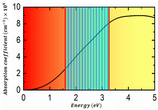
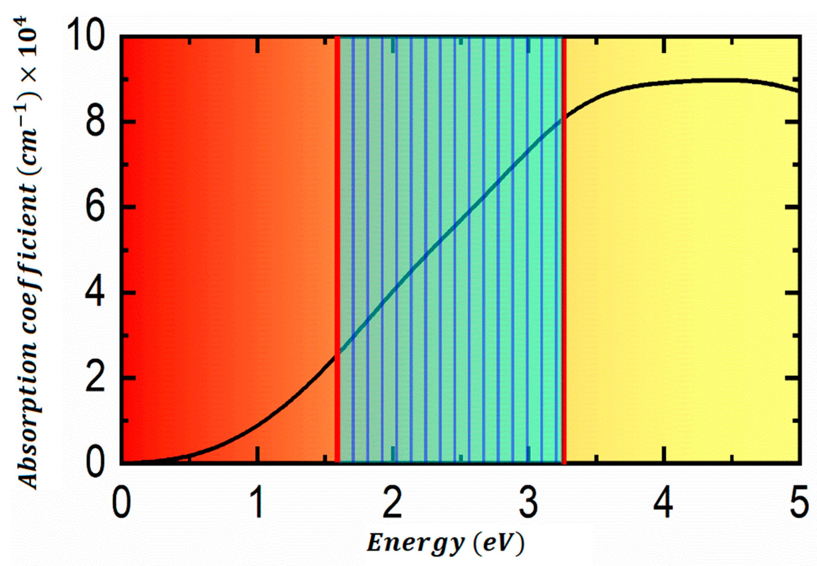
The unstrained absorption spectrum is shown in Figure 7. The onset of absorption occurs just above the indirect bandgap of 0.70 eV. Still, the first prominent peak—corresponding to direct transitions near the Γ point—appears at 2.5 eV, in excellent agreement with experimental optical data on FeS2 thin films and nanocrystals. The absorption coefficient rises sharply beyond this threshold, exceeding 104 cm−1 for photon energies above 2.8 eV and reaching 5 × 104 cm−1 at 4.0 eV. This high absorptivity stems from strong Fe 3d → Fe 3d and S 3p → Fe 3d transitions, enhanced by the high joint density of states in the distorted 1T′ phase. The spectrum is nearly isotropic in the unstrained state, with xx and yy components differing by less than 8% due to weak in-plane anisotropy.
Figure 7.
Optical absorption coefficient of the 1T′-FeS2 monolayer under strain. The unstrained monolayer is shown in black, the +4% tensile strain along the y-direction in red, and the −4% compressive strain along the y-direction in blue. Rredshift of the absorption peak under tensile strain (2.5 → 2.24 eV), and blueshift under compressive strain (2.5 → 2.69 eV). The inset shows the polarization-dependent absorption (xx vs. yy) under +4% y-tensile strain, highlighting strain-induced optical anisotropy.
The absorption edge redshifts by 0.26 eV, aligning with the bandgap reduction from 0.70 eV to 0.436 eV. The first peak shifts from 2.5 eV to 2.24 eV, and the overall spectrum extends to lower energies, with α(ω) > 104 cm−1 now starting at ~2.1 eV. This redshift arises from the lowered conduction-band minimum (Fe-d states) and an enhanced oscillator strength due to bond elongation and increased p–d overlap. The yy-polarized component (parallel to strain) shows a stronger redshift (0.29 eV) than xx (0.22 eV), introducing strain-induced optical anisotropy [32].
Under −4% compressive strain along the y-axis, the absorption edge blueshifts by 0.19 eV, consistent with the bandgap increase to 0.53 eV. The first peak moves to 2.69 eV, and the onset of strong absorption shifts above 2.4 eV. The yy component blueshifts more (0.22 eV) than xx (0.15 eV), again reflecting directional bond compression. The absorption magnitude remains high (>104 cm−1), but the spectrum is pushed to higher energies, reducing visible-light harvesting efficiency.
The spectral shift rate quantifies the strain-optical coupling:
This high sensitivity enables strain-tunable photodetectors with spectral response adjustable across the near-infrared to visible range.
The imaginary part of the dielectric function (ε2(ω)) confirms that the 2.5 eV peak originates from Γ-point transitions between S-p (VBM) and higher Fe-d states (~1.8 eV above CBM), not captured in the indirect gap. Strain modulates both the energy and oscillator strength of this transition: tensile strain increases ε2 by 12% at the peak, while compressive strain decreases it by 8%. The real part ε1(ω) shows the corresponding changes in refractive index, from n (2.5 eV) = 3.1 (unstrained) to 3.3 (+4% y) and 2.9 (−4% y).
Comparison with the experimental data is informative. Bulk pyrite exhibits a first absorption peak at ~2.4–2.6 eV [28,29], and FeS2 thin films show onsets near 1.0 eV with strong visible absorption. The computed monolayer results show an indirect onset at 0.7 eV and a direct peak at 2.5 eV, with α > 104 cm−1; this profile matches the data while eliminating defect-related sub-gap states common in bulk. The strain-induced red/blue shifts align with observations in mechanically deformed pyrite films, in which tensile bending reduces the effective gap [7].
3.5. Structural Stability: Phonons, Molecular Dynamics, and Cleavage Energy
The phonon dispersion and molecular dynamics results in Section 3.1 are presented in full quantitative detail, along with calculations of the elastic constants, which were not included in the overview of the structure. The optimized 1T′-FeS2 monolayer was comprehensively investigated for its structural stability to ensure its thermodynamic and dynamic feasibility. The phonon dispersion was computed within CASTEP using a 4 × 4 × 1 supercell and 4 × 4 × 1 k-points, with the finite displacement method employed. There are no imaginary frequencies in the entire Brillouin zone associated with this spectrum, further verifying dynamic stability. The highest optical mode is around 420 cm−1, where it is dominated by Fe–S stretching; the acoustic branches are linearly dispersive near Γ, thereby demonstrating the system’s elastic robustness.
Thermal stability was assessed through ab initio molecular dynamics (MD) in the NVT ensemble with a Nosé–Hoover thermostat. The system was simulated at 1000 K for 30 ps using a 1 fs time step. Atomic root-mean-square displacement (RMSD) remains below 0.4 Å, and the radial distribution function preserves sharp Fe–S (2.13 Å) and S–S (3.45 Å) peaks. No bond breaking, reconstruction, or phase transition occurs, demonstrating that the 1T′ structure is thermally stable well beyond typical device operating temperatures.
The feasibility of exfoliation from bulk pyrite was quantified via cleavage energy using slab models of increasing thickness (1–6 layers). The energy required to isolate one monolayer is 0.32 J/m2 lower than graphene from graphite (>0.4 J/m2) and comparable to MoS2 (0.27 J/m2). This low value, arising from weak interlayer van der Waals forces, indicates that mechanical or liquid-phase exfoliation from natural or synthetic pyrite is energetically favorable [29].
Under mechanical strain (±4% uniaxial and biaxial), phonon calculations show no imaginary modes, confirming strain-induced stability. Elastic constants extracted from energy-strain curves are C11 = 118 N/m, C22 = 142 N/m, C12 = 38 N/m, satisfying Born criteria (C11 + C22 > 2C12, C11C22 − C122 > 0). The y-direction is stiffer due to shorter equilibrium bond lengths, consistent with its stronger mechanical response during bandgap modulation.
4. Conclusions
The distorted 1T′-FeS2 monolayer has been systematically investigated using first-principles density functional theory with the CASTEP code and PBEsol functional, revealing its structural, electronic, optical, and mechanical properties. The optimized 4 × 1 × 1 supercell exhibits a symmetry-breaking distortion with Fe–S bond lengths of 2.129 Å and bond angles of 75.832° and 98.179°, lowering the energy by 0.18 eV per primitive unit cell and establishing the 1T′ phase as the ground-state configuration. Dynamical and thermal stability are confirmed via phonon dispersion and ab initio molecular dynamics up to 1000 K. The low cleavage energy (0.32 J/m2) indicates that mechanical or liquid-phase exfoliation from bulk pyrite is feasible, providing guidance for future experimental synthesis.
Electronically, the monolayer is an indirect-bandgap semiconductor (0.70 eV) with VBM at Γ dominated by S-p states and CBM along Γ–X dominated by Fe-d states. Strain engineering enables strong and anisotropic bandgap modulation: under +4% tensile strain along the soft y-direction, the gap reduces by 37% to 0.44 eV, while biaxial strain induces weaker variations. The strain-gauge factor along y reaches ≈9.43, highlighting the monolayer’s potential as a high-performance 2D strain sensor. Effective masses indicate high carrier mobilities, suitable for electronic applications.
Optically, the monolayer exhibits a high absorption coefficient (>104 cm−1), with the direct transition peak at 2.5 eV in agreement with experiments. Strain modulates the absorption edge (redshift under tension, blueshift under compression), enabling tunable spectral response across the near-infrared to visible range. These properties, combined with earth abundance and mechanical flexibility, suggest applications in flexible photodetectors, deformable solar cells, and strain-sensitive optoelectronic devices.
Overall, this study demonstrates that the 1T′-FeS2 monolayer is a mechanically robust, electronically tunable, and optically active material, with strong anisotropic response to strain, offering a promising platform for next-generation flexible electronics and optoelectronic devices. Future investigations may explore heterostructure design or surface functionalization to further tailor electronic and optical responses for device integration.
Author Contributions
Conceptualization, S.A. and Y.P. (Yang Ping); methodology, Y.P. (Yang Ping) and M.N.T.; software, H.Z.; validation, H.Z., S.B. and Z.Z.; formal analysis, M.N.T.; investigation, M.N.T.; resources, H.X. and Y.P. (Yinlong Pan); data curation, S.B.; writing—original draft preparation, M.N.T.; writing—review & editing, Z.Z. and N.A.; visualization, S.B. and Z.Z.; supervision, Y.P. and H.X.; project administration, Y.P. (Yinlong Pan); funding acquisition, Y.P. (Yinlong Pan). All authors have read and agreed to the published version of the manuscript.
Funding
This research was funded by Shenzhen Science and Technology Program (No. KCXFZ20240903092407009), Technology Research and Development Program of Power China Eco-Environmental Group Co., Ltd. (No. ST-ZB-ZC-JY-JS-2025-04, No. ST-WQ-ZC-JY-LGSW-2024-06 (KYLGLG2024Z002)), Key Technology Research and Development Program of Power Construction Corporation of China (No. DJ-ZDXM-2024-54).
Data Availability Statement
All data supporting the findings of this study are included within the article. Additional data are available from the corresponding author upon reasonable request.
Conflicts of Interest
Authors Yang Ping, Hao Xu and Zhenzhou Zhang are employed by Power China Eco-Environmental Group Co., Ltd. Authors Yinlong Pan and Heng Zhu are employed by Shenzhen Metasensing Technology Co., Ltd. The remaining authors declare that the research was conducted in the absence of any commercial or financial relationships that could be construed as a potential conflict of interest. The funders had no involvement in the study design, data collection, data analysis, data interpretation, the writing of this article, or the decision to submit it for publication.
References
- Goel, N.; Kumar, R. Physics of 2D Materials for Developing Smart Devices. Nano-Micro Lett. 2025, 17, 197. [Google Scholar] [CrossRef] [Scilit] [PubMed]
- Boland, C.S.; Sun, Y.; Papageorgiou, D.G. Bandgap Engineering of 2D Materials toward High-Performing Straintronics. Nano Lett. 2024, 24, 12722–12732. [Google Scholar] [CrossRef] [Scilit] [PubMed]
- Lee, J.; Yang, J. Advances in the synthesis and functionalization of two-dimensional iron sulfides for energy applications. MRS Energy Sustain. 2025, 12, 62–80. [Google Scholar] [CrossRef] [Scilit]
- Douglas, A.; Carter, R.; Oakes, L.; Share, K.; Cohn, A.P.; Pint, C.L. Ultrafine Iron Pyrite (FeS2) Nanocrystals Improve Sodium–Sulfur and Lithium–Sulfur Conversion Reactions for Efficient Batteries. ACS Nano 2015, 9, 11156–11165. [Google Scholar] [CrossRef] [Scilit] [PubMed]
- Zebarjad, M.; Jamali-Sheini, F.; Yousefi, R. Nanostructured FeS2 films: Influence of effective parameters on electrochemical deposition and characterization of physical properties. Ceram. Int. 2021, 47, 21969–21981. [Google Scholar] [CrossRef] [Scilit]
- Krishnamoorthy, A.; Herbert, F.W.; Yip, S.; Van Vliet, K.J.; Yildiz, B. Electronic states of intrinsic surface and bulk vacancies in FeS2. J. Phys. Condens. Matter 2013, 25, 045004. [Google Scholar] [CrossRef] [Scilit] [PubMed]
- Ren, J.-T.; Feng, Y.; Lü, H.-F. Magnetic and electronic properties of the TM-doped/adsorbed 1T-FeS2. J. Magn. Magn. Mater. 2025, 638, 173733. [Google Scholar]
- Xu, H.; Xu, Y. Strain Engineering of Anisotropic Electronic, Transport, and Photoelectric Properties in Monolayer Sn2Se2P4. Nanomaterials 2025, 15, 679. [Google Scholar] [CrossRef] [Scilit] [PubMed]
- Kim, J.; Jeong, J.; Min, K. Strain engineering in Ti2CX2/WS2 van der Waals heterostructures: First-principles calculations on mechanical robustness and bandgap tunability. J. Mater. Sci. Technol. 2025, 253, 166–178. [Google Scholar]
- Singh, N.J.; Basumatary, I.; Kolli, C.S.R.; Sahatiya, P. Current Trends and Emerging Opportunities for 2D Materials in Flexible and Wearable Sensors. Chem. Commun. 2025, 61, 11158–11186. [Google Scholar] [CrossRef] [Scilit] [PubMed]
- Srivastava, R.P.; Ranjan, P.; Kumar, M.; Katiyar, A. 2D materials in functional optoelectronics: Recent advances and future prospects. Nanotechnology 2025, 36, 392001. [Google Scholar] [CrossRef] [Scilit] [PubMed]
- Chen, S.; Gong, X.; Walsh, A.; Wei, S.-H. Defect physics of the kesterite thin-film solar cell absorber Cu2ZnSnS4. Appl. Phys. Lett. 2010, 96, 021902. [Google Scholar] [CrossRef] [Scilit]
- Xiao, P.; Fan, X.-L.; Liu, L.-M.; Lau, W.-M. Band gap engineering of FeS2 under biaxial strain: A first principles study. Phys. Chem. Chem. Phys. 2014, 16, 24466–24472. [Google Scholar] [CrossRef] [Scilit] [PubMed]
- Winiarski, M.J.; Zasada, J.; Samsel-Czekała, M. Strain effects on electronic structures of monolayer iron sulphide and selenide. Comput. Mater. Sci. 2018, 142, 372–376. [Google Scholar] [CrossRef] [Scilit]
- Prabhu, M.K.; David, P.; Guisset, V.; Martinelli, L.; Coraux, J.; Renaud, G. Reactive Molecular Beam Epitaxy Growth of a 1T-FeS2 Single-Layer–Atomic Structure, Moiré, and Decoupling via Intercalation. ACS Nano 2025, 19, 13941–13951. [Google Scholar] [PubMed]
- Qiu, G.; Xiao, Q.; Hu, Y.; Qin, W.; Wang, D. Theoretical study of the surface energy and electronic structure of pyrite FeS2 (100) using a total-energy pseudopotential method, CASTEP. J. Colloid Interface Sci. 2004, 270, 127–132. [Google Scholar] [PubMed]
- Zhang, H.; Dai, Y.-M.; Liu, L.-M. Novel monolayer pyrite FeS2 with atomic-thickness for magnetic devices. Comput. Mater. Sci. 2015, 101, 255–259. [Google Scholar]
- Friedrich, R.; Ghorbani-Asl, M.; Curtarolo, S.; Krasheninnikov, A.V. Data-driven quest for two-dimensional non-van der Waals materials. Nano Lett. 2022, 22, 989–997. [Google Scholar] [PubMed]
- Musari, A.A.; Joubert, D.P.; Olowofela, J.A.; Akinwale, A.T.; Adebayo, G.A. Ab initio study of phonon dispersion and thermodynamic properties of pure and doped pyrites. Eur. Phys. J. B 2017, 90, 254. [Google Scholar] [CrossRef] [Scilit]
- Beiranvand, R.; Mehrabi, V. Structural, electronic and optical properties of bulk and monolayer iron diselenide: A density functional study. Phys. Scr. 2021, 96, 065803. [Google Scholar] [CrossRef] [Scilit]
- Nair, G.K.R.; Ji, X.; Guo, D.; Zhu, C.; Xu, X.; Zheng, X.; Yang, X.; Cui, J.; Li, P.; Wang, X. 1T-FeS2: A new type of two-dimensional metallic ferromagnet. arXiv 2022, arXiv:2202.00252. [Google Scholar]
- Tabassam, M.N.; Shahzad, A.; Almunyif, A.A.; Ali, S.; Murtaza, S.; Shahid, M. Structural, mechanical, electronic, optical, and thermoelectric properties of Sr2XUO6 (X = Cr, Dy): A first principles investigation for photovoltaic applications. J. Phys. Chem. Solids 2025, 204, 112770. [Google Scholar] [CrossRef] [Scilit]
- Ahmad, N.; Eisa, M.H.; Khan, M.; Sun, X.; Alkaoud, A.M.; Narasimharao, K.; Shahzad, M. First-Principles Investigation of Co2+ and Mn2+ Doping in Mg2SnO4: Structural, Electronic, Optical, Thermodynamic, and Mechanical Properties for Advanced Phosphor Applications. Micro Nanostruct. 2025, 208, 208323. [Google Scholar]
- Azizi, F. Strain engineering of topological transitions in 2D materials: A multi-band approach. Sci. Rep. 2025, 15, 44367. [Google Scholar] [CrossRef] [Scilit] [PubMed]
- Doiron, C.F. Alternative Materials for Harnessing Symmetry and Topology in Thermal Light Sources for Thermophotovoltaics. Ph.D. Thesis, Rice University, Houston, TX, USA, 2020. [Google Scholar]
- Postorino, S.; Grassano, D.; D’Alessandro, M.; Pianetti, A.; Pulci, O.; Palummo, M. Strain-induced effects on the electronic properties of 2D materials. Nanomater. Nanotechnol. 2020, 10, 1847980420902569. [Google Scholar] [CrossRef] [Scilit]
- Nazar, M. DFT Study of Optoelectronic and Thermoelectric Properties of Halide Double Perovskite Rb2TlSbX2 (X = Cl, Br, I) for Solar Cell Applications. Sch. J. Eng. Technol. 2025, 4, 208–222. [Google Scholar]
- Roldán, R.; Castellanos-Gomez, A.; Cappelluti, E.; Guinea, F. Strain engineering in semiconducting two-dimensional crystals. J. Phys. Condens. Matter 2015, 27, 313201. [Google Scholar] [CrossRef] [Scilit] [PubMed]
- Zhang, R.; Cai, F.; Mo, Y.; Luo, Q.; You, C.; Zheng, H. The generation of acoustic multi-vortex beams using a phase-only holographic lens. J. Appl. Phys. 2024, 136, 083102. [Google Scholar]
- Dai, Z.; Liu, L.; Zhang, Z. Strain Engineering of 2D Materials: Issues and Opportunities at the Interface. Adv. Mater. 2019, 31, 1805417. [Google Scholar] [CrossRef] [Scilit] [PubMed]
- Yakovkin, I.; Petrova, N. Influence of the thickness and surface composition on the electronic structure of FeS2 layers. Appl. Surf. Sci. 2016, 377, 184–190. [Google Scholar]
- Sah, R.K.; Tang, H.; Shahi, C.; Ruzsinszky, A.; Perdew, J.P. Effect of strain on the band gap of monolayer MoS2. Phys. Rev. B 2024, 110, 144109. [Google Scholar]
- Xiang, H.; Xu, B.; Liu, J.; Xia, Y.; Lu, H.; Yin, J.; Liu, Z. Quantum spin Hall insulator phase in monolayer WTe2 by uniaxial strain. AIP Adv. 2016, 6, 095005. [Google Scholar] [CrossRef] [Scilit]

Disclaimer/Publisher’s Note: The statements, opinions and data contained in all publications are solely those of the individual author(s) and contributor(s) and not of MDPI and/or the editor(s). MDPI and/or the editor(s) disclaim responsibility for any injury to people or property resulting from any ideas, methods, instructions or products referred to in the content. |
© 2026 by the authors. Licensee MDPI, Basel, Switzerland. This article is an open access article distributed under the terms and conditions of the Creative Commons Attribution (CC BY) license.