


Abstract
Y-doped HfO2 ferroelectric thin films were fabricated via the sol–gel chemical solution deposition method. The effects of Y doping concentration, film thickness, and annealing temperature on the structure, morphology, and electrical properties were systematically investigated. The results demonstrate that doping concentration, film thickness, and annealing temperature can significantly regulate the crystalline phase composition. Appropriate doping, moderate film thickness, and suitable annealing temperature effectively stabilize the ferroelectric orthorhombic phase and suppress the monoclinic phase. The optimized film is obtained under the conditions of 4 mol% Y doping, a film thickness of 59.2 nm, and rapid thermal annealing at 600 °C, which exhibits the best crystallinity, dense and flat surface, and moderate oxygen vacancy concentration. The optimized sample shows a remnant polarization of 86.9 μC/cm2, a coercive field of 1.1 MV/cm, and a leakage current density as low as 9.77 × 10⁻⁶ A/cm2, representing the best ferroelectric performance. This study provides a reliable process and experimental basis for the preparation of high-performance HfO2-based ferroelectric thin films by the sol–gel method.
1. Introduction
Hafnium oxide-based ferroelectric thin films exhibit promising application potential in cutting-edge microelectronic devices such as ferroelectric memories, field-effect transistors, and micro-electro-mechanical systems (MEMS), owing to their high Curie temperature, compatibility with CMOS technology, wide thickness window, and excellent fatigue resistance [1,2]. Compared with conventional perovskite ferroelectric materials, HfO2-based films can maintain stable ferroelectricity at the nanoscale, which is highly consistent with the trend of device miniaturization and integration [3,4].
Studies have confirmed that the ferroelectricity of HfO2 originates from the metastable orthorhombic phase, which tends to transform into the thermodynamically stable non-ferroelectric monoclinic phase at room temperature [5]. The orthorhombic phase can be stabilized and the monoclinic phase suppressed through element doping (Y, La, Zr, Si, Al, etc.), strain engineering, and optimized thermal treatment, thereby enhancing ferroelectric performance [6,7,8]. Among these strategies, Y3+ doping can introduce oxygen vacancies and modulate lattice distortion via valence differences, effectively regulating the crystalline phase composition and serving as an effective approach to improve the ferroelectricity of HfO2 [9].
Table 1 summarizes the ferroelectric properties of partial Y-doped HfO2 thin films prepared via various fabrication processes reported in recent years. At present, physical deposition processes, including atomic layer deposition (ALD), pulsed laser deposition (PLD), and magnetron sputtering, generally suffer from high cost and complex procedures. In contrast, sol–gel chemical solution deposition (CSD) features simple equipment, convenient operation, low cost, and flexible composition control, making it suitable for low-cost and large-scale fabrication [10]. However, the synergistic mechanism of doping concentration, film thickness, and annealing temperature on phase evolution, microstructure, and ferroelectric properties of sol–gel derived Y-doped HfO2 thin films remains unclear, and systematic comparison and optimal process determination are still lacking [11]. Accordingly, in this work, HfO2 thin films with different Y doping concentrations, film thicknesses, and annealing temperatures were prepared via the sol–gel method. Using XRD, XPS, SEM, AFM, and electrical measurements, the influences of process parameters on crystalline phase composition, surface morphology, elemental chemical states, and oxygen vacancies were systematically revealed, and the optimal preparation conditions were determined. This work provides experimental and theoretical support for the application of low-cost and high-performance HfO2-based ferroelectric thin films and devices.
Table 1.
Summary of ferroelectric doped-HfO2 films and their electrical properties.
2. Materials and Methods
2.1. Materials
Hafnium acetylacetonate (C20H28HfO8, ≥97%), yttrium(III) acetylacetonate hydrate (C15H21O6Y·xH2O, ≥99.9%), propionic acid (C3H6O2, ≥99.5%) and acetone (C3H6O, ≥99%) were supplied by Shanghai Aladdin Biochemical Technology Co., Ltd. (Shanghai, China). Absolute ethanol (AR grade) was obtained from Sinopharm Chemical Reagent Co., Ltd. (Shanghai, China). Single-side polished p-type (100) Si wafers (0.001–0.005 Ω·cm, 500 ± 10 μm) were purchased from Suzhou Jingxi Electronic Technology Co., Ltd. (Suzhou, China). Deionized water (AR grade) was procured from Sichuan UP Ultra-Pure Technology Co., Ltd. (Chengdu, China).
2.2. Precursor Solution and Thin Film Preparation
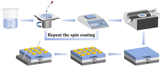
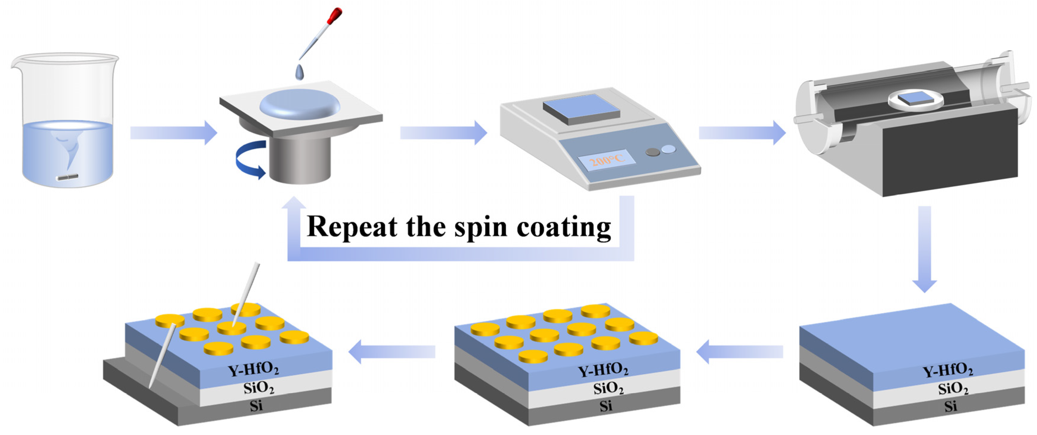
The preparation process of thin films is illustrated in Figure 1. In this work, thin films were fabricated via chemical solution deposition (CSD) owing to its simple equipment, facile operation, and low cost. Hafnium acetylacetonate and yttrium acetylacetonate were accurately weighed, with different amounts according to the designed doping concentrations, and dissolved in 10 mL of propionic acid. The mixture was heated and continuously stirred at 100–150 °C for 1–3 h until a homogeneous and transparent solution was obtained. Afterward, the solution was aged at room temperature for 7 days to obtain a homogeneous and stable precursor solution.
Figure 1.
Schematic diagram of the preparation process of Y-doped HfO2 thin films.
Heavily doped p-type Si wafers with a (100) orientation and dimensions of 1 × 1 cm2 were used as substrates. The wafers were ultrasonically cleaned in acetone to remove organic contaminants, rinsed with ethanol and deionized water, and then dried for subsequent use. Thin films were deposited onto the treated Si substrates by spin-coating. The substrates were first spin-coated at 500 rpm for 5 s, and then at 6000 rpm for 25 s. The as-deposited films were pre-annealed at 200 °C for 60 s to solidify the film layers. The spin-coating and pre-annealing cycles were repeated until the desired film thickness was achieved. Finally, all samples were treated by rapid thermal annealing (RTA) at 500–650 °C for 120 s in air to induce crystallization of the thin films. Table 2 lists the detailed preparation parameters of Y-doped hafnium oxide thin film samples.
Table 2.
Preparation parameters of Y-doped hafnium oxide thin film samples.
2.3. Thin Film Characterization
The crystal structure of the Y-doped HfO2 thin films was characterized by X-ray diffraction (XRD, Bruker D8 ADVANCE, Bruker Corporation, Billerica, MA, USA) over a scanning range of 20° to 50°. X-ray photoelectron spectroscopy (XPS, ESCALAB250Xi, Thermo Fisher Scientific Inc., Waltham, MA, USA) was employed to determine the elemental composition and chemical states in the Y-doped HfO2 films, with the adventitious C 1s peak at 284.8 eV used for calibration of the measured XPS spectra [17]. The surface and cross-sectional microstructures of the thin films were observed by field emission scanning electron microscopy (FE-SEM, Hitachi S-4800, Hitachi Ltd., Tokyo, Japan). The surface morphology of the Y-doped HfO2 thin films was investigated by atomic force microscopy (AFM, Bruker Dimension ICON, Bruker Corporation, Billerica, MA, USA) operated in tapping mode over a scan area of 1 × 1 μm2.
2.4. Electrical Measurement
For electrical characterization, a metal–ferroelectric–semiconductor (MFS) capacitor structure was adopted in this work. Top Au electrodes with an area of approximately 0.00785 cm2 were sputtered onto the film surfaces through a shadow mask using an ion sputtering system (ETD-800, Vision Precision Instruments, Beijing, China) for 3 min. Polarization–electric field (P–E) hysteresis and current density–electric field (J–E) measurements were carried out using a ferroelectric analyzer (PK-CPE1901, PolyK Technologies, LLC, State College, PA, USA). The frequency employed for dynamic hysteresis measurements was 1 kHz. All polarization values were normalized to the area of a single Au electrode.
3. Results and Discussion
3.1. XRD Analysis
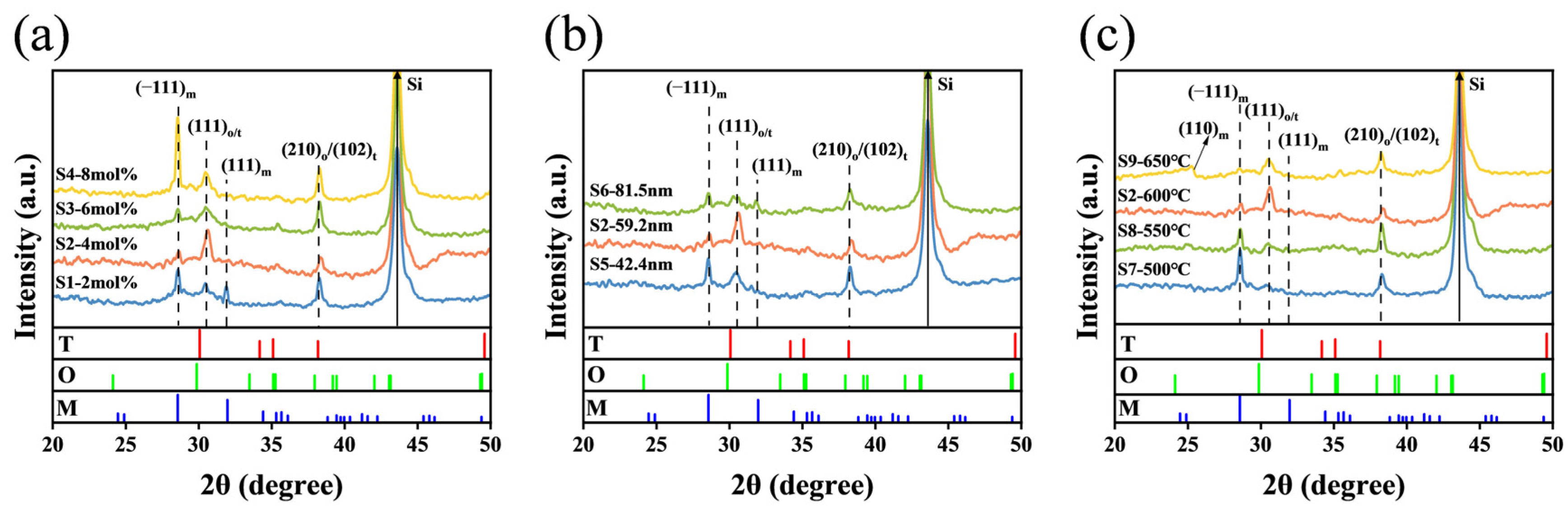
The notations m, o, and t represent monoclinic phase, ferroelectric orthorhombic phase, and tetragonal phase, respectively. Figure 2a displays the XRD patterns of samples with different Y doping concentrations. All thin films possess a measured thickness of approximately 59.2 nm and were annealed at 600 °C. Distinct diffraction peaks located at 28.5°, 30.5°, and 38.2° correspond to the (−111)m plane of the monoclinic phase, the mixed (111)o/t plane, and the mixed (210)o/(102)t plane, respectively. It is worth noting that the diffraction peaks of the orthorhombic and tetragonal phases highly overlap near 30.5°, making it impossible to fully separate the two phases and accurately quantify the orthorhombic fraction merely by the intensity of this overlapping peak. In contrast, all characteristic diffraction peaks belonging to the monoclinic phase can be clearly resolved. Therefore, the existence and relative content variation in the ferroelectric orthorhombic phase are verified by the evolution of monoclinic diffraction peaks and the macroscopic ferroelectric results. The 2 mol% Y-doped sample (S1) exhibits a characteristic (111)m diffraction peak near 32°. When the doping concentration increases to 4 mol% (S2), this peak completely disappears, and the intensity of the (−111)m peak at 28.5° is significantly reduced, indicating a decline in the monoclinic phase content. For Samples S3 and S4, further increasing the Y doping concentration gradually enhances the intensity of the (−111)m peak, suggesting the regrowth of the monoclinic phase. The ionic radius of Y3+ is 90 pm, while that of Hf4+ is 71 pm. Since Y3+ has a larger ionic radius than Hf4+, substitution of Hf4+ by Y3+ introduces tensile lattice distortion and lattice expansion. In addition, the substitution of tetravalent Hf4+ by trivalent Y3+ breaks charge neutrality and generates oxygen vacancies to compensate for the valence imbalance [9,18]. At a low Y doping concentration of 2 mol%, the tensile strain and oxygen vacancies introduced by doping are insufficient to fully stabilize the metastable ferroelectric orthorhombic phase, leaving abundant monoclinic phase inside the film. In contrast, excessively high doping concentrations of 6 mol% and 8 mol% lead to severe cumulative tensile distortion and aggregated oxygen vacancy clusters, which drastically reduce the phase transition energy barrier and drive the film to transform into the thermodynamically stable monoclinic phase.
Figure 2.
XRD patterns of (a) S1, S2, S3, and S4 samples with different Y doping concentrations, (b) S5, S2, and S6 samples with different film thicknesses, and (c) S7, S8, S2, and S9 samples with different annealing temperatures.
Figure 2b displays the XRD patterns of films with different thicknesses. All samples were doped with 4 mol% Y and annealed at 600 °C. Sample S5 (42.4 nm) shows the strongest diffraction peak of monoclinic phase at 28.5°, corresponding to the largest fraction of non-ferroelectric monoclinic phase; Sample S2 (59.2 nm) exhibits relatively high intensity of the overlapping (111)o/t diffraction peak at 30.5°, accompanied by suppressed monoclinic diffraction signals; Sample S6 (81.5 nm) features a reappeared (−111)m diffraction peak near 32°, indicating a remarkable rise in monoclinic phase content. This is because increased film thickness promotes grain growth and reduces grain boundary density. The stabilizing effect of strain and defects at grain boundaries on the ferroelectric orthorhombic phase is weakened. Accordingly, grains tend to transform into the thermodynamically more stable monoclinic phase, resulting in an elevated relative fraction of non-ferroelectric monoclinic phase [19,20].
Figure 2c illustrates the effect of annealing temperature on the phase composition of thin films. All samples were doped with 4 mol% Y and had a thickness of approximately 59.2 nm. Samples S7, S8 (500 °C, 550 °C) exhibit poor crystallinity and are mainly composed of the monoclinic phase. Sample S2 annealed at 600 °C achieves the optimal crystalline state, with the overlapping (111)o/t diffraction peak at 30.5 °C showing the highest intensity. Sample S9 (650 °C) shows a new (110)m diffraction peak at 25.2°, suggesting the regrowth of the monoclinic phase. This is because insufficient atomic migration occurs at low annealing temperatures, and the system preferentially forms the thermodynamically stable monoclinic phase. In contrast, excessively high temperature induces thermal relaxation of internal residual stress and accelerates grain coarsening, which weakens the lattice pinning effect of grain boundaries. With the dual constraints of strain and grain boundaries weakened, the metastable orthorhombic phase cannot be maintained, and the lattice spontaneously transforms into the low-energy and thermodynamically stable monoclinic phase [21,22].
3.2. XPS Analysis
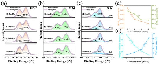
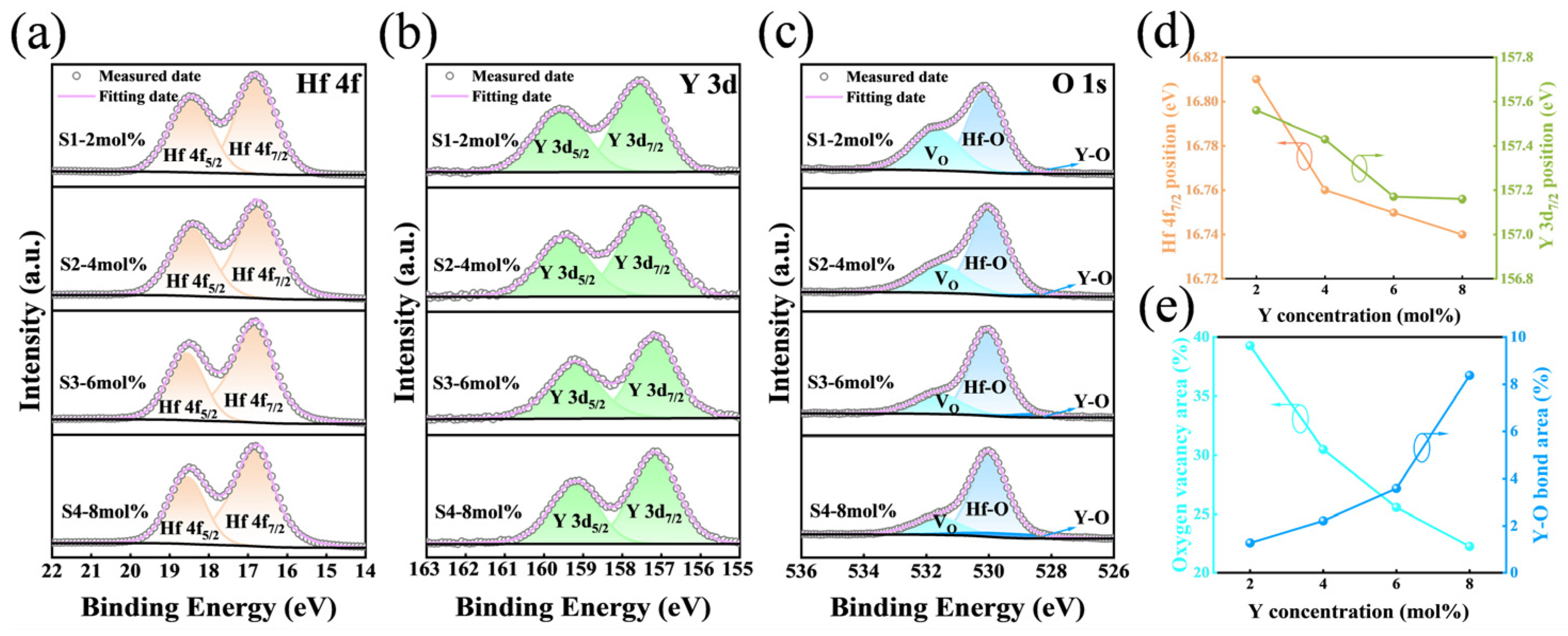
Figure 3a–c shows high-resolution XPS spectra of Hf 4f, Y 3d, and O 1s orbitals for S1, S2, S3, and S4 with varied Y doping contents. As plotted in Figure 3d, the core-level binding energies of Hf 4f and Y 3d shift negatively with increasing dopant concentration. The substitution of tetravalent Hf4+ by trivalent Y3+ produces excess free electrons, and doping-triggered oxygen vacancies trap localized electrons to raise the electron density surrounding Hf and Y atoms. Enhanced electron screening weakens nuclear attraction for inner core electrons, reducing binding energy and resulting in negative shifts in characteristic peaks [23].
Figure 3.
High-resolution XPS spectra: (a) Hf 4f, (b) Y 3d, and (c) O 1s orbitals of S1, S2, S3, and S4 samples. (d) Binding energy shifts in Hf 4f7/2 and Y 3d7/2 core levels for S1, S2, S3, and S4 samples. (e) Relative area percentages of oxygen vacancy and Y-O bond components derived from O 1s peak deconvolution for S1, S2, S3, and S4 samples.
The O 1s XPS spectrum is deconvoluted into three distinct peaks. The dominant peak near 530 eV is attributed to Hf-O bonds, the weak component around 528 eV verifies the formation of Y–O bonds, and the peak at approximately 532 eV corresponds to non-lattice oxygen predominantly derived from oxygen vacancies. The relative fractions of oxygen vacancies and Y–O bonds are quantified from the peak area ratios of the deconvoluted O 1s spectra. It is worth noting that this semi-quantitative evaluation possesses limited precision and only reveals the overall evolutionary trend of chemical states in the as-prepared films. As displayed in Figure 3e, the proportion of Y–O bonds gradually increases with elevated Y doping concentration, while the oxygen vacancy concentration exhibits an abnormal decreasing trend. For HfO2-based thin films, appropriate oxygen vacancies can reduce the lattice energy of high-symmetry phases (tetragonal and orthorhombic phases). These vacancies effectively stabilize the metastable ferroelectric orthorhombic phase at room temperature and suppress the phase transition toward the thermodynamically stable monoclinic phase, which serves as a fundamental prerequisite for acquiring superior ferroelectric performance. In contrast, excessive intrinsic oxygen vacancies aggravate lattice distortion and increase defect density, disrupting the long-range lattice order and deteriorating the structural stability of the ferroelectric o-phase [24]. Meanwhile, abundant defects tend to trigger abnormal grain growth and further modulate the phase composition of the films.
In this doped system, the as-prepared films inherently contain abundant excess intrinsic oxygen vacancies. The substitution of lattice Hf4+ by trivalent Y3+ induces an excess of negative charge within the lattice. To preserve overall charge neutrality, the system continuously consumes these pre-existing intrinsic oxygen vacancies. Furthermore, Y ions can occupy lattice defect sites and passivate oxygen vacancies, thereby inducing a continuous reduction in oxygen vacancy content with increasing doping concentration. When the oxygen vacancy concentration drops below the optimal range, its stabilization effect on the ferroelectric o-phase is significantly weakened [25]. As verified by the XRD patterns in Figure 2a, the diffraction intensities of metastable tetragonal and orthorhombic phases gradually decrease, whereas those of the monoclinic phase increase monotonically. Accordingly, the crystal structure spontaneously transforms into the monoclinic phase with the lowest thermodynamic free energy.
3.3. SEM and AFM Analysis
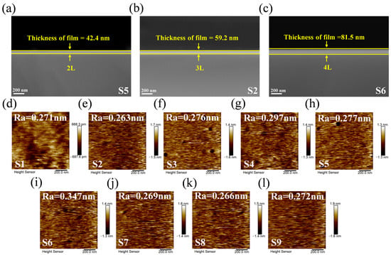
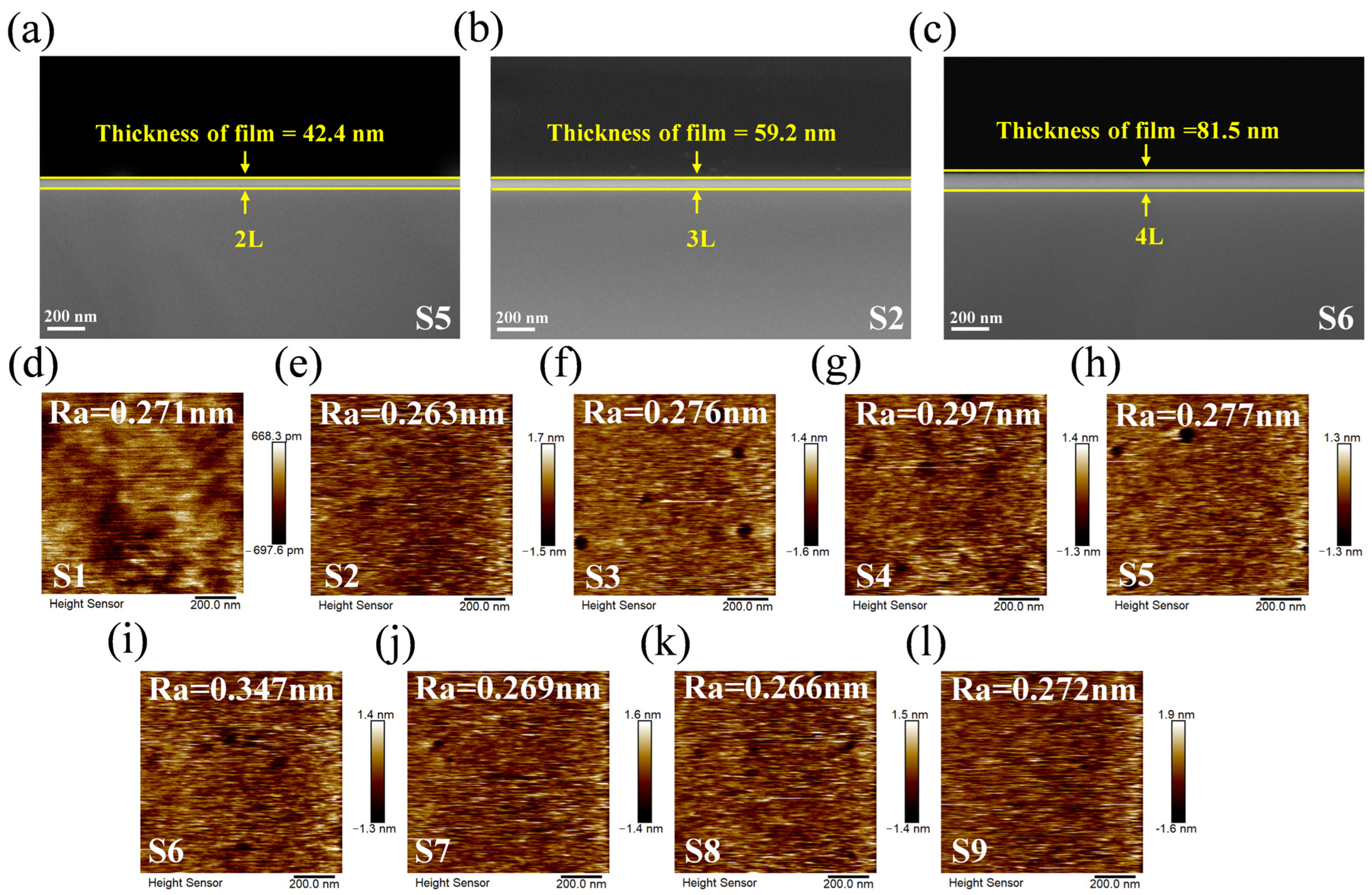
Figure 4a shows backscattered electron (BSE) cross-sectional SEM images of samples with different film thicknesses. The as-deposited films exhibit dense and continuous microstructures. The measured thicknesses corresponding to various spin-coating layers are listed below: 42.4 nm for S5 (2 layers), 59.2 nm for S2 (3 layers), and 81.5 nm for S6 (4 layers). It can be observed that film thickness increases with the number of spin-coating layers.
Figure 4.
Cross-sectional SEM images of thin-film samples with different thicknesses: (a) S5, (b) S2, and (c) S6. AFM images of thin-film samples under different preparation conditions: (d) S1, (e) S2, (f) S3, (g) S4, (h) S5, (i) S6, (j) S7, (k) S8, and (l) S9.
Figure 4d–l show AFM images of thin films under different preparation conditions. For samples S1–S4 (Y doping: 2 mol%, 4 mol%, 6 mol%, 8 mol%), the corresponding average surface roughness Ra reaches 0.271 nm, 0.263 nm, 0.276 nm, and 0.297 nm, respectively. All films possess Ra below 0.3 nm with smooth and pore-free surfaces, demonstrating favorable crystallinity and uniform grain distribution. Among them, sample S2 exhibits the minimum surface roughness. Moderate Y doping introduces oxygen vacancies to stabilize high-symmetry crystalline phases and suppress lattice distortion and volume expansion originating from phase transformation, whereas further doping leads to grain-boundary segregation of excess Y and local lattice distortion, gradually increasing surface roughness [26]. Samples S5, S2, and S6 with different film thicknesses (42.4 nm, 59.2 nm, 81.5 nm) show Ra values of 0.277 nm, 0.263 nm, and 0.347 nm. The remarkable roughness increase in sample S6 is attributed to accumulated interfacial defects and residual thermal stress derived from repeated spin-coating and annealing treatments [27]. Samples S7, S8, S2, and S9 (annealing temperature: 500 °C, 550 °C, 600 °C, 650 °C) display negligible roughness variation, and slight grain coarsening at 650 °C results in a modest rise in surface roughness.
3.4. Ferroelectric and Leakage Properties
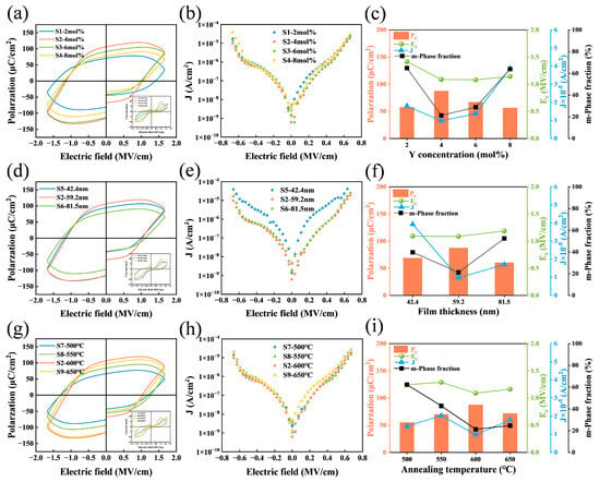
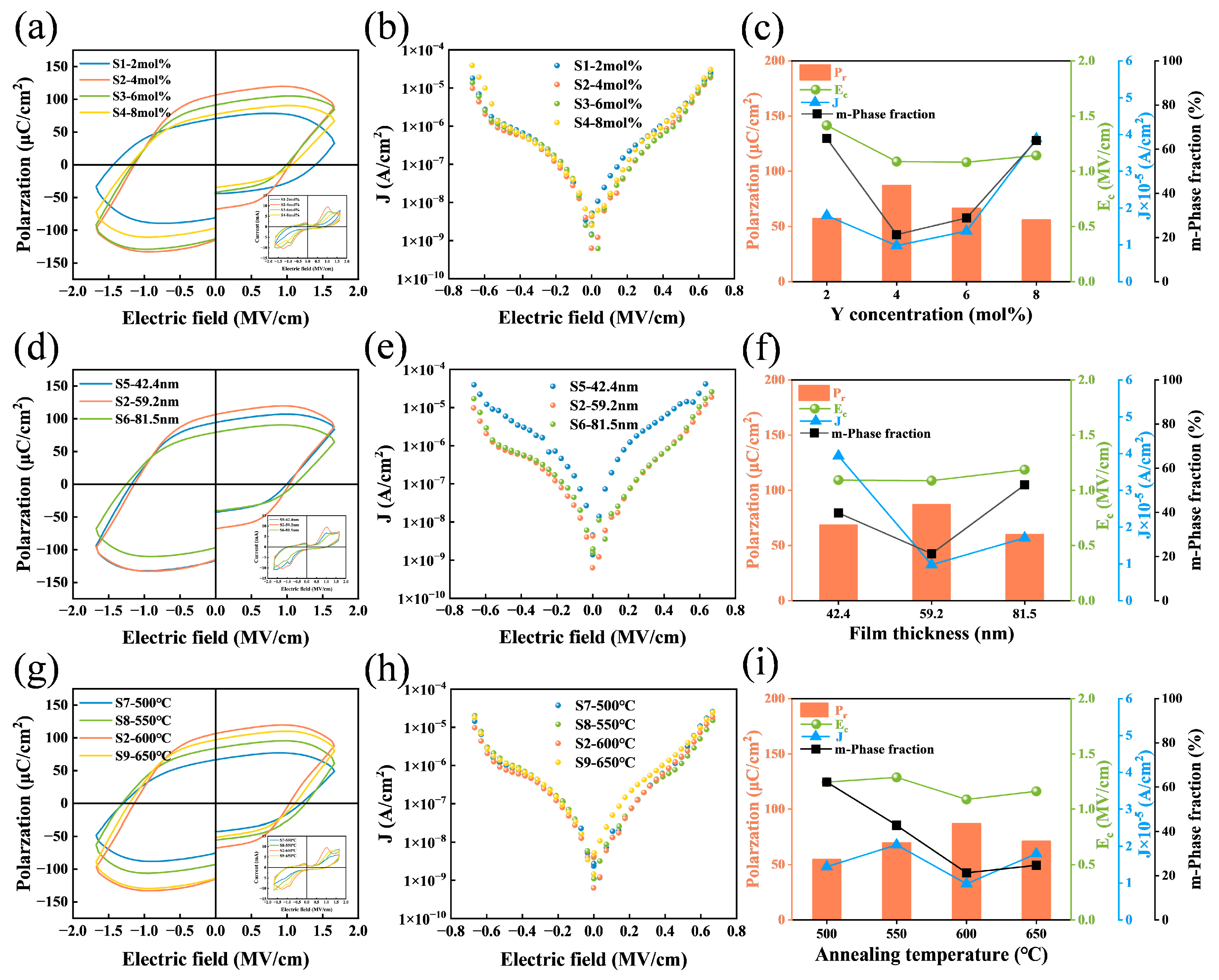
The electrical properties of Y-doped HfO2 films depend on their phase composition. The m-phase fraction and electrical parameters varying with Y doping concentrations are summarized in Figure 5c,f,i. The fraction of m-phase is calculated from XRD results by using the following formula [28]:
where I is the integrated intensity of the corresponding diffraction peak in XRD patterns, and the subscripts m and o/t refer to the monoclinic phase and orthorhombic/tetragonal phase, respectively.
m-phase fraction (%) = (I(−111)m + I(111)m)/(I(−111)m + I(111)m + I(111)o/t)
Figure 5.
P–E hysteresis loops (a,d,g), J–E leakage curves (b,e,h), and evolution of remnant polarization, coercive field, leakage current density, and monoclinic phase fraction (c,f,i). Rows from top to bottom correspond to varied Y doping concentrations, film thicknesses, and annealing temperatures, respectively.
Figure 5a,b display the P–E hysteresis loops and J–E curves of films with various Y doping concentrations. Combined with Figure 5c, the remnant polarization first increases and then decreases with rising Y content, while the monoclinic phase fraction declines initially and subsequently rises, showing an opposite variation trend to remnant polarization. Sample S2 (4 mol%) exhibits the lowest monoclinic phase fraction and optimal electrical performance, including the maximum remnant polarization of 86.9 μC/cm2, the minimum coercive field of 1.1 MV/cm, and the lowest leakage current density of 9.77 × 10⁻⁶ A/cm2. In contrast, the leakage current density increases to 3.88 × 10⁻⁵ A/cm2 for sample S4 with 8 mol% Y doping. Both insufficient and excessive doping deteriorate the remnant polarization and leakage characteristics. A low doping level fails to realize adequate lattice modulation for stabilizing the ferroelectric orthorhombic phase, while excessive Y doping induces dopant segregation and lattice distortion. These factors generate numerous defects and continuous conductive leakage paths, which ultimately impair the ferroelectric performance and elevate leakage current [29].
Figure 5d,e display the P–E hysteresis loops and J–E curves of films with various stacked thicknesses. Combined with Figure 5f, the remnant polarization first increases and then declines as the stacked thickness rises, while the monoclinic phase fraction decreases first and then increases. A slight enhancement of the coercive field is observed for sample S6 (81.5 nm). Sample S5 (42.4 nm) exhibits the maximum leakage current density of 3.93 × 10⁻⁵ A/cm2. Notably, compared with sample S2 (59.2 nm), thicker sample S6 possesses an elevated leakage current density of 1.70 × 10⁻⁵ A/cm2. Excessively thick stacked architectures introduce abundant interlayer interfaces and accumulated interfacial defects. These defects pin ferroelectric domain walls and restrain polarization switching, leading to increased coercive field; meanwhile, oxygen vacancies aggregated at interfaces construct continuous conductive leakage paths, which degrade remnant polarization and raise leakage current density [30].
Figure 5g,h present the P–E hysteresis loops and J–E curves of films with different annealing temperatures. Combined with Figure 5i, samples S7 (500 °C), S8 (550 °C), and S9 (650 °C) exhibit inferior ferroelectric and leakage properties and higher monoclinic phase content compared with S2 (600 °C), confirming that 600 °C is the optimal annealing temperature. Low annealing temperature restricts atomic diffusion, degrades crystallinity, and produces abundant intrinsic defects to impede the formation of ferroelectric orthorhombic phase; excessively high annealing temperature induces abnormal grain growth and excessive accumulation of oxygen vacancies. Both cases reduce remnant polarization and degrade leakage characteristics [31].
4. Conclusions
In this work, Y-doped HfO2 ferroelectric thin films were successfully fabricated via the sol–gel chemical solution deposition method. The influences of Y doping concentration, film thickness, and annealing temperature on the structure and performance of the films were systematically investigated. The results demonstrate that appropriate doping content, moderate film thickness, and suitable annealing temperature are crucial to stabilize the ferroelectric orthorhombic phase and suppress the thermodynamically stable monoclinic phase. The optimized sample prepared under the conditions of 4 mol% Y doping, a thickness of 59.2 nm, and rapid thermal annealing at 600 °C exhibits the best crystallinity, dense and uniform microstructure, smooth surface, moderate oxygen vacancy concentration, and excellent electrical properties, with a remnant polarization of 86.9 μC/cm2, a coercive field of 1.1 MV/cm, and a leakage current density as low as 9.77 × 10⁻⁶ A/cm2. According to the existing literature, the maximum remnant polarization of Y-doped HfO2 films is merely 50 μC/cm2 [14], which is lower than the value of 86.9 μC/cm2 obtained in this work, and the obtained film also delivers a smaller coercive field of 1.1 MV/cm. Nevertheless, the leakage current performance of the prepared films still has room for further improvement. This study can provide experimental reference and technical support for the preparation of high-performance HfO2-based ferroelectric thin films by the sol–gel method.
Author Contributions
R.L. is the first author of this work. T.J. conceived the idea and supervised the project. R.L., Y.C., and X.D. performed the series performance tests. Y.C. and X.D. assisted in data analysis. H.Z., J.W., X.H., and Y.L. provided research resource support. R.L. wrote the draft. Q.G. and T.J. reviewed and edited the manuscript. All authors have read and agreed to the published version of the manuscript.
Funding
This work was supported by the Ministry of Human Resources and Social Security of the People’s Republic of China (S20240022), Department of Science and Technology of Hubei Province (2023DJC051, 2023DJC062, 2025CDB021, 2025BCB085), the Hubei Provincial Natural Science Foundation for Innovation and Development (2025AFD325), and the Key Research and Development Program of Hubei Provincial (2023BCB072).
Data Availability Statement
The original contributions presented in this study are included in the article. Further inquiries can be directed to the corresponding author.
Acknowledgments
The authors gratefully acknowledge the Analytical and Testing Center of Hubei University for supplying testing equipment for this work. We also thank all group members for valuable discussions and experimental assistance throughout this study.
Conflicts of Interest
The authors declare no conflicts of interest. They have no known competing financial interests or personal relationships that could have appeared to influence the work reported in this paper.
References
- Chen, M.; Xiao, P.; Wang, X.; Cai, Y.; Zhao, H.; Wang, Y.; Guo, Q.; Jia, T. Effect of strain engineering on the ferroelectric properties of Hf0.5Zr0.5O2 films. Ceram. Int. 2025, 51, 16046–16051. [Google Scholar] [CrossRef] [Scilit]
- Li, G.; Liu, Y.; Yan, S.; Ma, N.; Xiao, Y.; Tang, M.; Long, Z.L. Charge-compensated co-doping stabilizes robust hafnium oxide ferroelectricity. J. Mater. Chem. C 2024, 12, 6257–6266. [Google Scholar] [CrossRef] [Scilit]
- Zhou, C.; Ma, L.; Feng, Y.; Kuo, C.-Y.; Ku, Y.-C.; Liu, C.-E.; Cheng, X.; Li, J.; Si, Y.; Huang, H.; et al. Enhanced polarization switching characteristics of HfO2 ultrathin films via acceptor-donor co-doping. Nat. Commun. 2024, 15, 2893. [Google Scholar] [CrossRef] [Scilit] [PubMed]
- Mehmood, F.; Alcala, R.; Vishnumurthy, P.; Xu, B.; Sachdeva, R.; Mikolajick, T.; Schroeder, U. Reliability improvement from La2O3 interfaces in Hf0.5Zr0.5O2-based ferroelectric capacitors. Adv. Mater. Interfaces 2023, 10, 2202151. [Google Scholar] [CrossRef] [Scilit]
- Ju, C.; Zeng, B.; Luo, Z.; Yang, Z.; Hao, P.; Liao, L.; Yang, Q.; Peng, Q.; Zheng, S.; Zhou, Y.; et al. Improved ferroelectric properties of CMOS back-end-of-line compatible Hf0.5Zr0.5O2 thin films by introducing dielectric layers. J. Mater. 2024, 10, 277–284. [Google Scholar] [CrossRef] [Scilit]
- Zeng, B.; Liu, C.; Dai, S.; Zhou, P.; Bao, K.; Zheng, S.; Peng, Q.; Xiang, J.; Gao, J.; Zhao, J.; et al. Electric field gradient-controlled domain switching for size effect-resistant multilevel operations in HfO2-based ferroelectric field-effect transistor. Adv. Funct. Mater. 2021, 31, 2011077. [Google Scholar] [CrossRef] [Scilit]
- Athle, R.; Persson, A.E.O.; Troian, A.; Borg, M. Top Electrode Engineering for Freedom in Design and Implementation of Ferroelectric Tunnel Junctions Based on Hf1−xZrxO2. ACS Appl. Electron. Mater. 2022, 4, 1002–1009. [Google Scholar] [CrossRef] [Scilit]
- Yajima, T.; Nishimura, T.; Migita, S.; Tanaka, T.; Uchida, K.; Toriumi, A. Regulating phase transformation kinetics via redox reaction in ferroelectric Ge-doped HfO2. Appl. Phys. Lett. 2020, 117, 182902. [Google Scholar] [CrossRef] [Scilit]
- Starschich, S.; Boettger, U. An extensive study of the influence of dopants on the ferroelectric properties of HfO2. J. Mater. Chem. C 2017, 5, 333–338. [Google Scholar] [CrossRef] [Scilit]
- Chen, H.; Chen, Y.; Tang, L.; Luo, H.; Zhou, K.; Yuan, X.; Zhang, D. Obvious ferroelectricity in undoped HfO2 films by chemical solution deposition. J. Mater. Chem. C 2020, 8, 2820–2826. [Google Scholar] [CrossRef] [Scilit]
- Li, S.; Zhou, D.; Shi, Z.; Hoffmann, M.; Mikolajick, T.; Schroeder, U. Involvement of unsaturated switching in the endurance cycling of Si-doped HfO2 ferroelectric thin films. Adv. Electron. Mater. 2020, 6, 2000264. [Google Scholar] [CrossRef] [Scilit]
- Müller, J.; Schröder, U.; Böscke, T.S.; Müller, I.; Böttger, U.; Wilde, L.; Sundqvist, J.; Lemberger, M.; Kücher, P.; Mikolajick, T.; et al. Ferroelectricity in yttrium-doped hafnium oxide. J. Appl. Phys. 2011, 110, 114113. [Google Scholar] [CrossRef] [Scilit]
- Starschich, S.; Griesche, D.; Schneller, T.; Waser, R.; Böttger, U. Chemical solution deposition of ferroelectric yttrium-doped hafnium oxide films on platinum electrodes. Appl. Phys. Lett. 2014, 104, 202903. [Google Scholar] [CrossRef] [Scilit]
- Olsen, T.; Schröder, U.; Müller, S.; Krause, A.; Martin, D.; Singh, A.; Müller, J.; Geidel, M.; Mikolajick, T. Co-sputtering yttrium into hafnium oxide thin films to produce ferroelectric properties. Appl. Phys. Lett. 2012, 101, 082905. [Google Scholar] [CrossRef] [Scilit]
- Mimura, T.; Shimizu, T.; Funakubo, H. Ferroelectricity in YO1.5-HfO2 films around 1 μm in thickness. Appl. Phys. Lett. 2019, 115, 032901. [Google Scholar] [CrossRef] [Scilit]
- Yun, Y.; Buragohain, P.; Li, M.; Ahmadi, Z.; Zhang, Y.; Li, X.; Wang, H.; Li, J.; Lu, P.; Tao, L.; et al. Intrinsic ferroelectricity in Y-doped HfO2 thin films. Nat. Mater. 2022, 21, 903–909. [Google Scholar] [CrossRef] [Scilit] [PubMed]
- Ansari, E.; Martinolli, N.; Hartmann, E.; Varini, A.; Stolichnov, I.; Ionescu, A.M. Vanadium-doped hafnium oxide: A high-endurance ferroelectric thin film with demonstrated negative capacitance. Nano Lett. 2025, 25, 2702–2708. [Google Scholar] [CrossRef] [Scilit] [PubMed]
- Liu, L.; Jiang, C.; Yuan, X.; Zhang, Y.; Chen, H.; Zhang, D. Large ferroelectric polarization and high dielectric constant in HfO2-based thin films via Hf0.5Zr0.5O2/ZrO2 nanobilayer engineering. J. Mater. 2025, 11, 100922. [Google Scholar] [CrossRef] [Scilit]
- Yin, L.; Li, X.; Xiao, D.; He, S.; Zhao, Y.; Peng, Q.; Yang, Q.; Liu, Y.; Wang, C. Improved ferroelectricity and endurance in Ca doped Hf0.5Zr0.5O2 films. Ceram. Int. 2024, 50, 49577–49586. [Google Scholar] [CrossRef] [Scilit]
- Zhou, Y.; Xiong, K.; Wu, S.; Tu, L.; Wang, X.; Chen, Y.; Wu, S.; Zeng, J.; Zheng, Y.; Gu, S.; et al. Anomalous polarization-switching phenomena and noteworthy pyroelectricity in ferroelectric Hf0.5Zr0.5O2 polycrystalline films. Mater. Today Phys. 2024, 43, 101414. [Google Scholar] [CrossRef] [Scilit]
- Mandal, B.; Valle, N.; Adib, B.E.; Girod, S.; Menguelti, K.; Fleming, Y.; Grysan, P.; Defay, E.; Glinsek, S. Control of Ferroelectricity in Solution-Processed Hafnia Films Through Annealing Atmosphere. Adv. Electron. Mater. 2024, 10, 2300893. [Google Scholar] [CrossRef] [Scilit]
- Liao, J.; Dai, S.; Peng, R.C.; Yang, J.; Zeng, B.; Liao, M.; Zhou, Y. HfO2-based ferroelectric thin film and memory device applications in the post-Moore era: A review. Fundam. Res. 2023, 3, 332–345. [Google Scholar] [CrossRef] [Scilit] [PubMed]
- Han, R.; Hong, P.; Ning, S.; Xu, Q.; Bai, M.; Zhou, J.; Li, K.; Liu, F.; Shi, F.; Luo, F.; et al. The effect of stress on HfO2-based ferroelectric thin films: A review of recent advances. J. Appl. Phys. 2023, 133, 240702. [Google Scholar] [CrossRef] [Scilit]
- Yasmeen, S.; Ryu, S.W.; Lee, S.H.; Lee, H. Atomic layer deposition beyond thin film deposition technology. Adv. Mater. Technol. 2023, 8, 2200876. [Google Scholar] [CrossRef] [Scilit]
- Shi, S.; Xi, H.; Cao, T.; Lin, W.; Liu, Z.; Niu, J.; Lan, D.; Zhou, C.; Cao, J.; Su, H.; et al. Interface-engineered ferroelectricity of epitaxial Hf0.5Zr0.5O2 thin films. Nat. Commun. 2023, 14, 1780. [Google Scholar] [CrossRef] [Scilit] [PubMed]
- Zhang, W.; Sun, N.; Zhou, D. Effect of Y2O3 interlayer on the electric properties of Y-doped HfO2 film deposited by chemical solution deposition. Ceram. Int. 2023, 49, 7670–7675. [Google Scholar] [CrossRef] [Scilit]
- Tian, Y.; Zhou, Y.; Zhao, M.; Ouyang, Y.; Tao, X. Effect of Ce doping on ferroelectric HfO2 from first-principles: Implications for ferroelectric thin films and phase regulation. J. Solid State Chem. 2023, 328, 124316. [Google Scholar] [CrossRef] [Scilit]
- Cheng, X.; Zhou, C.; Lin, B.; Yang, Z.; Chen, S.; Zhang, K.H.; Chen, Z. Leakage mechanism in ferroelectric Hf0.5Zr0.5O2 epitaxial thin films. Appl. Mater. Today 2023, 32, 101804. [Google Scholar] [CrossRef] [Scilit]
- Li, Y.C.; Li, X.X.; Wu, M.K.; Cui, B.-Y.; Wang, X.-P.; Huang, T.; Gu, Z.-Y.; Ji, Z.-G.; Yang, Y.-G.; Zhang, D.W.; et al. Dual Al2O3/Hf0.5Zr0.5O2 stack thin films for improved ferroelectricity and reliability. IEEE Electron Device Lett. 2022, 43, 1235–1238. [Google Scholar] [CrossRef] [Scilit]
- Schroeder, U.; Park, M.H.; Mikolajick, T.; Hwang, C.S. The fundamentals and applications of ferroelectric HfO2. Nat. Rev. Mater. 2022, 7, 653–669. [Google Scholar] [CrossRef] [Scilit]
- Xu, Y.; Yang, Y.; Zhao, S.; Gong, T.; Jiang, P.; Lv, S.; Yu, H.; Yuan, P.; Dang, Z.; Ding, Y.; et al. Robust breakdown reliability and improved endurance in Hf0.5Zr0.5O2 ferroelectric using grain boundary interruption. IEEE Trans. Electron Devices 2021, 69, 430–433. [Google Scholar] [CrossRef] [Scilit]

Disclaimer/Publisher’s Note: The statements, opinions and data contained in all publications are solely those of the individual author(s) and contributor(s) and not of MDPI and/or the editor(s). MDPI and/or the editor(s) disclaim responsibility for any injury to people or property resulting from any ideas, methods, instructions or products referred to in the content. |
© 2026 by the authors. Licensee MDPI, Basel, Switzerland. This article is an open access article distributed under the terms and conditions of the Creative Commons Attribution (CC BY) license.