


Abstract
Historically, TEM prep has been an artisan craft without a systematic workflow that ensures quantified control over TEM sample thickness. Over- and under-thinning is a significant problem in the TEM prep process. A direct measurement process was demonstrated to control the final thickness of the TEM lamella. Final lamella thickness was controlled by directly measuring lamella thickness in real time using a 10–15 kV SEM while performing secondary electron imaging at the mill position, allowing for (human-mediated) closed-loop processing. We demonstrated the utility of this technique by systematically thinning five TEM samples to discretely target thicknesses ranging from 100 nm down to 28 nm. We demonstrated the repeatability and simplicity of the process by fabricating 10 STEM lamella with a targeted thickness of 32 nm. We demonstrate the ability to fabricate an engineered multi-layered structure that acts as a lamella thickness measurement feature that is independent of sample type, allowing a broader implementation of in-line lamella thickness monitoring. We applied our thickness measurement technique to three thin-film materials (Au, Ag, and Cu) to obtain TEM lamella thickness target values needed to achieve electron transparency for each material. Having knowledge of a target thickness parameter prevents the over- and under-thinning problem in TEM prep.
1. Introduction
In the semiconductor field, transmission electron microscopy (TEM) analysis is a critical bottleneck to the development of the next generation of electronics. The typical TEM sample prep workflow has been evolving for the last 40 years to meet the needs of the industry [1,2,3,4,5,6]. Even after all the progress, it is still largely considered an artisan profession with many workflows highly dependent upon technician discretion. A problem in TEM prep is the lack of a well-known technique that enables quantified control over the final TEM lamella thickness.
Manual processing of TEM samples is slow but can also be precise and accurate when a skilled technician is used [7]. A problem that manual technicians face when processing TEM samples is that there is no real-time knowledge for lamella thickness while final thinning. This causes repeatability issues and, at times, useless data. The process to identify features and to manually isolate them is slow and error-prone. By comparing top-down SEM images of the site prior to processing with frontside and backside endpoint images of the TEM lamella, the thickness of the lamella can be estimated. This is effective when there is prior information known about sample geometry, but without this information, and in the case of trenches, samples with overburden material, or thin films, no such information is available, and the technician must process blindly. In these occurrences, the manual technicians simply thin to a predetermined stopping point, usually when the protective cap is depleted or when the sample warps. Ultimately, the problem is that manual technicians do not have numerical feedback during TEM sample thinning.
One strategy for manual TEM sample processing that has been implemented in the past is to use FIB mill marks to indicate the location of the feature of interest. In this workflow, the technician FIB marks near the AOI while on the bulk sample prior to TEM lift-out and then manually isolates the FIB marks during the TEM lamella final thinning. The FIB resolution limits both the feature size that can be fabricated (limited minimum width) and the positioning accuracy of the FIB feature relative to the area of interest. A FIB generally cannot fabricate mill lines much narrower than 15 nm [8]. The dynamic size of the FIB spot used for FIB marking introduces unreliability into this technique.
Automation of TEM sample processes is starting to take root with many tool manufacturers [9,10,11,12,13,14,15], including Thermo Scientific, Tescan, Carl Zeiss, and Hitachi, introducing some form of TEM prep automation software with newer systems. An automated dual-beam system can take a lamella from the bulk sample to a lamella on a TEM grid thinned down to approximately 100 nm within an hour. This is comparable to manual technician workflow. This process is largely blind in regard to centering a structure, deskewing a structure’s rotation, and isolating the structure to an arbitrary lamella thickness. To move to the next level, manufacturers will need to enact some sort of feedback for multiple steps in the lamella fabrication process. Manufacturers have started to implement feedback into the final thinning process for TEM processing using BSE thickness analysis or image recognition software for endpoint detection [16]; however, it is still in its early days, expensive, and not widely implemented. There is currently no accepted and widely adopted technique for closed-loop lamella processing.
In both lamella prep methods, manual or automated, the thinning problem is reduced to isolating the area of interest in the center of the lamella. To isolate a feature in the center of a lamella, one must know where the AOI is and where both the front- and back-cut faces of the lamella are relative to the AOI. This is complicated by uncertainty in the milled position, which partially arises from the dynamic size of the FIB milling spot. The FIB has a digital position of where it performed the last cut, but there is uncertainty in the exact physical position of the cut face relative to the AOI due to the dynamic width of the FIB spot size, which is unknown to the technician and only approximated by the system.
Lamella thickness evaluation has been performed using energy dispersive X-ray spectroscopy (EDXs), backscatter electron (BSE) monitoring, electron energy loss (EELs) spectroscopy, intensity calibration of secondary electron (SE) detectors, and post-analysis cross-sectional milling of the lamella window [17,18,19,20,21,22,23,24,25,26,27,28]. X-ray analysis, intensity-calibrated SE, and BSE can be performed while the TEM sample is being fabricated. These techniques require expensive equipment, they are highly material-dependent and require routine calibrations, and the signal changes with time as the detector degrades. Additional issues with SE intensity calibrations are that the secondary electron signal is not independent of the sample material (insulator, conductor, and semiconductor), SEM alignments, vacuum quality, working distance, and stage tilt, and the stage rotation relative to the detector can cause shadowing. While BSE intensity calibrations suffer from similar issues, additionally, they are material-dependent and require high current due to poor electron detection efficiency of BSE-biased detectors, and long dwell times can increase electron dose. In regard to EELs and post-cross-sectional analysis, these techniques lack the real-time feedback needed to control lamella thickness. To recap, the semiconductor industry has not standardized on any one TEM lamella thickness monitoring process due to the challenges described above.
As of today, 3D reconstruction of a TEM lamella has not yet been found in literature despite the author’s best efforts to find it. The precision needed to map the surfaces of a TEM lamella would need to be in the single-nanometer range [29,30,31,32,33]. If implemented using stereo vision, correspondence between the FIB image and SEM could be used; however, the FIB image quality could prevent sufficient resolution for SEM–FIB image comparison. Stereo reconstruction using two or more SEM images would need a stage tilt to capture separate perspectives, which would significantly slow thinning workflow. Both stereo reconstruction and generalizing to multi-image reconstruction, we find that these techniques are highly dependent on matching features, which require high-resolution images, and unique structures on a sample surface. These conditions are not compatible with an efficient TEM sample processing workflow. Further, most lamella-milled surfaces are bulk silicon, which lack unique structure for feature identification and 3D reconstruction. Intentional SEM or FIB patterning of surfaces could resolve some of these limitations, but this has not been attempted.
In this paper, we demonstrate a novel technique to measure and control the final lamella thickness using a 10–15 kV SEM with secondary electron imaging. We validate the technique by comparing tilted SE SEM images with cross-sectioned images of the lamella. We compare SE images obtained with various accelerating voltages 2–15 kV and find that 10–15 kV images produce accurate lamella thickness measurements. We compare SE images with bright-field and dark-field STEM images and find that the SE images can differentiate between the metal layer and the lamella thickness, while the STEM images could not. We engineer a modular multi-layer solution for lamella thickness monitoring that can be applied to many sample types, allowing broader implementation. We demonstrate the accuracy of the process by targeting discrete thickness targets for five TEM lamella. We demonstrate the repeatability, simplicity, and precision of the process by fabricating 10 TEM lamella with a 32 nm target thickness. We demonstrate an application of our thickness monitoring process to obtain target thicknesses for various thin-film materials.
2. Materials and Methods
2.1. Experiment and Technique
The experiment was broken into four phases to evaluate various subsets of the thinning workflow. Each phase is summarized below.
Experimental phase #1 was used to obtain SEM imaging conditions to measure lamella thickness using secondary electrons. For this lamella, we imaged with different accelerating voltages and compared STEM images versus SE images. This experimental phase included the fabrication of a multi-layered engineered structure that was independent of the sample surface. To implement this, we embedded a metal layer in the lamella’s protective cap that was able to be measured and correlated with lamella thickness.
Experimental phase #2 was used to demonstrate the ability to control the lamella thickness by fabricating a series of targeted thickness TEM lamella windows, with each lamella window having a different target thickness. These windows were cross-sectioned to validate thicknesses. The goal of this experiment was to demonstrate control over lamella thickness.
Experimental phase #3 was used to demonstrate simplicity and repeatability of the final thinning process. In total, 10 TEM windows were fabricated with a target thickness of 32 nm. These samples were cross-sectioned to validate lamella thickness. This approach for evaluating the repeatability of a lamella thickness monitoring technique directly reproduces repeatability results found in Tsurusawa et al. [10]. In their paper, they implement a calibrated BSE lamella thickness monitoring technique. To demonstrate repeatability, they fabricated eight TEM lamella with targeted thicknesses less than 18 nm. In this paper, they used EELs to characterize the final lamella thickness.
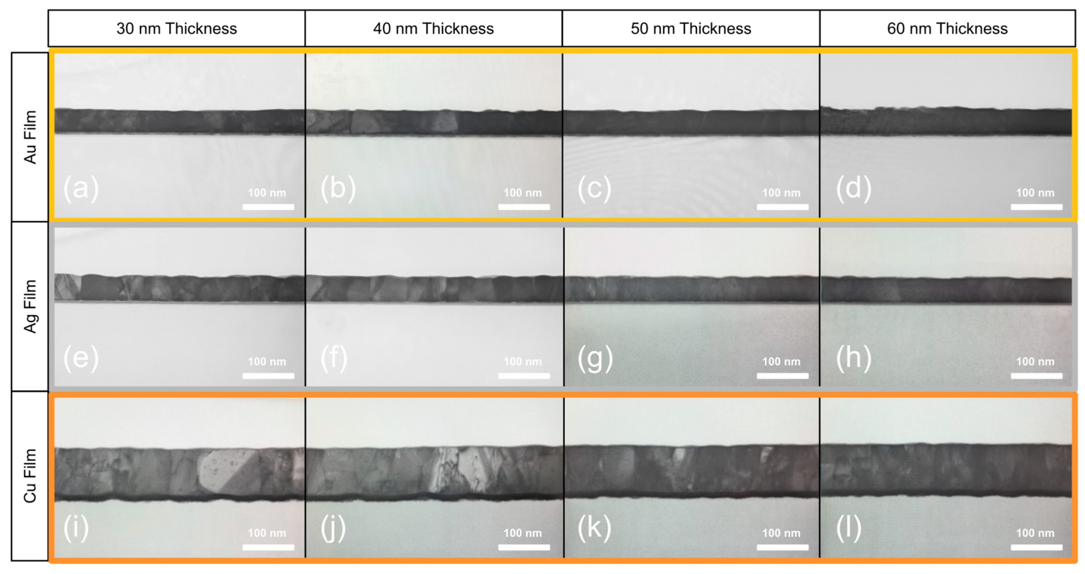
Experimental phase #4 was used to obtain target thickness values needed to achieve electron transparency for various thin-film metals, Cu, Au, and Ag. Each sample type was thinned and 30 kV STEM-imaged with TEM lamella window thicknesses of 30 nm, 40 nm, 50 nm, and 60 nm. This phase was used to show the utility of the technique by demonstrating that we can obtain a targeted thickness measurement that can be used to guide and optimize thin-film lamella thinning in a production environment. By obtaining the maximum thickness needed for specific materials, one prevents rework on the TEM lamella, which occurs when a sample is not thin enough.
2.2. Summary of Current Process
TEM lamella is typically fabricated using conservative beam values during the final thinning process in both the FIB and SEM to prevent material shrinkage and lamella warping. This typically means that the final thinning FIB operates at 2–5 kV for TEM prep and the SEM uses a 2 kV beam while final thinning in SE mode or at 10–20 kV for STEM transparency monitoring, with both methods using a low electron current of 100 pA. There is limited overlap between these SEM imaging methods, which means that an operator would most likely not perform 20 kV SE mode or 2 kV STEM mode analysis since a SE image taken at 20 kV would not provide surface information and a STEM image taken at 2 kV would not provide electron transparency. Our work has evaluated this middle ground using a sweep of voltages ranging from 2–15 kV, and we have found that we can directly monitor the thickness of a lamella in real time while at the thinning-stage position using SE mode in the SEM.
2.3. Modified Thinning Process
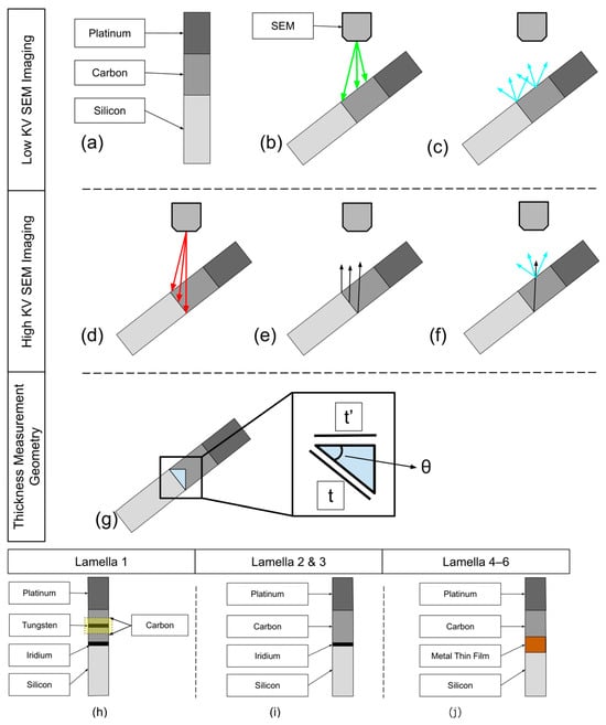
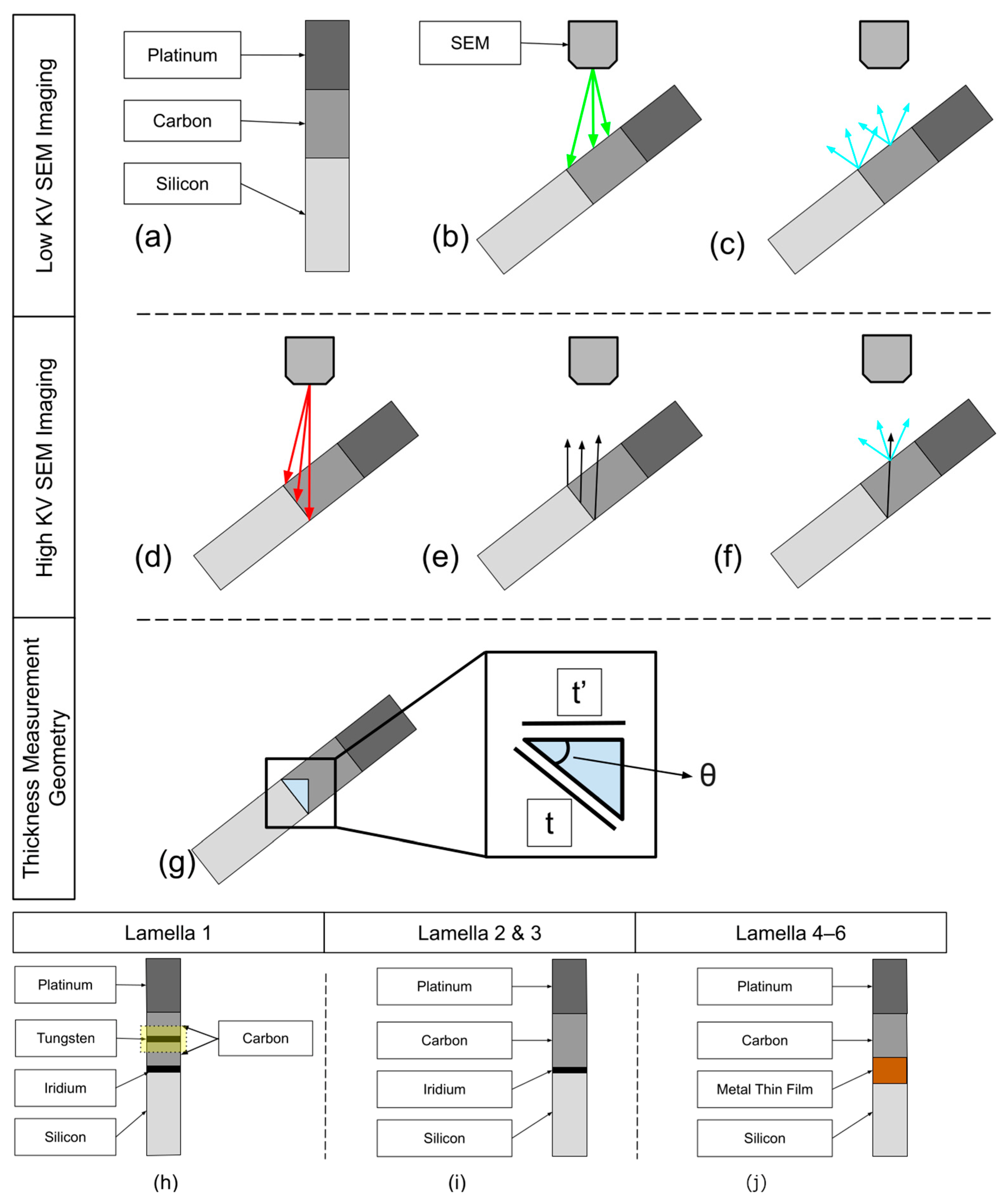
Figure 1 introduces low-energy secondary electron imaging and high-energy secondary electron imaging. In Figure 1, (a) we identify the basic materials in a lamella, platinum-protective FIB cap, electron beam-deposited carbon, and silicon substrate. (b, c) illustrate SEM imaging at low kV; the primary beam generates SEs and forms an image of the surface. (d–f) illustrate SEM imaging (d) at higher kV with the primary beam penetrating deeper into the lamella, (e) creating backscattered electrons, which are converted (f) into secondary electrons on the surface of the lamella, and an SE image is captured. The high-energy SE image contains information from both the front surface and the back lamella surface using a convolution of SEs. Figure 1g illustrates the relationship used to convert the observed thickness to the real lamella thickness. Since the stage is tilted between 48–56°, a tilt correction is applied. This range of tilts represents the typical lamella thinning tilts. We find t’ = t × cos(stage tilt), where t is the real thickness and t’ is the apparent thickness while the stage is tilted. We can measure t’ and obtain t for real-time thickness monitoring.
Figure 1.
The figure illustrates the lamella film stack and the SE/BSE imaging process. The figure also shows the lamella composition for each phase. (a) shows protective platinum cap, carbon film, and silicon substrate. (b) shows the primary beam incident on lamella. (c) shows the SE captured for image formation. (d–f) shows the imaging process with high-energy SEM. (d) A high-energy SEM beam is incident on the sample with a large penetration depth. (e) BSE are generated from deep inside the sample. (f) BSE are converted into SE at the surface of the lamella and used to generate the image. (g) shows the relationship between the observed thickness t’ and the real thickness t, t’ = t × cos(θ). Theta θ is 52° at the neutral mill position. (h) Lamella 1 was composed of a platinum cap, tungsten layer, iridium layer, silicon substrate, and two carbon layers surrounding the tungsten layer. (i) Lamella 2–3 were composed of a platinum cap, carbon layer, iridium layer, and silicon substrate. (j) Lamella 4–6 were composed of a platinum cap, carbon layer, thin-film metal, and substrate (silicon or SiO2).
Three lamellae were fabricated for phase #1–3, and three lamellae were fabricated for phase #4. Figure 1h–j shows the material composition of all six lamellae used in our work.
Experimental phase #1: Lamella #1 was used to demonstrate thickness monitoring and to identify optimal SEM image conditions used for thickness monitoring. The composition of lamella #1 is shown in Figure 1h. The sample was a silicon, iridium, carbon, tungsten, carbon, and platinum stack. Lamella #1 was used to evaluate the feasibility of creating a thickness monitoring layer that was independent of sample composition. In this configuration, the carbon, tungsten, and carbon stack represents our engineered multi-layered structure that allows thickness monitoring independent of the sample. The carbon layers are electron-transparent at high kV and allow direct imaging of the tungsten and iridium thickness. Both the embedded tungsten layer (highlighted in yellow in Figure 1h) and the surface iridium layer in Figure 1h were used to gauge sample thickness. A note on the engineered structure: by embedding the tungsten layer between two carbon layers above a device structure, we create a solution that can be implemented in an automated workflow where the image recognition program is tasked with identifying a single measurement line separated in position from device structures, reducing events of feature misidentification.
Experimental phase #2: Lamella #2 was used to demonstrate thickness targeting and was a platinum, carbon, iridium, and silicon stack, as shown in Figure 1j. The iridium layer acted as the measurement feature.
Experimental phase #3: Lamella #3 was used to demonstrate repeatability of the final thickness monitoring process and used the same stack as lamella #3, as shown in Figure 1j.
Experimental phase #4: Three lamellae were fabricated, each with a unique thin-film metal deposited onto a substrate, silicon or SiO2. A thick electron-beam-deposited carbon layer was fabricated onto the metal, and a FIB-deposited cap was applied above this. This configuration is shown in Figure 1j.
2.4. Sample Preparation: Process
A blanket 100-silicon wafer (Ted Pella Part Number 21610-510, Redding, CA, USA) was used as the sample substrate for this work for lamellae 1–3. A Quorum 150 sputter coater (Quorum Technologies, East Sussex, UK) was used to apply 10 s of iridium, approximately 5-nanometer-thick coating. This metal layer makes interface identification easier to perform. For lamellae 4–6, a 50-nanometer-thick gold-coated microscope slide was purchased from (Electron Microscopy Sciences, Morgantown, PA, USA), SKU 71892-05; a 50-nanometer-thick silver-coated microscope slide was purchased from Electron Microscopy Sciences, SKU 71892-30; and a 100-nanometer-thick Cu wafer with 10 nm tantalum barrier was provided by (Lam Research, Tualatin, OR, USA).
2.5. TEM Prep Tool
A Thermo Scientific 5FX dual-beam (Thermo Fisher Scientific, Hillsboro, OR, USA) with in situ easy-lift, multi-chemical gas-injection system (GIS), and in situ 30 kV-STEM capability was used to fabricate and characterize the TEM samples.
2.6. TEM Preparation: Process
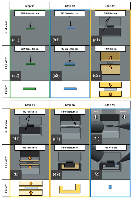
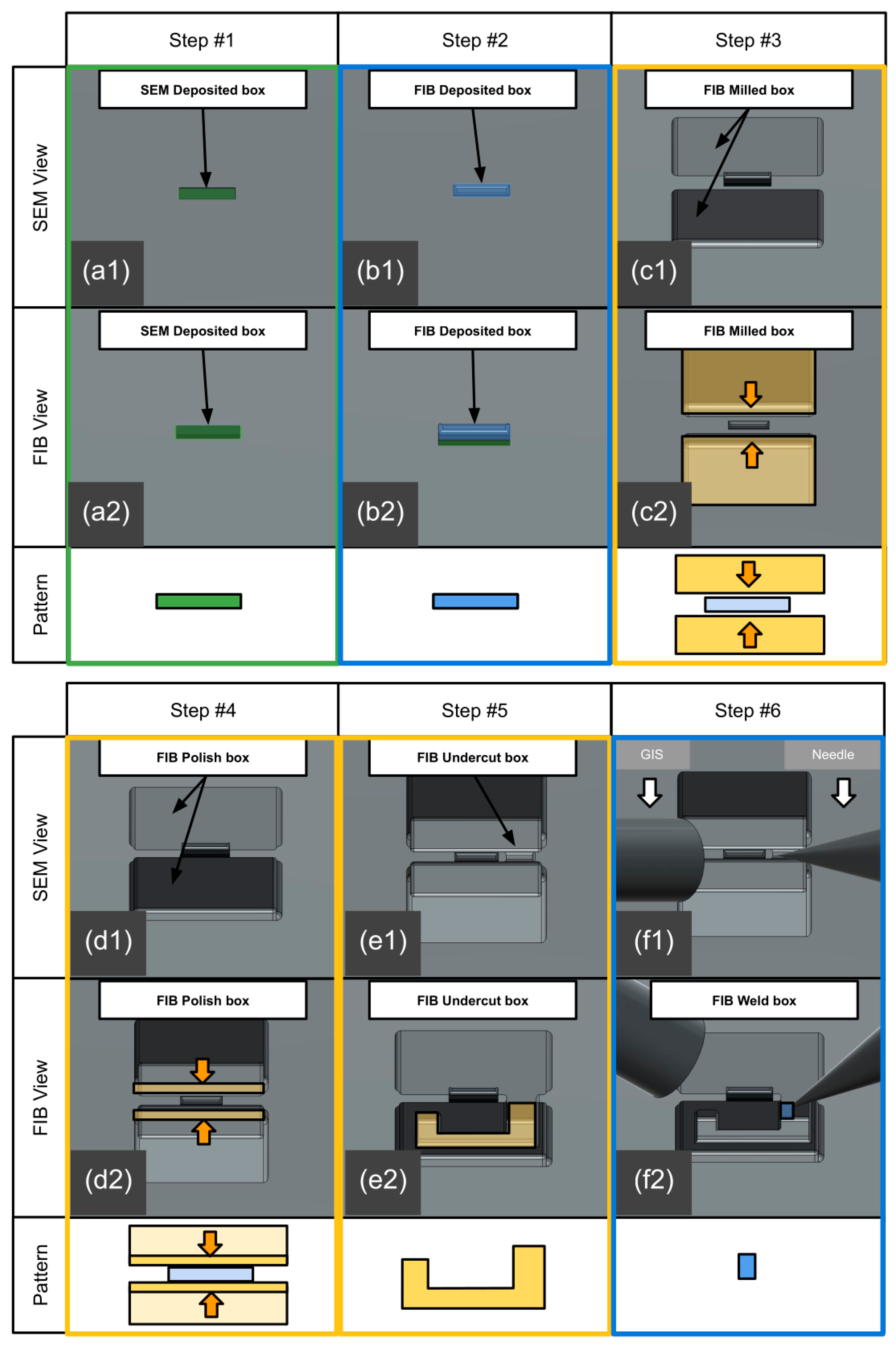
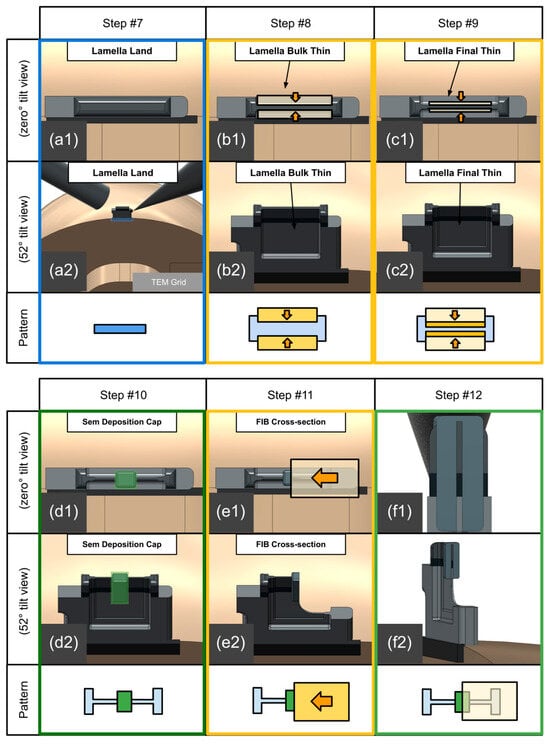
The bulk prep procedure for TEM prep is well described elsewhere [7]. We list the steps to create a lamella and move it to the TEM grid for final thinning. Figure 2 and Figure 3 show each step of the TEM prep process.
Figure 2.
Figure illustrates the TEM lamella preparation process and the lamella lift-out process. Step #1 shows the electron beam deposition process. (a1) illustrates SEM deposition from SEM fov. (a2) illustrates SEM deposition from FIB fov. Step #2 shows the FIB deposition process. (b1) illustrates FIB deposition from SEM fov. (b2) illustrates FIB deposition from FIB fov. Step #3 shows the FIB bulk mill #1 process. (c1) illustrates FIB mill from SEM fov. (c2) illustrates FIB mill from FIB fov. Step #4 shows the bulk mill #2 process to fine-mill the lamella surface. (d1) illustrates FIB polish mill from SEM fov. (d2) illustrates FIB polish mill from FIB fov. Step #5 shows the undercut process needed to lift out the lamella. (e1) illustrates FIB undercut mill from SEM fov. (e2) illustrates FIB undercut mill from FIB fov. Step #6 shows the lamella extraction process to lift out the lamella. (f1) illustrates lamella lift-out from SEM fov. (f2) illustrates lamella lift-out from FIB fov. The process pattern’s geometry is shown below the SEM and FIB images for each step. Note on pattern colors: Green is SEM deposition, blue is FIB deposition, and orange is FIB mill. Faded colors are used to show previous steps.
Figure 3.
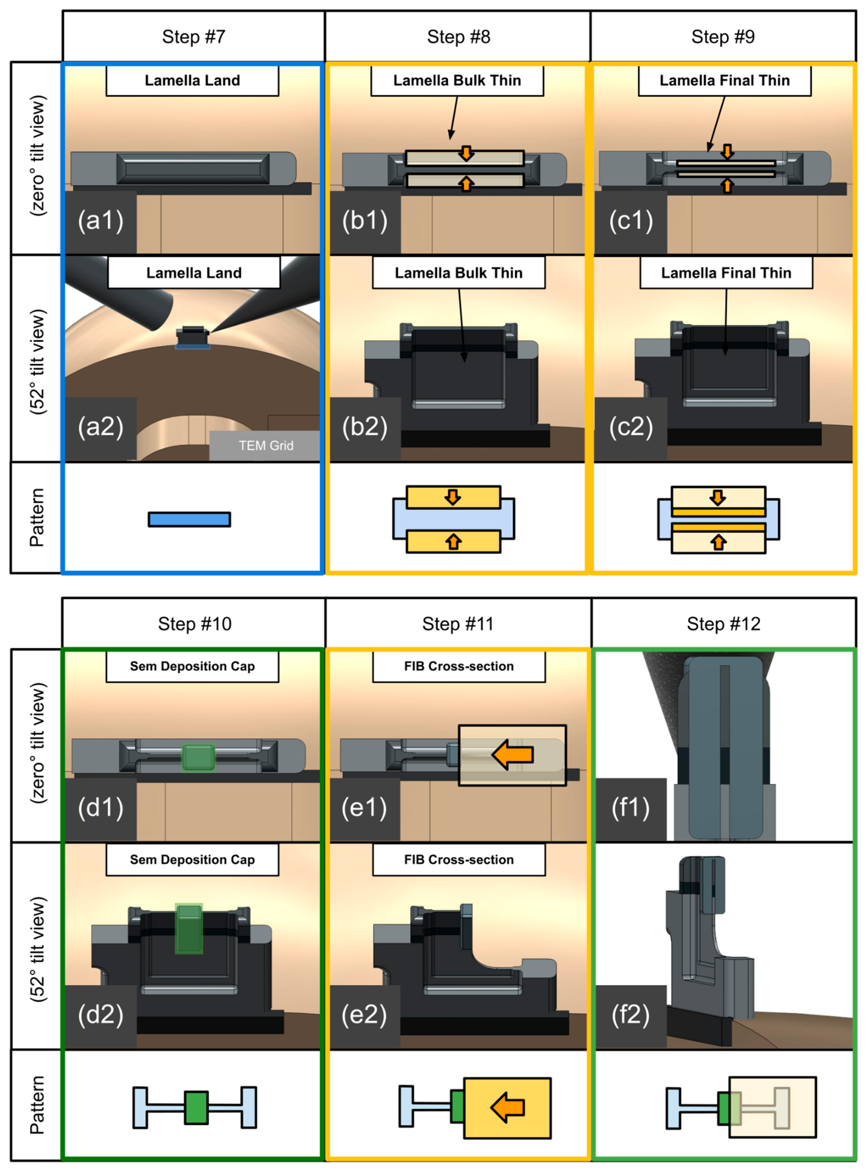
Figure illustrates the lamella welding to the TEM grid and the thinning processes. The post-cross-section process is also shown. Step #7 shows the landing on the TEM grid process. (a1) illustrates lamella landing on the grid from SEM fov. (a2) illustrates lamella landing on the grid from FIB fov. Step #8 shows the bulk-milling of the lamella. (b1) illustrates bulk milling from FIB fov. (b2) illustrates bulk milling from SEM fov. Step #9 shows the low kV final thinning. (c1) illustrates low kV FIB milling from FIB fov. (c2) illustrates low kV FIB milling from SEM fov. Step #10–12 show the cross-sectioning process. (d1) illustrates SEM deposition of platinum from FIB fov. (d2) illustrates SEM deposition of platinum from SEM fov. (e1) illustrates FIB cross-section milling from FIB fov. (e2) illustrates FIB cross-section milling from SEM fov (f2) shows an angular perspective to illustrate geometry. (f1) shows the cross-sectional view of the lamella stack. Note on pattern colors: Green is SEM deposition, blue is FIB deposition, and orange is FIB mill. Faded colors are used to show previous steps.
Bulk Prep:
- Figure 2 Step #1 (a1, a2): SEM deposition was used to deposit carbon using an in situ gas-injection system (GIS). The stage was tilted to 0° during this process. The SEM was set to 1 kV, 6.4 nA, using ultra high resolution (UHR) mode, through lens detector (TLD) with secondary electron biasing. The SEM Crossover was verified prior to deposition. A deposition time of 30 s per 1 µm2 was used. The carbon application type was used with a rectangular pattern.
- a.
- For lamella #1, after the first carbon layer was deposited, a 15 s deposition of tungsten was performed using the same beam conditions. A tungsten application type was used with a rectangular pattern. Then a second carbon layer was deposited using the same process as the first carbon deposition. For experimental phase #2–4, only a single carbon layer was fabricated.
- Figure 2 Step #2 (b1, b2): The FIB was used to deposit a platinum cap using in situ GIS. The stage was tilted to 52° during this process. The FIB was set to 8 kV, 0.35 nA, using an internal chamber electronics (ICE) detector, with SE biasing. The platinum application type was used with a rectangular pattern. The target thickness was approximately 800 nm.
- Figure 2 Step #3 (c1, c2) bulk mill #1: The sample was bulk milled using a 30 kV, 9.9 nA FIB beam. A silicon application type was used with two regular cross-section patterns. The stage was tilted to 52° during this process. The target depth of the mill was approximately 7 µm.
- Figure 2 Step #4 (d1, d1) bulk mill #2: The sample was milled using a 30 kV, 2.4 nA FIB beam. A silicon application type was used with two cleaning cross-section patterns. The stage was tilted to 52° during this process. The target depth was 6 µm.
- Figure 2 Step #5 (e1, e2) FIB undercut: The sample was undercut-milled using a 30 kV, 2.4 nA FIB beam. A silicon application type was used with a polygon pattern to create a J-cut. The stage was tilted to 0° during this process. Milling was performed until the SEM could observe that the J-cut fully milled all the way through the lamella.
- Figure 2 Step #6 (f1, f2), the lamella lift-out process: The sample was placed at beam coincidence. The stage was tilted to 0° during this process. A sharpened easy-lift needle was inserted, lowered into the trench, and welded to the TEM lamella using the FIB at 30 kV, 90 pA using Carbon Multi-Chem deposition. The weld took approximately 30 s. The lamella was then cut free from the bulk using 0.79 nA in the FIB using a line mill. The line mill took approximately 20 s. The lamella was raised 100 µm above the sample, and the easy-lift needle was retracted. The Multi-Chem GIS was also retracted.
- Figure 3 Step #7 (a1, a2), weld to grid: The TEM grid was placed at beam coincidence. The stage was tilted to 0° during this process. The easy-lift needle with the lamella was reinserted and lowered to the TEM grid and welded using 30 kV, 0.23 nA with Carbon Multi-Chem deposition. The pattern geometry is shown below the “lamella land on grid” step in Figure 3. Deposition time was approximately 60 s. The needle was cut free using 30 kV, 0.79 nA in the FIB and retracted. The Multi-Chem GIS was also retracted.
- Figure 3 Step#8 (b1, b2), frontside thinning #1: The TEM grid was tilted to 52° to be normal to the FIB, and the edges of the lamella were FIB-milled to be cleaned up with two small cleaning cross-section mills. The mill was performed with a 30 kV, 0.44 nA FIB beam. The patterns are shown relative to the FIB, and milling was performed normal to the TEM grid.
- Figure 3 Step#9 (c1, c2), frontside thinning #2: An 8 kV 11 pA FIB was used to polish the front of the lamella. A cleaning cross-section pattern was used. The mill depth was tuned to mill at least 1 µm below feature level, z = 3.5 µm, vol/dose = 0.87 µm3/nC. An alpha flip tilt of +2° was applied to the stage prior to milling, giving a sum tilt of 54°. A 2 kV 100 pA SEM was used to verify the surface was milled with the correct position and depth. This was performed in UHR-SE mode.
- Figure 3 Step #9 (d1, d2), backside thinning #1: An 8 kV 11 pA FIB was used to polish the back of both lamellae. A cleaning cross-section pattern was used. The mill depth was tuned to mill at least 1 µm below feature level, z = 3.5 µm, vol/dose = 0.87 µm3/nC. A tilt of −2° was applied to the stage prior to milling, giving a total tilt of 50°. The SEM was set to 10 kV, 0.4 nA, UHR mode using SE. For experiment phase #1, the lamella was thinned down to a final thickness of approximately 40 nm by measuring the lamella thickness using a tilt-corrected surface measurement. For experiment phase #2, each of the five windows was thinned down to target thicknesses using tilt-corrected surface measurements. Each of the five windows was targeted to different, discrete thicknesses. For experiment phase #3, each of the 10 windows was thinned down to the same target thickness using tilt-corrected surface measurements. The first lamella window was thinned down to 32 nm; therefore, all of the other nine windows were targeted for 32 nm as well. For experiment phase #4, for the three material types, four windows were fabricated into each lamella, and each was thinned down until a target thickness was achieved. The target thicknesses were 30 nm, 40 nm, 50 nm, and 60 nm.
STEM Imaging:
For experiment phase #1, STEM imaging was performed at 4.15 mm working distance (WD) with a stage alpha flip tilt of 52°. The SEM was set to 15 kV, 400 pA, UHR mode. Bright-field and dark-field images were acquired. By imaging at 52°, we obtain the perspective to measure sample thickness.
For experiment phase #4, STEM imaging was performed in in-lens mode with a 1.9 mm WD with a stage alpha flip tilt of 90°. The SEM was set to 30 kV, 25 pA, UHR mode. Bright-field images were acquired. In-lens mode is a newer feature on the Helios 5FX that allows higher-resolution STEM imaging (3 Å) by having a lower lens, fully immersing the lamella in a magnetic field.
Lamella cross-sectioning process:
Figure 3 Step #10 (d1, d2): The SEM was used to deposit platinum on both sides of the lamella. The front of the lamella was coated with electron-deposited platinum using a 1 kV, 0.8 nA beam. The deposition time was approximately 30 secs using a pattern size to cover the center of the thinned window, approximately 1.5 µm × 1.5 µm. The lamella was then flipped 180° using a beta flip rotation, and the backside of the lamella was coated using the same process.
Figure 3 Step#11 (e1, e2): The FIB was used to cross-section the lamella using a 30 kV, 90 pA beam with a cleaning cross-section pattern type. The lamella was rotated to an absolute 90 degrees in the beta axis and tilted to 52° in the alpha flip tilt axis.
Figure 3 Step#12 (f1, f2): The SEM was used to image the cross section using a 5 kV, 100 pA beam, UHR mode with TLD-SE. The cross-sectioned SEM images were acquired at a stage tilt of 52°.
2.7. Measurements and Error Estimation
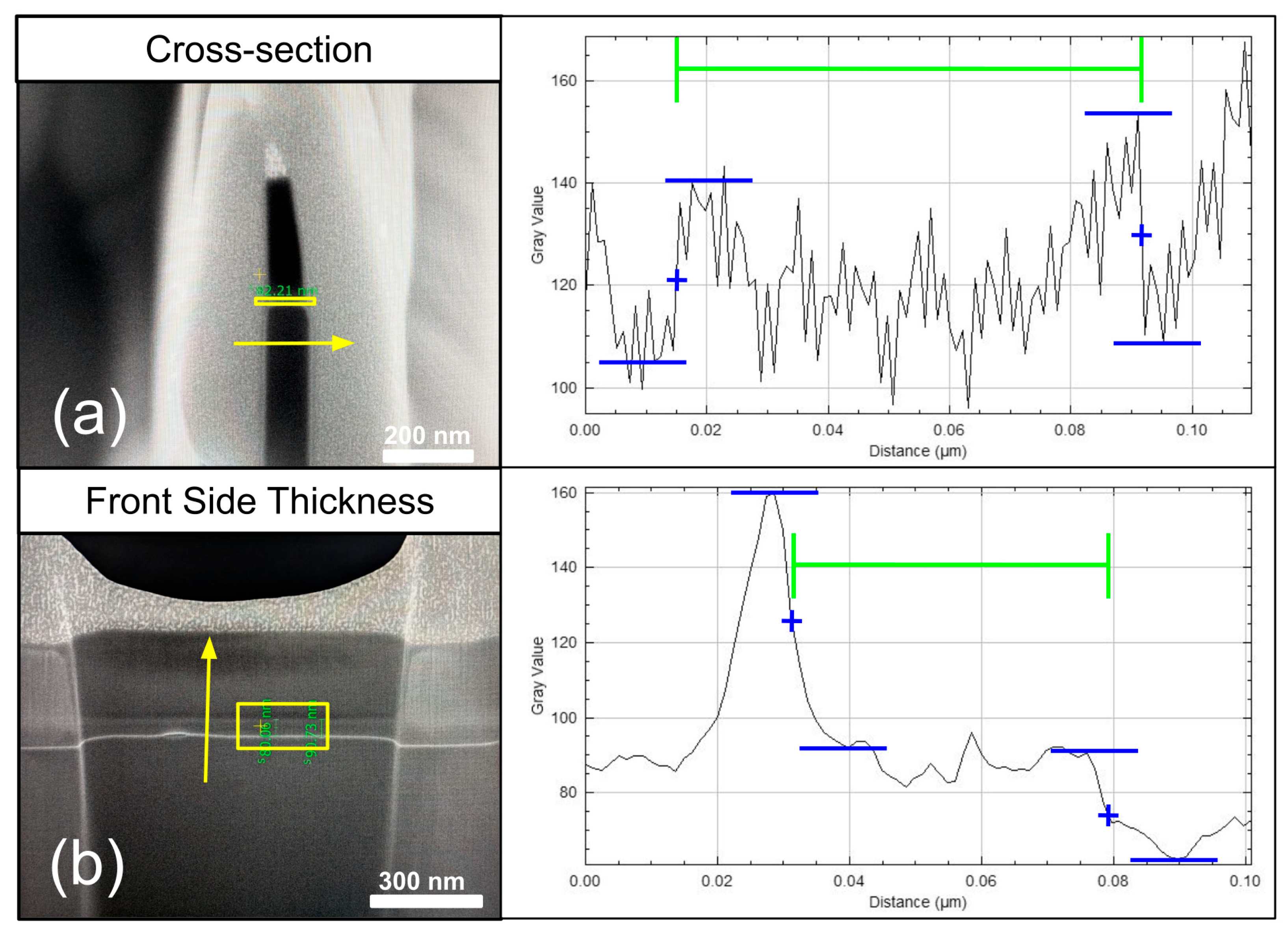
Initial measurements during the experiment were performed using a single-line measurement in the SEM feature with tilt correction applied. Post-processing measurements for evaluating the technique were performed using a box average using Imagej software (version 1.54d). For the frontside measurements, the box size was approximately 100 × 200 nm2, with averaging being performed along the longer direction, meaning we are performing approximately 200 line measurements in each box. Cross-section images used a box measurement with a 10-nanometer-tall line average in the vertical axis and a 50–150 nm line in the horizontal axis. The vertical axis height was limited due to layer height. The cross-section measurements averaged over 10 nm, giving approximately 10 line measurements. Figure A1 in Appendix A.2 illustrates the post-process measurement procedure on a frontside lamella SEM image and cross-section lamella SEM image.
To calculate the standard deviation for measurements of SEM images shown in Figure A3, we find the difference between the frontside measurement and the cross-section measurement and then calculate the standard deviation using the standard deviation function in Excel and apply it to the difference values. This yields a standard deviation of 1.9 nm.
The error estimates for the SEM measurements are estimated to be limited by the electron spot size, which from the tool manufacturer is approximately 1–3 nm. This value is dependent on the interaction volume and therefore material-dependent. We will use a 3 nm value for our error estimates. The measurement calibration accuracy is generally specified at 1%. The error in the measurement from tilt error is estimated to be (+/−) 0.1 degrees. The tilt axis is a closed loop, and little error is observed. To estimate the error in a 30-nanometer-wide lamella measurement, we use the equation for the apparent thickness and the actual thickness and estimate the errors. Error contributed from tilt positioning: dt’ = t × cos(52.1) − t × cos(51.9); with t being 30 nm, we find dt’ = 0.22 nm.
Measurement error from stage drift: The specification for stage drift is approximately 5 nm per minute. The total image acquisition time is 10 s when scanning at 1024 × 884 pixels with a line integrate of 2 and dwell time of 3 μs. This can result in a compression or expansion of the image. The error estimated from stage drift is 5 (1 nm/60 s)*10 s = 0.83 nm. This gives an error of (+/−) 0.83 nm.
Our largest source of error is measurement error in the SEM measurements and stage drift. We estimate the SEM contribution to be half of the uncertainty in the SEM spot size. This gives an error in SEM measurements of (+/−) 1.5 nm. We add the stage drift to the SEM image uncertainty and get a total estimated error of (+/−) 2.3 nm.
3. Results
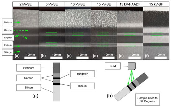
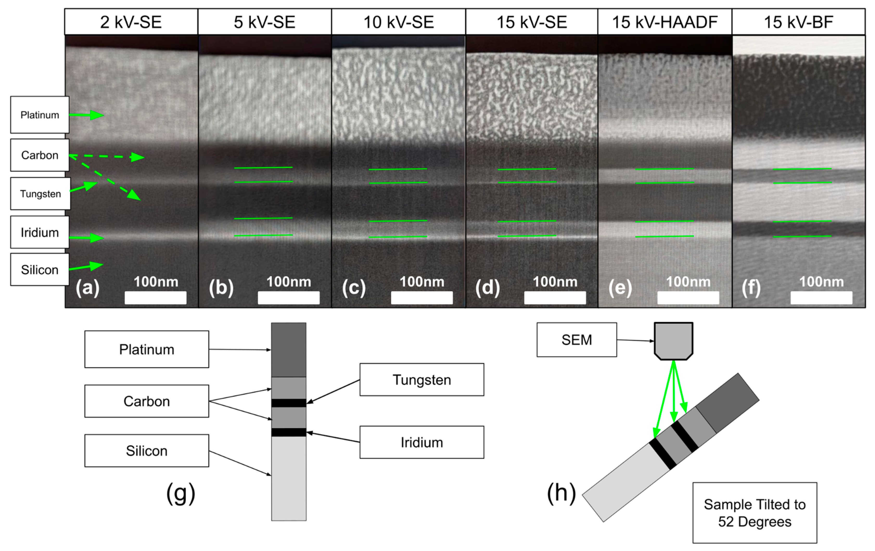
Lamella #1 was imaged with the SEM using 2–15 kV (2, 5, 10, and 15 kV), 0.4 nA using UHR mode to explore imaging conditions and detector configurations, as shown in Figure 4. Imaging was performed at the neutral mill position, 52°. (a) Imaging at 2 kV using SE only shows the front surface of the lamella with little information from within the lamella. No thickness measurement could be made. (b) SEM imaging at 5 kV in SE mode shows a blurry edge starting to appear from the features within the lamella. A rough thickness measurement was made. (c) Imaging at 10 kV and (d) 15 kV using SE shows the back edge of the lamella is well defined, and measurements are easily made. Imaging at 15 kV, using a STEM mode, both (f) bright field (BF) and (e) high angular annular dark field (HAADF) were acquired, and thickness measurements were made. These measurement results were summarized in Table 1. Figure 4g illustrates the material composition of the lamella, and (h) illustrates the sample tilt relative to the SEM.
Figure 4.
Demonstrates the visibility of the layers as the acceleration voltage is increased. (a) 2 kV SEM SE image, (b) 5 kV SEM SE image, (c) 10 kV SEM SE image, (d) 15 kV SEM SE image, (e) 15 kV STEM HAADF image, and (f) 15 kV STEM bright-field image. Green horizontal lines indicate measured regions. (g) shows the lamella composition. (h) shows the lamella tilt relative to the SEM.
Table 1.
Summary of layer measurements obtained with various beam conditions for phase #1.
After frontside thickness measurements were made, a cross section was made of the lamella, and thickness measurements were made for the two layers within the lamella (surface iridium layer and embedded W layer within the carbon layers). All frontside thickness measurements were within 5 nm of the cross-sectioned thickness values.
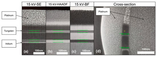
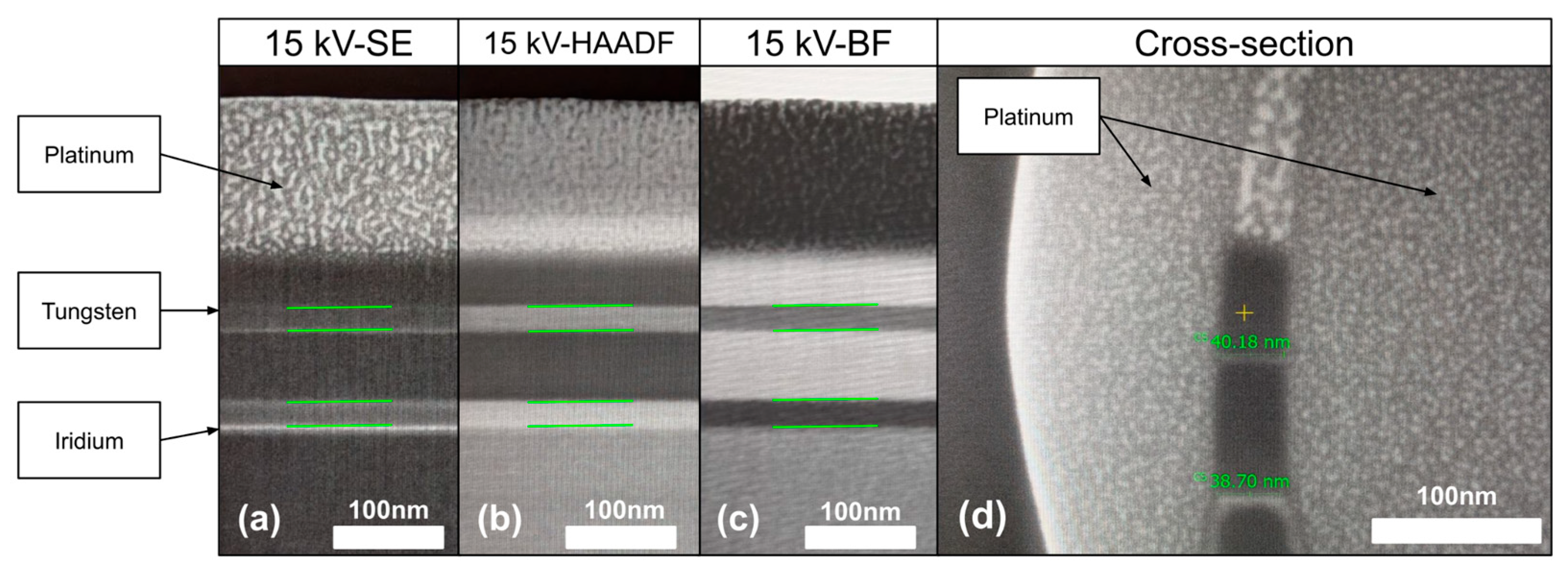
Figure 5 allows for direct comparison of the 15 kV SE SEM images and the STEM images. Comparing the SE 15 kV image (a) to the 15 kV STEM (b, c) images, one notices that the thickness measurement of the iridium layer in the HAADF image has a 3 nm discrepancy. This is caused by the layer thickness being included in the STEM thickness measurements, whereas the SE thickness measurement is able to delineate the layer thickness and the lamella thickness. For the embedded W layer, which is thinner than the iridium layer, the 15 kV, STEM images are closer to the cross-sectioned thicknesses. The 5 kV SEM images had the most deviation between frontside measurements and cross-section measurements, with measurements varying 4 nm and 10.7 nm for the iridium and tungsten layers, respectively.
Figure 5.
Comparison of the 15 kV SE SEM image and the STEM BF, DF images. The cross-section SE SEM image is for reference. (a) 15 kV SE image, (b) 15 kV HAADF STEM image, (c) 15 kV BF STEM image, and (d) cross-section SE image of lamella. Green horizontal lines indicate measured regions.
Each window of lamella #2 was imaged at the neutral mill position (52° alpha flip), with the SEM at 10 kV, 0.4 nA using UHR SE mode, as shown in Figure A2 in Appendix A.2. The thicknesses are summarized in Table A1 in Appendix A.2. For each window, a target thickness was used as a stopping point, shown in the right column of Figure A2. Once the lamella thickness was equal to or less than the target, the thinning was stopped. A measurement of the final thickness and the cross-section thickness was made. Cross-section results are shown in the left column of Figure A2. Cross-sectioned SEM images were acquired with the SEM using 5 kV, 100 pA using UHR SE mode. For the 28.5 nm target window, the cross section was 26.8 nm. For the 45 nm target window, the cross section was 47 nm. For the 60 nm target window, the cross section was 59.7 nm. For the 77.4 nm target window, the cross section was 76.9 nm. For the 112 nm target window, the cross section was 99.4 nm. For all five windows, there is less than a 13 nm difference between measured target thickness and cross-section thicknesses. Excluding the 99 nm lamella, all of the other four lamella had less than 2 nm of difference. It is observed that as the lamella becomes thicker, the comparison between measured thicknesses and cross-sectioned thickness becomes less reliable. This is attributed to the poorer resolution of the back edge of the lamella as the lamella thickness is increased.
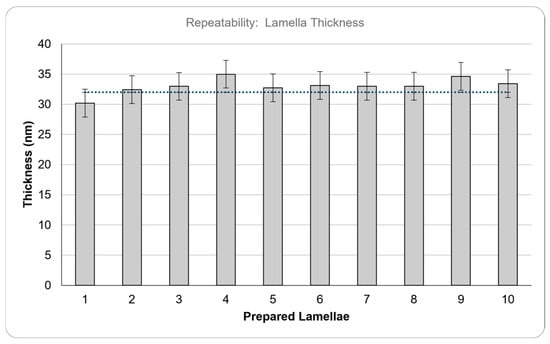
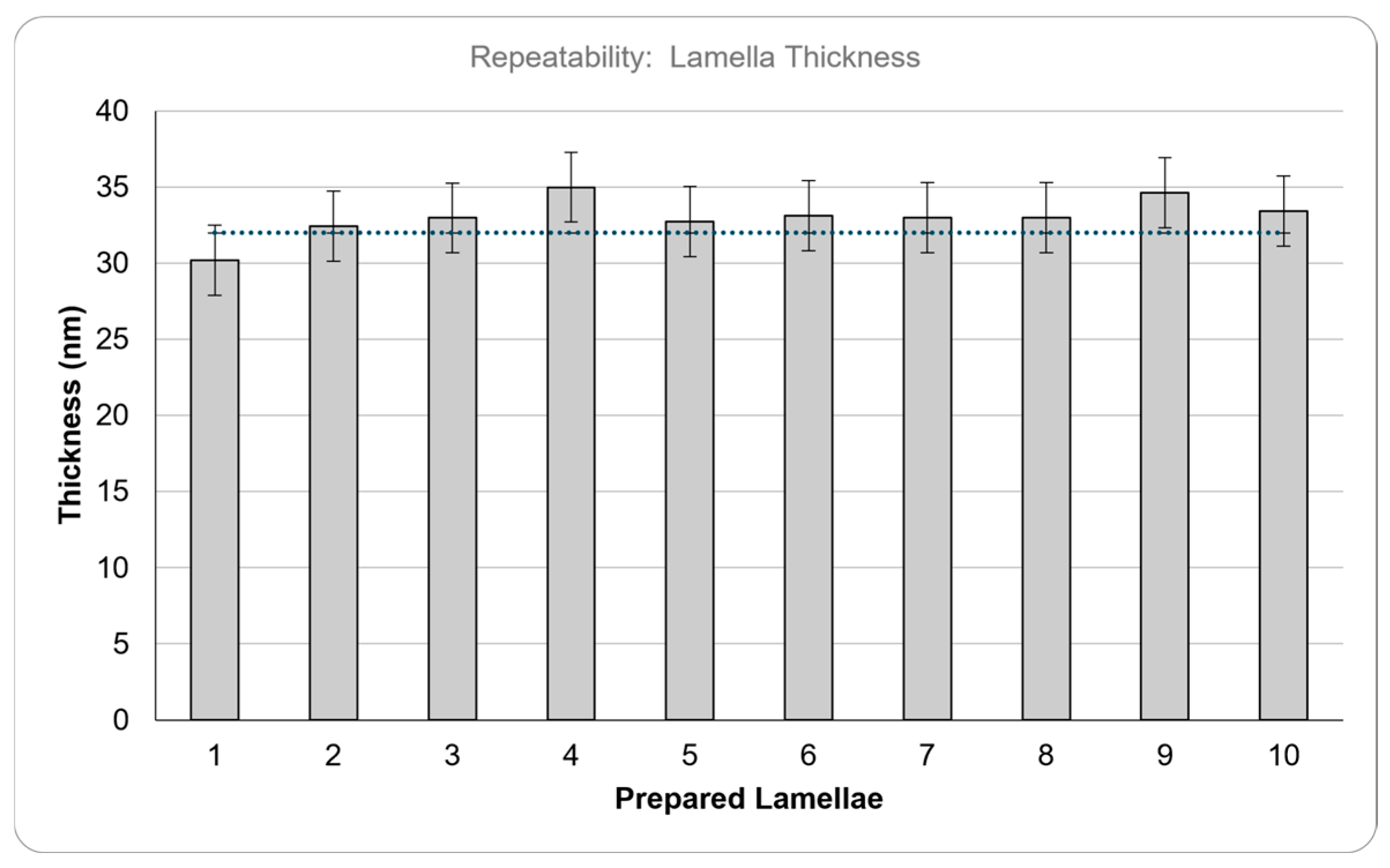
Results from phase #3 demonstrate the effectiveness of the technique for obtaining repeatable lamella thicknesses. SEM images are shown in Figure A3 in Appendix A.2. The minimum and maximum measured thicknesses were between 31.4 nm and 36.5 nm. The minimum and maximum thickness measured in the cross sections were between 30.2 nm and 34.7 nm. For both sets of measurements, there was approximately a 5 nm difference between maximum and minimum. This is comparable to the estimated error of the measurement. Lamella window thicknesses are plotted in Figure 6 and summarized in Table A2, shown in Appendix A.2. The error bars shown in Figure 6 are (+/−) 2.3 nm. A horizontal target line of 32 nm is shown.
Figure 6.
Plot shows cross-section lamella thickness plotted with a target line of 32 nm. Results from phase #3. The error bar is (+/−) 2.3 nm.
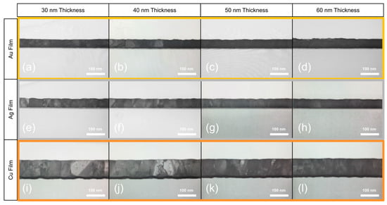
Results from phase #4 offer insight into the processing requirements to obtain electron transparency in various thin-film metals. It was qualitatively found that the electron transparency is proportional to crystal grain size. As the width of the lamella gets thinned down to a single crystal width, electron transparency and contrast between adjacent crystals increases. In Figure 7a–d, we observed that the Au thin film has the smallest grains and only exhibits grain contrast for large crystals around 40 nm thickness. Even the 30-nanometer-thick Au lamella does not show grain contrast as one would need for grain measurements. In Figure 7e–h, we observed that the Ag thin film has a smaller grain than our Cu sample and only starts to exhibit notable grain contrast around 40 nm thickness. The Cu thin film, shown in Figure 7i–l, has the largest crystal structure and has good grain contrast starting at 50 nm thick and improves as the sample is further thinned.
Figure 7.
STEM images for Au, Ag, and Cu thin-film samples with various thicknesses for phase #4. (a) Au thin film 30 nm thick lamellae; (b) Au thin film 40 nm thick lamellae; (c) Au thin film 50 nm thick lamellae; (d) Au thin film 60 nm thick lamellae; (e) Ag thin film 30 nm thick lamellae; (f) Ag thin film 40 nm thick lamellae; (g) Ag thin film 50 nm thick lamellae; (h) Ag thin film 60 nm thick lamellae; (i) Cu thin film 30 nm thick lamellae; (j) Cu thin film 40 nm thick lamellae; (k) Cu thin film 50 nm thick lamellae; (l) Cu thin film 60 nm thick lamellae; Color frame added to highlight the material type in each row. Please note, each window was thinned into a different section of the lamella, therefore different grains are shown for each image.
4. Discussion
Phase #1 has demonstrated that direct lamella thickness measurement can be performed using the SE imaging mode with a moderate acceleration voltage. It was found that a SEM of 10–15 kV and a beam current of 0.4 nA can be used to SE image the lamella thickness. A comparison of SE and BF, DF STEM images was made. It was found that the SE images were able to separate the reference layer thickness and the sample thickness, whereas the STEM images were unable to make this delineation. It was found that as long as the reference layer was thin, all detectors were able to be within a few nanometers of the actual lamella thickness. A key benefit of using a SE SEM image technique is that it can be implemented in workflows that cannot support STEM detector usage, i.e., TEM sample prep using a bulk stage. This technique does not require specialized detectors or detector brightness and contrast calibration to perform the measurement. This simplicity is a step toward broader adoption.
In phase #1, we were able to demonstrate the fabrication and utilization of a multi-layered lamella thickness monitoring structure that is independent of the sample. The sample thickness measurements made at both measurement features (surface iridium layer and embedded tungsten layer) were found to be within a few nanometers and in good agreement. By creating an embedded reference layer of tungsten between electron-transparent carbon layers using electron beam deposition, this technique can be applied to many sample types and does not rely on the semiconductor device having a measurable feature. The utilization of a sample-independent measurement feature offers robustness to contrast changes that occur when the sample material is changed, since the measurement materials and measurement region are separate from the sample material.
The embedded tungsten layer is also a step toward an automated solution. In an automation workflow, a computer program can be used to implement a vertical double-edge finder to identify and monitor the top and bottom positions of this tungsten layer in the SEM and get a measurement of the current lamella thickness in real time. Offsetting the tungsten layer from the sample device using a carbon layer allows a simpler measurement to be performed in an automated manner, since device structure could interfere with lamella thickness measurements. This is one practical and affordable way that tool manufacturers could implement closed-loop lamella thickness control.
For phases #2 and #3, we demonstrated that our lamella measurement technique is both accurate and precise. Phase #2 demonstrated accuracy by fabricating five lamellae with targeted thicknesses of 28 nm, 45 nm, 60 nm, 80 nm, and 100 nm. The deviation between target thickness and cross-section thickness was 13 nm or less. Most of the variation in lamella thickness measurements was observed in the thicker lamellae due to the large interaction volume of the BSE mode. In the semiconductor industry, the ability to target discrete thicknesses allows each semiconductor device to be encapsulated within a lamella using a unique target thickness.
Phase #3 demonstrated precision by fabricating 10 STEM with a targeted thickness of 32 nm and a variance of approximately 1.9 nm. The ability of our technique to produce accurate and precise lamella is due to the simplicity of the technique, which is independent of the operator’s skill. The technique is simply performing direct tilt-corrected measurements on a SEM image, a skill that technicians can implement.
Phase #4 utilized our thinning workflow to evaluate the minimum thickness needed for electron transparency for various thin-film metals. This is a useful parameter in a production lab environment. The typical workflow in a production lab is to attempt thinning on a lamella and then possibly re-thin the lamella due to insufficient imaging resolution due to sample thickness. This workflow arises due to the artisan nature of TEM prep, which lacks a simple and direct measurement technique. By obtaining a direct measurement and a target lamella thickness, this rework is prevented. In phase #4, it was found that the minimum lamella thickness for thin-film metal samples is proportional to the grain size in the thin film. Rarely is the grain size of a sample known prior to TEM processing. We observed that lamella between 30–40 nm thickness exhibited sufficient grain contrast for all materials, but overall, a thinner lamella will produce improved grain analysis. The thickness measurement process is used to ensure that lamella processing needs to be only performed once when a target thickness parameter is known prior to processing.
Compared with other lamella thickness measurement techniques, we find that EELs are the most accurate with an estimated accuracy of 5–10%, with the accuracy highly dependent on the inelastic mean free path of the electron [34]. This value is generally provided in a database. The BSE intensity thickness measurement gives a relative error of 20% and generally performs poorly at low atomic weight materials [10]. The calibrated SE intensity thickness measurement technique is generally estimated to have a relative error of 20% and is stated to have poor performance due to detector variation [16]. EDX intensity-calibrated lamella thickness measurements are stated to be within 2.6% of EELs’ accuracy [28] and require dedicated hardware. The error observed in our technique was found to be dependent on sample thickness. Looking at the error found in phase #3 evaluating 32 nm target thicknesses, the average error between thickness measurements and cross-section measurements was found to be 3%, and a standard deviation for the error was 5.6%. Looking at the thicker lamellae, the error found in the 100-nanometer-thick lamella was 13%. This puts our technique comparable with BSE intensity and SE intensity thickness measurement techniques and not much worse than EELs and EDX thickness measurements.
Compared to EELs, we do not need to unload the TEM sample and transfer it to the TEM to measure the thickness. The need to re-thin the sample is avoided. In a production environment, this saves significant time and increases the efficiency of the lab. For calibrated EDX/BSE/SE thickness measurement processes, the workflow entails the need to calibrate and maintain calibration for all of the tools in the lab. This is expensive and a skilled process that is not scalable to a large production environment. Our process represents a small deviation from the standard TEM preparation process by requiring changing the SEM to UHR mode with different SEM settings (acceleration voltage and beam current).
Our process does not need special hardware to function, whereas an EELs system is estimated to cost $500,000 and an EDX costs approximately $50,000–100,000. These costs are per tool and represent a significant burden to lab-wide implementation. An EELs system requires the use of a TEM, which not all labs have readily available.
Our system is able to produce similar quality TEM samples as other thickness monitoring techniques. The reliability and repeatability of our technique is a significant upgrade to existing workflows. Material damage from the SEM imaging process is discussed in Appendix A.1, where the electron dose is calculated and compared with electron doses of other materials. Our imaging conditions are estimated to be toward the lower-dose region. In an abundance of caution, we recommend using a sacrificial region of the lamella window (1-micrometer-wide region) when working with delicate materials to prevent sample damage.
5. Conclusions
The workflow demonstrated here is a quantitative lamella fabrication process that can be broadly applied in the semiconductor industry. Our technique presented here is implementable with the standard electron microscope detectors and modes of operation. We have demonstrated that we can use a higher-energy SEM to directly measure and monitor TEM lamella thickness in real time, allowing control of lamella thickness. We demonstrated the fabrication of a sample-independent multi-layer structure that is used to measure lamella thickness. We used this technique to fabricate 10 TEM lamella with less than 2 nm standard deviation between frontside measurements and cross-section measurements. We utilized the technique to demonstrate the ability to target discrete lamella thicknesses. We have found that our technique has an accuracy that is dependent on lamella thickness with accuracy varying between 3–13%, with thinner lamella being more accurately characterized. We demonstrated that our technique can be used to identify ideal target lamella thicknesses for material-specific thin-film metals, allowing a repeatable production process to be developed. Overall, this technique is cheaper and comparable in performance to existing measurement processes, without the added need for extra hardware or the hassle of additional system calibrations. Some of the limitations that have prevented prior adoption of TEM lamella thickness monitoring processes, such as cost, ease of implementation, accuracy, and precision of technique, are resolved with our new process.
Funding
This research was funded by Lam Research and Portland State University.
Data Availability Statement
Data will be made available on request.
Acknowledgments
We would like to acknowledge Lam Research for their contribution of knowledge and microscope resources to perform this study. We would like to acknowledge Matt Hughes for his great insight into electron microscopy.
Conflicts of Interest
Author Monte Kozell was employed by the company Lam Research, Tualatin, USA. The author declares no conflicts of interest.
Abbreviations
The following abbreviations are used in this manuscript:
| BF | Bright Field |
| BSE | Backscatter Electron |
| EDS | Energy Dispersive Spectroscopy |
| EELS | Electron Energy Loss Spectroscopy |
| FIB | Focused Ion Beam |
| HAADF | High Angle Annular Dark Field |
| HAR | High Aspect Ratio |
| ICE | Internal Chamber Electron |
| SEM | Scanning Electron Microscopy |
| SE | Secondary Electron |
| STEM | Scanning Transmission Electron Microscopy |
| TEM | Transmission Electron Microscopy |
| TLD | Through Lens Detector |
| UHR | Ultra High Resolution |
| WD | Working Distance |
Appendix A
Appendix A.1. Estimating Electron Dose
Electron beam damage is a serious concern when performing any analysis on a semiconductor device. We estimate the electron dose that is accumulated during our imaging process and compare it to literature. Electron dose is defined as the number of electrons that have reached a sample’s surface for a given dwell time [35,36]
with d being electron dose, I being incident beam current, and S being irradiated surface area. We performed our imaging using a 0.4 nA beam, with 1024 × 884 pixels in the SEM image with a horizontal field of view of 847 nm, (1024/847) giving a pixel size and irradiated surface length per pixel of 1.2 nm or 12 Å.
We calculate the total charge accumulated in the sample for a given time:
I × t = 0.4 nA × 3.0 µs = 1.2 × 10⁻¹⁵ C
Converting charge to the number of electrons,
1.2 × 10⁻¹⁵ C × e−/1.602 × 10−19 C = 7490 electrons
Using Equation (A1), we find an electron dose for electrons per unit area:
d = 7490 electrons/(π × (12Å)2) = 16.6 electrons/Å2
In literature, we find a low electron dose used in STEM range from 5 electron/Å2 damaging some biological specimens, 100 electrons/Å2 being the dose used in cryo-EM for characterizing catalysts [37], and 100–5000 electrons/Å2 being a standard dose in HRTEM imaging [38]. Our dose is on the lower end of exposure for most materials. We exercise caution and recommend using a sacrificial region for thickness monitoring to prevent unnecessary exposure.
Appendix A.2
An example of the post-process-measurement procedure is shown. All other measurements shown in SEM images (green line measurements) are the initial experimental measurements used for performing the experiment. All reported measurement data used the more rigorous post-process-measurement procedure with box averaging. The figures below have both the endpoint image with measured thicknesses and the cross-sectional SEM images for thickness validation.
Figure A1.
The diagram demonstrates the measurement process using a box average. (a) shows the measurement region bounded by a yellow box for the cross-section image of the structure. (b) shows the measurement region bounded by a yellow box for the frontside thickness SEM image of the structure. The arrow indicates measurement direction. Box-averaged cross-section profiles with example measurements are shown in the right two panels. The upper panel corresponds to the cross-section measurement, and the lower right panel corresponds to the frontside thickness measurement. The blue line profiles represent the maximum and minimums at each edge, and the crosses represent the measurement edge. The green lines represent the measured distance.
Measurement Procedure:
Measurements were taken using a box averaged over 10 nm in cross-section images and over 200–250 nm in frontside measurements.
- Open Imagej software. Import image.
- Set Scale.
- a.
- The “Distance in Pixels” parameter uses the image dimension of 1024 pixels.
- b.
- Set “Known distance” using the SEM HFW.
- c.
- Set units nm.
- Draw a measurement rectangle on the SEM image.
- Select Plot Profile. This will plot the average box profile.
- Draw a box on the plot profile. For the left and right sides of the box, follow the procedure to define the edge.
- a.
- Find the maximum and minimum at an edge, as shown in Figure A1 (right panels), and define the measurement edge at the 50% midpoint vertically between them. Repeat this process for both sides of the feature.
- Select Measurement. This will create a table with the horizontal measurements listed.
- Apply tilt correction to frontside thickness measurements to obtain tilt-compensated measurement. (Multiply measured width by 1/cos(52°) for frontside measurements.) No tilt correction is applied to the cross-section images.
Figure A2.
SEM images of the cross-section lamella and of the final endpoint image for each lamella window in experiment phase #2. Measurements shown in Table A1. (a) Cross-section and (b) endpoint image for a 25 nm targeted lamella. (c) Cross-section and (d) endpoint image for a 44 nm targeted lamella. (e) Cross-section and (f) endpoint image for a 60 nm targeted lamella. (g) Cross-section and (h) endpoint image for a 80 nm targeted lamella. (i) Cross-section and (j) endpoint image for a 100 nm targeted lamella.
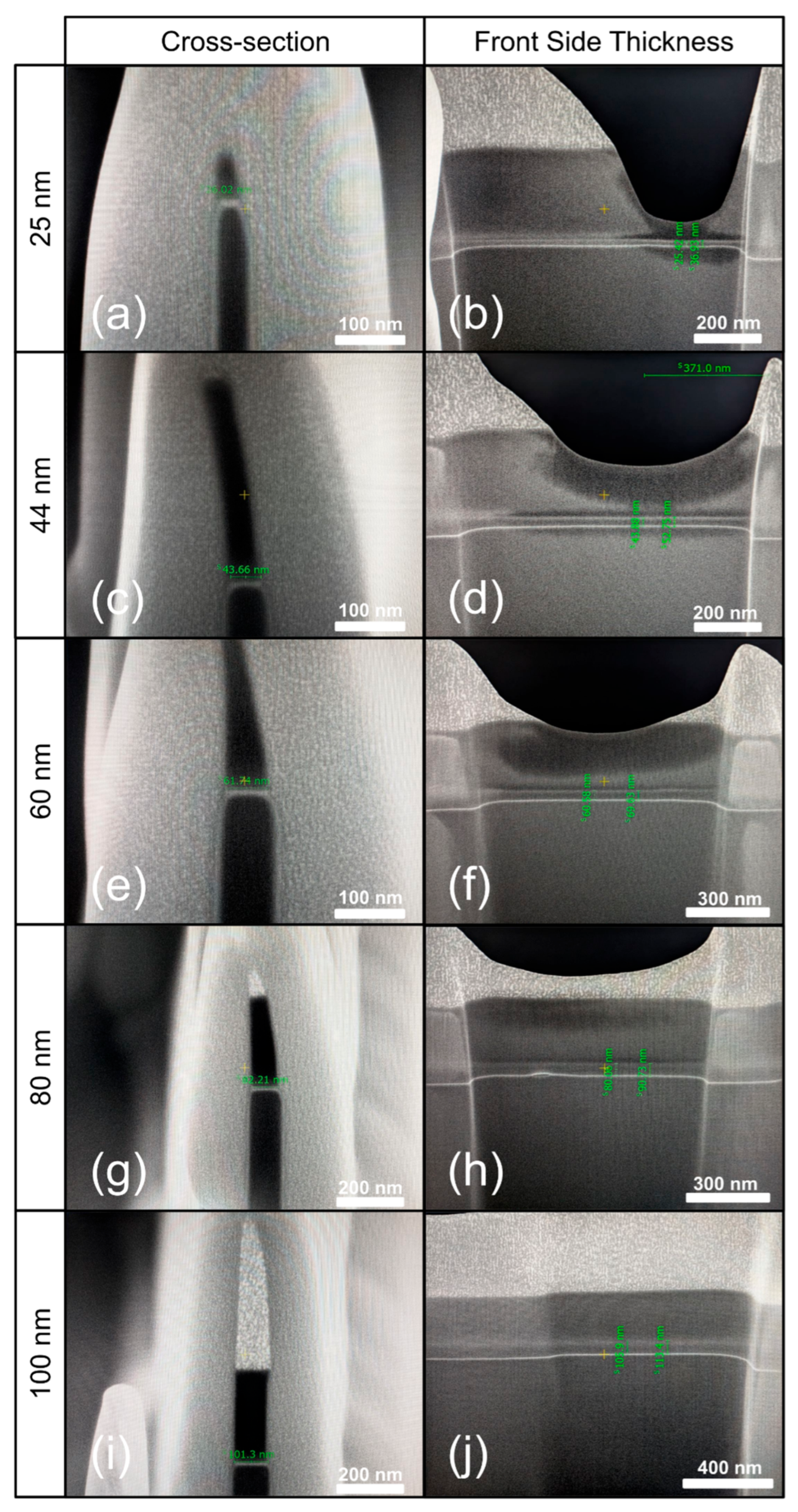
Figure A3.
SEM images for a repeatability analysis for phase# 3. In total, 10 lamellae were all targeted to 32 nm. Figure shows lamellae 1–10 with cross-section measurements and front side SEM image measurements. Measurements shown in Table A2.
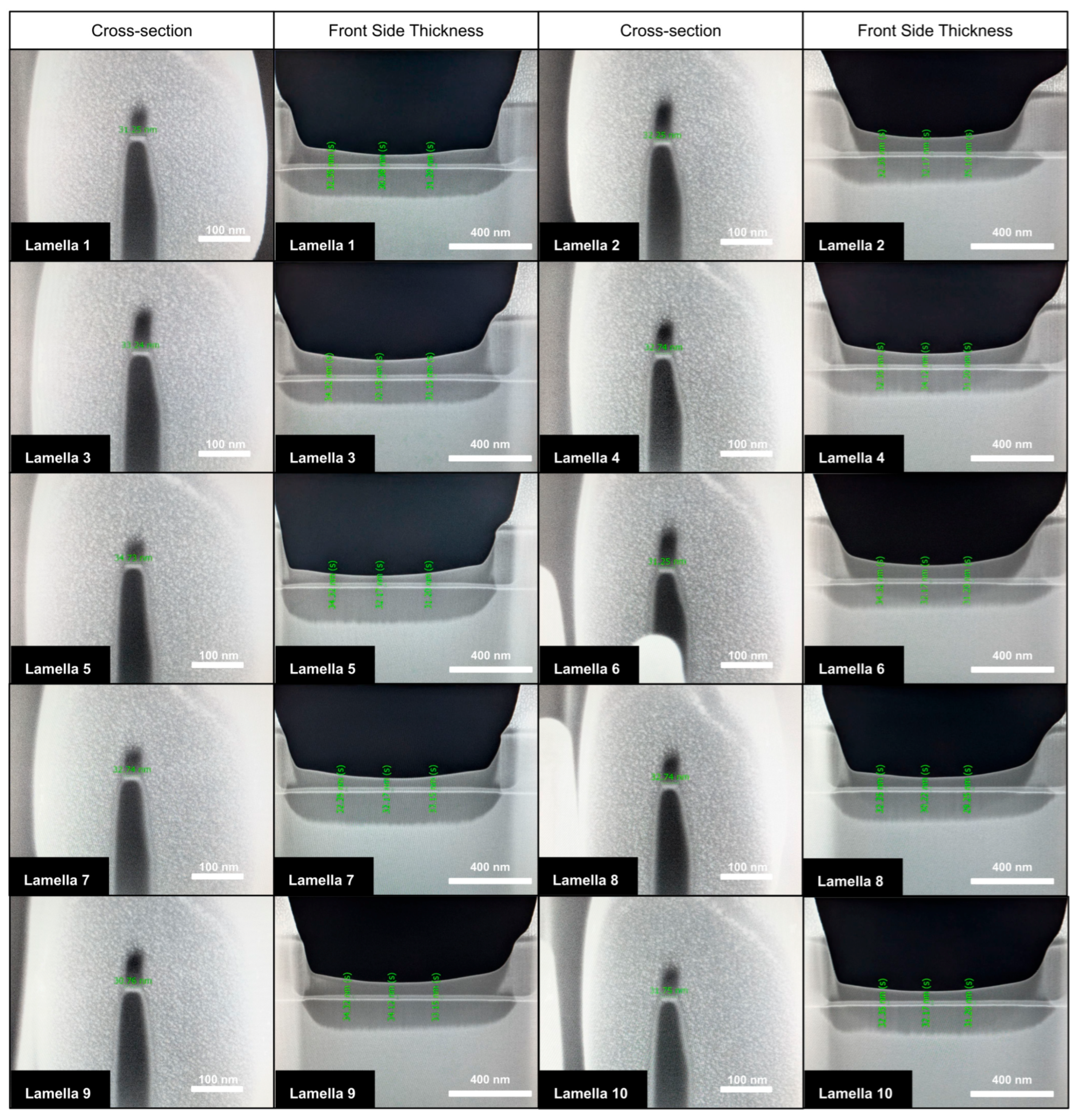
Table A1.
Summary of lamellae targeted and measured thicknesses for phase #2.
Table A2.
Summary of lamellae and cross-sectioned measurements for repeatability study of phase #3.
References
- Mayer, J.; Giannuzzi, L.A.; Kamino, T.; Michael, J. TEM Sample Preparation and FIB-induced Damage. MRS Bull. 2007, 32, 400–407. [Google Scholar] [CrossRef] [Scilit]
- Kim, J.T.; Kim, H.J.; Jo, Y.S.; Choe, S.H. Cross-sectional TEM Specimens Preparation of Precisely Selected Regions of Semiconductor Devices using Focused Ion Beam Milling. Korean J. Mater. Res. 1993, 3, 193–196. [Google Scholar]
- Giannuzzi, L.A.; Stevie, F.A. A review of focused ion beam milling techniques for TEM specimen preparation. Micron 1999, 30, 197–204. [Google Scholar] [CrossRef] [Scilit]
- Lekstrom, M.; McLachlan, M.A.; Husain, S.; McComb, D.W.; Shollock, B.A. Using the in situ lift-out technique to prepare TEM specimens on a single-beam FIB instrument. J. Phys. Conf. Ser. 2008, 126, 012028. [Google Scholar] [CrossRef] [Scilit]
- Bonifacio, C.S.; Ray, M.L.; Fischione, P.E.; Yu, Y.; Skowronski, M. Precise Final Thinning by Concentrated Ar Ion Beam Milling of Plan View TEM Specimens from Phase Change Memory Device Prepared in Xe Plasma FIB. In Proceedings of the ISTFA 2023: Conference Proceedings from the 49th International Symposium for Testing and Failure Analysis, Phoenix, AZ, USA, 12–16 November 2023; pp. 309–316. [Google Scholar] [CrossRef] [Scilit]
- Covalent Metrology. Sample Preparation Orientation and Its Value for Transmission Electron Microscopy. Available online: https://academy.covalentmetrology.com/wp-content/uploads/Episode-24-Slides.pdf (accessed on 29 December 2025).
- Kim, H.J.; Choi, S.; Bae, H.-B.; Lee, T. Transmission Electron Microscopy (TEM) Sample Preparation of Si1–xGex in c-Plane Sapphire Substrate, NASA Technical Memorandum. 2012. Available online: https://ui.adsabs.harvard.edu/abs/2012ntrs.rept13304K/abstract (accessed on 29 December 2025).
- Giannuzzi, L.A.; Stevie, F.A. (Eds.) Introduction to Focused Ion Beams, 1st ed.; Springer: New York, NY, USA, 2005; pp. 73–142. [Google Scholar]
- Tsurusawa, H.; Nakanishi, N.; Kawano, K.; Chen, Y.; Dutka, M.; Van Leer, B.; Mizoguchi, T. Robotic fabrication of high-quality lamellae for aberration-corrected transmission electron microscopy. Sci. Rep. 2021, 11, 21599. [Google Scholar] [CrossRef] [Scilit] [PubMed]
- Tsurusawa, H.; Uzuhashi, J.; Kozuka, Y.; Kimoto, K.; Ohkubo, T. Robust Preparation of Sub-20-nm-Thin Lamellae for Aberration-Corrected Electron Microscopy. Small Methods 2024, 8, e2301425. [Google Scholar] [CrossRef] [Scilit] [PubMed]
- Tsurumi, D.; Doi, T.; Torii, K.; Maruyama, R.; Matsukawa, S. Automating FIB Sample Preparation to Improve STEM Throughput. SEI Tech. Rev. 2019, 89, 56–59. [Google Scholar]
- Tescan: TEM Lamella Preparation with UHR FIB-SEM. Available online: https://info.tescan.com/matsci-fib-sem/applications/tem-sample-preparation (accessed on 31 December 2025).
- Zeiss Crossbeam: Reproducible TEM Lamella Thinning by FIB with Real-Time Thickness Control and End-Point Detection. Available online: https://asset-downloads.zeiss.com/catalogs/download/mic/6263c3cd-da66-4132-b26f-dcb8a048311e/EN_wp_Crossbeam_TEM_Lamella_thinning_FIB.pdf (accessed on 31 December 2025).
- Jeol: Automatic TEM Specimen Preparation System STEMPLING. Available online: https://www.jeolusa.com/PRODUCTS/Focused-Ion-Beam/Specimen-Preparation-System-STEMPLING (accessed on 31 December 2025).
- ThermoFisher Scientific: AutoTEM 5 Software. Available online: https://www.thermofisher.com/us/en/home/electron-microscopy/products/software-em-3d-vis/autotem-5-software.html (accessed on 31 December 2025).
- Uzuhashi, J.; Yao, Y.; Ohkubo, T.; Sekiguchi, T. Experimental investigation and simulation of SEM image intensity behaviors for developing thickness-controlled S/TEM lamella preparation via FIB-SEM. Microscopy 2025, 74, 279–285. [Google Scholar] [CrossRef] [Scilit] [PubMed]
- Conlan, A.P.; Tillotson, E.; Rakowski, A.; Cooper, D.; Haigh, S.J. Direct measurement of TEM lamella thickness in FIB-SEM. J. Microsc. 2020, 279, 168–176. [Google Scholar] [CrossRef] [Scilit] [PubMed]
- Golla-Schindler, U. Quantitative in situ thickness determination of FIB TEM lamella by using STEM in a SEM. In EMC 2008 14th European Microscopy Congress, Aachen, Germany, 1–5 September 2008; Luysberg, M., Tillmann, K., Weirich, T., Eds.; Springer: Berlin/Heidelberg, Germany, 2008. [Google Scholar] [CrossRef] [Scilit]
- Vas, J.V.; Ali, H.; Shi, W.; Denneulin, T.; Gupta, A.K.; Medwal, R.; Dunin-Borkowski, R.E. Quantitative magnetic mapping in TEM through accurate 2D thickness determination. Ultramicroscopy 2025, 275, 114140. [Google Scholar] [CrossRef] [Scilit] [PubMed]
- Lang, C.; Hiscock, M.; Dawson, M.; Hartfield, C. Local thickness and composition analysis of TEM lamellae in the FIB. Microelectron. Reliab. 2014, 54, 1790–1793. [Google Scholar] [CrossRef] [Scilit]
- Boltje, D.B.; Skoupý, R.; Taisne, C.; Evers, W.H.; Jakobi, A.J.; Hoogenboom, J.P. Thickness- and quality-controlled fabrication of fluorescence-targeted frozen-hydrated lamellae. Cell Rep. Methods 2025, 5, 101004. [Google Scholar] [CrossRef] [Scilit] [PubMed]
- Volkenandt, T.; Perez-Willard, F.; Rauscher, M.; Anger, P.M. Towards Automatic Lamella Thinning Using Live Thickness Measurements and Smart End-Point Detection. Microsc. Microanal. 2017, 23, 304–305. [Google Scholar] [CrossRef] [Scilit]
- Iakoubovskii, K.; Mitsuishi, K.; Nakayama, Y.; Furuya, K. Thickness measurements with electron energy loss spectroscopy. Microsc. Res. Tech. 2008, 71, 626–631. [Google Scholar] [CrossRef] [Scilit] [PubMed]
- Tillotson, E.D.I. Assessing Lamellae Thickness During FIB Milling with Monte Carlo Modeling. Master’s Thesis, University of Manchester, Manchester, UK, 2019. Available online: https://pure.manchester.ac.uk/ws/portalfiles/portal/188961862/FULL_TEXT.PDF (accessed on 1 March 2026).
- Hiscock, M.; Dawson, M.; Lang, C.; Hartfield, C.; Statham, P. In-Situ Quantification of TEM Lamella Thickness and Ga Implantation in the FIB. Microsc. Microanal. 2014, 20, 342–343. [Google Scholar] [CrossRef] [Scilit]
- Rakowski, A.; Tillotson, E.; Rooney, A.; Haigh, S. Two Methods for Measuring Lamellae Thicknesses In situ for Improved FIB Specimen Preparation. Microsc. Microanal. 2019, 25, 858–859. [Google Scholar] [CrossRef] [Scilit]
- Simon-Najasek, M.; Huebner, S.; Altmann, F.; Graff, A. Advanced FIB sample preparation techniques for high resolution TEM investigations of HEMT structures. Microelectron. Reliab. 2014, 54, 1785–1789. [Google Scholar] [CrossRef] [Scilit]
- Mierlo, W.V.; Geiger, D.; Robins, A.; Stumpf, M.; Ray, M.L.; Fischione, P.; Kaiser, U. Practical aspects of the use of the X2 holder for HRTEM-quality TEM sample preparation by FIB. Ultramicroscopy 2014, 147, 149–155. [Google Scholar] [CrossRef] [Scilit] [PubMed]
- Zheng, Y.; Yang, X.; Valdes, M.; Davis, A.M.; Heck, P.R. Volume measurement of microparticles using SEM photogrammetry and 3-D reconstruction. Meteorit. Planet. Sci. 2025, 60, 1227–1235. [Google Scholar] [CrossRef] [Scilit]
- Rickard, W.D.; Coelho, J.F.R.; Hollick, J.; Soon, S.; Woods, A. Application of Photogrammetric 3D Reconstruction to Scanning Electron Microscopy: Considerations for Volume Analysis. Electron. Imaging 2021, 33, 60404-1–60404-9. [Google Scholar] [CrossRef] [Scilit]
- Gontard, L.C.; Schierholz, R.; Yu, S.; Cintas, J.; Dunin-Borkowski, R.E. Photogrammetry of the three-dimensional shape and texture of a nanoscale particle using scanning electron microscopy and free software. Ultramicroscopy 2016, 169, 80–88. [Google Scholar] [CrossRef] [Scilit] [PubMed]
- Ball, A.D.; Job, P.A.; Walker, A.E.L. SEM-microphotogrammetry, a new take on an old method for generating high-resolution 3D models from SEM images. J. Microsc. 2017, 267, 214–226. [Google Scholar] [CrossRef] [Scilit] [PubMed]
- Krishna, A.V.; Flys, O.; Reddy, V.V.; Rosén, B.G. Surface topography characterization using 3D stereoscopic reconstruction of SEM images. Metrol. Prop. 2018, 6, 024006. [Google Scholar] [CrossRef] [Scilit]
- Heo, Y.U. Comparative study on the specimen thickness measurement using EELS and CBED methods. Appl. Microsc. 2020, 50, 8. [Google Scholar] [CrossRef] [Scilit] [PubMed]
- Arnoult, C.; Di Martino, J.; Ruch, D. Prediction and limitation of polymer degradation in Environmental SEM. Ultramicroscopy 2012, 122, 32–36. [Google Scholar] [CrossRef] [Scilit] [PubMed]
- Grosso, D.R.; Commisso, M.; Cimino, R.; Larciprete, R.; Flammini, R.; Wanzenberg, R. Effect of the surface processing on the secondary electron yield of Al alloy samples. Phys. Rev. Spec. Top. Accel. Beams 2013, 16, 051003. [Google Scholar] [CrossRef] [Scilit]
- Buban, J.P.; Ramasse, Q.; Gipson, B.; Browning, N.D.; Stahlberg, H. High-resolution low-dose scanning transmission electron microscopy. J. Electron. Microsc. 2010, 59, 103–112. [Google Scholar] [CrossRef] [Scilit] [PubMed]
- Pan, M.; Crozier, P.A. Quantitative imaging and diffraction of zeolites using a slow-scan CCD camera. Ultramicroscopy 1993, 52, 487–498. [Google Scholar] [CrossRef] [Scilit]

Disclaimer/Publisher’s Note: The statements, opinions and data contained in all publications are solely those of the individual author(s) and contributor(s) and not of MDPI and/or the editor(s). MDPI and/or the editor(s) disclaim responsibility for any injury to people or property resulting from any ideas, methods, instructions or products referred to in the content. |
© 2026 by the author. Licensee MDPI, Basel, Switzerland. This article is an open access article distributed under the terms and conditions of the Creative Commons Attribution (CC BY) license.