


Abstract
The development of flexible thin-film transistors (TFTs) is crucial for the advancement of wearable electronics, bendable displays, and the Internet of Things (IoT). A key challenge in this field is the fabrication of high-performance gate dielectric layers that combine excellent electrical properties with mechanical robustness and low-temperature processability. In this work, we report flexible TFTs based on CdS and hybrid PVPh/PMMA-ZrO2 as semiconductor and gate dielectric layers, respectively. The hybrid gate dielectric films were deposited on flexible PEN substrates via a facile spin-coating process at a low temperature of 150 °C. On the other hand, CdS layers were deposited through photo-assisted chemical bath deposition at room temperature. Both correspond to deposition methods in solutions, fulfilling the low-temperature condition. The electrical properties of the hybrid gate dielectric layers were characterized by using metal–insulator–metal (MIM) capacitors, which presented excellent insulating properties, low leakage current density and suitable gate capacitance for transistor operation. From the analysis of the electrical response of flexible TFTs, reliable device characteristics and key electrical metrics were extracted. Furthermore, the MIM and TFTs were tested under mechanical bending, demonstrating stable performance. The MIM capacitors showed outstanding mechanical stability, retaining low leakage and stable capacitance after 1000 bending cycles, with changes attributed to reversible interfacial charge redistribution rather than bulk degradation. Meanwhile the TFTs kept full electrical functionality under repeated bending and tight bending radii (down to 0.6 cm), demonstrating reasonable mechanical durability. These results validate the solution-processed PVPh/PMMA-ZrO2/CdS system as a promising, mechanically robust platform for flexible electronics.
1. Introduction
In recent years, there has been a growing demand for the development of flexible, lightweight, and cost-effective electronic devices. This has accelerated research towards solution-processing fabrication techniques for the deposition of semiconductors and dielectrics layers in thin-film transistors (TFTs) [1,2,3]. Solution-processing techniques offer numerous advantages for the fabrication of flexible TFTs, including reducing manufacturing cost, compatibility with plastic substrates, and scalability of large-area deposition [4]. Unlike conventional vacuum-based deposition methods, solution-processing techniques such as sol–gel spin-coating and inkjet printing methods employ simple and low-cost equipment, delivering higher material utilization efficiency and significantly reducing overall production expenses [5,6]. In addition, these methods can be performed under mild conditions, including low temperatures, which is essential to avoid the thermal degradation of temperature-sensitive flexible substrates such as polyethylene terephthalate (PET) and polyethylene naphthalate (PEN), commonly used in flexible electronic devices [7,8]. Moreover, solution processing offers excellent versatility for the deposition of diverse materials, including organic and inorganic semiconductors and inorganic, polymer, and hybrid dielectric layers [9,10,11,12].
A fundamental component in the performance of TFTs is the gate dielectric, as it strongly impacts the operating voltage, power consumption, and device stability [13]. Though organic dielectrics meet the processing requirements for flexible TFT gate dielectrics, their inherently low dielectric constant and high operating voltage limit their exploitation for high-performance TFTs [14,15]. On the other hand, despite their excellent insulating properties, the high processing temperatures and inherent brittleness of high-k metal oxide dielectrics make their integration into flexible electronics devices challenging [16,17,18,19,20]. To overcome these challenges, the synergistic combination of both types of dielectric materials has emerged as a promising alternative for gate dielectric applications in flexible devices. Organic–inorganic hybrid dielectrics can achieve the required mechanical flexibility and low-temperature processability of polymers (organic phase), with an enhanced dielectric constant delivered by the metal oxides (inorganic phase) [21,22,23,24]. These benefits have encouraged the development of hybrid gate dielectrics for TFTs. Representative hybrid dielectric systems include polymer matrices such as polymethyl methacrylate (PMMA), polyvinyl pyrrolidone (PVP), and poly 4-vinylphenol (PVPh) blended with high-k metal oxides such as TiO2, ZrO2, HfO2, and Al2O3 [25,26,27,28,29,30,31,32]. These hybrid nanocomposites have demonstrated enhanced dielectric properties, positioning them as highly stable and promising dielectric candidates for TFT applications [33].
Solution processing of hybrid dielectrics provides additional advantages by enabling the facile blending of multiple organic and inorganic phases into a single hybrid dielectric layer with enhanced material properties. For example, the strategic combination of PMMA and PVPh results in an organic composite material that overcomes the individual performance limitations of each polymer, leading to tunable gate dielectrics for TFTs [34]. In this blend, the non-polar and linear molecular structure of PMMA provides excellent insulating properties, and it dilutes the concentration of hydroxyl groups of PVPhs. This disrupting ion conduction pathway significantly reduces gate leakage current and increases dielectric strength compared to pure PVPh. Additionally, the incorporation of PMMA helps passivate electron trap states associated with PVPhs, leading to a dramatic reduction in interfacial trap density, and improves the charge transport dynamics in TFTs. The blended dielectric offers superior surface morphology, smoother films, more flexibility, and more pinhole-free films than pure PVPh films. Such surface features are essential for high-quality semiconductor growth and the formation of an excellent dielectric/semiconductor interface, which result in a steeper subthreshold swing and higher charge carrier mobility, and can even enable n-type or ambipolar operation in semiconductors that are typically restrained to p-type behavior on pure PVPh. Furthermore, since PVPh has one of the highest dielectric constant values (∼4.5) among the dielectric polymers, this polymer blend allows for an increase in k to values higher than those of pristine PMMA (∼3.5). This directly impacts the capacitance of the gate dielectric and therefore the transistor’s current output, which is a key factor in the device performance [35]. Therefore, the PVPh/PMMA blend constitutes an organic gate dielectric material, whose properties can contribute to the exceptional reliable device performance required for advanced flexible electronic applications.
Based on the benefits of the PVPh/PMMA blend, we report here its use as the organic phase in an organic–inorganic hybrid dielectric system incorporating zirconium dioxide (ZrO2) as the inorganic phase for flexible TFT applications. ZrO2 is a high-k dielectric material (~25) with a wide band gap (~5.1–5.9 eV) and excellent thermodynamic stability [36,37]. The resulting PVPh/PMMA-ZrO2 hybrid system leverages both classes of dielectric materials, combining the mechanical flexibility, low processing temperature, and appropriate interfacial properties of the polymer phase with the high gate capacitance density, low leakage current and smooth surface morphology of the ZrO2. Additionally, hybrid dielectric materials are compatible with a wide range of metal oxides and chalcogenide-based semiconductors and demonstrate significant electrical performance in TFTs. Recently, chalcogenide semiconductors, such as CdS, PbS, and CdSe, have gained attention as a window layer in solar cells or active layer in LEDs and TFT devices [38,39,40,41]. Among them, CdS is considered a great choice as an active layer in TFTs due to its ease of deposition through chemical bath deposition (CBD). The CBD process typically occurs at low temperatures (60–90 °C), making it highly compatible with flexible plastic substrates. Moreover, as a semiconductor, CdS inherently performs reliable n-type conductivity, capable of achieving high electron mobility (1–10 cm2/V·s) and strong electrical switching speed with on/off current ratios of up to 106 [42,43,44].
In this work, we first report on the synthesis process of hybrid films and analyze their properties. The PVPh/PMMA-ZrO2 hybrid gate dielectric was selected due to its simple and low-temperature solution process, which permits deposition on flexible PEN/ITO substrates, where ITO (Indium tin oxide) plays the role of the device’s common bottom gate [45,46]. The hybrid thin films were prepared from sol–gel precursor solutions through a spin-coating process followed by thermal annealing at a low temperature of 150 °C. To assess their dielectric performance, flexible MIM capacitors were fabricated and electrically analyzed. To further demonstrate the feasibility of PVPh/PMMA-ZrO2 hybrid thin films as a gate dielectric layer, bottom-gate solution-processed flexible TFTs were fabricated with CdS, deposited through photo-assisted CBD at room temperature, and utilized as the semiconductor channel layer. This fully solution-processed approach significantly reduces fabrication complexity and cost while maintaining compatibility with low temperatures, marking a significant step towards scalable high-performance flexible electronics.
2. Materials and Methods
2.1. Preparation and Characterization of Hybrid Dielectric
The PVPh/PMMA-ZrO2 hybrid dielectric layers were prepared using precursor solutions, obtained by separately mixing organic and inorganic solutions. All chemicals and reagents mentioned below were purchased from Sigma-Aldrich (St. Louis, MO, USA), unless otherwise specified. The PMMA phase was obtained through the in-situ polymerization of methyl methacrylate (MMA, MW = 100.1 g/mol, ρ = 0.936 g/mL), prepared at a monomer concentration of 0.180 M, which corresponds to the concentration of repeat units. Benzoyl peroxide was used as the initiator under magnetic stirring at 60 °C for 60 min. The PVPh solution was prepared by dissolving 10 mM PVPh (MW = 11,000 g/mol) in propylene glycol monomethyl ether acetate (PGMEA) as a solvent. Simultaneously, 1 mM of the cross-linker polymelamine-co-formaldehyde (PMF) was added to this solution to reduce the hydroxyl group concentration, and the final solution was stirred for 6 h under ambient temperature. The final organic phase of the PVPh/PMMA solution was obtained by mixing the PMMA and PVPh solutions at equal volumes (50/50 v/v%) and stirring for one hour to obtain a homogeneous solution. The inorganic ZrO2 solution was prepared using zirconium chloride (ZrCl4, 99.99%) as a precursor. A 0.2 M solution of ZrCl4 in ethanol (99.99% J. T. Baker, Phillipsburg, NJ, USA) was mixed, and nitric acid (HNO3, 65% J. T. Baker, Phillipsburg, NJ, USA) and deionized water (DI) were added sequentially to achieve a final molar ratio of 1:100:10:10. The solution was then agitated at 60 °C for 4 h to promote hydrolysis and condensation, forming the inorganic network. Finally, the hybrid precursor solution was obtained by mixing the organic and inorganic solutions in equal volumes (50/50 v/v%) and stirring for 6 h at room temperature to ensure homogenization. The precursor molar ratios in the hybrid system are PVPh:PMMA:ZrO2 ≈ 10 mM:180 mM:200 mM, and when normalized to Zr, the molar ratio is PVPh:PMMA:ZrO2 ≈ 0.05:0.90:1.
The deposition of PVPh/PMMA-ZrO2 hybrid dielectric films was performed by spin-coating at 5000 rpm for 30 s onto ITO-coated PEN flexible substrates. Subsequent processing involved drying the wet-gel films at 100 °C for 5 min on a hot plate for removal of residual solvent, followed by thermal annealing at 150 °C for 3 h in air to induce cross-linking and densification. The resulting hybrid films were uniform, transparent, and adhered very well to the substrate. Their chemical bonding, optical characteristics, and surface morphology were analyzed using FTIR, UV-Vis spectroscopy, and AFM. For the evaluation of the dielectric properties, metal–insulator–metal (MIM) capacitors were assembled with hybrid layers as insulators. For this, after deposition, circular gold top contacts were evaporated onto hybrid films. Capacitance versus frequency and current versus voltage measurements were performed to obtain dielectric constant and leakage current characteristics.
2.2. Fabrication and Characterization of CdS-Based Flexible TFTs
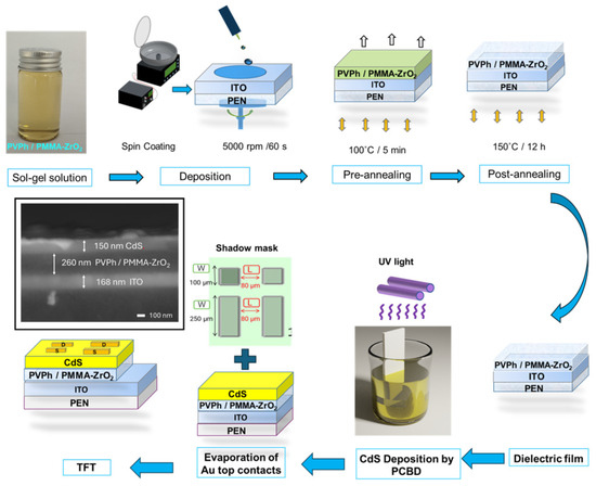
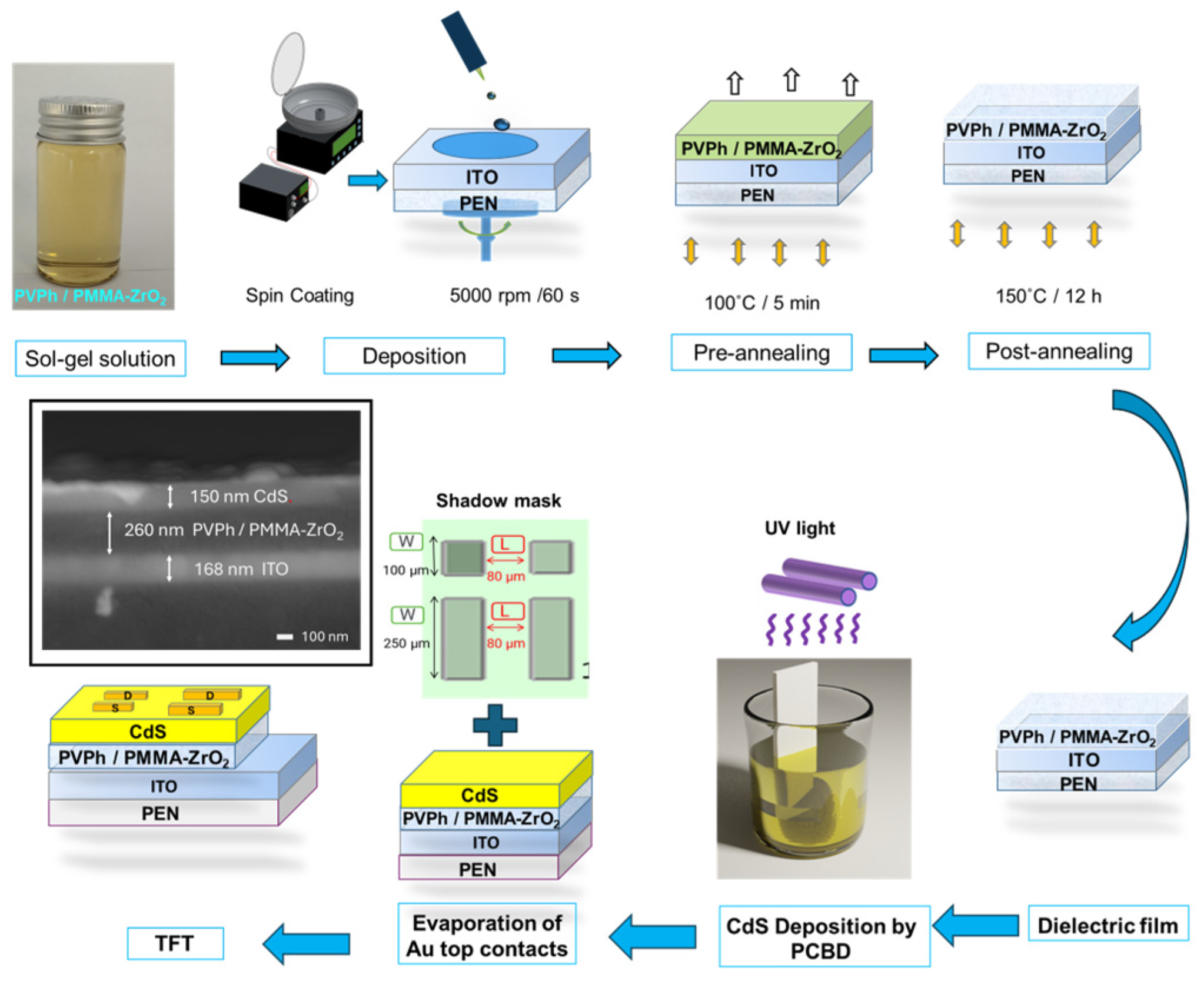
For CdS TFT fabrication, all chemicals and reagents used for the CdS chemical bath deposition were purchased from J.T. Baker (Phillipsburg, NJ, USA), unless otherwise specified. The reaction bath for the chemical bath deposition solution (CBD) process was prepared in a 50 mL beaker through the sequential addition of 7.5 mL of 0.05 M CdCl2 (cadmium chloride), 7.5 mL of 0.5 M C6H5O7Na3O7.2H2O (sodium citrate), 2.5 mL of 0.5 M KOH, 2.5 mL of a pH 10 borate buffer, and 3.75 mL of 0.5 M CS(NH2)2 (thiourea). The solution was diluted to make a total volume of 50 mL using DI water. The CdS semiconductor layer was deposited onto hybrid dielectric layers using the photo-assisted CBD process at room temperature for 4 h to obtain the desired film thickness [47,48]. For this, the reaction solution was irradiated with a 313 nm UV lamp during the film deposition [42]. Finally, to complete the bottom-gate flexible CdS-based TFT fabrication process, patterned Au source and drain contacts, with channel dimensions of 250 μm (width) and 80 μm (length), respectively, were evaporated through a shadow mask via thermal evaporation. The electrical response of the assembled flexible TFTs was analyzed using current versus voltage, output and transfer characteristics measured with a 4200 Keithley (Solon, OH, USA) semiconductor parameter analyzer. Figure 1 shows the schematic illustration of the CdS TFT fabrication process.
Figure 1.
Scheme of the CdS-based TFT fabrication process with PVPh/PMMA-ZrO2 hybrid gate dielectrics. The inset displays the cross-sectional SEM image of the assembled device.
3. Results
3.1. PVPh/PMMA-ZrO2 Hybrid Layers Characteristics
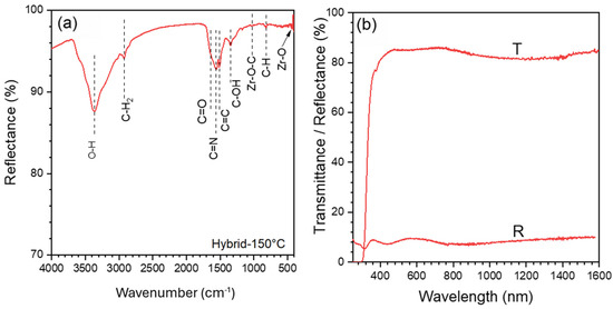
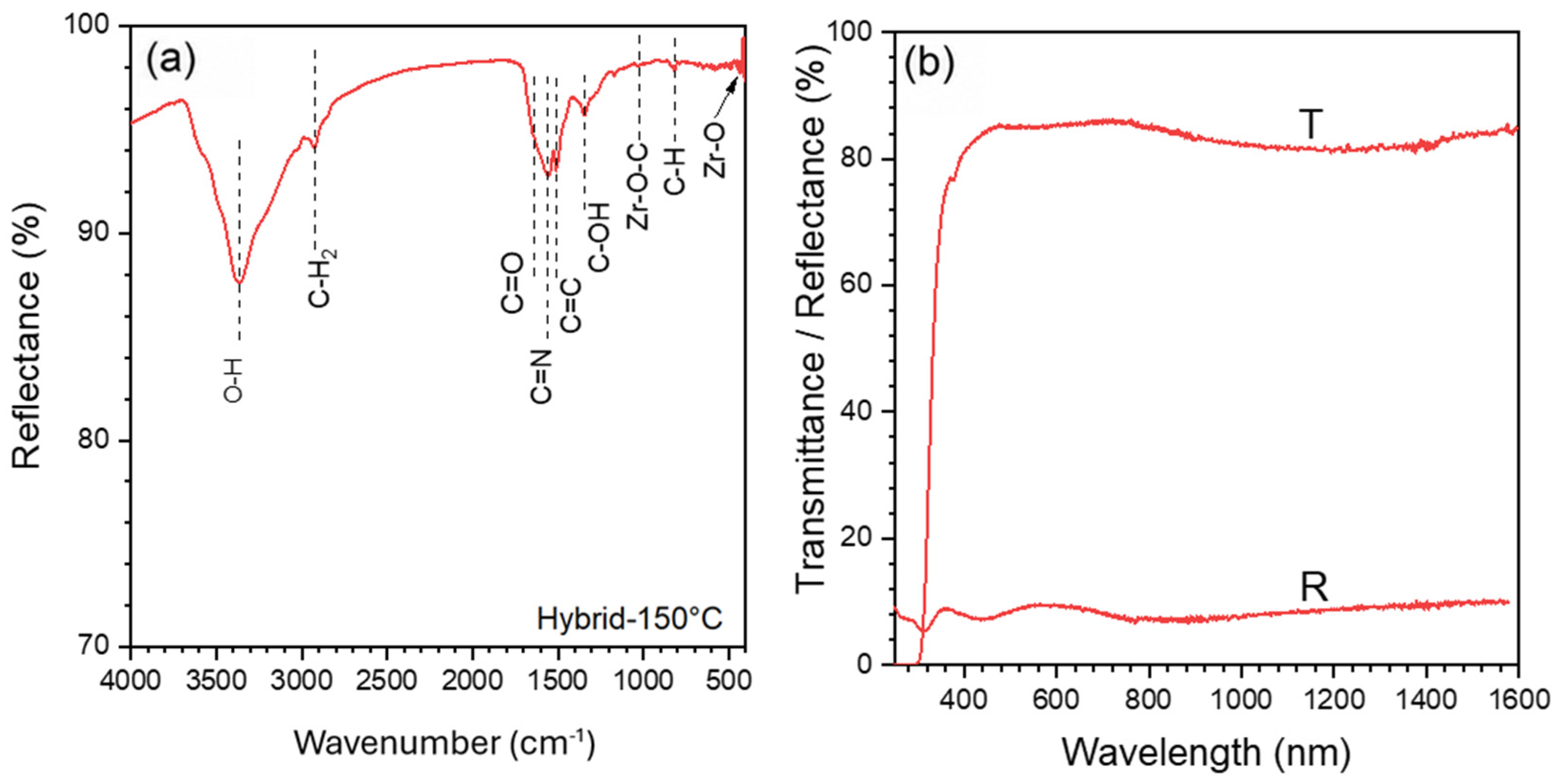
The formation of the hybrid cross-linked organic and inorganic phases at the molecular scale was corroborated by FTIR analysis. Figure 2a shows the FTIR spectra of the PVPh/PMMA-ZrO2 hybrid dielectric film in the wavenumber range from 400 to 4000 cm−1. Characteristic functional groups of the material’s organic constituents are clearly identified in the FTIR spectrum. The most intense broad band at 3350 cm−1 is associated with hydroxyl (-OH) stretching vibration modes. These groups originate from the incomplete condensation of the inorganic phase during the sol–gel processing and/or from the tail of PMF molecules used for the cross-linking of the PVPh phase. The narrow band at 2930 cm−1 is assigned to the asymmetric stretching vibrations of -CH2 groups in the PVPh/PMMA copolymer [49,50]. A small shoulder at 1770 cm−1, characteristic of the PMMA phase, is correlated with C=O carbonyl stretching. The presence of PVPh is confirmed by peaks at 1625 cm−1 (C-C), 1340 cm−1 (C-OH), and 1075 cm−1 (C-O) [51]. Furthermore, the cross-linker PMF is identified by its distinctive peaks at 1536 cm−1 and 1170 cm−1, corresponding to aromatic C=N and branching C-N stretching vibrations, respectively [52]. Thus, the FTIR analysis confirmed the presence of all organic components and the cross-linker. Regarding the inorganic phase, the characteristic Zr-O stretching vibration, which typically appears below 700 cm−1, is observed as a weak peak below 500 cm−1 due to the detection limit of the instrument at low wavenumbers. This, along with the O-H signal from the incomplete condensation of the inorganic phase, provides definitive evidence of the formation of an inorganic phase in the hybrid network. Furthermore, there is another weak signal at 1030 cm−1 attributed to Zr-O-C groups. This not only confirms the presence of the inorganic phase but also provides direct evidence for molecular-scale cross-linking between the zirconia network and the polymer chains, consistent with findings from similar PVPh–zirconia hybrid systems [53].
Figure 2.
(a) FTIR spectrum and (b) transmittance and reflectance spectra of the PVPh/PMMA-ZrO2 hybrid dielectric layer.
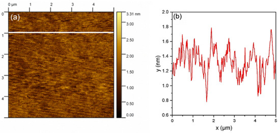
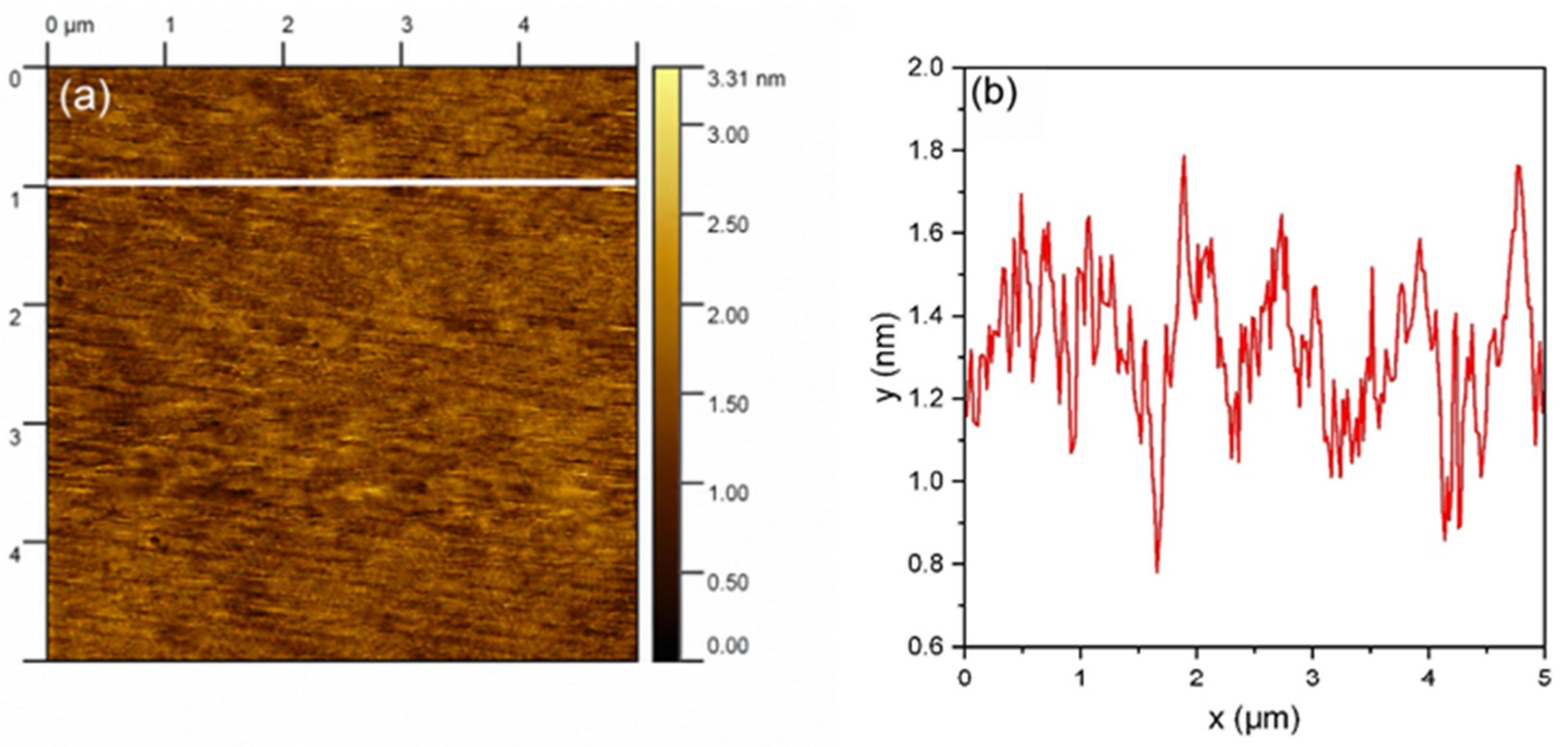
The optical properties of the hybrid films were characterized by measuring their transmission (T) and reflection (R) spectra across the 240–1600 nm wavelength range, as shown in Figure 2b. A key finding is the high transparency of the films, which display an average transmittance of approximately 86% in the visible spectrum (380–750 nm), with a corresponding average reflectance of about 8.8%. The optical transmittance goes further to the IR region. Crucially, the sum of (T + R) is close to 100%, indicating negligible light scattering and absorption losses. This optically lossless behavior macroscopically validates the formation of a well-integrated hybrid network at the microscopic scale, with no significant phase separation. Atomic force microscopy (AFM) corroborates this structural homogeneity, as shown in Figure 3a, where the 5 × 5 μm2 image displays a smooth and uniform surface with a very low roughness of 0.3 nm. The structural domains in the smooth, homogeneous surface observed in the AFM image are at the nanometric scale. The height profile of the horizontal line across the surface of the hybrid film shown in Figure 3b makes the hybrid surface smoothness more evident, with maximum and minimum heights separated by less than 1 nm. These surface microscopic features of the hybrid film surface are consistent, with no phase separation. The confluence of these high-transparency, low-scattering, and smooth-surface characteristics renders these hybrid films ideally suited for use as gate dielectrics with no appreciated agglomeration and very low root-mean-square (RMS) surface roughness. An RMS surface roughness value below 1 nm is highly encouraging for creating a high-quality dielectric/semiconductor.
Figure 3.
(a) AFM image of the surface of the PVPh/PMMA-ZrO2 hybrid dielectric layer. (b) Height profile along the white horizontal line shown in the AFM image.
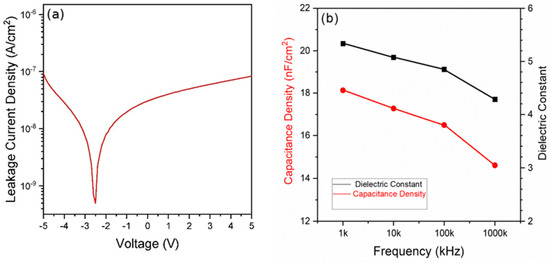
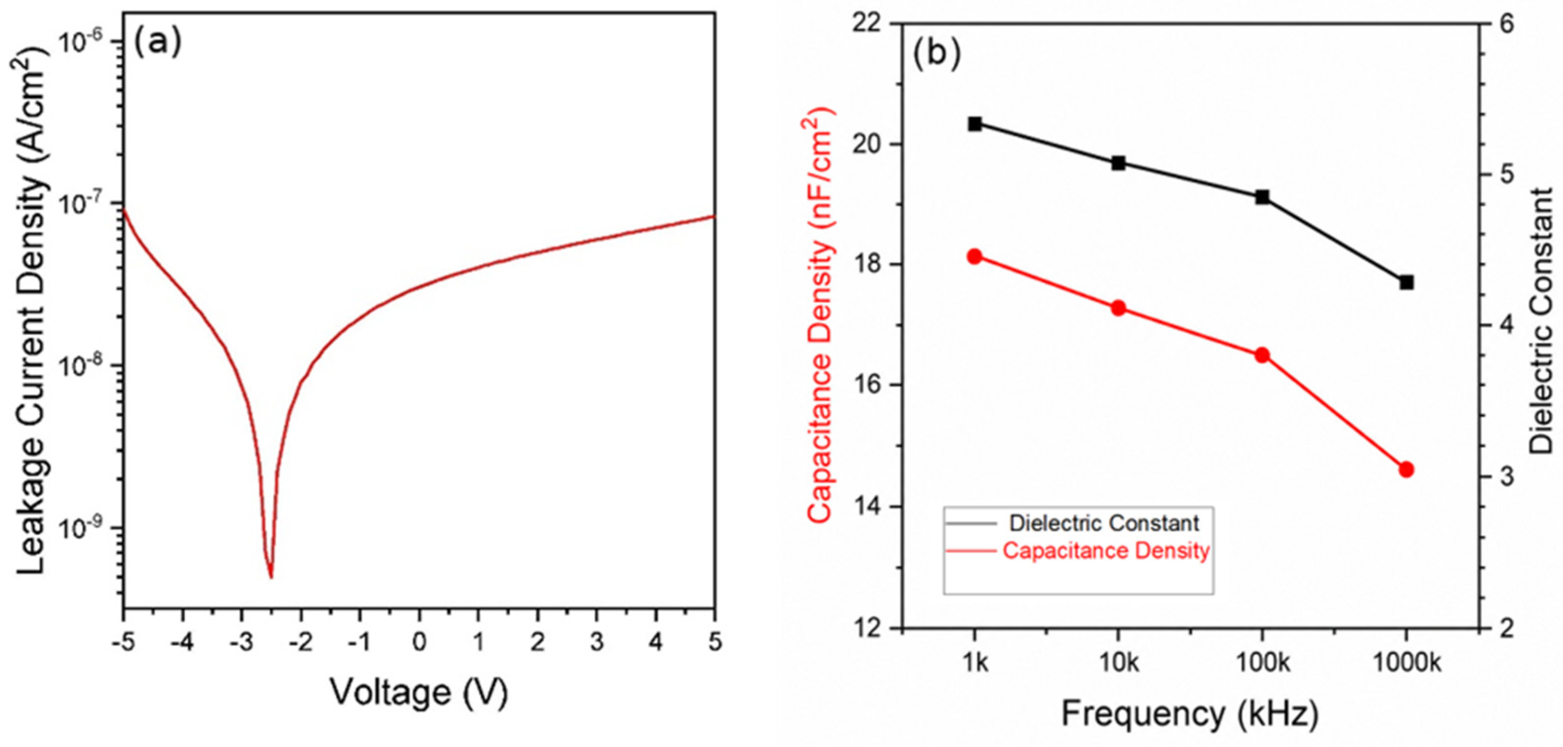
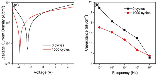
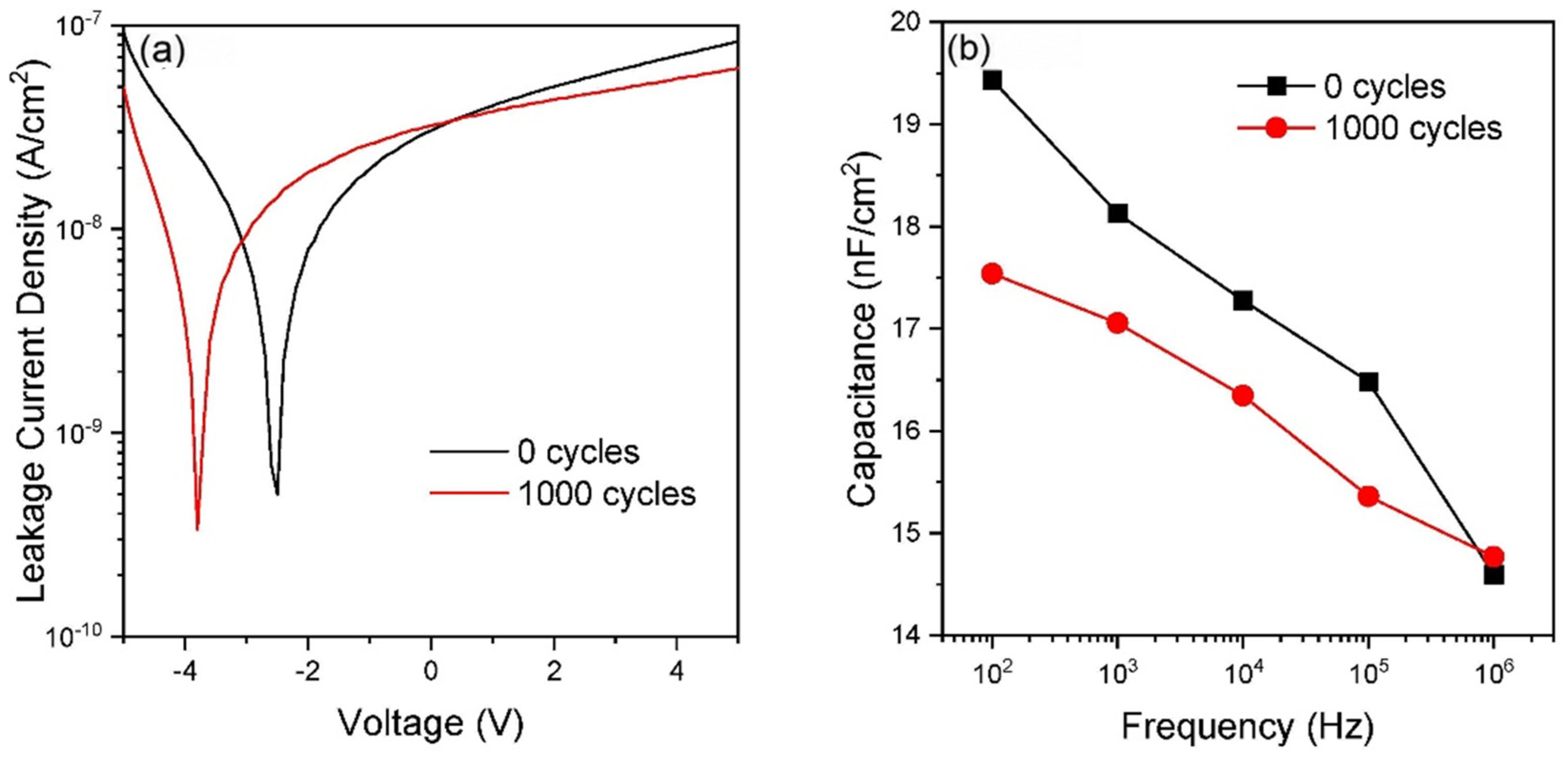
The dielectric properties of the PVPh/PMMA-ZrO2 hybrid layers were characterized using current–density–voltage (I–V) and capacitance–frequency (C-f) measurements from metal–insulator–metal (MIM) capacitors. Figure 4a presents the leakage current density as a function of the applied voltage (−5 V to 5 V). The hybrid films exhibit a low leakage current density slightly below 10−7 A/cm2 at the maximum voltage. The I–V characteristic of the MIM device is asymmetric, with the minimum current shifted by −2.5 V. This shift is likely due to electron traps from oxygen defects and highly polarizable OH groups, which create an internal electric field [25]. The low leakage current values demonstrate that these hybrid dielectric layers are suitable for use as gate insulators in thin-film transistor fabrication. On the other hand, Figure 4b (left y-axis, red dots) shows the C-f measurements carried out on MIM capacitors from 1 kHz to 1 Mhz at 0 V applied voltage. It is observed that there is a decreasing trend in capacitance as the frequency increases, reflecting a dependence on the temporal response of the different polarization mechanisms in the hybrid dielectric layers. From the capacitance results, the dielectric constant of the hybrid layer was determined using the relation Ci = (ε0 k)/d, where ε0 is the vacuum permittivity, k is the dielectric constant, d represents the dielectric layer thickness and Ci is the capacitance per unit of area. Figure 4b (right y-axis, black dots) shows the dielectric constant of the hybrid dielectric layer as a function of frequency. The dielectric constant at 1 kHz is 5.4, which is quite appropriate for gate dielectric applications. To assess the mechanical stability of the gate dielectric and ITO/PEN substrate, the MIM flexible capacitors were also characterized before bending and after 1000 bending cycles. The results are shown in Figure 5. The leakage current density remained at comparable levels after bending (Figure 5a), showing only a slight reduction and a shift in the minimum current toward more negative voltages. Moreover, capacitance versus frequency measurements (Figure 5b) revealed a moderate decrease in capacitance density at low frequency, from approximately 19.5 nF/cm2 (initial state) to ~17.5 nF/cm2 at 100 Hz after 1000 bending cycles, while the capacitance at high frequency (≈1 MHz) remained essentially unchanged at ~15 nF/cm2. These results suggest that mechanical bending primarily affects slow polarization processes or interfacial charge trapping and may be associated with mechanically induced redistribution of trapped charge in the electrode–dielectric interface.
Figure 4.
(a) Leakage current density versus voltage and (b) capacitance density and dielectric constant versus frequency of the PVPh/PMMA-ZrO2 hybrid dielectric layer measured in the MIM devices.
Figure 5.
(a) Leakage current density versus voltage and (b) capacitance density versus frequency of the PVPh/PMMA-ZrO2 hybrid dielectric before and after 1000 bending cycles.
3.2. Electrical Response of the CdS TFTs with PVPh/PMMA-ZrO2 Hybrid Gate Dielectric
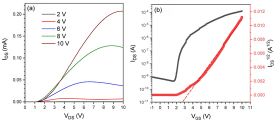
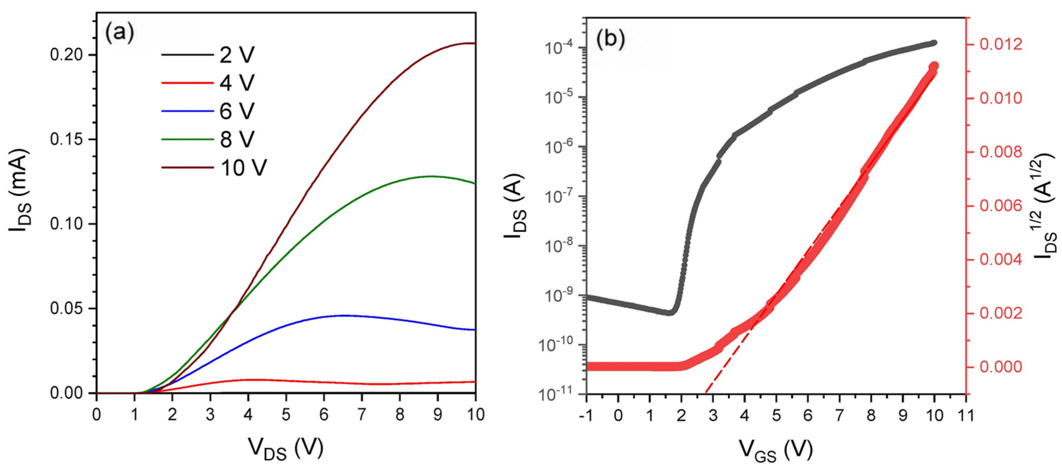
Leveraging the favorable dielectric properties of the PVPh/PMMA-ZrO2 hybrid thin films for gate dielectric applications, we fabricated thin-film transistors (TFTs) using solution-processed (CBD) CdS as the channel layer. Both the dielectric and semiconducting layers were deposited via solution-based methods. The devices employed a bottom-gate, top-contact structure, as illustrated in Figure 1. The thickness of the dielectric gate and semiconductor layers were 260 and 150 nm, respectively. The electrical performance of these CdS-based TFTs is presented in Figure 6. The output IDS versus VDS curves are shown in Figure 6a. These curves were measured with a drain voltage (VDS) swept from 0 to 10 V at gate voltage (VGS) steps of 2 V (2 to 10 V) and exhibit classic n-type behavior. At low drain voltages, the drain current increases linearly, followed by a clear pinch-off and saturation at higher voltages. However, a rightward shift in the linear regime is observed, a characteristic often attributed to the presence of parasitic contact resistance at the source and drain electrodes, which reduces the effective voltage across the semiconductor channel.
Figure 6.
(a) Output and (b) transfer curves of the CdS-based TFTs with PVPh/PMMA-ZrO2 hybrid dielectric gate layer. In (b), the black and red curves correspond to IDS (left y-axis) and IDS1/2 (right y-axis), respectively.
The corresponding transfer characteristics (IDS-VGS), measured in the saturation region at VDS = 8 V, are shown in Figure 6b (left y-axis). In this curve, the drain current at low voltage (off current) is around 10−9 A, increasing at higher voltages up to values of 10−4 A (on current), which corresponds to an Ion/Ioff ratio of 105. The field-effect mobility (μ) and threshold voltage (VT) of the devices were extracted from the transfer curves (Sqrt IDS vs. VGS; right y-axis of Figure 6b by fitting the data in the saturation regime to the standard equation IDS = (W/2L) μ C (VGS − VT)2, where W and L are the channel width and length, and C is the areal capacitance of the dielectric layer. The μ and VT values were determined from the slope and the x-intercept of the extrapolated linear fit to the data, shown as the dashed line in the plot. A set of 10 devices was measured, and the average values of μ and VT were 79 ± 17 cm2/V·s and 4.3 ± 0.9 V, respectively. Furthermore, the subthreshold swing, SS, of the devices was also determined from the transfer curves in the saturation regime using Equation (1):
An average SS value of 456 mV/dec ± 158 mV/dec was obtained from the set of measured devices. Also, based on this SS value, the interface trap density was estimated using the conventional subthreshold swing model, assuming negligible depletion capacitance, which is a common approximation for thin-film transistors. The interface trap density, Dit, was estimated using the following Equation (2):
where T is the temperature, k is the Boltzmann constant, and q is the elementary charge. The Dit estimated value was 1012 cm−1eV−1. All these device parameters indicate promising performance for flexible electronics. The high mobility, in particular, is notable for a solution-processed device. However, it is important to consider that the extracted mobility value may be influenced by contact effects.
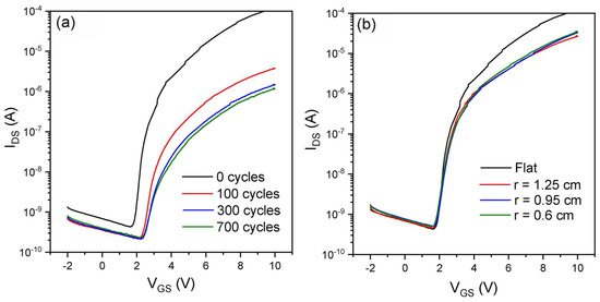
The TFTs were also subjected to cyclic bending from 0 up to 700 cycles, and their transfer characteristics were recorded after mechanical stressing. The devices retained characteristic TFT operation throughout the bending tests, as observed in Figure 7a. While a gradual degradation was observed with an increasing number of bending cycles, the devices remained electrically functional. The apparent field-effect mobility decreased from approximately 79 cm2/V·s in the initial state to about 1 cm2/V·s after 700 bending cycles, while the threshold voltage exhibited only a modest shift from ~3.7 to ~3.8 V. In addition, the electrical response of the TFTs was evaluated under different bending radii of 1.25, 0.95 and 0.6 cm, as shown in Figure 7b. As observed, stable transistor operation was maintained even at the smallest bending radius of 0.6 cm. Under this condition, the apparent mobility decreased from ~79 cm2/V·s (flat state) to ~20 cm2/V·s, while the on-state current decreased slightly but remained within the same order of magnitude. Notably, no significant threshold voltage shift was observed as a function of the bending radius. These results indicate that the ITO gate on PEN maintains electrical continuity and gate functionality during mechanical deformation, and that the hybrid dielectric/CdS TFT structure exhibits reasonable mechanical durability under repeated bending. The observed degradation is attributed to accumulated mechanical strain in the ITO/PEN substrate and at the dielectric/semiconductor interface. Further optimization of electrode materials and interfaces will be pursued in future work to improve mechanical endurance.
Figure 7.
(a) Transfer curves of the CdS-based TFTs with PVPh/PMMA-ZrO2 hybrid dielectric gate layer measured before and after 100–300 bending cycles. (b) Transfer curves measured under bending at different bending radii.
4. Discussion
4.1. Correlation of Hybrid Dielectric Properties and Performance
The electrical performance of the CdS-based TFTs can be attributed to the superior properties of the PVPh/PMMA-ZrO2 hybrid gate dielectric. The optical, structural, and electrical characterizations collectively confirm the formation of a high-quality, well-integrated hybrid network. The high optical transparency (~86%) and the near-100% sum of transmittance and reflectance indicate an optically lossless film with minimal light scattering, which macroscopically suggests excellent morphological homogeneity. This is conclusively verified by AFM, which reveals an ultrasmooth surface with a root-mean-square (RMS) roughness of only 0.3 nm. This level of smoothness is critical, as it minimizes charge carrier scattering and trapping at the dielectric/semiconductor interface, which is a primary prerequisite for achieving high field-effect mobility. Furthermore, FTIR analysis provides definitive evidence of the molecular-scale integration between the organic and inorganic phases. The presence of the Zr-O-C vibration mode at 1030 cm−1 is particularly significant, as it confirms covalent cross-linking between the zirconia network and the polymer chains. This cross-linked structure is fundamental in enhancing the mechanical robustness of the film and attenuating large-scale phase separation, which directly contributes to its excellent electrical integrity. The dielectric characterization further underscores the suitability of this material for TFT applications. The measured leakage current density below 10−7 A/cm2 is sufficiently low to ensure that gate leakage does not compromise the switching characteristics of the TFT. The observed frequency dispersion in capacitance, a common trait in polymeric and hybrid dielectrics, is attributed to the contribution of various polarization mechanisms. The dielectric constant of 5.4 at 1 kHz is well suited for gate dielectrics, providing a strong capacitive coupling without the excessive electric fields that can lead to high leakage in very-high-k materials. The mechanical stability assessment of the flexible PVPh/PMMA-ZrO2 hybrid dielectric capacitors demonstrated their robustness for flexible electronics. After 1000 bending cycles, the dielectric maintains a low leakage current, confirming its structural integrity and unaltered insulating properties. The accompanying minor shift in the current–voltage characteristic suggests that bending redistributes trapped charges at the electrode interface, modifying the internal electric field. Capacitance measurements reveal that bending selectively reduces low-frequency capacitance while leaving high-frequency capacitance unchanged. This indicates that mechanical stress does not damage the material’s fundamental bulk polarization but specifically impedes slower interfacial polarization mechanisms, likely by reorganizing trapped charges at interfaces. Overall, the dielectric exhibits excellent mechanical stability, with only minimal, reversible changes linked to interfacial charge dynamics, affirming its suitability for flexible thin-film transistors.
4.2. Analysis of Thin-Film Transistor Performance
The TFTs fabricated using this hybrid dielectric exhibited promising performance metrics. The high Ion/Ioff ratio of 105 is a direct consequence of the low leakage current of the dielectric and the good semiconducting properties of the CdS channel, confirming the device’s excellent switching capability and potential for low-power applications. The extracted average field-effect mobility of 79 cm2/V·s is exceptionally high for a solution-processed TFT and is competitive with many devices fabricated on rigid substrates. We attribute this high mobility to two key factors: (1) the ultrasmooth interface between the hybrid dielectric and the CdS channel, which minimizes scattering centers, and (2) the high capacitance of the dielectric, which induces a high charge density in the channel at a given gate voltage. However, a critical analysis necessitates addressing the non-ideality observed in the output characteristics. The distinct rightward shift in the linear regime is a classic signature of significant parasitic contact resistance at the source/drain electrodes. This resistance causes a voltage drop that reduces the effective voltage across the channel, leading to an underestimation of the drain current in the linear region. Consequently, the standard saturation-region mobility extraction model, which does not account for the contact resistance, can overestimate the true channel mobility. Therefore, while the reported value of 79 cm2/V·s indicates outstanding performance, it likely represents an upper limit, and the actual channel mobility may be lower once contact effects are de-embedded. Furthermore, while the reported field-effect mobility (79 cm2/V·s) is relatively high for solution-processed CdS TFTs, it remains within the upper range reported for this material system in the literature. For example, Rao et al. [43] reported a mobility of 36.1 cm2/V·s in fully solution-processed CdS TFTs using a PVP-based hybrid gate dielectric, while in previous work we reported mobilities as high as 64.4 cm2/V·s in CdS TFTs employing a low-temperature Al2O3–GPTMS–PMMA hybrid dielectric [42]. Moreover, Weimer reported an evaporated CdS-TFT with mobilities of up to 140 cm2/Vs [54]. Thus, the extracted mobility of the CdS-based flexible devices remains representative of the high-performance regime achievable with the present material system. On the other hand, the positive, not so high, average threshold voltage of 4.3 V indicates normally off (enhancement-mode) operation, which is desirable for digital circuits to minimize power consumption in the off state. Taking as the metric of the threshold voltage variation its standard deviation, ± 0.9 V, we can say that this is acceptable, yielding values between 3.4 and 5.2 V. The origin of this positive VT can be linked to the dielectric/semiconductor interface quality. The presence of electron traps, potentially arising from the hydroxyl groups identified in the FTIR analysis or from interface states, can pin the Fermi level and shift the VT in the positive direction. The cyclic bending tests of the TFTs demonstrated promising mechanical durability while highlighting key degradation modes. The devices maintain full functionality throughout 700 bending cycles and down to a tight 1.2 cm radius, confirming the structural integrity of the ITO gate and the overall hybrid dielectric/CdS architecture. However, a significant, progressive degradation in performance is observed, most critically in the field-effect mobility, which drops drastically (from ~79 to ~1 cm2/V·s) over repeated bending. This suggests that accumulated mechanical strain primarily damages the charge transport pathway, likely at the dielectric/semiconductor interface or within the semiconductor layer itself. Notably, the threshold voltage remains remarkably stable under both cyclic and static bending, indicating minimal creation of new bulk traps in the dielectric or at the critical gate interface. The results therefore distinguish between two failure mechanisms: reversible strain-induced mobility reduction (seen in radius-dependent tests) and cumulative, irreversible damage from cyclic fatigue. This confirms the suitability of the design for flexible applications requiring moderate bending endurance, while clearly identifying the optimization of electrodes and interfaces as the primary path to achieving higher mechanical robustness.
5. Conclusions
This work makes an important contribution to flexible electronics by demonstrating high-performance, fully solution-processed thin-film transistors based on a novel PVPh/PMMA-ZrO2 hybrid gate dielectric and a CdS semiconductor channel on flexible ITO/PEN substrates. The hybrid dielectric is a key innovation for achieving flexible devices, showing an ideal combination of properties, including high optical transparency, an ultrasmooth surface (0.3 nm roughness), low leakage current (<10−7 A/cm2), and a moderate dielectric constant (k~5.4), which are critical for effective gate operation. These characteristics enabled TFTs with excellent performance, notably a high Ion/Ioff ratio of 105 and a large, extracted field-effect mobility of 79 cm2/V·s. However, the observed rightward shift in the output curves indicates that parasitic contact resistance is a significant factor, likely leading to an overestimation of the true channel mobility and presenting a key area for future improvement. Furthermore, the study provides a critical evaluation of mechanical robustness, showing that both the hybrid dielectric in MIM capacitors and the full TFTs retain functionality under bending stress and repeated bending, with performance degradation linked primarily to interfacial strain rather than bulk failure. Further work should focus on contact engineering through interface doping or alternative electrode metals, a detailed analysis of interface trap states to improve parameter uniformity and endurance, and the final transition of this promising material system to flexible substrates to validate its potential for next-generation, low-cost flexible electronics.
Author Contributions
Conceptualization, D.C.F.-L., J.M.-A., M.G.S.-R., R.R.-B.; methodology, D.C.F.-L., J.M.-A., R.R.-B.; validation, D.C.F.-L., J.M.-A.; formal analysis, D.C.F.-L., J.M.-A., R.R.-B.; investigation, D.C.F.-L., R.R.-B.; resources, R.R.-B.; data curation, D.C.F.-L., R.R.-B.; writing—original draft preparation, D.C.F.-L., R.R.-B.; writing—review and editing, D.C.F.-L., M.G.S.-R., J.M.-A., R.R.-B.; visualization, D.C.F.-L., R.R.-B.; supervision, R.R.-B.; project administration, R.R.-B.; funding acquisition, R.R.-B. All authors have read and agreed to the published version of the manuscript.
Funding
This research was supported by SECIHTI-Mexico, through the project ApoyoLN-2025-C-214.
Data Availability Statement
The data presented in this study are available on request from the corresponding author.
Acknowledgments
The helpful technical support of Carlos Alberto Avila Herrera, Eleazar Urbina and Araceli Mauricio and the use of the equipment of LIDTRA (Querétaro, Mexico) are greatly acknowledged.
Conflicts of Interest
The authors declare no conflicts of interest.
References
- Gao, W.; Ota, H.; Kriya, D.; Takei, K.; Javey, A. Flexible Electronics toward Wearable Sensing. Acc. Chem. Res. 2019, 52, 523–533. [Google Scholar] [CrossRef] [Scilit] [PubMed]
- Panca, A.; Panidi, J.; Faber, H.; Stahopoulos, S.; Anthopoulos, T.D.; Prodromakis, T. Flexible Oxide Thin Film Transistors, Memristors, and Their Integration. Adv. Funct. Mater. 2023, 33, 2213762. [Google Scholar] [CrossRef] [Scilit]
- Ma, L.Y.; Soin, N.; Aidit, S.N.; Md Rezali, F.A.; Muhammad Hatta, S.F.W. Recent advances in flexible solution-processed thin-film transistors for wearable electronics. Mater. Sci. Semicond. Process. 2023, 165, 107658. [Google Scholar] [CrossRef] [Scilit]
- Tang, X.; Zhang, Z.; Hou, B.; Kwon, H.J.; Lu, Y.; Zhao, Q.; Li, X.; Zhu, S.; Liu, Z.; Ye, H.; et al. Nanoscale Engineering of Ladder-Like Polysilsesquioxane Dielectric Surfaces Enables High-Performance Flexible Electronics. Nano Lett. 2025, 25, 11308–11318. [Google Scholar] [CrossRef] [Scilit] [PubMed]
- Kim, W.; Kwon, J.; Takeda, Y.; Sekine, T.; Tokito, S.; Jung, S. Flexible and Printed Organic Nonvolatile Memory Transistor with Bilayer Polymer Dielectrics. Adv. Mater. Technol. 2021, 6, 2100141. [Google Scholar] [CrossRef] [Scilit]
- Guo, S.; Sun, J.; Wang, X.; Tong, Y.; Tang, Q.; Liu, Y. All-Solution-Processed, All-Organic Flexible Transistor and Circuit Based on Dry-Transfer Polymer Films. Adv. Electron. Mater. 2025, 11, 2400317. [Google Scholar] [CrossRef] [Scilit]
- Jeon, S.P.; Jo, J.W.; Nam, D.; Kim, Y.H.; Park, S.K. High-performance metal oxide TFTs for flexible displays: Materials, fabri-cation, architecture, and applications. Soft Sci. 2025, 5, 1. [Google Scholar] [CrossRef] [Scilit]
- Skafi, Z.; Brown, T.M. Conventional Substrates for Flexible Devices. In The Handbook of Paper-Based Sensors and Devices; Korotcenkov, G., Ed.; Springer: Cham, Switzerland, 2025. [Google Scholar]
- Yang, M.; Lin, D.; Liu, X.; Huang, W.; Li, G.; Chen, R. InSnZnO Thin-Film Transistors Coupled with Hydrophobic Polymer-Inorganic Hybrid Layer for Enhanced Pressure Sensing. IEEE Sens. J. 2025, 25, 18918–18925. [Google Scholar] [CrossRef] [Scilit]
- Rawat, L.; Thakur, N.; Pujar, P.; Bukke, R.N. Advances in oxide semiconductors for flexible and stretchable thin film transistors. Flex. Print. Electron. 2025, 10, 043501. [Google Scholar] [CrossRef] [Scilit]
- Liu, Y.; Yu, Y.; Li, T.; Zhang, J.; Hu, Y.; Zhang, B.; Unnithan, R.R.; Skafidas, E. Copper Tin Halide p-Type TFT Enabled Solution Processed Monolithic 3D CMOS Circuits. Adv. Electron. Mater. 2025, 11, e00246. [Google Scholar] [CrossRef] [Scilit]
- Kwon, J.-J.; Hou, B.; Le, H.N.; Ye, H.; Lee, S.; Kong, H.; Tang, X.; Li, X.; Kim, J.; Kim, S.H. Non-vacuum Solution-Processable Zr- and Ti-functionalized Colloidal Organic/Inorganic Nanohybrid Materials Inducing Different Dielectric Properties and Low-Voltage Driving Printed Electronics Applications. Adv. Funct. Mater. 2025, 35, 2503123. [Google Scholar] [CrossRef] [Scilit]
- Xu, W.; Li, H.; Xu, J.-B.; Wang, L. Recent Advances of Solution-Processed Metal Oxide Thin-Film Transistors. ACS Appl. Mater. Interfaces 2018, 10, 25878–25901. [Google Scholar] [CrossRef] [Scilit] [PubMed]
- Jang, S.C.; Lee, G.; Park, I.; Noh, B.; Park, J.M.; Lee, J.; Lee, K.J.; Kim, H.-S. Tunable dielectric properties of a parylene dielectric layer through surface-modulation by click chemistry. J. Mater. Chem. C 2025, 13, 6614–6623. [Google Scholar] [CrossRef] [Scilit]
- Sun, Q.; Ge, H.; Wang, S.; Zhang, X.; Zhang, J.; Li, S.; Yao, Z.; Zhang, L.; Liu, X. Solution-processed high-k photopatternable polymers for low-voltage electronics. Mater. Horiz. 2024, 11, 5650–5661. [Google Scholar] [CrossRef] [Scilit] [PubMed]
- Li, H.; Ma, D.; Liu, M.; Shi, X.; Huang, H.; Pan, D. Solution-Processed High k BaTiO3 Nanocrystal Ultrathin Filmsas Insulators for Thin Film Transistors. ACS Appl. Electron. Mater. 2025, 7, 5126–5132. [Google Scholar] [CrossRef] [Scilit]
- Alam, F.; He, G.; Yan, J.; Wang, W. All-Water-Driven High-k HfO2 Gate Dielectrics and Applications in Thin Film Transistors. Nanomaterials 2023, 13, 694. [Google Scholar] [CrossRef] [Scilit] [PubMed]
- Zhu, L.; Chen, C.; Wang, X.; Zhu, Y.; Zhu, Y.; Mao, H.; Wan, C.; Wan, Q. High-Performance Amorphous InGaZnO Thin-Film Transistor Gated by HfAlOx Dielectric with Ultralow Subthreshold Swing. IEEE Trans. Electron Devices 2021, 68, 12. [Google Scholar] [CrossRef] [Scilit]
- Aktas, S.; Caglar, M. Electrical performance and HfO2 gate dielectric optimization of SnO2 thin film phototransistors. Mat. Sci. Eng. B 2024, 308, 117587. [Google Scholar] [CrossRef] [Scilit]
- Pal, N.; Pandey, U.; Biring, S.; Pal, B.N. Solution processed low-voltage metal-oxide transistor by using TiO2/Li–Al2O3 stacked gate dielectric. J. Mater. Sci. Mater. Electron. 2022, 33, 9580–9589. [Google Scholar] [CrossRef] [Scilit]
- Zhang, Z.; Li, Z.; Ning, H.; Liang, Z.; Su, G.; He, H.; Zheng, J.; Tang, H.; Yao, R.; Peng, J. ZrAlOx-PVP hybrid dielectric films synthesized by the self-combustion method with interfacial defect modulation for low-temperature high-performance TFTs. Mater. Sci. Semicond. Process. 2025, 199, 109896. [Google Scholar] [CrossRef] [Scilit]
- Tan, H.; Ren, Y.; Xiao, P.; Dong, T.; Zhang, H.; Liu, Z.; Lin, X.; Huang, P.; Liu, S.; Chen, J.; et al. ZrAlOx-PVP Hybrid Dielectric Enables High-Performance Phototransistors for Full-Spectral Response and Full-Color Quantum-Dot Light-Emitting Diodes. Adv. Funct. Mater. 2025, 35, 2505527. [Google Scholar] [CrossRef] [Scilit]
- Lee, K.H.; Park, S.; Kang, M.; Oh, J.; Ahn, W.; Lee, H.; Yoo, S.; Kim, H.; Lee, M.K.; Choi, S.-Y. Temporally Reconfigurable Reservoir Computing with Flexible Electrolyte-Gated TFTs for High-Performance Neuromorphic Processing. Adv. Mater. 2025, 38, e07979. [Google Scholar] [CrossRef] [Scilit] [PubMed]
- Wang, R.; Le, H.N.; Jung, C.; Kwon, H.J.; Li, Z.; Kim, H.; Zhang, Z.H.; Kim, J.; Kim, S.H.; Tang, X. High-k organic–inorganic hybrid dielectric material for flexible thin-film transistors and printed logic circuits. Mater. Horiz. 2025, 12, 2722–2735. [Google Scholar] [CrossRef] [Scilit] [PubMed]
- Jung, J.M.; Kim, D.H.; Hur, J.S.; Kim, H.A.; Kim, J.O.; Jeong, J.K. Acrylate-based nanocomposite zirconium-dispersed polymer dielectric for flexible oxide thin-film transistors with a curvature radius of 2 mm. Org. Electron. 2021, 98, 106302. [Google Scholar] [CrossRef] [Scilit]
- Meza-Arroyo, J.; Rao, M.G.S.; Reddy, K.C.S.; Sánchez-Martinez, A.; López, O.R.; Quevedo-López, M.; Bon, R.R. Ultra-dry air plasma treatment for enhancing the dielectric properties of Al2O3-GPTMS-PMMA hybrid dielectric gate layers in a-IGZO TFT applications. Nanotechnology 2021, 32, 135203. [Google Scholar] [CrossRef] [Scilit] [PubMed]
- Meza-Arroyo, J.; Rao, M.G.S.; de Urquijo-Ventura, M.S.; Martinez-Landeros, V.H.; Daunis, T.B.; Rodríguez, O.; Hsu, J.W.P.; Bon, R.R. All solution-processed hafnium rich hybrid dielectrics for hysteresis free metal-oxide thin-film transistors. J. Mater. Chem. C 2023, 11, 1824. [Google Scholar] [CrossRef] [Scilit]
- Najafi-Ashtiani, H.; Rahdar, A. Flexibility Investigation of Free-Silicon Organic–Inorganic (ZrTiHfO2-PVP) Hybrid Films as a Gate Dielectric. Appl. Phys. A 2021, 127, 217. [Google Scholar] [CrossRef] [Scilit]
- Zhang, Z.; Su, G.; Ning, H.; Jiang, B.; Liu, Y.; Xiong, X.; Jiang, Y.; Liu, D.; Yao, R.; Peng, J. Solution-Processed Transparent PVP:HfO2 Hybrid Dielectric Films with Low Leakage Current Density and High k. Surf. Interfaces 2023, 42, 103357. [Google Scholar] [CrossRef] [Scilit]
- Soltani, B.; Babaeipour, M.; Bahari, A. Studying Electrical Characteristics of Al2O3/PVP Nano-Hybrid Composites as OFET Gate Dielectric. J. Mater. Sci. Mater. Electron. 2017, 28, 4378–4387. [Google Scholar] [CrossRef] [Scilit]
- Rao, M.G.S.; Reddy, K.C.S.; Meza-Arroyo, J.; Murthy, L.N.S.; Daunis, T.B.; Pintor-Monroy, M.I.; Hsu, J.W.P.; Bon, R.R. ZrHfO2-PMMA hybrid dielectric layers for high-performance all solution-processed In2O3-based TFTs. Mater. Res. Bull. 2022, 150, 111768. [Google Scholar] [CrossRef] [Scilit]
- Martínez, F.B.; Rao, M.G.S.; Martínez, O.C.; Macias, A.H.; Quevedo-López, M.A.; Bon, R.R. Optical, mechanical and dielectric properties of sol-gel PMMA-GPTMS-ZrO2 hybrid thin films with variable GPTMS content. J. Non-Cryst. Solids 2021, 563, 120803. [Google Scholar] [CrossRef] [Scilit]
- Meza-Arroyo, J.; Ramirez-Bon, R. Organic–Inorganic Hybrid Dielectric Layers for Low-Temperature Thin-Film Transistors Applications: Recent Developments and Perspectives. Technologies 2025, 13, 20. [Google Scholar] [CrossRef] [Scilit]
- Kim, J.O.; Hur, J.S.; Kim, D.; Lee, B.; Jung, J.M.; Kim, H.A.; Chung, U.J.; Nam, S.H.; Hong, Y.; Park, K.S.; et al. Network Structure Modification-Enabled Hybrid Polymer Dielectric Film with Zirconia for the Stretchable Transistor Applications. Adv. Funct. Mater. 2020, 30, 1906647. [Google Scholar] [CrossRef] [Scilit]
- Wang, S.; Yang, C.; Jia, H.; Liu, S.; Liu, X.; Minari, T.; Sun, Q. Polymer-based dielectrics with high permittivity and low dielectric loss for flexible electronics. J. Mater. Chem. C 2022, 10, 6196–6221. [Google Scholar] [CrossRef] [Scilit]
- Bukke, R.N.; Shukla, A.; Anil, C.A.; Pujar, P. Advancements in Metal Oxide Thin Film Quality in Solution Processed High κ Dielectrics for High-Performance Transistors. ACS Appl. Electron. Mater. 2024, 6, 8571–8582. [Google Scholar] [CrossRef] [Scilit]
- Lee, H.; Islam, M.M.; Bae, J.; Jeong, M.; Roy, S.; Lim, T.; Rabbi, M.H.; Jang, J. A Coplanar Crystalline InGaO Thin Film Transistor with SiO2 Gate Insulator on ZrO2 Ferroelectric Layer: A New Ferroelectric TFT Structure. Adv. Mater. Technol. 2025, 10, 2401075. [Google Scholar] [CrossRef] [Scilit]
- Encinas-Terán, A.; Pineda-León, H.A.; Gómez- Colin, M.R.; Marquez-Alvarez, L.R.; Ochoa-Landín, R.; Apolinar-Iribe, A.; Gastelum-Acuna, S.L.; Mendívil-Reynoso, T.; Castillo, S.J. Synthesis and Characterization of a Semiconductor Diodic Bilayer PbS/CdS Made by the Chemical Bath Deposition Technique. ACS Omega 2024, 9, 24321–24332. [Google Scholar] [CrossRef] [Scilit] [PubMed]
- Jeong, Y.J.; Kim, G.-B.; Kim, M.J.; Oh, J.; Chong, J.-H. Improvement in Performance and Stability of PbS QD/IGZO Phototransistors Through the Introduction of Ga2O3 Film for Broad band Sensor Applications. ACS Appl. Mater. Interfaces 2024, 16, 36527–36538. [Google Scholar] [CrossRef] [Scilit] [PubMed]
- de Urquijo-Ventura, M.A.; Garibay-Martinez, F.; Rao, M.G.S.; Reddy, K.C.S.; Martinez-Landeros, V.H.; Martinez-Guerra, E.; Bon, R.R. Development of all-solution processed CdSe thin film phototransistors with hybrid TiSiOx-PVP dielectric gate. Surf. Interfaces 2022, 34, 102370. [Google Scholar] [CrossRef] [Scilit]
- de Urquijo-Ventura, M.A.; Garibay-Martinez, F.; Meza-Arroyo, J.; Rao, M.G.S.; Flores-Garcia, E.; Bon, R.R. Electrical response of CdSe-based thin film transistors with different hybrid dielectric gates. J. Phys. D Appl. Phys. 2021, 54, 235104. [Google Scholar] [CrossRef] [Scilit]
- Meza-Arroyo, J.; Reddy, K.C.S.; Rao, M.G.S.; Garibay-Martinez, F.; de Urquijo-Ventura, M.A.; Bon, R.R. Solution-based CdS thin film transistors with low temperature-processed Al2O3-GPTMS-PMMA as hybrid dielectric gate. Semicond. Sci. Technol. 2021, 36, 045015. [Google Scholar] [CrossRef] [Scilit]
- Rao, M.G.S.; Meraz-Davila, S.; Quevedo-López, M.; Bon, R.R. Complete Solution-Processed Low-Voltage Hybrid CdS Thin-Film Transistors with Polyvinyl Phenol as a Gate Dielectric. IEEE Electron Device Lett. 2018, 39, 5. [Google Scholar] [CrossRef] [Scilit]
- de Urquijo-Ventura, M.A.; Rao, M.G.S.; Meraz-Davila, S.; Torres-Ochoa, J.A.; Quevedo-López, M.; Bon, R.R. PVP-SiO2 and PVP-TiO2 hybrid films for dielectric gate applications in CdS-based thin film transistors. Polymer 2020, 191, 122261. [Google Scholar] [CrossRef] [Scilit]
- Almaev, A.V.; Kopyev, V.V.; Novikov, V.A.; Chikiryaka, A.V.; Yakovlev, N.N.; Usseinov, A.B.; Karipbayev, Z.T.; Akilbekov, A.T.; Koishybayeva, Z.K.; Popov, A.I. ITO Thin Films for Low-Resistance Gas Sensors. Materials 2023, 16, 342. [Google Scholar] [CrossRef] [Scilit] [PubMed]
- Hossain, M.I.; Salhi, A.; Zekri, A.; Abutaha, A.; Tong, Y.; Mansour, S. Studying room temperature RF magnetron-sputtered indium tin oxide (ITO) thin films for large scale applications. Results Surf. Interfaces 2025, 18, 100383. [Google Scholar] [CrossRef] [Scilit]
- Ortuño-López, M.; Sotelo-Lerma, M.; Mendoza Galván, A.; Ramírez Bon, R. Chemically deposited CdS films in an ammonia-free cadmium-sodium citrate system. Thin Solid Films 2004, 457, 278–284. [Google Scholar] [CrossRef] [Scilit]
- Ochoa-Landín, R.; Sastre-Hernández, J.; Vigil-Galán, O.; Ramírez-Bon, R. Chemically deposited CdS by an ammonia-free process for solar window layers. Sol. Energy 2010, 84, 208–214. [Google Scholar] [CrossRef] [Scilit]
- Alshammari, A.H.; Alshammari, M.; Alshammari, K.; Allam, N.K.; Taha, T.A. PVC/PVP/SrTiO3 polymer blend nanocomposites as potential materials for optoelectronic applications. Results Phys. 2023, 44, 106173. [Google Scholar] [CrossRef] [Scilit]
- Yousefi, F.; Mousavi, S.B.; Heris, S.Z.; Naghash-Hamed, S. UV-shielding properties of a cost-effective hybrid PMMA-based thin film coatings using TiO2 and ZnO nanoparticles: A comprehensive evaluation. Sci. Rep. 2023, 13, 7116. [Google Scholar] [CrossRef] [Scilit] [PubMed]
- Dong, J.; Ozaki, Y. FTIR and FT-raman studies of partially miscible poly(methyl methacrylate)/poly(4-vinylphenol) blends in solid states. Macromolecules 1997, 30, 286–292. [Google Scholar] [CrossRef] [Scilit]
- Kang, D.-H.; Choi, W.-Y.; Woo, H.; Jang, S.; Park, H.-Y.; Shim, J.; Choi, J.-W.; Kim, S.; Jeon, S.; Lee, S.; et al. Poly-4-vinylphenol (PVP) and Poly(melamine- co -formaldehyde) (PMF)-Based Atomic Switching Device and Its Application to Logic Gate Circuits with Low Operating Voltage. ACS Appl. Mater. Interfaces 2017, 9, 27073–27082. [Google Scholar] [CrossRef] [Scilit] [PubMed]
- Rai, G.K.; Verma, K.D. Structural and optical properties of zirconium oxide-polyvinylpyrrolidone (ZrO2-PVP) hybrid thin films. Mater. Res. Bull. 2014, 60, 248–255. [Google Scholar]
- Weimer, P.K. The TFT a new thin-film transistor. Proc. IRE 2007, 50, 1462–1469. [Google Scholar]
Disclaimer/Publisher’s Note: The statements, opinions and data contained in all publications are solely those of the individual author(s) and contributor(s) and not of MDPI and/or the editor(s). MDPI and/or the editor(s) disclaim responsibility for any injury to people or property resulting from any ideas, methods, instructions or products referred to in the content. |
© 2026 by the authors. Licensee MDPI, Basel, Switzerland. This article is an open access article distributed under the terms and conditions of the Creative Commons Attribution (CC BY) license.