


Abstract
Secondary power supplies are an integral part of any complex device that requires power to different circuit nodes. This includes various kinds of telecommunication equipment, the aerospace industry, battery chargers, etc. Secondary power supplies include the most common pulse converters of both the boost, buck, and buck–boost variety, as well as forward, flyback, and push–pull converters. In particular, a galvanic isolation option may be considered for push–pull types. The use of multi–channel secondary power supplies is relevant for the space industry and satellites, where it is necessary to support the operation of many related devices. The efficiency of such devices is high due to their small number of elements and their simplicity of control. PWM (pulse width modulation) controllers can be considered as the last statement. In turn, the presence of radiation-resistant CMOS technology is required in outer space conditions, which is possessed by the PWM controller considered in this paper. Also, high efficiency and small dimensions can be achieved using planar technology. Here, one such secondary power supply, based on the PWM controller 5315EU015 with a power of 10 W, is considered, as well as the proposed design of a planar transformer. A mathematical model obtained from the algebraization of differential equations method, and from the PSIM software v. 22.2 simulation results and experiments is presented.
1. Introduction
Currently, there are many primary sources of electricity that generate in the form of constant voltage. These include solar panels powered by the photoelectric effect, thermoelectric generators, magnetohydrodynamic (MHD) generators, fuel cells that use the energy of chemical reactions, batteries as sources of stored electricity, and, finally, constant voltage electric generators. DC–DC converters are required to bring the constant voltages of these sources to the required level, to stabilize and regulate them [1,2,3,4].
At the same time, there is a need to create small-sized, economical, simple and reliable power supplies, for example, for electronic equipment or autonomous facilities. In the last study, the main sources of low voltage were accumulators and dry batteries. Thus, transistor switching power supplies have a higher efficiency, a smaller size and a higher reliability compared to mechanical systems or converters on lamps, which were widely known in the middle of the last century. New converters have become the basis for building power supply systems for various aviation facilities, military rocket and space complexes, weapons systems, communications, and special industrial equipment, and for power supplies for household appliances and computers. The development of circuit solutions proceeds by increasing integration, reducing the number of power elements, increasing efficiency, and focusing on miniaturization. The most important direction for pulse secondary power supplies miniaturization is to eliminate or reduce the number or installed capacity of reactive elements [5,6,7,8].
Pulsed energy conversion in such devices is carried out using powerful transistor switches. Here, it is possible to achieve very high values of energy efficiency, up to 98%, as well as high specific weight and size indicators. Pulse converters are usually divided into unregulated and regulated categories. In turn, the basic circuits of such converters are considered, which carry out direct (single-stage) voltage conversion without using any intermediate (multi-stage) conversion. For example, direct voltage to alternating voltage (the first stage) is followed by the conversion of alternating voltage to constant voltage (the second stage).
Depending on the number of cycles that are adjustable in duration per period, the converters are divided into forward and flyback converters with energy transfer that only occurs for one half–cycle and for push–pull converters.
Pulse converters can be divided into devices whose terminals are galvanically connected and devices with a galvanic isolation of input and output circuits, for example, using a transformer [9,10,11].
The vast majority of galvanically coupled DC pulse converters are forward- and flyback-regulated devices. Such converters can be divided into three main circuits depending on the design of the power part: buck with the series–connected reactor and the regulating transistor; boost with the parallel–connected transistor; and inverting with the parallel–connected reactor, where the output voltage is inverted and may be greater or less than the input voltage. In forward and flyback converters, there is an intermediate energy storage buffer—a choke—between the primary energy source and the load. First, during the pulse interval, energy is stored in the reactor, and then, during the pause interval, it is transferred to the load.
In turn, forward and flyback converters with galvanic isolation have also become widespread. The presence of a high–frequency transformer is also due to the requirements for its weight and size parameters. The most common schemes of converters include the direct switching of the diode that is forward, and the reverse switching of the diode that is flyback. In a circuit with a direct diode connection, energy is transferred through a transformer to the load and filter during the first clock cycle, which is why such a circuit is often called a forward converter. In a reverse diode circuit, the energy stored in the transformer is transferred to the load during the second clock cycle, and the circuit is called a flyback converter. For both circuits, it is mandatory to have an intermediate energy storage device, which acts as a choke or transformer.
Another class of DC voltage converters are push–pull converters. They allow for a greater symmetry of the transformer’s operating modes and can be used in higher-power systems compared to forward and flyback ones. The most widely used push–pull converters are made according to schemes with the midpoint output of the transformer primary winding according to the bridge and the half-bridge schemes. In push–pull converters, the electrical processes are identical during each of the two half–cycles and this makes it possible to achieve a symmetrical transformer operation mode in which there is practically no magnetization. A feature of many push–pull converter circuits is a synchronous transistors switching. When the switch of one arm is unlocked and the other switch must be locked synchronously with this process. The advantages of this type of circuit include multichannel and the number of output channels is determined by the number of the transformer secondary windings. This type of converter will be considered in the presented work [3,12,13,14,15,16].
An electronic device that consumes energy from a secondary power source may consist of several devices as well as units that require multiple voltages is a power multi-channel system. There are three main approaches to the building of power supplies: centralized, decentralized (distributed), and combined circuits. We are interested in the centralized systems, where all the voltages are generated in a common monoblock. This scheme is used in a compactly concentrated devices in space. The centralized power supply circuit is the most economical and is more compact. However, in such systems, wire losses may increase and parasitic connections between devices may occur through a common source. For comparison, compactness has to be sacrificed for the sake of noise immunity in a distributed system, and disadvantages of both the first and second systems may arise in a combined system.
Secondary power supplies can occupy up to 20–60% of the volume and mass of the entire equipment and the power losses in them amount to 30–50% of the total power. An increasing energy efficiency with mandatory compliance with electromagnetic compatibility standards of secondary power supplies is currently one of the important problems in modern radio engineering, electronic devices, and telecommunications devices development.
Modern technologies make it possible to achieve extremely high–density integration of electronic devices. The size of power supplies is determined by the energy efficiency and the power primarily. A high-temperature element and a forced ventilation device are introduced into the power supply design for efficient operation of the cooling system. The main initial parameters for the size and weight estimating of a power supply are the power dissipated amount, the output power, and the conversion frequency, which in particular affects the reactive elements dimensions.
Special microcircuits, capacitors, reactors, and transformers are equally necessary to carry out energy conversion processes as well as ensure its quality characteristics. In particular, this will be one of the priorities in this work.
An increase in the frequency properties of the active elements and converter controllers leads to a constant increase in the conversion frequencies of electrical energy. The conversion frequencies increasing make it possible to significantly reduce the size of passive elements such as transformers and reactors and reduce the size of secondary power supplies consequently. The number of turns in the transformers and reactors windings is calculated in units at conversion frequencies exceeding 200 kHz.
One of the effective ways to miniaturize the electromagnetic components of high-frequency power supplies is planar technology based on multilayer printed circuit boards for transformers and reactors [17,18,19].
The role of windings can be performed by tracks on a printed circuit board or sections of copper deposited in a printed manner as well as separated by layers of insulating material with the planar manufacturing technology of inductive components.
Planar components are divided into several types according to their design: mounted transformer design with multiple layers of printed circuit boards, hybrid with integrated windings in the motherboard and on a separate multilayer printed circuit board, integrated into a multilayer printed circuit board design.
The planar technology has a number of advantages: the small height of the transformer structure, the small amount of copper losses at high frequency AC current, the small amount of skin effect, and proximity effect for flat copper tracks. The high magnetic coupling coefficient of the tightly arranged transformer windings ensures more efficient conversion, low scattering inductance, reduced emissions, oscillatory processes, and a high specific value of the converted power.
The application fields of such transformers are stabilizers, signal processing devices, and secondary power supplies, which are considered in this paper. Thus, the main design requirements are minimum dimensions and high frequency properties. Due to the short length of the high-frequency transformers winding wires, their resistance is very low and the power generated in the windings is relatively small.
The simplest power supplies, including a transformer, rectifier, and capacitor do not contain controls. While transformer-free sources have smaller dimensions and higher energy efficiency, and are controlled using specialized integrated circuits. The power supply controller contains almost all control units.
A pulse power supply controller produced by the world’s leading manufacturers can operate at pulse width modulation carrier frequencies up to 1 MHz and higher. The controllers can be used to control a forward and flyback converter as well as a push–pull converter, which is indicated separately in the documentation.
Currently, field effect transistors are widely used as switch elements in pulse power supplies. In particular, transistors with an isolated gate MOSFET are common. The most convenient for use in stabilizers based on specialized microcircuits are normally closed transistors, in which the drain current is equal to zero at zero gate voltage relative to the source. Transistors with an n-type channel have become the most widespread due to the technological features of MOSFET construction. Field-effect transistors have a number of advantages compared to bipolar transistors, for example, greater stability to secondary breakdown, simplicity, and low control power, the possibility of parallel switching, high frequency properties, and temperature stability.
The use of high-frequency elements makes it possible to build pulse converters with switching frequencies of more than 100 kHz and high installation density. This, in turn, will be one of the goals of this work [20,21,22,23].
Existing forward and flyback DC–DC converters based on radiation–resistant space–purpose microcircuits are currently available in a single–channel design, where a fixed voltage is generated at the output for different loads [24]. Whereas push–pull DC–DC converters can be performed in multi–channel design, up to 4 channels. In turn, an increase in the number of channels is required by galvanically isolating the power supply from the input, which may also require an additional channel. This solution is considered in the proposed paper, where four channels provide power to the load at different generated voltages and one additional channel can be used to power the PWM controller of the DC–DC converter. The proposed Interpoint modules claim to be capable of performing four channel DC–DC converters, whereas the manufacturer’s website indicates only a three-channel option, which makes it relevant to develop four or more channel galvanically isolated DC–DC converters based on radiation-resistant space chips. A high accuracy of the output voltage is also required, which can be provided by the control system. Interpoint has a voltage range from 20% for channel 5 V and channel 15 V, which is often unacceptable on-board equipment, and this also requires the creation of a new highly efficient converter [25].
One of the important construction areas of DC–DC converters is their hybrid topology, where the elements are made in a shell-less version, which indicates the relevance of creating such systems [26].
DC–DC converters also require various kinds of protections. This can be provided by the functionality of the PWM controller, as in [27], where protection against undervoltage and overcurrent is provided. In turn, over-voltage protection may be necessary, and such a solution is implemented in the proposed work by the PWM controller 5315EU015.
2. A Four-Channel Secondary Power Supply Based on the 5315EU015 PWM Controller
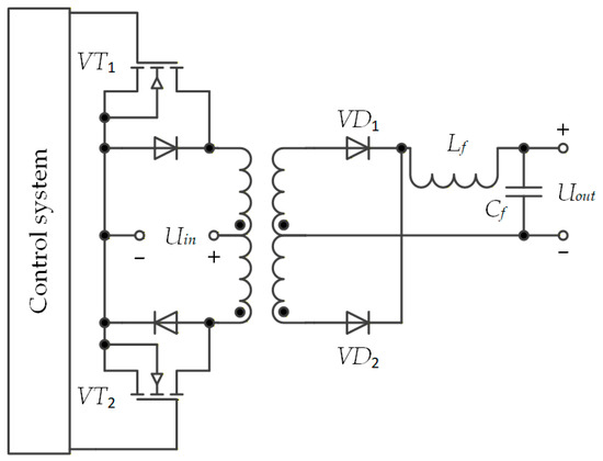
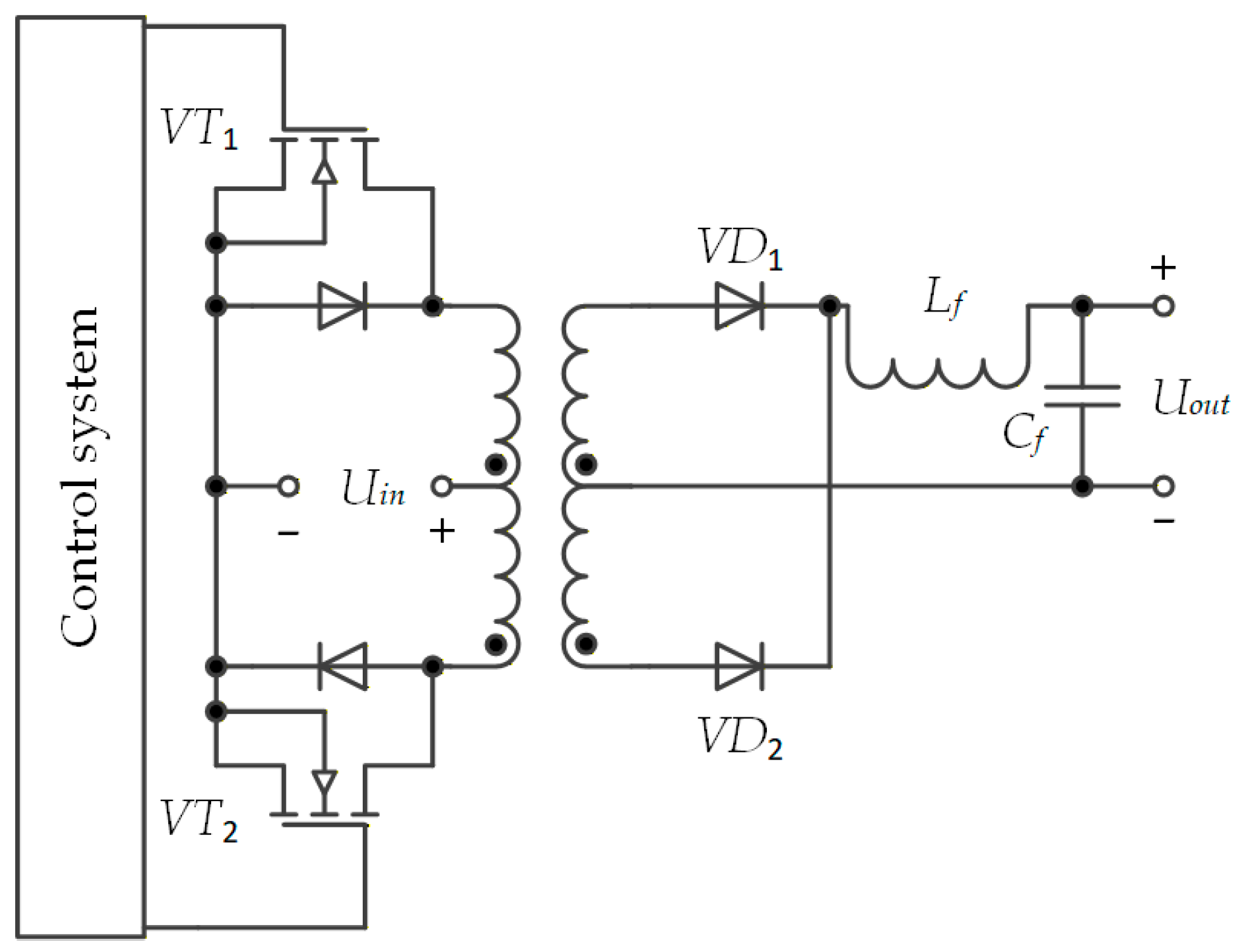
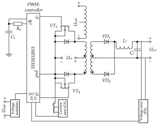
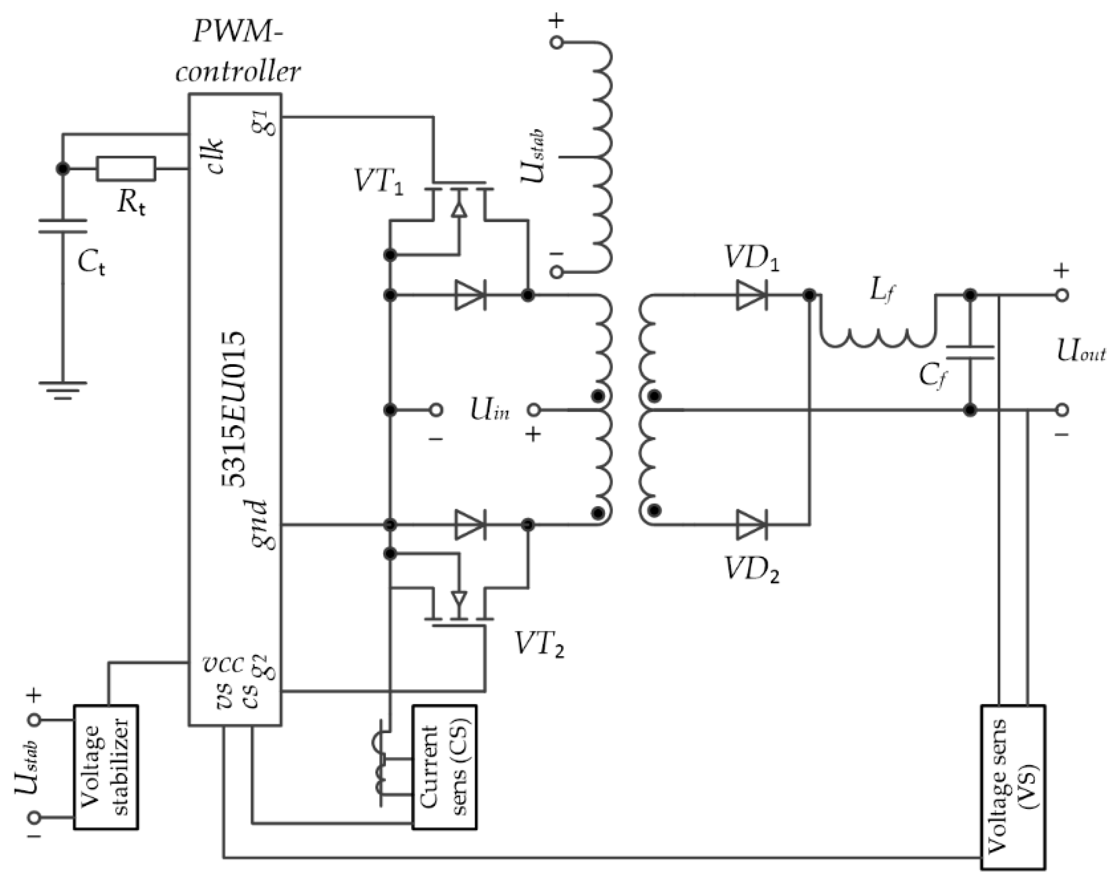
As a converter, based on the PWM controller 5315EU015, a push–pull converter circuit was proposed (a converter with the output of the transformer primary winding midpoint), Figure 1. The choice of this PWM controller was made taking into account its radiation resistance, clock frequency up to 500 kHz, low supply voltage of 5 V, and the presence of protections. The protections of this microcontroller include protection against overlapping control signals, short circuit protection, over-voltage protection, as well as when the supply voltage is low.
Figure 1.
Push–pull converter circuit with the output of the transformer primary winding midpoint.
The converter basic circuit based on 5315EU015, a single-channel version with 5 V is shown in Figure 1.
It is proposed to upgrade this circuit to a four-channel one with an input voltage 24 ± 1 V, a power 10 W, two output channels 5 ± 0.25 V and two channels 15 ± 0.75 V. The dimensions were specified at the design stage, but should not be taken into account in the experimental layout, it is 30 × 50 mm2, the height requirements depend on the field of application, but should not be less than 10 mm. Based on the technical specification, the voltage and current ripple is 5%, the minimum efficiency should not be lower than 90%. The switching frequency should be between 300 kHz and 500 kHz. There are no requirements for frequency response and frequency response at this stage. NTD18N06LT4G was selected as VT1 and VT2 transistors, also the remaining elements correspond to those proposed in the documentation for 5315EU015 [28,29].
3. Simulation
Using the method of differential equations algebraization (ADE) [12], a mathematical model of a push–pull converter was constructed with the midpoint output of the transformer primary winding. The mathematical method is based on the transformation of differential equations described by Kirchhoff’s laws into their algebraic form. Each variable of the differential equation is averaged over a period and multiplied by the sine and cosine. As a result, the active and reactive components of the variables effective values are obtained. Previously, converters without a transformer were considered in this method and the calculation was performed without taking into account the switching function. An extension of the method will be considered in this model with switching function. Ref. [12] only explains the essence of this method in the state space. Thus, an extension of the differential equations algebraization method in the state space for DC–DC converters, in particular with galvanic isolation, is given. It is possible to find the effective values of the converter currents and voltages using the obtained mathematical expressions.
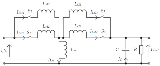
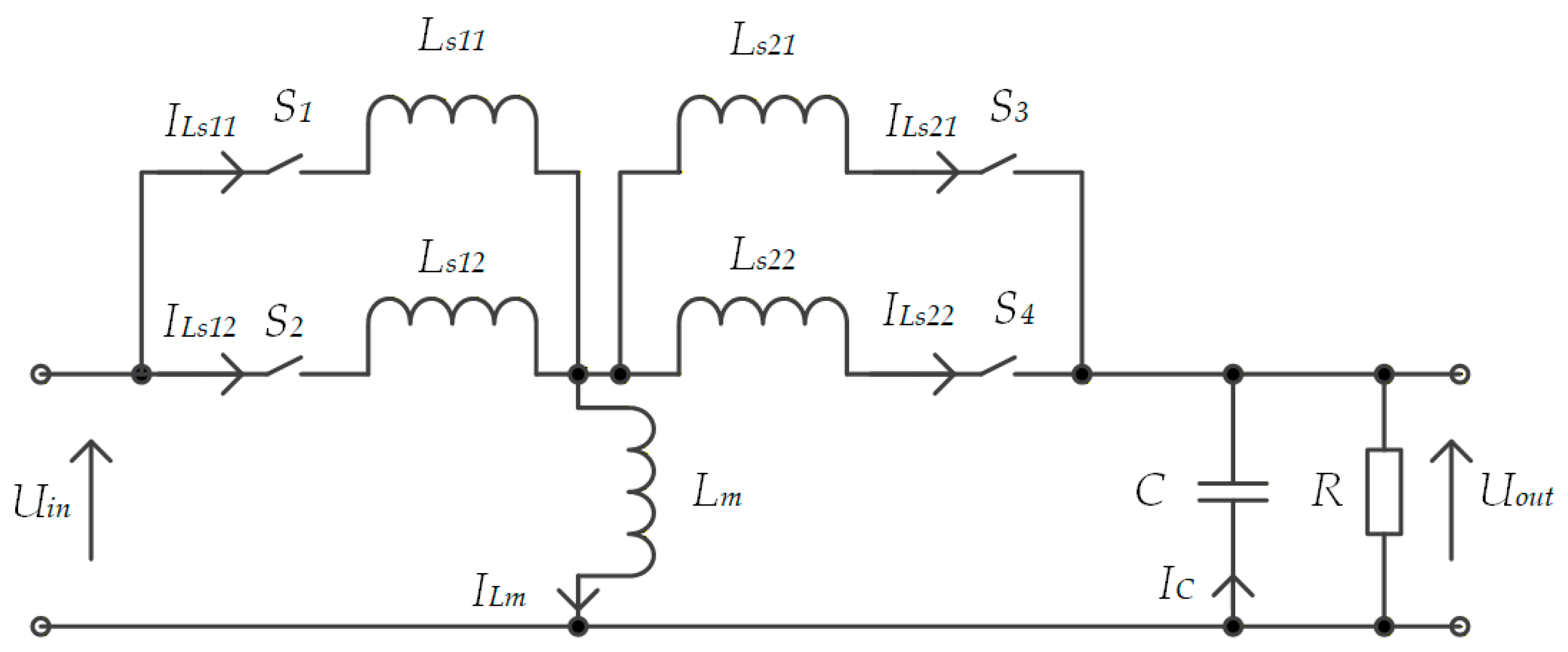
Figure 2 shows a scheme for replacing one channel of a push–pull converter.
Figure 2.
Push–pull converter replacement scheme.
Assumptions were made to build a mathematical model; thus, the winding resistances and the inductive filter were assumed to be zero. In order to take into account the operation of semiconductor switches when the S1S3 and S2S4 switches are closed, two versions of the equations systems are written, where ψ = 1 when S1S3 is switched on and ψ = 0 when S2S4 is switched on. Also, the switching function (1) takes two forms for the active components of the sine (2), and the reactive components of the cosine (3).
where M is the modulation depth, fh is the switching frequency, and T is the network period.
For the scheme in Figure 2, the system of equations when the S1S3 switches are switched on looks like this (4):
The system of equations when the S2S4 switches are switched on is as follows (5):
Each variable can be represented as their active and reactive components, orthogonal to each other. Further, after the algebraization procedure, we obtain a matrix of 12 equations connected by a switching function (6)–(9).
The expression consists of three parts, where matrix B is a matrix of coefficients (7), matrix A is a vector column of variables (8), and matrix C is a vector column of input sources (9).
To get the resulting value of each variable, perform (10):
Thus, to obtain the current value of the output voltage, Xy must be replaced with Uout. As a result, it is possible to obtain a control characteristic. This is because in the coefficients matrix there is a switching function in which the modulation depth (or pulse duty cycle) is included. The obtained data can also be used to verify the data obtained in the simulation of the PSIM program, which will be discussed later.
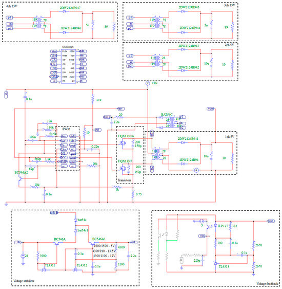
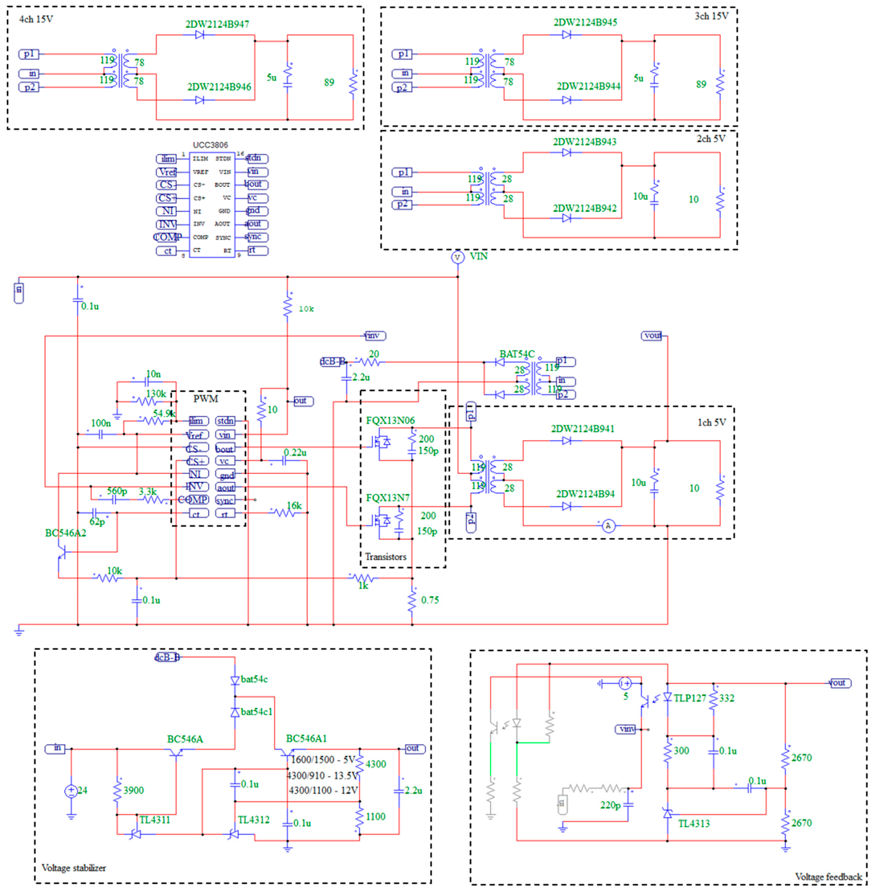
A close analog of 5315EU015 PWM controller is UCC3806 (UC3846). A model was realized in the PSIM software v. 22.2, where there is a model of this microcircuit; Figure 3 and Figure 4 [30,31,32].
Figure 3.
An example of a scheme for using the 5315EU015 microcircuit in a secondary power supply from an on–board network 27 V at a voltage 5 V with a power 10 W.
Figure 4.
Schematic diagram of a 10 W secondary voltage source based on UCC3806.
3.1. Equivalent Transformer Replacement Circuit
During the simulation, the following notes were identified:
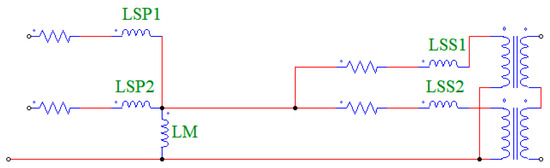
The transformation coefficients were determined in an open–loop system, and the transformer was modeled as a parallel connection of for five transformers with two primary and two secondary windings. Due to the fact that the replacement circuit for this type of transformer operates erratically in the PSIM software v. 22.2, the following model was considered as a replacement circuit, Figure 5.
Figure 5.
Transformer replacement circuit.
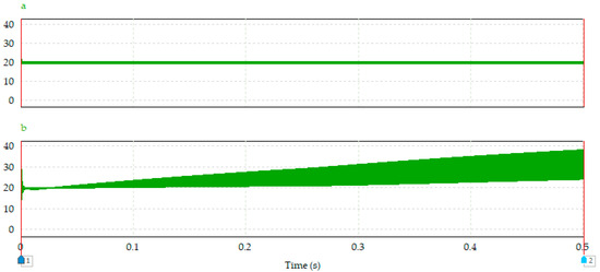
An example of transformer operation is shown in Figure 6.
Figure 6.
An example of the transformer replacement circuit with a split winding operation: ((a)—the required voltage form; (b)—the form in the model).
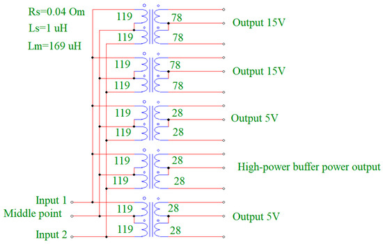
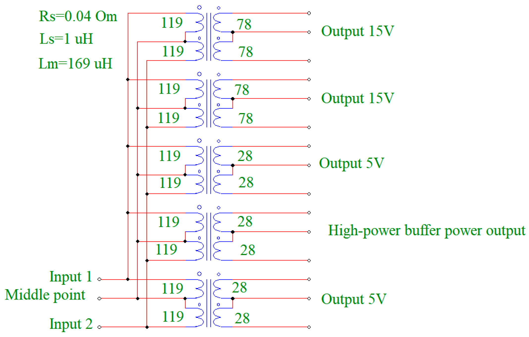
This model construction option in the PSIM software v. 22.2 turned out to be unsatisfactory because the output voltage significantly exceeded the required value during the transient process and did not reach steady state. This behavior is probably due to unsuitable transformer models, which are shown in the figure on the right. In this regard, a multi–winding transformer with two primary windings and ten secondary windings (eight for output channels and two for power of a powerful MOSFET buffer) was obtained through a parallel connection of five transformers, Figure 7.
Figure 7.
A multi–winding transformer of a simulation model with two primary windings and ten secondary windings.
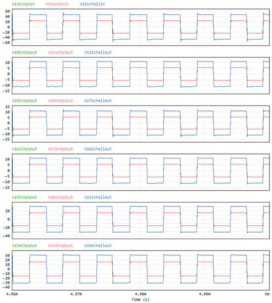
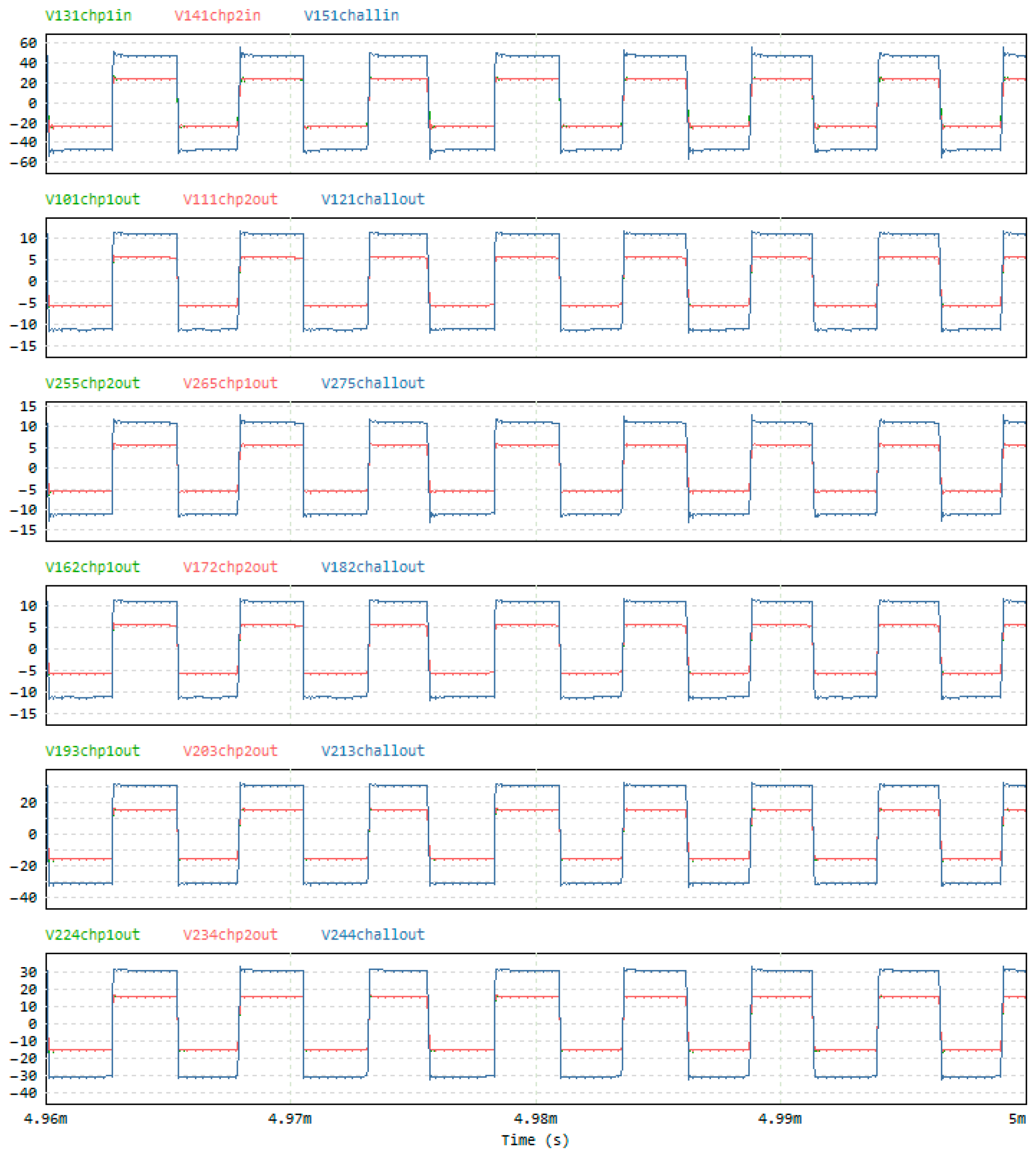
The parameters of the researched transformer were taken from the article [33] because it is planned to manufacture a planar transformer. There, the resistance ratings of the primary and secondary windings are measured and equal to 0.47 Ω, the scattering inductance is 0.249 µH and the magnetization inductance is 10.1 µH. Nevertheless, these parameters were significantly modified during modeling, and the following resistance equal to 0.04 Ω, scattering inductance equal to 1 µH, and magnetization inductance equal to 169 µH are recommended. Such requirements were obtained from the manufacturer of the JSC Scientific and Production Enterprise “Optical and Electronic complexes and Systems” transformer. The ratio of turns for the 5 V channel was 119/28, the ratio of turns for the 15 V channel was 119/78, the ratio of turns for power of a powerful buffer channel was no more than 119/28 (where 119 turns are on the primary side of the transformer, and 28 and 78 on the secondary, respectively). The voltage of the primary and secondary windings (order: primary, secondary winding of the first channel at 5 V, secondary winding of the power of a powerful buffer channel, secondary winding of the second channel at 5 V, secondary winding of the first channel at 15 V, secondary winding of the second channel at 15 V) is shown in Figure 8 [34,35,36,37].
Figure 8.
Voltage of the transformer windings (three curves are presented in each graph, two correspond to the voltages of the half-windings, the third correspond to the voltage between the terminals of the two half–windings).
The amplitude and effective voltage values are shown in Table 1, which were obtained from the PSIM software v. 22.2.
Table 1.
Amplitude and effective values of the winding voltages (in the name V13, V14, V15—voltages on the high side of the transformer; V10, V11, V12—voltages on the low side of the transformer 5 V first channel; V25, V26, V27—voltages on the low side of the power of a powerful buffer channel; V16, V17, V18—voltages on the low side of the 5 V second channel; V19, V20, V21—voltages on the low side of the 15 V first channel; V22, V23, V24—voltages on the low side of the 15 V second channel; “e-03” means “×10−3”, etc.).
It can be seen that the voltage levels on the secondary windings of the transformer correspond to the declared ones according to the above data table. Thus, for the 15 V channel, the level was 15.4 V, which also corresponds under the technical specification and no more than 15.7 V. For the 5 V channel, these data were 5.5 V, there is an overestimated value here, but it can be corrected due to the operation of the converter.
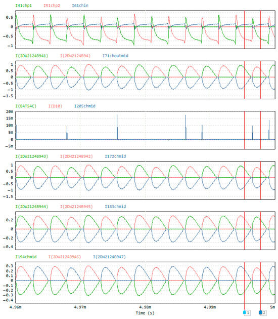
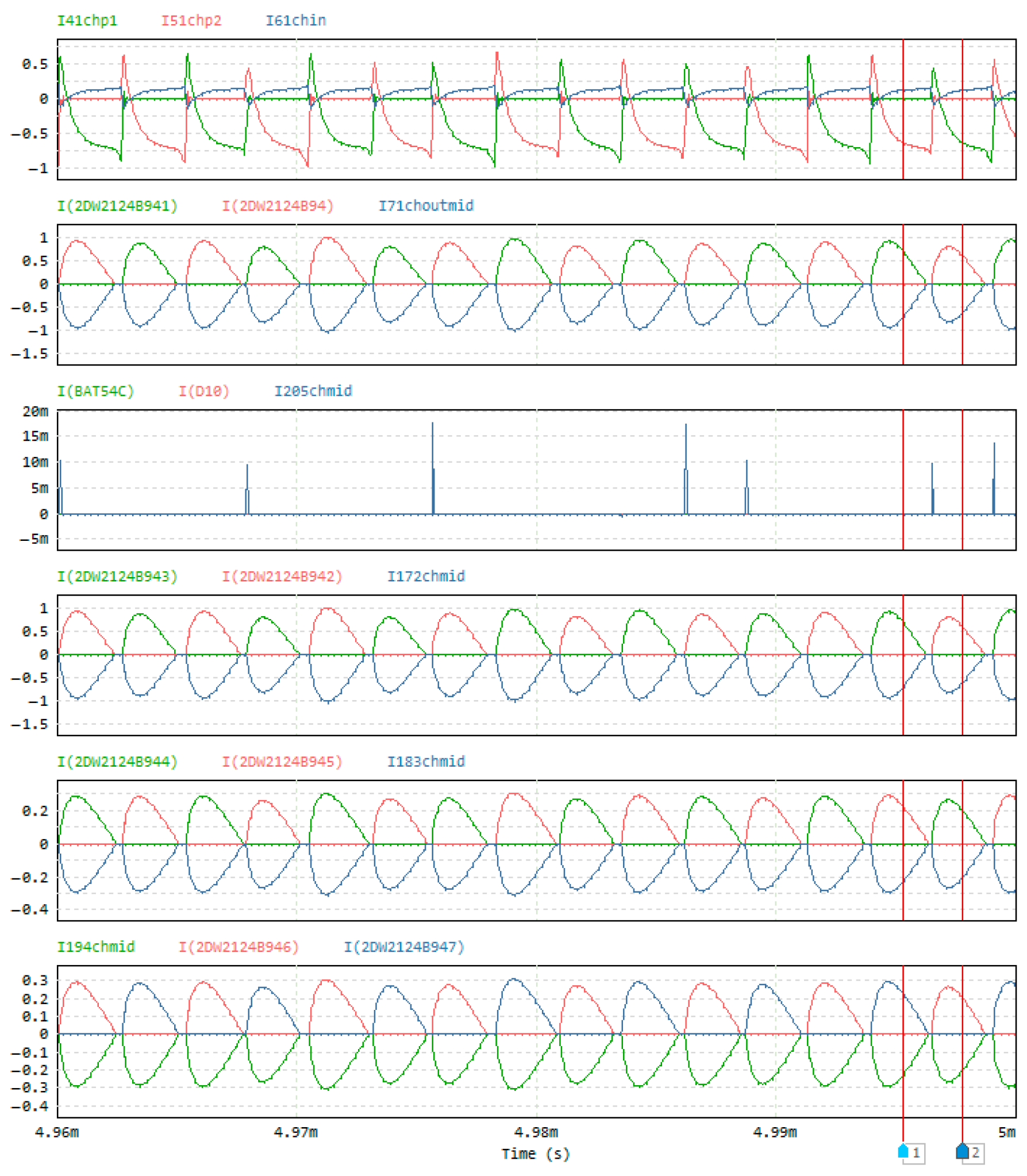
The currents of the primary and secondary windings (order: primary, secondary of the first channel at 5 V, secondary of the powerful buffer power channel, secondary of the second channel at 5 V, secondary of the first channel at 15 V, secondary of the second channel at 15 V) are shown in Figure 9.
Figure 9.
Currents of the primary and secondary windings (order as shown in Figure 8).
The maximum and minimum values are shown in Table 2, which were obtained from the PSIM software v. 22.2.
Table 2.
Maximum and minimum currents values of transformer (“e-01” means “×10−1”, etc.).
According to the oscillograms of the transformer currents and voltages, it can be concluded that they correspond to the predicted curves and such a transformer can be used in this model. In turn, the winding currents do not exceed the set values, 2 A. Also, the distribution of currents across the windings is symmetrical, which indicates uniform loading of the transformer.
3.2. An Analog of the 5315EU015 Microcircuit
Some pins of the UCC3806 microcircuit correspond (are similar, perform the same function) to the pins of 5315EU015, Table 3.
Table 3.
Correspondence of the UCC3806 microcircuit pins to the 5315EU015 pins.
There are outputs similar in functionality, presented in Table 4.
Table 4.
Correspondence of the UCC3806 microcircuit terminals with terminals of the 5315EU015 similar in functionality.
3.3. Analogs of Related Circuit Elements
The selection of the power unit elements was carried out in accordance with the technical specification for the secondary power supply. In particular, the output power and voltage of the converter were known. The calculation of the filter inductor Lf, Figure 3, was performed according to the Formula (11) [20].
where Uout is selected from the output voltage level of 5 V or 15 V, the output current Iout is determined from the set output power 2.5 W per channel, the switching frequency fs is taken from the technical specification and is equal to no more than 500 kHz. The fill factor γ is taken as a value close to 0.5 because only at this level is it possible to achieve the required output voltage values with a PWM controller 5315EU015. In this regard, for the 5 V channel, the output inductance was 5 µH, and for the 15 V channel it was 15 µH. For a 5 V channel, the most suitable inductor turned out to be VLS3015CX-4R7M-1, the value of the inductance to be less than calculated, but according to the experimental results, this value became to be acceptable, since the current is additionally smoothed due to the inductance of the transformer. The VLS3012HBX-150M choke was suitable for the 15 V channel.
The calculation of the filter capacitor Cf, Figure 3, was performed using the Formula (12).
where Ioutmax was 0.525 A and Ioutmin was 0.475 A based on the technical specification for the 5 V channel and 0.178 A with 0.162 A for the 15 V channel, respectively. The range of the discharge voltage should not exceed 0.0001 V, and therefore the capacity of the filter capacitor was 12 µF for the 5 V channel and 1 µF for the 15 V channel. Capacitors JCK1C100M040054 for the 5 V channel and JCK1H4R7M040054 for the 15 V channel were selected with a margin.
The choice of semiconductor elements was made based on design features, forward current, reverse voltage and switching frequency. The reverse voltage was determined according to the Formula (13), and the forward current according to the Formula (14).
where the reverse voltage on the diode was 20 V for the 5 V channel, and 60 V for the 15 V channel. The forward current, respectively, was 0.279 A for the 5 V channel and 0.1 A for the 15 V channel. Diodes with a margin of 80SQ045 were selected. The power transistors were selected based on the input voltage of the converter, at least 24 V and the input current, at least 0.5 A. The transistors were also selected with a margin is NTD18N06LT4G. The delivery time of the items was also taken into account when selecting the elements.
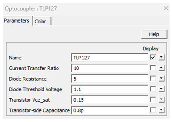
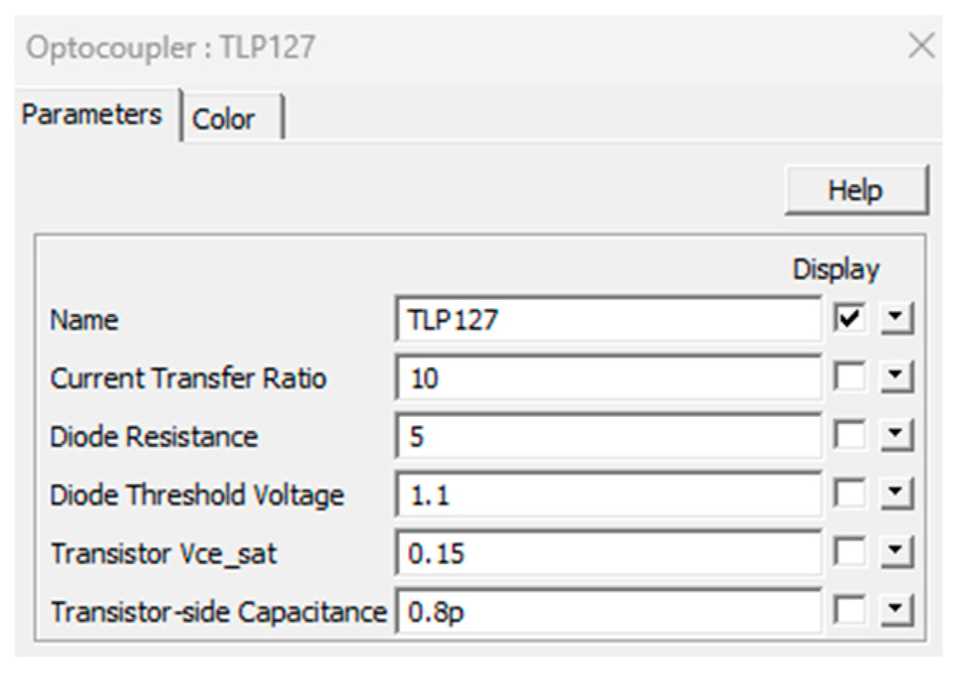
When modeling the “reverse voltage circuit”, Figure 4, the TLP127 optocoupler does not work with the parameters from the documentation for this chip, and therefore its standard parameters from PSIM were used, Figure 10. The orders of the input values magnitude were probably not observed in the PSIM software v. 22.2, and therefore these data can be considered correct, adjusted by an order of magnitude from the documentation.
Figure 10.
Parameters of the TLP127 optocoupler.
The parameters of the voltage stabilizer for the 5315EU015 are different from its analog. Due to the fact that different levels of the controller power supply, in turn, the power level of the powerful transistor buffer also changes, for the UCC3806 it is at least 10 V as well as in the model 12 V, which meets the requirements of the NTD18N06LT4G transistor. For 5315EU015, the use of such a transistor is allowed, but requires experimental verification, since the documentation does not specify the edge times at Vgs = 5 V, an alternative option is RFD16N06LESM.
The calculation of the RC circuit for setting of the internal clock generator frequency was performed according to the Formula (15).
The parameters R = 28 kΩ, C = 100 pF corresponds to the frequency 500 kHz.
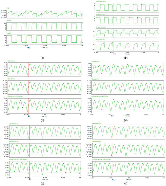
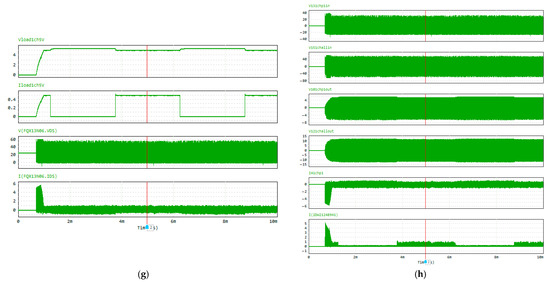
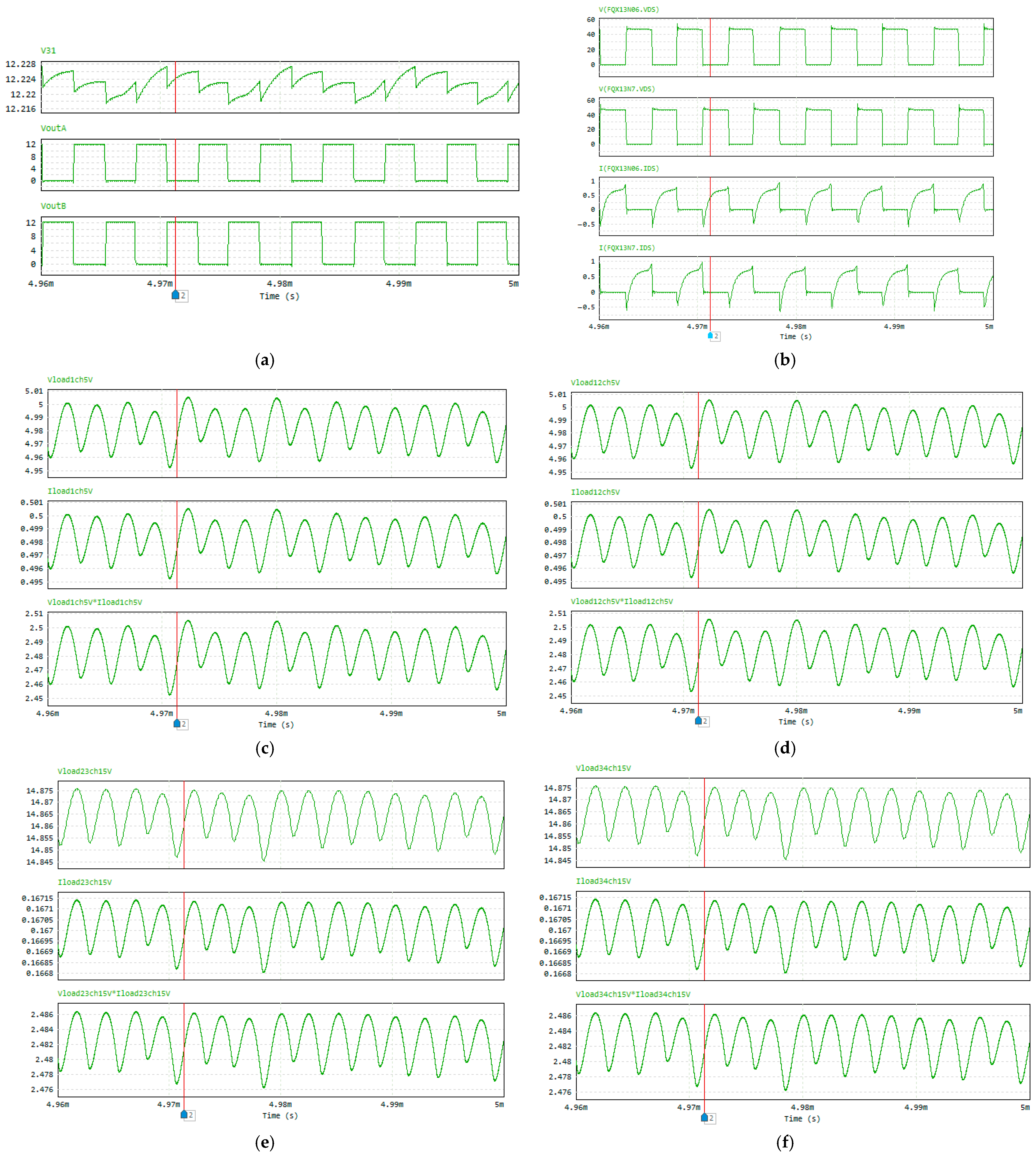
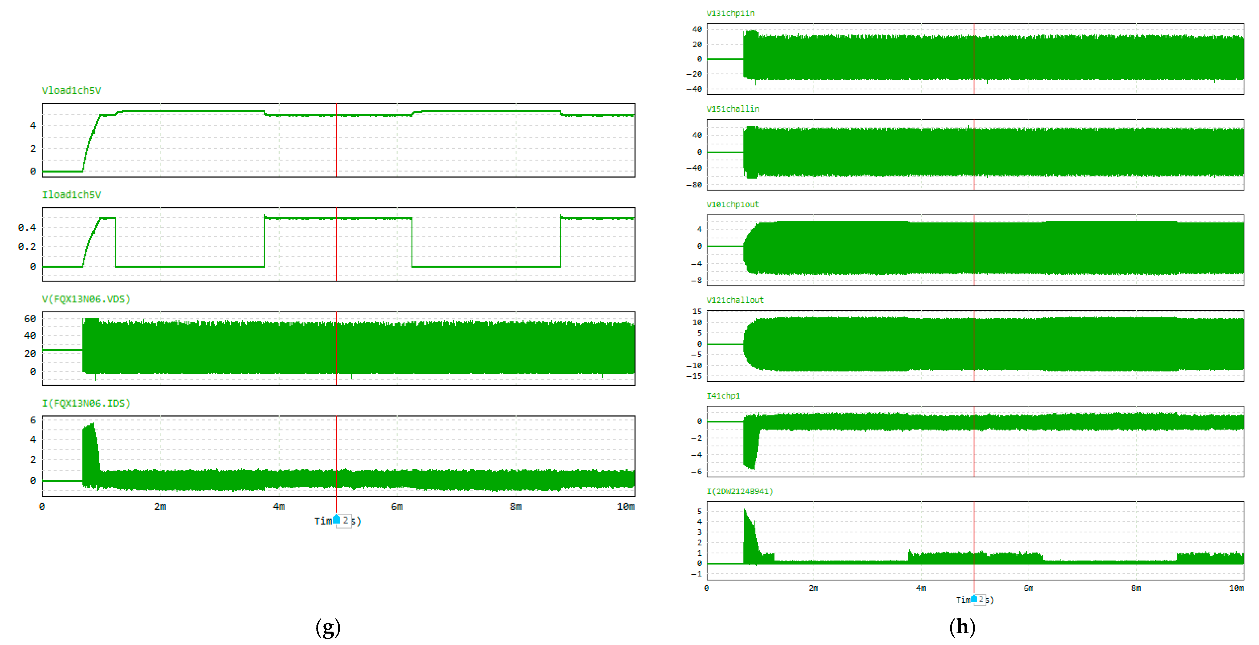
The simulation results of the circuit main nodes are shown in Figure 11.
Figure 11.
Simulation results (a) voltages on the power of a powerful buffer, top and bottom transistor control pulse, (b) voltage and current of top and bottom arm transistors, (c) voltage, current, and power of 5 V channel 1, (d) voltage, current, and power of 5 V channel 2, (e) voltage, current, and power of 15 V channel 1, (f) voltage, current, and power of 15 V channel 2, (g) transients (voltage and current of 5 V channel 1, voltage and current of the power transistor), (h) transients (voltage of primary winding and secondary winding 1–4 graphics, current of primary winding and secondary winding 5–6 graphics)).
Recommendations for choosing a transformer, a voltage stabilizer configuration, and a feedback circuit were identified during the development of a secondary power supply based on 5315EU015. At the moment, the requirements for choosing a power transistor are concluded, in particular, for choosing the supply voltage level of the switch, the following options are proposed: RFD16N06LESM, GAN7R0-150LBE, RJF0613JSP, RJF0619JPE, RJF0611JPE, RJF0606JPE, RJF0618JPE, RJF0619JPD, RJF0605JPD.
Based on the above waveforms, it can be concluded that the proposed converter model produces the required output voltage levels and the power of each channel is within 2.5 W, which in total results in 10 W of load power specified in the technical specification.
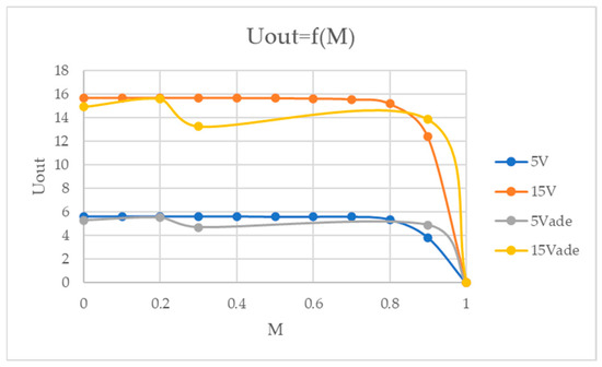
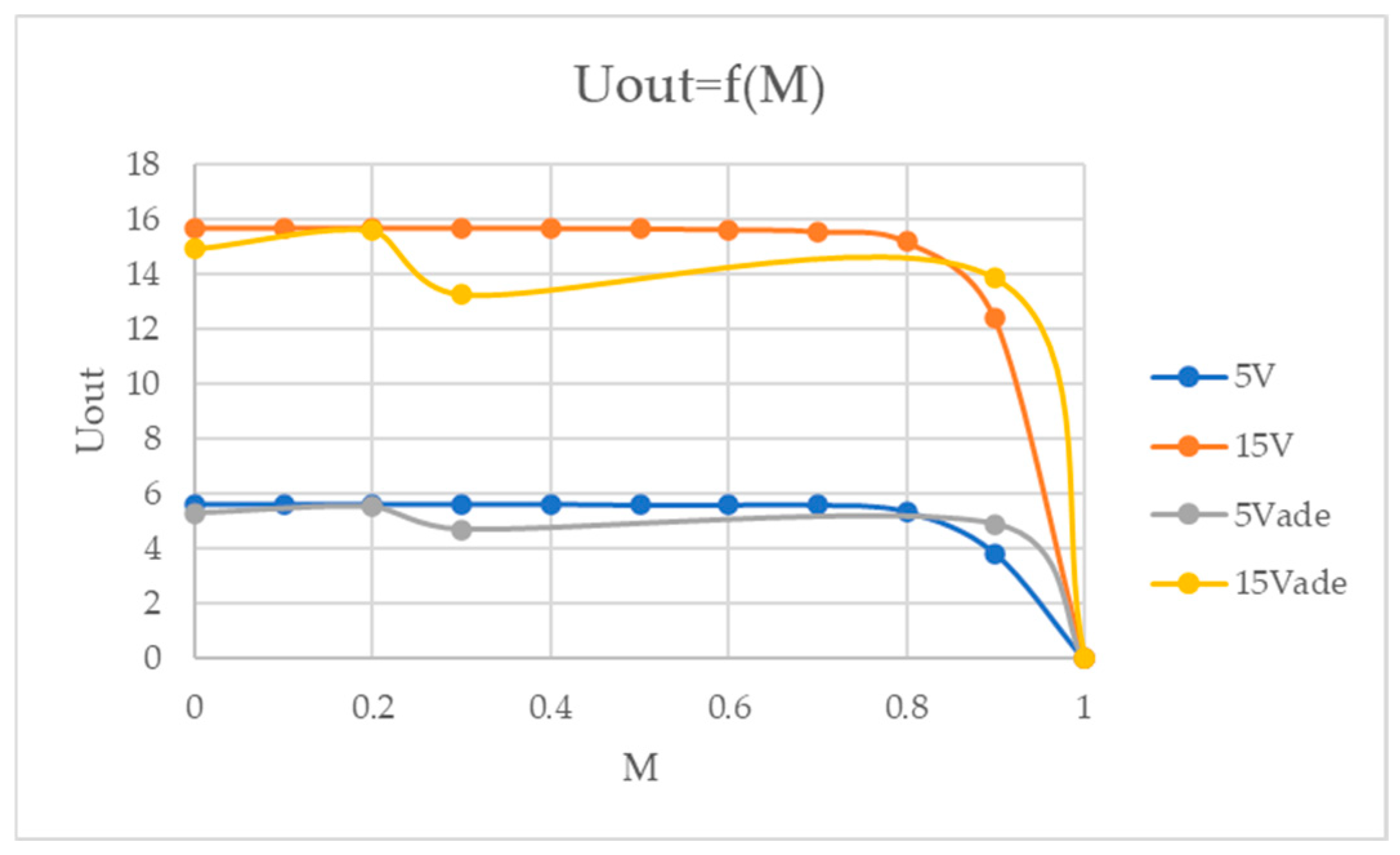
Also, the results of modeling the mathematical model, a control characteristic was constructed, Figure 12. The characteristic is constructed for the open loop, in turn, it can be seen that the operating range of the modulation depth M varies from 0.8 to 0.9, where the required voltage levels of 5 V and 15 V channels are formed. The figure shows a comparison of the mathematical model obtained by the algebraization of differential equations (ADE) and in the PSIM program. It can be seen that there are fluctuations, in channel 15 V, which can be explained by the assumptions introduced into the model. Further improvement of the model will make it possible to obtain expressions for currents and voltages expressed in terms of the converter elements R, L, C the parameters.
Figure 12.
Control characteristics of a push–pull converter for 5 V and 15 V load channels.
4. Experiment
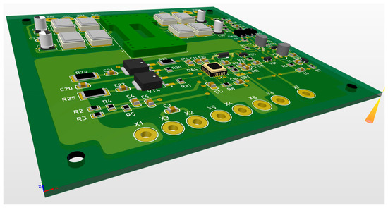
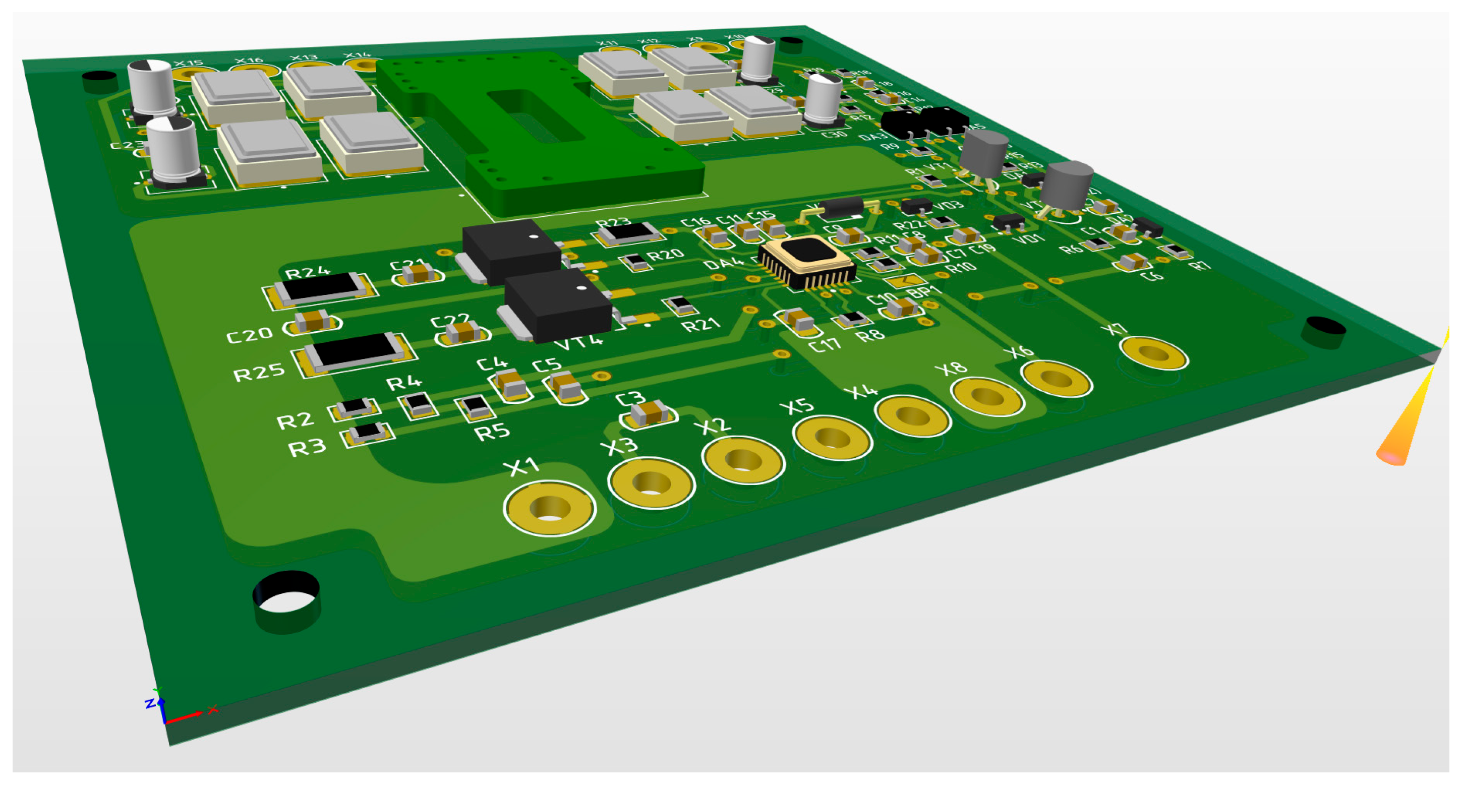
A schematic electrical diagram and printed circuit board were developed in the Altium Designer CAD, Figure 13, to verify and compare the operating modes of the secondary power supply with the mathematical model obtained in the PSIM. The calculation and selection of elements is performed in the Section 3.3.
Figure 13.
Printed circuit board of a four-channel power supply based on 5315EU015.
The nominal values of the elements used in the experiment are shown in Table 5.
Table 5.
Nominal values of the key scheme elements.
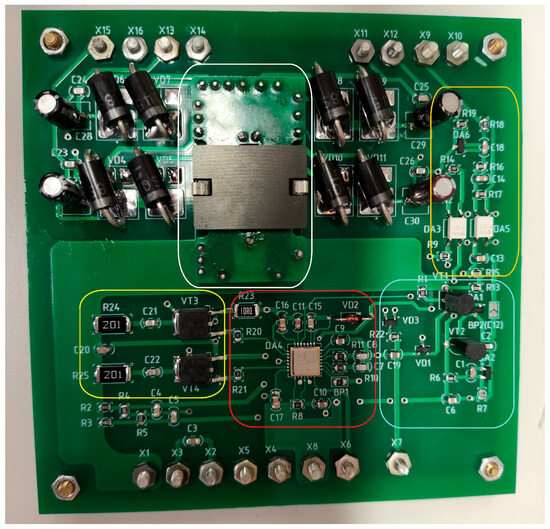
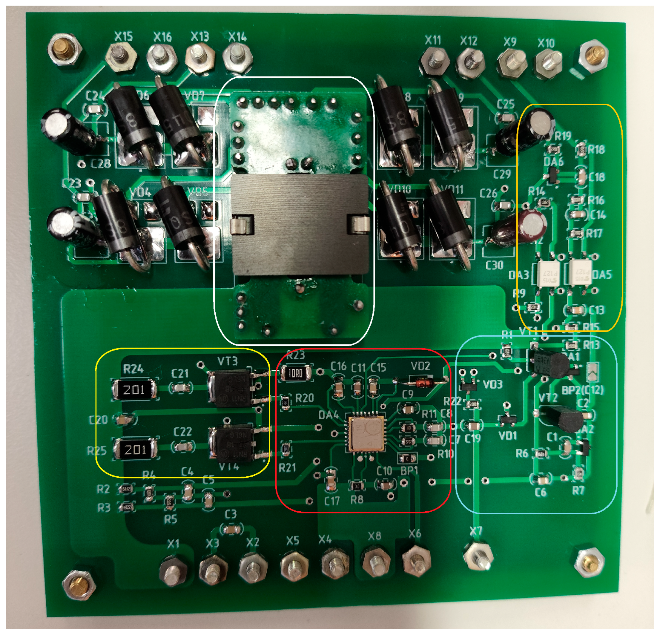
Figure 14 shows the assembled converter layout.
Figure 14.
Secondary power supply (white—TP22-6/2/2/2/4/4 planar transformer, red—5315EU015 PWM controller unit with elements, yellow—MOSFET transistor converter, blue—voltage stabilization unit, orange—feedback unit, X1,X2—24 V input, X4–X6—5 V input of the PWM controller resolution, X9,X10—5 V 1 channel output, X11,X12—5 V 2 channel output, X13,X14—15 V 3 channel output, X15,X16—15 V 4 channel output).
During the experiment, the following tasks were set:
- (1)
- Measurement of the clock frequency at the PWM controller OSCOUT pin.
- (2)
- Measurement of the duty cycle control voltage of the output signals at the PWM controller SLOPE pin in idle mode and under load.
- (3)
- Stabilization voltage measurement of the voltage stabilizer.
- (4)
- Measurement of the power supply voltage of the powerful buffer at the PWM controller VCCQ output.
- (5)
- Measurement of the VT1 and VT2 transistors control pulses in idle mode and under load at terminals Q and QB, respectively.
- (6)
- Measurement of the secondary power supply four channels output voltage in idle mode and under load.
- (7)
- Measurement of the secondary power supply four channels output currents.
The tests were carried out at a supply voltage 24 ± 1 V and a load power up to 10 watts. Test procedure: apply a 24 V supply voltage to the input of the secondary power supply and perform measurements in idle mode and under load. The load uses resistances with a power of at least 2 watts and ratings of 10 Ω for 5 V channels and 90 Ω for 15 V channels.
The list of used test equipment is given in Table 6.
Table 6.
List of used measuring equipment.
4.1. Measurement of Static Parameters in Idle Mode
The results of potentials measurements in idle mode are shown in Table 7.
Table 7.
Measured values of the secondary power supply nodes potentials in the idle mode.
The results of potential measurement at rated load are shown in Table 8.
Table 8.
Measured values of secondary power supply nodes potentials under load.
It is worth noting that during the experiment, the efficiency of the converter was more than 90%, which satisfies the technical specification, namely 95. Current and voltage ripples did not exceed 5%.
The results of comparing outside manufacturers’ multichannel converters with the proposed converter are shown in Table 9.
Table 9.
Comparison of multi-channel radiation-resistant converters.
The proposed converter based on the PWM controller 5315EU015 is a non–serial product, but only a prototype. In this regard, it is not entirely correct to compare it with mass–produced products; however, some parameters can be evaluated. Galvanically isolated converters are used everywhere, with a switching frequency of up to 500 kHz. The efficiency of such devices is estimated to be up to 90%, and the power is from 10 to 50 W, which indicates the competitiveness of the proposed converter. The accuracy of the output voltage can be further increased, but there were no such requirements in the technical specification. But unlike competitors, the converter based on the 5315EU015 PWM controller has the largest number of protections, not only short circuit and overvoltage protection, as with competitors, but also protection against overlapping control signals, as well as when the supply voltage is low. This is an advantage over competitors.
4.2. Measurement of Dynamic Parameters
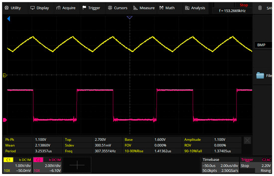
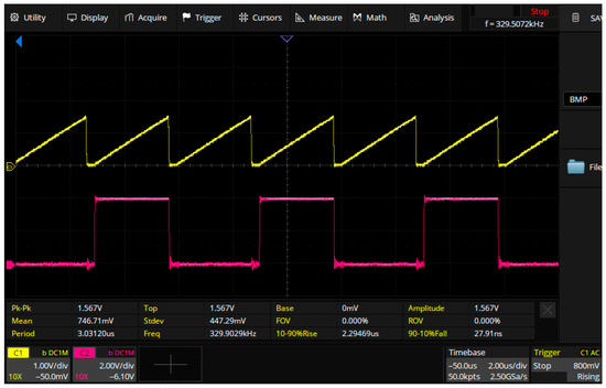
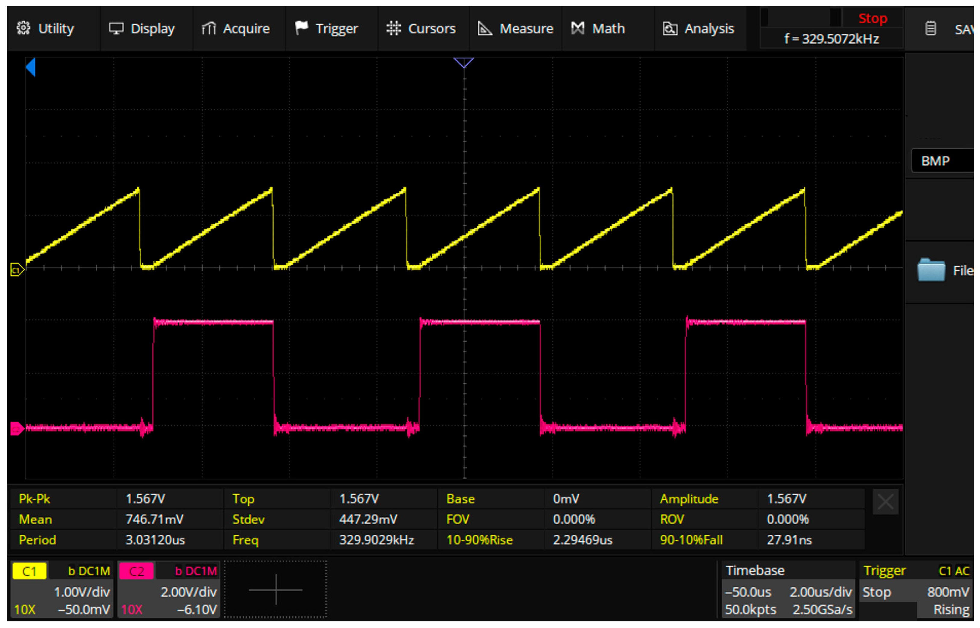
The voltage waveform at the OSCOUT pin is shown in Figure 15. The signal frequency at the OSCOUT pin during the calculation should have been 500 kHz. The calculation formula is given in the PWM controller documentation, a capacitor 100 pF and a resistance of 27 kΩ were installed in the circuit, which, according to the expression 1.4/RC, gives 518 kHz. The frequency reached 303 kHz according to the results of the experiment. It is proposed to correct the RC circuit by 27 kΩ and 150 pF.
Figure 15.
Voltage waveform at the OSCOUT pin.
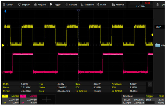
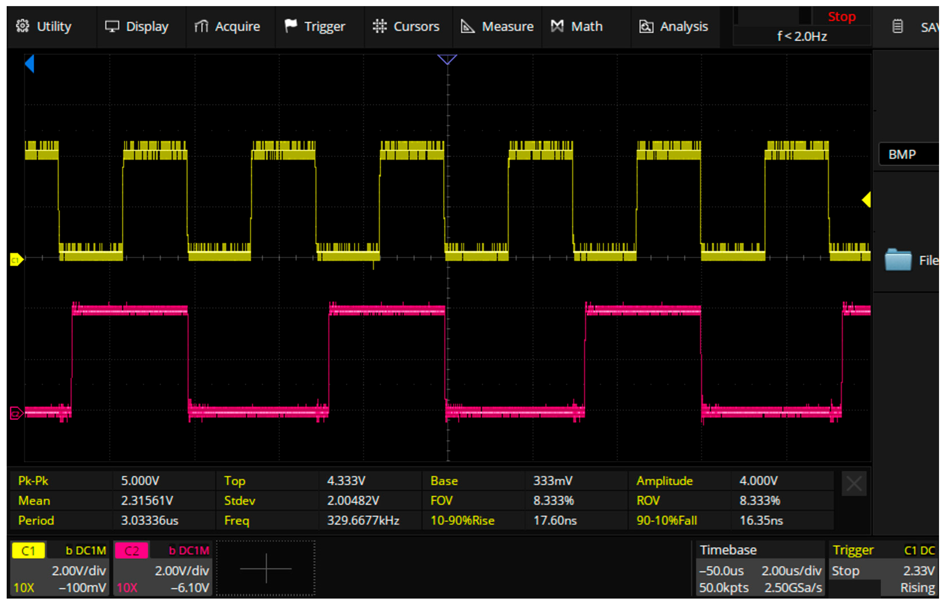
The RC circuit input of the clock generator and the switches control pulses are also compared, Figure 16.
Figure 16.
Voltage waveform at the Q terminal together with the RC input of the clock generator circuit.
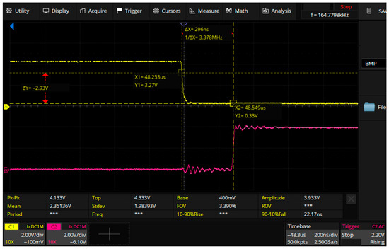
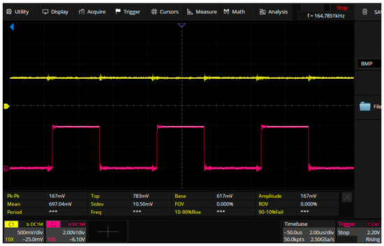
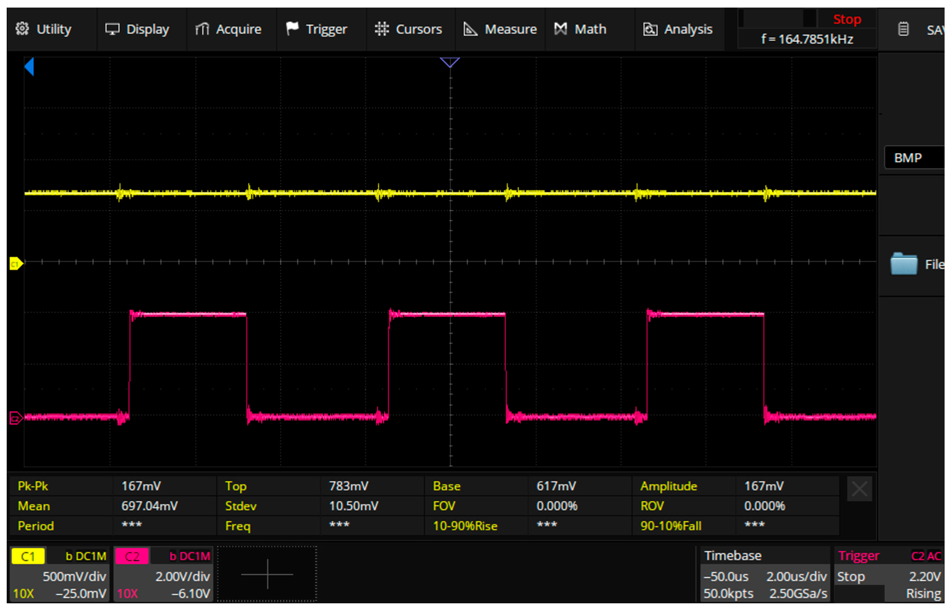
Figure 17 shows a comparison of the control pulses on the switch’s gates.
Figure 17.
Dead time between switches pulses, 296 ns (*** this means that the value cannot be measured).
The voltage waveform at the SLOPE pin is shown in Figure 18. The signal is generated through an RC circuit connected to the supply voltage, which corresponds to the maximum possible duty cycle. If there is feedback, this level is lower, and therefore the output voltage does not meet the norm. It was decided to refuse feedback and install linear stabilizers.
Figure 18.
Voltage waveform at the SLOPE pin.
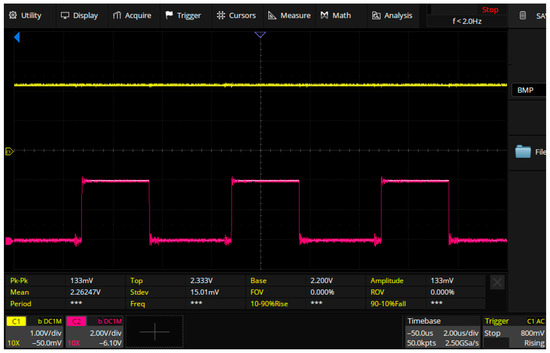
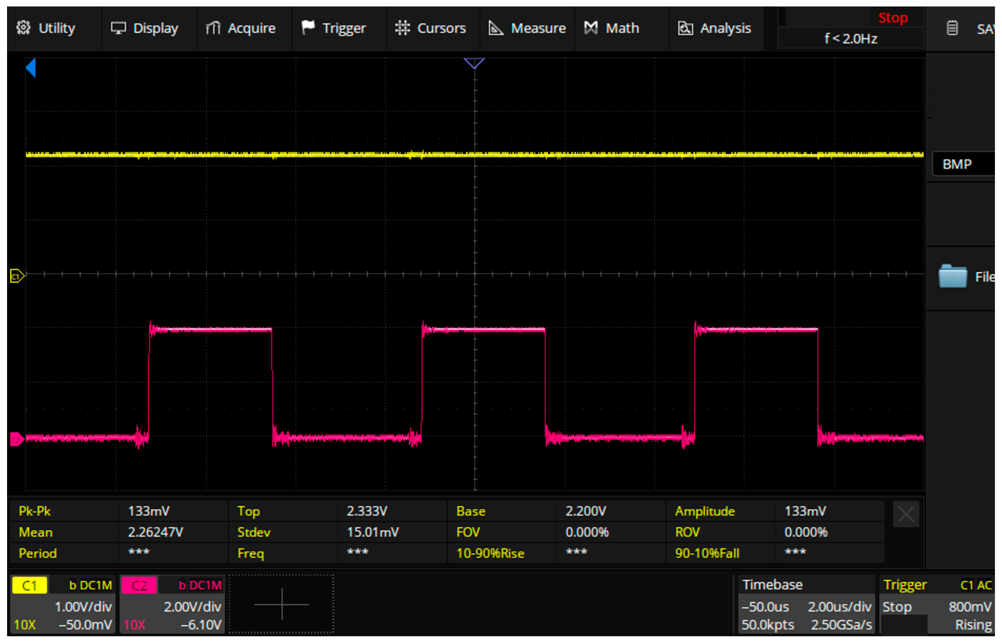
The waveform of the signals on the protection terminals, OVER, and the input of the supply voltage indicator above the norm is also given. When the recommended voltage is exceeded, the protection is activated, Figure 19. The input of the short circuit protection (short circuit) indicator, at a low level, indicates that the protection has been activated, Figure 20.
Figure 19.
Input of the above–normal supply voltage indicator (*** this means that the value cannot be measured).
Figure 20.
Input of the short circuit protection feature (*** this means that the value cannot be measured).
5. Conclusions
During the development of a secondary power supply based on 5315EU015, a mathematical model of a push–pull converter was built. Based on the simulation results, the operating range affecting the fill factor of the transistor control pulses was determined. Recommendations for designing a transformer, configuration of a voltage stabilizer, and a feedback circuit were identified.
The model of the transformer has also been corrected to achieve a more stable output voltage level of the secondary winding. Due to the fact that dimensions are important for this type of converter, a planar version of the transformer was chosen. The manufacturer of this transformer has already made changes to the number of primary and secondary winding turns. So, for the primary winding, the number of turns was six turns, for the secondary winding of the 5 V channel two turns, and for the secondary winding of the 15 V four turns. The conversion coefficient of the 5 V channel turned out to be lower, but due to the fact that the operating range on the control characteristic was not at the boundary, it was possible to lower the output voltage of the 5 V channel by changing the fill factor (borehole) of the control pulse.
The signal frequency at the OSCOUT pin during the calculation should have been 500 kHz. The calculation formula is given in the PWM controller documentation, where a capacitor 100 pF and a resistance of 27 kΩ were installed in the circuit, which, according to the expression 1.4/RC, gives 518 kHz. According to the results of the experiment, the frequency reached 303 kHz. It is proposed to correct the RC circuit by 27 kΩ and 150 pF.
The voltage values at the first output channel in the idle mode were 5 V, which corresponds to the technical specification. In turn, feedback was disabled, which affected to the width of the control pulses. The voltage value of the second channel was also 5 V. The voltage of the third and fouth channels, in turn, corresponds to the technical specification 15 V.
The voltage level of the VCC and VCCQ terminals are at the maximum allowable level, with 4.2 at the required 4.5. Nevertheless, the PWM controller is functioning, and it is necessary to correct the level of the stabilized voltage in the stabilization circuit.
The output voltage of the secondary power supply is 4.9 V on the first and second channels and 15 V on the third and fourth channels under load.
Further development involves the creation of a hybrid model, where shell-less elements will be used.
Author Contributions
Conceptualization, A.U.; methodology, A.U. and P.S.; software, A.U. and P.S.; validation, D.S.; formal analysis, A.U.; investigation, A.U., P.S. and D.S.; resources, A.U. and P.S.; data curation, A.U.; writing—original draft preparation, A.U.; writing—review and editing, A.U.; visualization, A.U.; supervision, D.S.; project administration, A.U. All authors have read and agreed to the published version of the manuscript.
Funding
This research received no external funding.
Institutional Review Board Statement
Not applicable.
Informed Consent Statement
Not applicable.
Data Availability Statement
The data presented in this study are available on request from the corresponding author. The data are not publicly available due to privacy issues.
Conflicts of Interest
The authors declare no conflicts of interest.
References
- Babaiahgari, B.; Valdez-Resendiz, J.E.; Alejo-Reyes, A.; Rosas-Caro, J.C.; Silva-Vera, E.D. Quadratic Boost Converter with Reduced Input Current Ripple. Appl. Sci. 2025, 15, 10815. [Google Scholar] [CrossRef] [Scilit]
- Wu, T.F.; Chen, Y.K. Synthesis of Multistage and Multilevel Converters; Wiley Semiconductors: Hoboken, NJ, USA, 2020; Available online: https://ieeexplore.ieee.org/abstract/document/10524622/ (accessed on 3 September 2025).
- Shukir, S.S. Buck, Boost, and Buck–Boost Converters Analysis: A. Available online: https://www.researchgate.net/profile/Samhar-Shukir/publication/396271523_Buck_Boost_and_Buck-Boost_Converters_Analysis_A_Review/links/68e5303dd221a404b2a60de7/Buck-Boost-and-Buck-Boost-Converters-Analysis-A-Review.pdf (accessed on 3 September 2025).
- Calabrese, D.; Tricarico, G.; Brescia, E.; Cascella, G.L.; Monopoli, V.G.; Cupertino, F. Variable structure control of a small ducted wind turbine in the whole wind speed range using a Luenberger observer. Energies 2020, 13, 4647. [Google Scholar] [CrossRef] [Scilit]
- Dizangian, N.; Jovanovic, S.; Poure, P. Modeling and Experimental Verification of a Single-Switch Quadratic Boost DC–DC Converter with High Voltage Gain for Energy Harvesting. Energies 2025, 18, 5447. [Google Scholar] [CrossRef] [Scilit]
- Singh, A.; Bharti, K.; Kumar, N. Comparative study between DC-DC buck converter and Zero Voltage switching buck converter. In 2024 IEEE International Students’ Conference on Electrical, Electronics and Computer Science (SCEECS); IEEE: New York, NY, USA, 2024; pp. 1–6. Available online: https://ieeexplore.ieee.org/document/10482318 (accessed on 3 September 2025).
- Permana, G.S. Pengaruh Perubahan Kapasitor Terhadap Kinerja Buck-Boost Converter. EEICT (Electr. Electron. Instrum. Control. Telecommun.) 2025, 8, 7–13. [Google Scholar] [CrossRef] [Scilit]
- Brescia, E.; Savastio, L.P.; Di Nardo, M.; Cascella, G.L.; Cupertino, F. Parameter Estimation of PMSMs Without Signal Injection and Dedicated Tests Considering Voltage Errors and Parameter Variations. IEEE Trans. Power Electron. 2025, 41, 2040–2056. [Google Scholar] [CrossRef] [Scilit]
- Guo, R.; Gao, H.; Chen, L.; Zhang, Y.; Wang, L. Lightweight, High-Efficiency, High-Dynamic-Response and Low-Ripple DC-DC Converters Based on Interleaved Magnetic Integrated Switched-Coupled Inductor for Electric Propulsion Aircraft. Aerospace 2025, 12, 1067. [Google Scholar] [CrossRef] [Scilit]
- Talebian, I.; Hosseini, S.H. A new DC-DC buck converter with soft-switching capability. In 2020 11th Power Electronics, Drive Systems, and Technologies Conference (PEDSTC); IEEE: New York, NY, USA, 2020; pp. 1–5. Available online: https://ieeexplore.ieee.org/abstract/document/9088440/ (accessed on 3 September 2025).
- Vasylenko, O.V.; Snizhnoi, G.V. Adaptive models of the four-switch buck-boost converter. Electr. Eng. Power Eng. 2025, 2, 49–58. [Google Scholar] [CrossRef] [Scilit]
- Zinoviev, G.S. Fundamentals of Power Electronics; Novosibirsk State University: Novosibirsk, Russia, 2004; Available online: https://elibrary.ru/item.asp?id=29973226 (accessed on 3 September 2025).
- Zhuravlev, A.A.; Mazel, K.B. DC Voltage Converters on Transistors; Energiya: Moscow, Russia, 1964. [Google Scholar]
- Petushkov, M.Y. DC Voltage Converters; Magnitogorsk State Technical University named after G.I. Nosov: Magnitogorsk, Russia, 2015; Available online: https://elibrary.ru/item.asp?id=30018470 (accessed on 3 September 2025).
- Acosta-Rodríguez, R.A.; Rosero-García, J.; Rivera, M.; Chaimanekorn, K. Recent Advances in Non-Isolated DC/DC Converter Topologies: A Review and Future Perspectives. Appl. Sci. 2025, 15, 12868. [Google Scholar] [CrossRef] [Scilit]
- Anuraag, B.V.; Mahalakshmi, R.; Likhtih, S.; Bhargavi, P.; Mohanty, A. Design and Comparative Study of DC-DC Quadratic Buck-Boost Converter and Cascaded Buck-Boost Converter. In 2021 International Conference on Recent Trends on Electronics, Information, Communication & Technology (RTEICT); IEEE: New York, NY, USA, 2021; pp. 642–646. Available online: https://ieeexplore.ieee.org/abstract/document/9573716/ (accessed on 3 September 2025).
- Pham, X.T.; Nguyen, M.T.; Pham, C.K.; Thuc, K.X. Buck Converter with Improved Efficiency and Wide Load Range Enabled by Negative Level Shifter and Low-Power Adaptive On-Time Controller. Electronics 2025, 14, 2425. [Google Scholar] [CrossRef] [Scilit]
- Mahdizadeh, S.; Sharivar, R.S.; Gholizadeh, H.; Afjei, E. A transformer less quadratic boost DC-DC converter with continuous input Current and a few number of components, based on Classical boost and cuk converter suitable for renewable applications. In 2021 29th Iranian Conference on Electrical Engineering (ICEE); IEEE: New York, NY, USA, 2021; pp. 252–257. Available online: https://ieeexplore.ieee.org/document/9544458 (accessed on 3 September 2025).
- Wang, D.; Xie, P.; Chang, M.; Hou, Z.; Li, N.; Wu, G.; Wang, X. The integrated interleaved Boost-LLC resonant converter ZVS enables conditional analysis. Circuit World 2025, 52, 31–41. [Google Scholar] [CrossRef] [Scilit]
- Geitenko, E.N. Secondary power supply sources. In Circuit Design and Calculation; Tutorial; SOLON PRESS: Moscow, Russia, 2008; Available online: https://elibrary.ru/item.asp?id=20243126 (accessed on 3 September 2025).
- Lalmalsawmi; Biswas, P.K. Full-Bridge DC-DC Converter and Boost DC-DC Converter with Resonant Circuit For Plug-in Hybrid Electric Vehicles. In 2022 International Conference on Intelligent Controller and Computing for Smart Power (ICICCSP); IEEE: New York, NY, USA, 2022; pp. 1–6. Available online: https://ieeexplore.ieee.org/document/9862426 (accessed on 3 September 2025).
- Mandal, S.; Prajof, P.; Adib, M. A Non-isolated Step-up DC-DC Converter Based on Modified Quadratic Boost and Cuk Converter. In 2024 IEEE International Conference on Power Electronics, Drives and Energy Systems (PEDES); IEEE: New York, NY, USA, 2024; pp. 1–6. Available online: https://ieeexplore.ieee.org/document/10961618 (accessed on 3 September 2025).
- Babazadeh, Y.; Sabahi, M.; Babaei, E.; Sun, K. Reliability Enhancement of Interleaved DC-DC Boost Converter. Iran. J. Sci. Technol. Trans. Electr. Eng. 2025, 49-4, 1–13. Available online: https://link.springer.com/article/10.1007/s40998-025-00939-7 (accessed on 20 December 2025). [CrossRef] [Scilit]
- Mustafin, I.F.; Kislitsin, P.N. DC/DC converters based on integrated circuits for defense and space purposes. Sci. Time 2015, 4, 505–511. [Google Scholar]
- Zhdankin, V. New Interpoint products: DC/DC converters for special applications. Power Electron. 2005, 5, 64–68. [Google Scholar]
- Zhdankin, V. Radiation-resistant hybrid-film DC/DC converters–standard components of SPACECRAFT power supply systems. Mod. Autom. Technol. 2012, 1, 26–41. [Google Scholar]
- Zhdankin, V. Highly efficient radiation-resistant DC/DC converters with low-voltage outputs are the optimal solution for modern digital loads. Compon. Technol. 2011, 10, 130–136. [Google Scholar]
- The Topology of the 5315EU015 Microcircuit. Available online: https://www.elibrary.ru/item.asp?id=39317472 (accessed on 14 January 2026).
- Description of the 5315EU015 Microcircuit. Available online: https://drive.google.com/file/d/1bRyjAj4SY3bb_yds04uxpD1nZkOuZRiw/view?usp=sharing (accessed on 10 February 2025).
- Yadav, J.G.; Yadav, Y.K.; Kumar, N. Mathematical modelling & simulation of synchronous buck converter and analysis of its simulation results. In 2023 International Conference on IoT, Communication and Automation Technology (ICICAT); IEEE: New York, NY, USA, 2023; pp. 1–6. Available online: https://ieeexplore.ieee.org/document/10263672 (accessed on 3 September 2025).
- Balal, A.; Shahabi, F. Ltspice analysis of double-inductor quadratic boost converter in comparison with quadratic boost and double cascaded boost converter. In 2021 12th International Conference on Computing Communication and Networking Technologies (ICCCNT); IEEE: New York, NY, USA, 2021; pp. 1–6. Available online: https://ieeexplore.ieee.org/abstract/document/9579931/ (accessed on 3 September 2025).
- Ogochukwu, I.C. Design of a 24-6 Volts Buck Converter. Available online: https://www.researchgate.net/profile/Chioma-Ikwuegbu/publication/394706602_Design_of_a_24-6_Volts_Buck_Converter/links/692582ee7185551710634540/Design-of-a-24-6-Volts-Buck-Converter.pdf (accessed on 20 December 2025).
- Makki, L.; Laspeyres, A.; Darbas, C.; Descamps, A.-S.; Mannah, M.A.; Batard, C.; Ginot, N. Equivalent circuit model of a pulse planar transformer and endurance to abrupt dv/dt. IEEE Trans. Power Electron. 2022, 37, 10585–10593. [Google Scholar] [CrossRef] [Scilit]
- El Haji, I.; Mustapha, K.; Elhasnaoui, A.; Sahbani, S. Power loss analysis of symmetrical multilevel boost converter and three-level boost converter compared to classic boost converter. In 2023 5th International Conference on Power and Energy Technology (ICPET); IEEE: New York, NY, USA, 2023; pp. 102–106. Available online: https://ieeexplore.ieee.org/document/10367717 (accessed on 3 September 2025).
- Wu, T.F.; Chen, Y.K. Modeling of PWM DC/DC Converters 2020. Available online: https://ieeexplore.ieee.org/abstract/document/10524488/ (accessed on 3 September 2025).
- Polyntsev, E.S.; Prokazina, I.Y.; Kagadey, V.A.; Bartenev, A.I. IC Development of CMOS PWM Controller for Driving GaN-Based Switching Mode Power Converters. In 2023 IEEE 24th International Conference of Young Professionals in Electron Devices and Materials (EDM); IEEE: New York, NY, USA, 2023; pp. 970–975. Available online: https://ieeexplore.ieee.org/abstract/document/10225135/ (accessed on 3 September 2025).
- Ni, C.; Mou, W.; Su, X.; Zhou, H. Power Module in PWM Controller. In 2025 IEEE 3rd International Conference on Image Processing and Computer Applications (ICIPCA); IEEE: New York, NY, USA, 2025; pp. 6–10. Available online: https://ieeexplore.ieee.org/document/11139062 (accessed on 20 December 2025).

Disclaimer/Publisher’s Note: The statements, opinions and data contained in all publications are solely those of the individual author(s) and contributor(s) and not of MDPI and/or the editor(s). MDPI and/or the editor(s) disclaim responsibility for any injury to people or property resulting from any ideas, methods, instructions or products referred to in the content. |
© 2026 by the authors. Licensee MDPI, Basel, Switzerland. This article is an open access article distributed under the terms and conditions of the Creative Commons Attribution (CC BY) license.