


Abstract
In this study, we employ impedance spectroscopy to investigate the internal mechanisms influencing the efficiency and performance of perovskite solar cells (PSCs). Using SCAPS-1D software (version 3.3.10), we simulate the FTO/ZnO/MASnI3/NiOx/Au heterostructure to analyze the complex impedance (Z*) and electric modulus (M*). This approach allows us to differentiate between bulk material properties and interface phenomena, such as ion migration, charge transport, and recombination dynamics. Through Nyquist and Bode plots, we identify three distinct relaxation processes associated with charge migration, interface polarization, and charge injection/extraction at the electrodes. To achieve a more comprehensive understanding, we model the impedance and modulus spectra using an equivalent electrical circuit, which accurately reproduces the experimental data. Our analysis reveals that increasing the bias voltage extends the relaxation times for charge transport and interface polarization, highlighting a decline in performance under higher operational voltages. This performance drop is attributed to elevated resistive losses and enhanced recombination processes, which become more pronounced at higher fields. These findings emphasize the importance of optimizing both bulk material properties and interface engineering to mitigate losses and improve the overall performance and stability of PSCs.
1. Introduction
Impedance spectroscopy is an analytical technique used to investigate the electrical properties of materials, interfaces, and devices by measuring their response to an Alternating Current (AC) signal over a range of frequencies [1]. By applying a small AC voltage or current to the system and measuring the resulting current or voltage, impedance spectroscopy provides insight into processes such as charge transfer, ion diffusion, and polarization effects. The impedance, which is a complex quantity, varies with frequency, allowing researchers to decompose different processes based on their characteristic time constants. This technique is widely applied in fields like materials science, electrochemistry, and biology [2,3,4]. It is particularly useful for studying systems like batteries, fuel cells, corrosion mechanisms, and biological tissues. The resulting data is often represented in Nyquist or Bode plots, which help identify resistive, capacitive, and inductive components of the system, giving a comprehensive understanding of both bulk and interfacial properties.
In impedance spectroscopy, several electrical functions are used to describe different aspects of a system’s behavior. These include impedance (Z), admittance (Y), complex permittivity (ε), complex conductivity (σ), and the electric modulus (M). Each of these functions offers a unique perspective on the material or system under study. Each function provides a different lens through which to view the system, and together they offer a more complete understanding of the electrical behavior, helping to separate bulk and interfacial phenomena, relaxation processes, and charge transport mechanisms [5,6,7]. Impedance spectroscopy is a powerful tool for studying and optimizing solar cells by providing insights into the internal electrical processes [8]. Its applications in solar cells are crucial for understanding and improving performance, stability, and efficiency. Here are the key applications of impedance spectroscopy in solar cells. It helps in analyzing how photo-generated charge carriers (electrons and holes) move through the different layers of the solar cell. By studying the frequency response of the cell, researchers can determine the charge transport resistance and recombination rates. This is essential for identifying efficiency losses caused by poor charge collection or recombination at interfaces.
In PSCs [9,10,11], Impedance spectroscopy is used to distinguish between ion migration and electronic transport, both of which affect the cell’s performance and stability. It can help quantify recombination kinetics and optimize the material for better charge extraction. Solar cells often consist of multiple layers, such as the active layer, electron/hole transport layers, and electrodes [12,13]. Ion migration is a significant factor that affects performance and stability. Impedance spectroscopy can distinguish between the ionic and electronic contributions to the overall impedance, helping to study how ion migration affects the cell’s efficiency and causing hysteresis in the current-voltage characteristics. Understanding this phenomenon allows for material and structural optimization to reduce ion migration. Impedance spectroscopy can differentiate between bulk material properties and interfacial effects. For instance, it helps to assess the quality of the p-n junction in silicon cells or the interface between perovskite and the transport layers. Poor junctions or interfaces often lead to higher recombination losses or resistive losses [14,15], which can be identified by impedance measurements. In addition, it allows precise determination of series resistance (due to contacts, electrodes, and wiring) and shunt resistance (related to leakage currents or defects in the solar cell). High series resistance reduces the current output, while low shunt resistance causes power losses by allowing current to bypass the cell’s active region. By using impedance measurements, these resistances can be quantified and minimized to optimize device efficiency. By fitting impedance spectra to equivalent circuit models, researchers can extract critical parameters such as recombination resistance, charge transfer resistance, and chemical capacitance. These parameters provide quantitative insight into the solar cell’s operation, helping to fine-tune materials and design strategies to maximize power conversion efficiency.
Mortadi et al. [16] represents one of the few investigations devoted specifically to lead-free PSCs based on the FTO/ZnO/MASnI3/NiOx/Au architecture. Their study combines SCAPS-1D numerical simulations with Impedance Spectroscopy (IS) to correlate the optical–electrical parameters of the device with its dielectric and interfacial behavior. The authors analyze how the relative permittivity, band-gap energy, and contact resistance affect overall performance, demonstrating that a careful optimization of both the electron-transport (ZnO) and hole-transport (NiOx) layers significantly improves the fill factor and open-circuit voltage (Voc). Building on these findings, a bias-dependent IS study could clarify how an external bias modifies charge-carrier distributions within the MASnI3 absorber. The accumulation of Sn2+/Sn4+ species and vacancy defects at the ZnO/MASnI3 and MASnI3/NiOx interfaces would likely increase the interfacial capacitance and resistance, thereby extending the relaxation times associated with interfacial polarization. This extension can serve as a sensitive indicator of ion redistribution or the formation of compensating internal electric fields under bias.
Zhang et al. [17] offer a major advancement in the analysis and deconvolution of (IS). Their review introduces a Bayesian Distribution of Relaxation Times (DRT) framework that overcomes the limitations of traditional equivalent-circuit models. Instead of presupposing the number or type of RC elements, the Bayesian-DRT approach extracts the full distribution of relaxation processes directly from experimental data. Zhang et al. demonstrate that this probabilistic method can resolve multiple overlapping relaxation peaks corresponding to rapid electronic transport, intermediate interfacial recombination, and slow ionic or dipolar polarization. The adaptive Bayesian regularization enhances temporal resolution and robustness even for complex or noisy spectra. By combining the physical electrical modeling developed by Mortadi et al. [16], with the advanced analytical techniques introduced by [17,18], one can build a comprehensive framework for studying bias-induced polarization effects in lead-free perovskite devices. This integrated strategy linking modeling, experiment, and DRT-based time-constant mapping provides a powerful foundation for optimizing architecture design and improving the overall efficiency and stability of tin-based PSCs.
In this study, impedance spectroscopy is employed as a powerful diagnostic tool to elucidate the internal processes governing lead-free PSCs. By jointly analyzing the complex impedance (Z*) and electric modulus (M*) formalisms, the respective contributions of bulk transport and interfacial phenomena can be effectively separated. These complementary representations enable a detailed investigation of key processes, including charge transport, ionic migration, interfacial polarization, and recombination, all of which critically influence device efficiency and operational stability. While impedance analysis primarily provides insight into resistive losses and charge-transport kinetics, the modulus formalism is particularly sensitive to capacitive effects and charge accumulation at interfaces, thereby allowing a comprehensive description of relaxation dynamics across multiple time scales.
The objective of this work is not to replicate a specific experimental device, but rather to deliver a physically consistent and bias-resolved interpretation of impedance and relaxation phenomena in MASnI3-based PSCs. Such a simulation-supported impedance analysis is well established in the literature, where SCAPS-1D combined with impedance spectroscopy has been widely used to extract mechanistic insights that are difficult to isolate experimentally [8]. Importantly, the bias-dependent trends identified in this study, namely resistance reduction, modulation of relaxation times, and the emergence of distinct frequency-dependent processes are fully consistent with experimentally reported impedance behaviors in both lead-based and tin-based PSCs [19]. Consequently, the present approach provides a robust interpretative framework that complements experimental studies and enables the identification of performance-limiting mechanisms and design strategies for improving the efficiency and stability of lead-free PSCs.
2. Materials and Methods
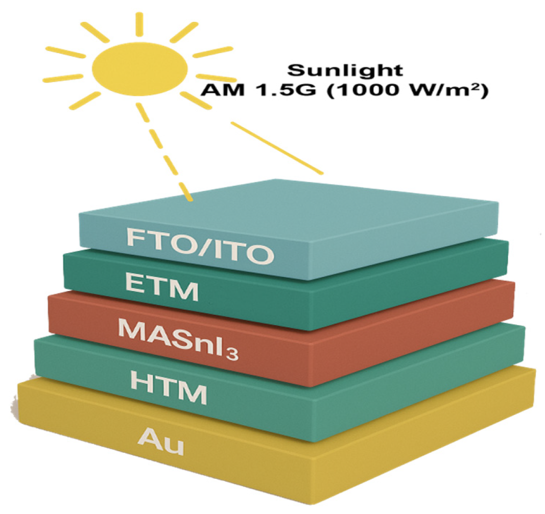
This study employed (Solar Cell Capacitance Simulator) SCAPS-1D (version 3.3.10), a specialized 1D software for simulating solar cell behavior. SCAPS-1D enables the numerical analysis of solar cells by incorporating up to seven distinct layers, allowing customization of physical properties such as bandgap, electron affinity, and dielectric permittivity [20,21]. This flexibility allows for in-depth exploration of different configurations and physical parameters. The software supports both Alternating Current (AC) and Direct Current (DC) simulations, including Current-Voltage (I-V) characteristics and complex impedance (Z*) analysis across a range of conditions, such as varying bias voltages, illumination, and temperatures. The proposed solar cell structure is FTO/ZnO/MASnI3/NiOx/Au, where each layer has a specific function. The FTO layer serves as the transparent contact, ZnO facilitates electron transport, and MASnI3 acts as the absorber generating charge carriers. The NiOx layer functions as the Hole Transport Layer (HTL) Figure 1.
Figure 1.
Schematic layout of PSCs of FTO/ZnO/MASnI3/NiOx/Au.
The simulation of the FTO/ZnO/MASnI3/NiOx/Au heterostructure solar cell involves the utilization of specific physical parameters, as outlined in Table 1. The physical parameters used were selected based on a careful survey of previously published experimental and simulation studies on MASnI3-based PSCs and their transport layers (ZnO, NiOx, FTO). In particular, the bandgap, electron affinity, dielectric permittivity, density of states, and carrier mobilities were adopted from well-established reports that combine experimental characterization with SCAPS-1D simulations [20,22,23,24].
Table 1.
Physical parameters of different layers.
Additionally, Table 2 provides details regarding the physical properties of defects density in MASnI3 [25]. Defect densities were chosen within experimentally realistic ranges (1015–1017 cm−3 for bulk layers and ~1010 cm−2 for interfaces), consistent with reported values for tin-based perovskites and metal-oxide transport layers. These values ensure numerical stability and physical consistency while allowing the simulation to reproduce experimentally observed current densities, voltages, and impedance trends. Alternative parameter sets were tested during preliminary simulations, but the values reported in Table 1 provided the best agreement with reported device performance and impedance behavior in the literature. Simulations were conducted under standard AM 1.5G spectrum solar illumination at 300 K, and specific physical parameters of each layer and interface properties were outlined to study their effects on cell efficiency and impedance.
Table 2.
Interface parameters.
It should be noted that the present study is based exclusively on SCAPS-1D numerical simulations and does not include new experimental device fabrication or measurements. The aim of this work is not to reproduce a specific experimental PSC, but rather to provide a physically consistent interpretation of bias-dependent impedance and relaxation phenomena in MASnI3-based devices. All material parameters and interface properties employed in the simulations were adopted from experimentally validated literature, and the simulated trends are consistent with previously reported experimental impedance spectroscopy results. While direct experimental comparison would further strengthen the analysis, the present simulation-supported approach offers valuable mechanistic insight and serves as a predictive framework to guide future experimental investigations.
3. Results and Discussion
3.1. Optimization of Bias Voltage
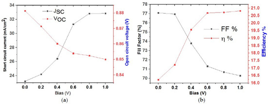
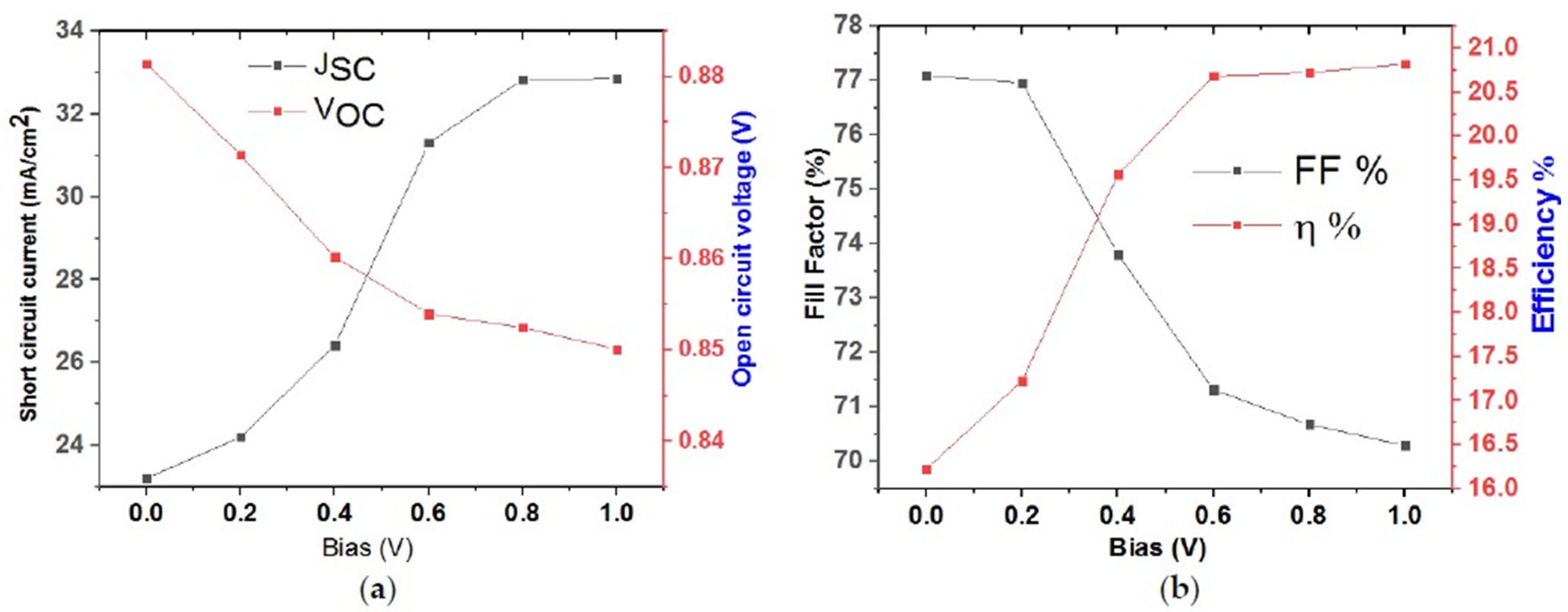
Applying a bias voltage influences how charges and dipoles respond within PSCs. It modifies the internal electric field, which slows carrier relaxation and enhances interfacial polarization effects. These changes appear as longer relaxation times in impedance spectra. Studying this bias dependence helps clarify the link between charge transport dynamics and interfacial stability. Figure 2 illustrates how bias voltage influences key photovoltaic parameters of the FTO/ZnO/MASnI3/NiOx/Au device. Figure 2a shows the variation in JSC versus bias. As the bias voltage increases, the short-circuit current initially stays high (around 32 mA/cm2) at low voltages and then decreases as the voltage approaches 1 V. This suggests that the current generation at the cells electrodes drops as the external voltage rises, likely due to increased recombination or reduced charge separation at higher voltages. In contrast, the Voc increases from approximately 0.84 V to 0.88 V as the bias voltage increases, reflecting the voltage at which the cell can no longer produce a current. The small increase in VOC with voltage indicates improved potential difference between the electrodes as the bias voltage rises.
Figure 2.
Bias-Dependent evolution in MASnI3-Based Solar Cells (a) Jsc, Voc, (b) FF %, and Efficiency.
Figure 2b shows the variation in Fill Factor (FF) versus bias, which measures how close the solar cells IV curve is to an ideal rectangular shape. It starts high (~77%) and decreases to around 70% as the bias voltage increases. This drop suggests a loss of ideality in the IV characteristics as the bias voltage increases, possibly due to parasitic resistances or non-ideal recombination processes. Figure 2b shows the variation in Efficiency (η) versus bias. It starts low (~16%), increases to a maximum of about 21% at a moderate bias, and then slightly drops again. This peak corresponds to an optimal operating voltage, after which efficiency decreases as the cell’s performance starts to degrade, likely due to increased recombination losses or sub-optimal extraction of charges.
3.2. Complex Impedance Analysis
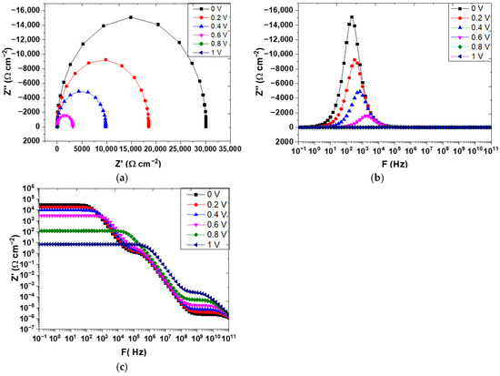
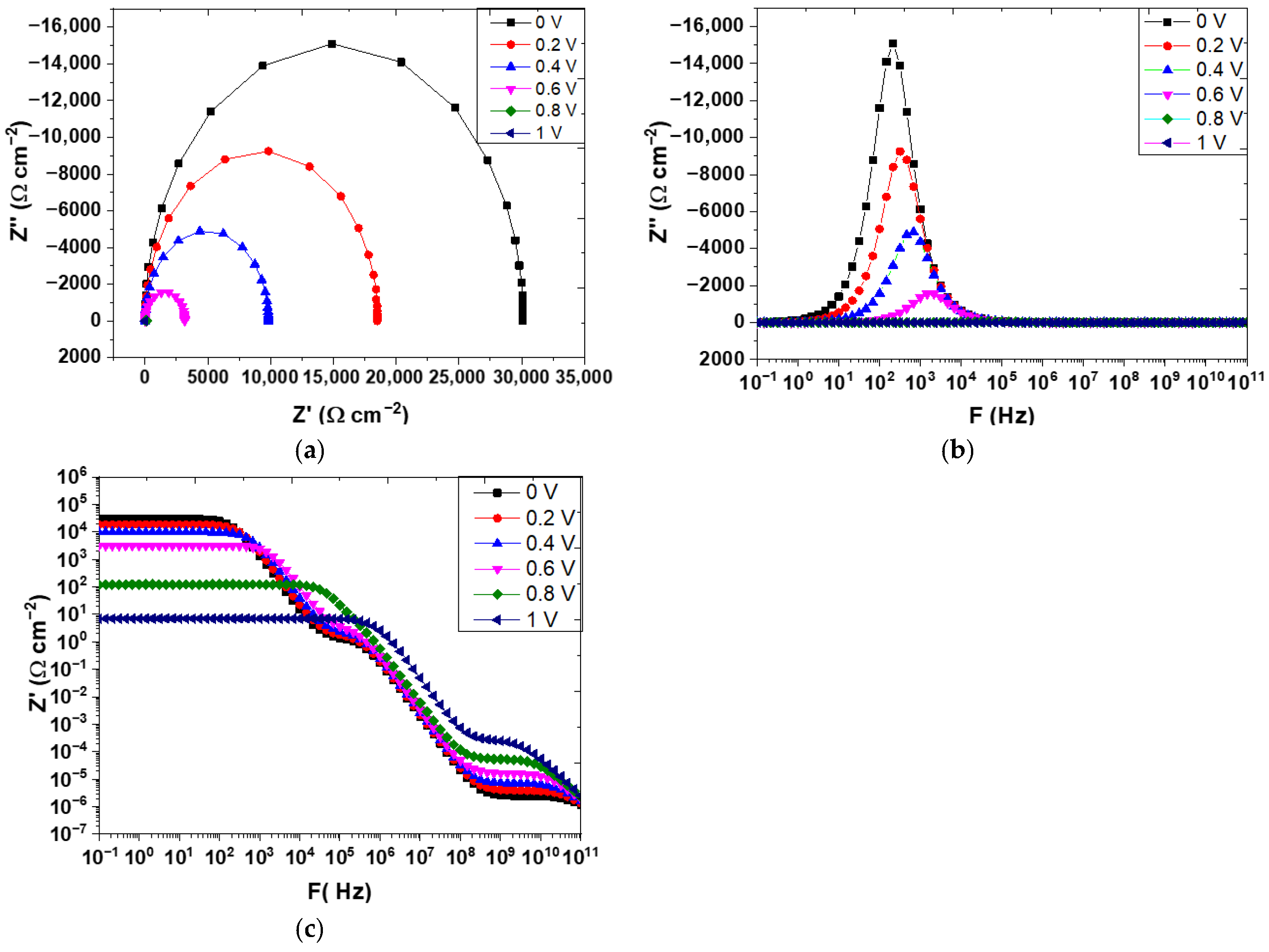
The impedance spectra presented in Figure 3 illustrate the evolution of the electrical response of the FTO/ZnO/MASnI3/NiOx/Au PSC under increasing bias voltage. In the Nyquist plot (Figure 3a), each curve exhibits a single, well-defined semicircular arc whose radius systematically decreases as the applied bias voltage increases from 0 V to 1 V. This progressive shrinkage reflects a significant reduction in charge-transfer resistance (Rct) at the active interfaces, indicating that the applied electric field enhances carrier mobility and facilitates more efficient charge extraction across the device. At zero bias, the large arc diameter suggests limited carrier transport, high recombination activity, and possible charge accumulation at defect-rich regions or interfacial trap sites. The corresponding high values of both the real (Z′) and imaginary (Z′′) impedance components imply sluggish interfacial kinetics and hindered charge separation, which is typical of unassisted or equilibrium conditions in perovskite layers.
Figure 3.
Impedance spectra of PSC at different bias: (a) Nyquist plot (b) and (c) bode plots.
As the forward bias increases, the arcs become smaller and shift toward the origin, revealing that the internal potential barrier between the transport layers and the perovskite absorber is lowered. This bias-assisted field accelerates carrier extraction, reduces recombination losses, and enhances the overall conductivity of the device. The improvement in interfacial transport behavior correlates closely with the observed rise in short-circuit current (Jsc) and efficiency at moderate bias levels. Beyond 0.8 V, however, the stabilization of the semicircle size may indicate a saturation regime, where further bias produces diminishing improvements due to the onset of ionic polarization or defect recharging processes.
The semicircular pattern arises from a characteristic RC (resistor–capacitor) time constant behavior, where the system acts capacitively at low frequencies (charge accumulation or polarization) and resistively at higher frequencies (ohmic conduction). This response is typically attributed to a dominant relaxation process involving bulk charge recombination and interfacial diffusion in the perovskite and transport layers. Similar trends have been reported by Mortadi et al. [12] and Wu et al. [26], who observed that in both lead-free and lead-halide perovskite architectures, the forward bias effectively reduces Rct while extending relaxation times due to bias-induced polarization effects. The decreasing arc radius with bias thus represents a dual effect: enhanced electronic transport and concurrently increased interfacial polarization, both critical for understanding how bias voltage modulates the dynamic behavior of FTO/ZnO/MASnI3/NiOx/Au solar cells.
In the Bode plots (Figure 3b,c), complementary insights into the device dynamics are revealed through the frequency-dependent variation of the impedance components. The phase-angle spectra (Figure 3b) display a distinct relaxation peak whose position shifts systematically with the applied bias voltage. At low bias (0–0.2 V), the peak appears at relatively high frequencies, corresponding to faster electronic processes and limited polarization effects. As the bias increases, the characteristic peak gradually moves toward higher frequencies, indicating shorter relaxation times for the dominant electronic processes. This trend suggests that higher bias voltages induce more pronounced interfacial polarization and ionic redistribution within the perovskite layer, likely caused by the migration of mobile ions such as Sn2+ vacancies or halide defects toward the transport interfaces. These slow-moving species accumulate under forward bias, altering local electric fields and producing delayed charge compensation, which manifests as longer relaxation times in the impedance response.
The magnitude spectra (Figure 3c) further support this interpretation. The real part of the impedance (Z′) shows a characteristic slope change over specific frequency ranges, revealing the coexistence of multiple relaxation processes. At mid-to-high frequencies, the impedance decreases sharply, indicating dominance of electronic charge transport through the perovskite bulk and transport layers. At lower frequencies, however, the impedance remains relatively high and exhibits a more gradual slope, reflecting slow interfacial or ionic polarization phenomena. The appearance of these features confirms that, in addition to the main relaxation associated with bulk recombination, a secondary low-frequency process becomes active under bias most likely linked to trap-assisted recombination or ion accumulation at the ZnO/MASnI3 and MASnI3/NiOx interfaces. This dual relaxation behavior implies that the system transitions from being electronically limited at low bias to polarization-limited at higher bias. The observed frequency shift of the Z′′ peaks indicates that while charge transport accelerates under moderate bias (reducing recombination losses), ionic and dipolar reorientation processes progressively dominate at stronger fields, leading to extended relaxation times. Such behavior is consistent with the bias-dependent impedance characteristics reported by [26], who demonstrated that the competition between carrier transport and ionic migration governs the low-frequency tail of the impedance spectra. Similarly, Zhang et al. [27] employed Bayesian Distribution of Relaxation Times (DRT) analysis to show that forward bias can separate overlapping time constants corresponding to electronic and ionic processes a phenomenon clearly reflected in the present results.
Overall, the Bode analysis confirms that bias voltage modifies both the kinetics and polarization mechanisms within the ZnO/MASnI3/NiOx solar cell. At moderate bias, carrier extraction is enhanced and recombination minimized; at higher bias, the accumulation of mobile ions and dipolar species extends the relaxation time, introducing strong interfacial polarization effects. This interplay between charge transport and bias-induced polarization plays a decisive role in the overall impedance response and directly impacts the dynamic stability and efficiency of lead-free perovskite devices.
3.3. Modulus Function and Relaxation Process Analysis
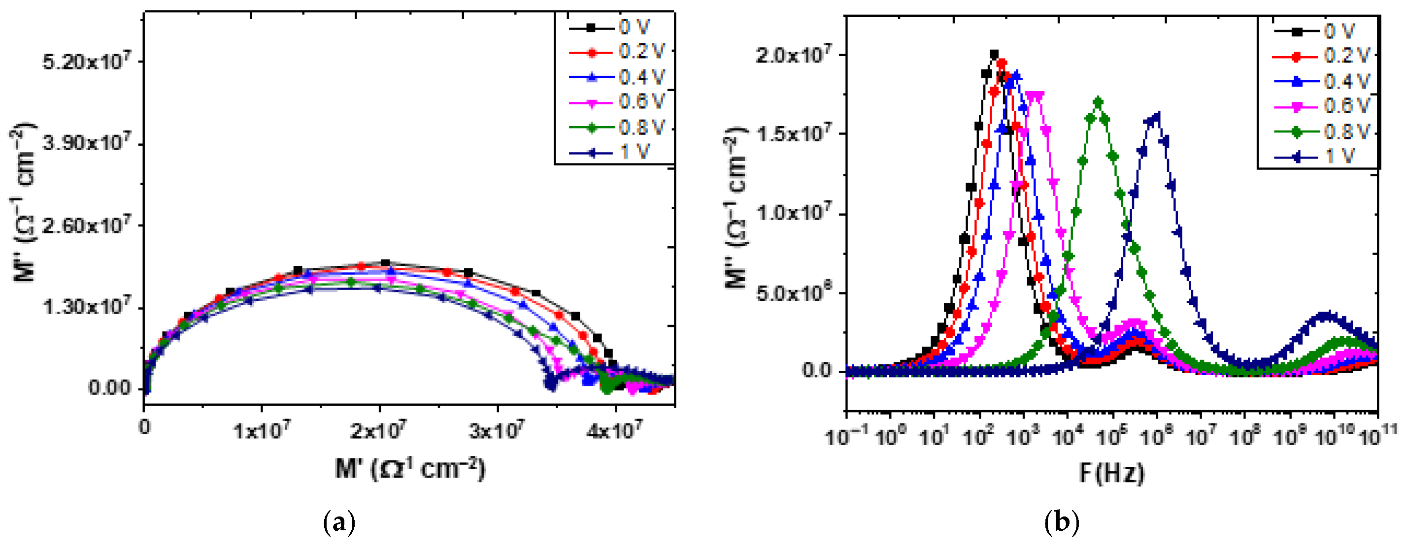
The modulus spectra (Figure 4) provide a complementary perspective on the charge-transport and relaxation dynamics within the PSC under different applied bias voltages (0–1 V). In the Nyquist representation of the complex modulus (M*) (Figure 4a), each curve exhibits a semicircular arc that flattens and shrinks progressively with increasing bias. These flattened arcs, characteristic of modulus analysis, indicate a distribution of relaxation times rather than a single relaxation process, highlighting the coexistence of multiple charge transport pathways in the device. The largest semicircle at 0 V suggests a strong capacitive response caused by charge accumulation or trapping at the interfaces, while the reduction in arc size at higher bias points to improved charge transport and diminished capacitive effects due to enhanced carrier extraction under stronger electric fields.
Figure 4.
Modulus spectra of the PSC at bias voltage (a) Nyquist plot and (b) bode plots.
The Bode plots of the imaginary part of the modulus (M″) (Figure 4b), further clarify the nature of the relaxation phenomena. Three distinct frequency peaks are observed for each bias voltage, indicating the presence of three major relaxation processes operating at different time scales. At 0 V, these peaks appear at lower frequencies, corresponding to longer relaxation times and slower dynamic responses within the system. As the applied bias increases, all peaks shift toward higher frequencies, implying shorter relaxation times and faster charge dynamics a clear sign that forward bias facilitates more efficient carrier transport and suppresses slow ionic or trap-mediated processes.
The first peak, located at low frequencies, is attributed to slow charge migration and accumulation within the bulk perovskite layer. This process is strongly influenced by ionic motion, such as halide or Sn2+ vacancy migration, and is more pronounced at low bias when the driving electric field is weak. The second peak, appearing at intermediate frequencies, is associated with interface polarization and trap-assisted relaxation, possibly occurring at grain boundaries or at the interfaces between the perovskite and transport layers. Such effects arise from localized charge trapping and detrapping processes that slow down the response of the system. The third, high-frequency peak corresponds to rapid electronic relaxation linked to charge injection and extraction at the electrode–perovskite interfaces, where dynamics are dominated by electronic processes with minimal ionic involvement.
These three relaxation processes collectively describe the hierarchical charge dynamics of the PSCs. At low bias, slow bulk and interfacial processes dominate, leading to higher resistive and capacitive components. With increasing bias, the semicircles in the modulus Nyquist plot become smaller and more compressed, indicating that electronic transport becomes more efficient while ionic and trap-related effects are partially mitigated. The observed peak shifts and arc compression thus reveal how the applied bias modulates both the resistive-capacitive behavior and the frequency-dependent relaxation mechanisms within the device.
Generally, the modulus function analysis highlights the multiscale nature of relaxation phenomena in the FTO/ZnO/MASnI3/NiOx/Au PSC. The results demonstrate that bias voltage not only enhances carrier mobility but also reorganizes the internal electric field, accelerating high-frequency electronic responses while simultaneously reducing low-frequency ionic polarization. These insights emphasize that optimizing PSC performance requires a comprehensive approach addressing all three regimes: (i) improving perovskite crystallinity and reducing defect densities to mitigate slow bulk relaxation, (ii) engineering stable interfaces to suppress polarization effects at intermediate frequencies, and (iii) refining electrode contacts to maximize charge transfer efficiency at high frequencies. Such understanding, consistent with recent reports by [28,29,30,31,32] provides valuable guidance for designing next-generation lead-free PSCs with enhanced dynamic stability and efficiency.
3.4. Modeling via Electrical Equivalent Circuit
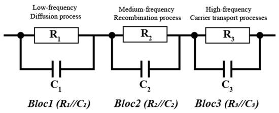
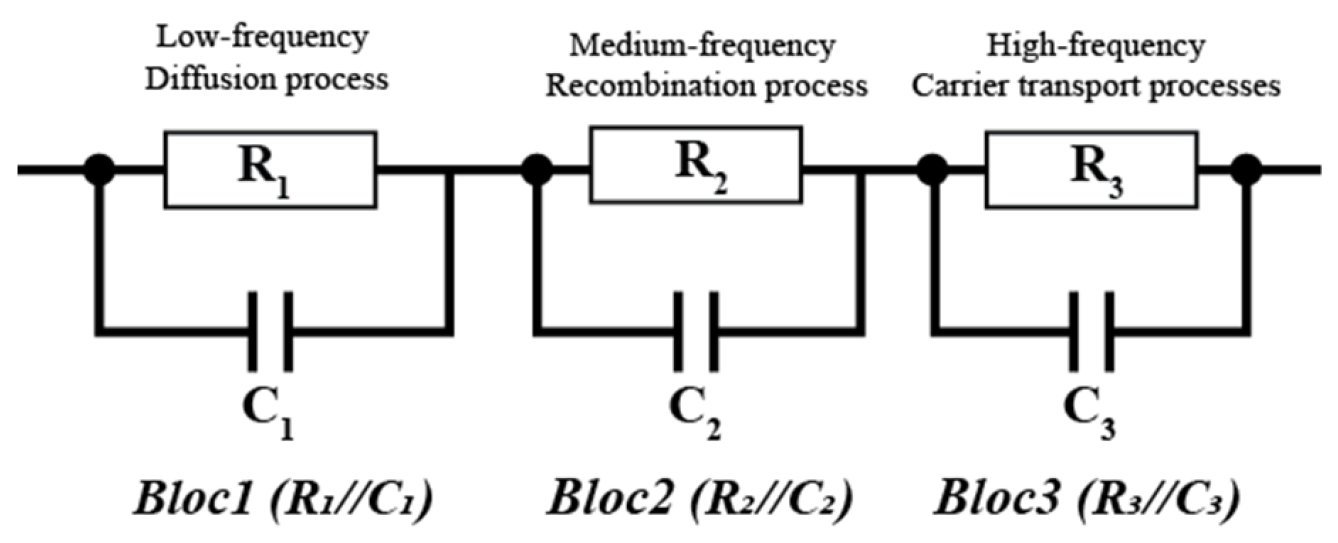
The equivalent electrical circuit shown in Figure 5 is designed to model the impedance behavior of a PSC by replicating key physical processes, including charge transport, recombination, and interface effects. It consists of three Resistor-Capacitor (RC) pairs connected in series, where each pair corresponds to a specific relaxation process observed in the experimental Nyquist and Bode plots. The choice of this circuit is based on a thorough analysis of both impedance and electric modulus spectra. As clearly shown in Figure 3c, a change in slope is observed, indicating the presence of three distinct processes. This interpretation is further confirmed by the modulus spectra analysis, where three well-defined relaxation processes are clearly observed in both the Nyquist and Bode plots.
Figure 5.
Equivalent electrical circuit of the PSC.
It is well established in the literature that each semicircle or relaxation process can be modeled by a parallel RC circuit. Therefore, the presence of three relaxation processes justifies the use of three RC loops connected in series in the proposed equivalent circuit.
Regarding the parameter values, we have chosen to present them in terms of the relaxation times for each loop, defined as τi = RiCi, in order to avoid redundancy in the presentation of the results.
The resistor R1 and capacitor C1 represent the slow processes, such as charge migration or recombination within the bulk perovskite material. R2 and C2 model intermediate-frequency phenomena, such as polarization effects at interfaces or grain boundaries. Finally, R3 and C3 capture the high-frequency dynamics related to charge transfer at the interfaces between electrodes and the active layer. This arrangement allows for fitting the experimental data by associating each RC pair with a distinct relaxation process. The resistors model the dissipative losses (resistance to charge flow), while the capacitors account for the storage of electrical energy and polarization effects. Together, they provide an accurate representation of the complex impedance (Z*) and modulus (M*) spectra, offering insights into the solar cell’s performance and limiting factors.
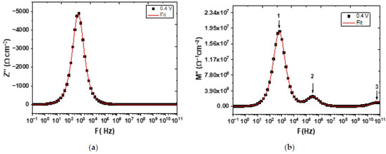
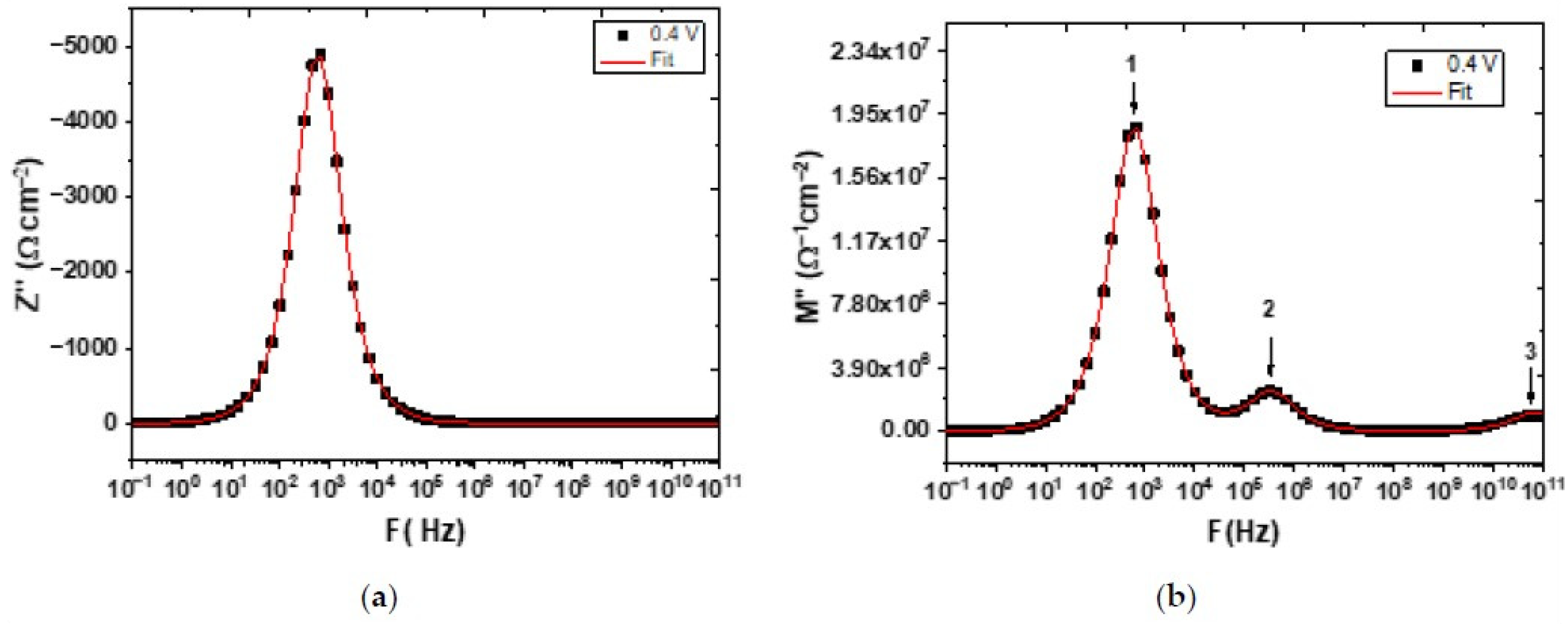
Figure 6 presents the comparison between the simulated impedance response and the fitting results obtained using the proposed equivalent electrical circuit (Figure 5) at an applied bias voltage of 0.4 V. The excellent agreement between the simulated data and the fitted curves for both the imaginary part of the impedance (Z″) and the imaginary part of the electric modulus (M″) confirms the physical relevance and robustness of the chosen circuit model.
Figure 6.
Fit of process in the PSC at 0.4 V versus frequency (F): (a) imaginary part of impedance Z″ and (b) imaginary part of modulus M″.
In Figure 6a, the Z″ spectrum exhibits a dominant relaxation peak located in the intermediate-frequency range. This peak reflects a resistive–capacitive (RC) process governed primarily by charge recombination and transport across the perovskite absorber and its adjacent interfaces. Within the framework of the equivalent circuit (Figure 5), this response is mainly described by the R2–C2 branch, which accounts for interfacial polarization and trap-assisted recombination processes occurring at the ZnO/MASnI3 and MASnI3/NiOx interfaces. The accurate reproduction of both the peak position and amplitude demonstrates that the intermediate-frequency dynamics are correctly captured by this RC element.
Figure 6b provides further insight through the modulus representation (M″), which is particularly sensitive to bulk-related relaxation phenomena and suppresses electrode-dominated contributions. Three distinct peaks are clearly resolved and labeled (1), (2), and (3), confirming the presence of three independent relaxation processes operating at different characteristic frequencies. These peaks directly correspond to the three RC pairs introduced in the equivalent circuit of Figure 5.
The low-frequency peak (1) is associated with the R1–C1 branch, representing slow processes such as ionic migration and space-charge accumulation within the MASnI3 bulk. These processes dominate the long-time response of the device and are typically linked to mobile ionic species and defect-related polarization effects.
The intermediate-frequency peak (2) corresponds to the R2–C2 branch, which models interfacial charge trapping, polarization, and recombination dynamics. This contribution plays a critical role under operational bias conditions, where accumulated charges at interfaces modify local electric fields and influence overall device performance.
The high-frequency peak (3) arises from the R3–C3 branch and is attributed to fast electronic processes, including charge injection and extraction at the electrode–transport layer interfaces. These dynamics are dominated by electronic carriers and exhibit minimal ionic involvement, leading to short relaxation times.
The simultaneous fitting of Z″ and M″ using the same circuit parameters demonstrates the internal consistency of the model and confirms that the separation of relaxation processes into low-, intermediate-, and high-frequency regimes is physically justified rather than arbitrary. Importantly, while Z″ emphasizes recombination and resistive losses, M″ highlights bulk and dielectric relaxation effects, making their combined analysis essential for a comprehensive interpretation.
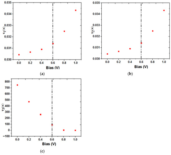
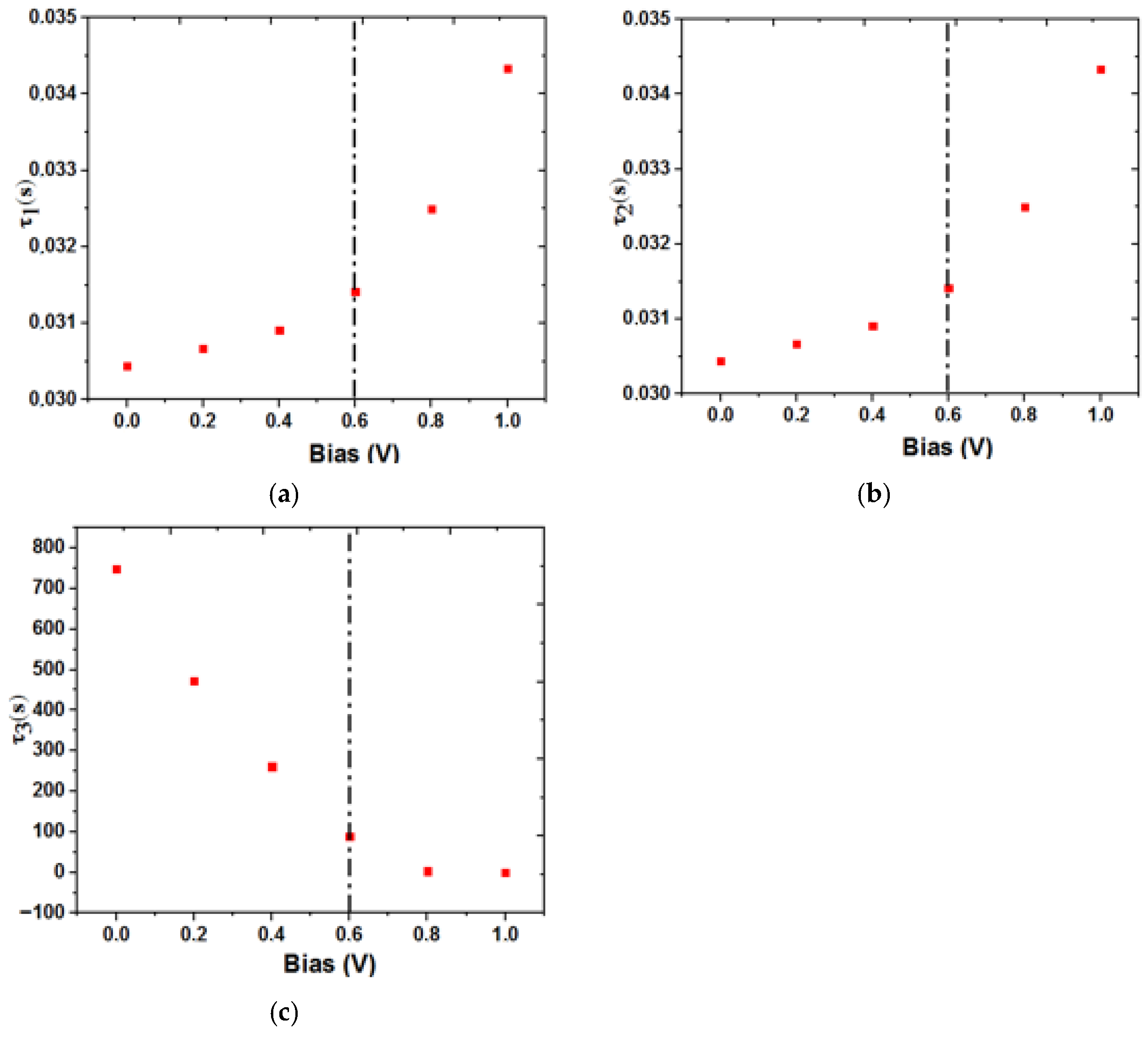
In Figure 7, we observe the variation in relaxation times for different physical effects in a MASnI3 PSC as a function of applied bias voltage, ranging from 0 V to 1 V. These relaxation times are associated with three primary processes: charge transport, recombination, and interface effects. In Figure 7a, the relaxation time associated with charge transport (τ1) increases gradually as the bias voltage rises. At low biases (around 0 V to 0.4 V), charge carriers (electrons and holes) move relatively efficiently, resulting in shorter relaxation times. However, as the bias approaches 0.8 V, τ1 stabilizes at a higher value, suggesting that the mobility of charge carriers decreases with increasing bias. This could be due to enhanced scattering or bottlenecks in charge extraction, as the built-in electric field becomes less effective at pulling charges through the perovskite layer. Thus, at higher biases, the charge transport slows down, possibly contributing to a reduction in solar cell performance under strong illumination or at higher operational voltages. In Figure 7b, we see the relaxation time related to recombination (τ2), which follows a trend similar to that of charge transport. At lower biases, recombination is fast, as the proximity of charge carriers encourages them to recombine. However, as the bias voltage increases, the separation of carriers is enhanced, reducing their recombination probability. This result in a slight increase in τ2, indicating that the recombination process becomes less dominant as the cell operates at higher biases. This trend aligns with the expected behavior of solar cells, where efficient charge separation and extraction reduce the likelihood of recombination losses, especially at voltages close to the Voc. Figure 7c presents the relaxation time for interface effects (τ3), which exhibits the most pronounced change with bias. At low bias (up to around 0.4 V), τ3 is relatively low, suggesting that charge transfer across the interfaces (such as the perovskite/transport layer interface) is efficient. However, as the bias increases beyond 0.6 V, τ3 rises dramatically. This sharp increase points to a growing influence of interface-related bottlenecks, possibly due to the accumulation of space charges or higher resistance at the interfaces. At these higher voltages, the interfaces become a limiting factor in overall cell performance, as they impede the extraction of charges, slowing down the overall dynamics of the cell.
Figure 7.
Relaxation time at bias voltage: (a) charge transport, (b) recombination, and (c) interface effects.
In summary, the relaxation times for charge transport, recombination, and interface effects all increase with bias voltage, indicating that the dynamics of the MASnI3 PSC become more constrained at higher operational voltages. While the slower recombination process is beneficial for improving cell efficiency, the increasing relaxation times for charge transport and interface effects highlight potential challenges in achieving optimal performance. These results emphasize the importance of optimizing both the bulk properties and the interfaces of PSCs to enhance their efficiency and stability, particularly under high operational voltages.
4. Conclusions
In this work, a bias-dependent impedance and modulus spectroscopy analysis of FTO/ZnO/MASnI3/NiOx/Au PSCs was carried out using SCAPS-1D simulations to elucidate charge-transport and relaxation mechanisms that are not directly accessible from standard current–voltage analysis. By jointly analyzing the complex impedance (Z*) and electric modulus (M*) responses, three distinct relaxation regimes were unambiguously identified and associated with bulk charge transport, interfacial polarization/recombination, and electrode charge injection processes.
The results demonstrate that increasing forward bias does not simply enhance carrier extraction but also induces a redistribution of relaxation times, with a progressive dominance of interfacial and polarization-related processes at higher voltages. In particular, the strong bias dependence of the low- and intermediate-frequency relaxation times highlights the critical role of ionic migration and interface charging in limiting device performance under operational conditions. The proposed equivalent circuit, incorporating three RC elements, provides a physically consistent representation of these multi-scale processes and enables quantitative interpretation of the impedance spectra.
Although this study is based on numerical simulations, all observed trends are consistent with experimentally reported impedance behaviors in both lead-based and lead-free PSCs. The present work therefore offers a predictive and interpretative framework that complements experimental impedance spectroscopy and helps clarify how bias-induced polarization and interfacial effects govern the dynamic response of MASnI3-based devices. These insights underline the necessity of interface engineering and defect control to suppress slow polarization processes and improve the operational stability and efficiency of lead-free PSCs. Future work will focus on direct experimental validation of the proposed relaxation model.
Author Contributions
Y.T.: investigation, data curation, formal analysis, writing—original draft preparation, writing—review and editing; H.L. and H.N.: software, formal analysis; A.M.: supervision, visualization, data curation, writing—review and editing. All authors will be updated at each stage of manuscript processing, including submission, revision, and revision reminder, via emails from our system or the assigned Assistant Editor. All authors have read and agreed to the published version of the manuscript.
Funding
This research received no external funding.
Institutional Review Board Statement
Not applicable.
Informed Consent Statement
Not applicable.
Data Availability Statement
The original contributions presented in the study are included in the article. Further inquiries can be directed to the corresponding author.
Conflicts of Interest
The authors declare that they have no known competing financial interests or personal relationships that could have appeared to influence the work reported in this paper.
References
- Pandey, L.; Kumar, D.; Parkash, O.; Pandey, S. Analytical Impedance Spectroscopy: Basics and Applications; CRC Press: Boca Raton, FL, USA, 2023. [Google Scholar]
- Karmakar, S. Impedance spectroscopy for electroceramics and electrochemical system. arXiv 2024, arXiv:2406.15467. [Google Scholar]
- Zhang, B.; Wang, L.; Zhang, Y.; Wang, X.; Qiao, Y.; Sun, S.-G. Reliable impedance analysis of Li-ion battery half-cell by standardization on electrochemical impedance spectroscopy (EIS). J. Chem. Phys. 2023, 158, 054202. [Google Scholar] [CrossRef] [Scilit]
- Magar, H.S.; Hassan, R.Y.; Mulchandani, A. Electrochemical impedance spectroscopy (EIS): Principles, construction, and biosensing applications. Sensors 2021, 21, 6578. [Google Scholar] [CrossRef] [Scilit]
- Jarwal, D.K.; Kumar, A.; Mishra, A.K.; Ratan, S.; Upadhyay, R.K.; Kumar, C.; Mukherjee, B.; Jit, S. Fabrication and TCAD validation of ambient air-processed ZnO NRs/CH3NH3PbI3/spiro-OMeTAD solar cells. Superlattices Microstruct. 2020, 143, 106540. [Google Scholar] [CrossRef] [Scilit]
- Bhatt, V.; Kumar, M.; Yadav, P.; Kumar, M.; Yun, J.-H. Low cost and solution processible sandwiched CH3NH3PbI3-xClx based photodetector. Mater. Res. Bull. 2018, 99, 79–85. [Google Scholar] [CrossRef] [Scilit]
- Mortadi, A.; El Hafidi, E.; Monkade, M.; El Moznine, R. Investigating the influence of absorber layer thickness on the performance of perovskite solar cells: A combined simulation and impedance spectroscopy study. Mater. Sci. Energy Technol. 2024, 7, 158–165. [Google Scholar] [CrossRef] [Scilit]
- EHauff, V.; Klotz, D. Impedance spectroscopy for perovskite solar cells: Characterisation, analysis, and diagnosis. J. Mater. Chem. C 2022, 10, 742–761. [Google Scholar]
- Arif, H.; Tahir, M.B.; Sagir, M.; Alrobei, H.; Alzaid, M.; Ullah, S.; Hussien, M. Effect of potassium on the structural, electronic, and optical properties of CsSrF3 fluro perovskite: First-principles computation with GGA-PBE. Optik 2022, 259, 168741. [Google Scholar] [CrossRef] [Scilit]
- Mishra, K.K.; Chahar, S.; Sharma, R. An extensive investigation of structural, electronic, and optical properties of inorganic perovskite Ca3AsCl3 for photovoltaic and optoelectronic applications: A first-principles approach using Quantum ATK tool. Solid State Commun. 2024, 390, 115623. [Google Scholar] [CrossRef] [Scilit]
- Shafiq, M.; Tahir, M.B.; Ahmed, B.; Dahshan, A.; Ali, H.E.; Sagir, M. DFT screening of Ga-dopped ScInO3 perovskite for optoelectronic and solar cell applications. Inorg. Chem. Commun. 2024, 161, 112054. [Google Scholar] [CrossRef] [Scilit]
- Mortadi, A.; El Hafidi, E.; Nasrellah, H.; Monkade, M.; El Moznine, R. Analysis and optimization of lead-free perovskite solar cells: Investigating performance and electrical characteristics. Mater. Renew. Sustain. Energy 2024, 13, 219–232. [Google Scholar] [CrossRef] [Scilit]
- Mortadi, A.; Nasrellah, H.; Monkade, M.; El Moznine, R. Investigation of bandgap grading on performances of perovskite solar cell using SCAPS-1D and impedance spectroscopy. Sol. Energy Adv. 2024, 4, 100056. [Google Scholar] [CrossRef] [Scilit]
- Chen, C.; Fu, Q.; Guo, P.; Chen, H.; Wang, M.; Luo, W.; Zheng, Z. Ionic transport characteristics of large-size CsPbBr3 single crystals. Mater. Res. Express 2019, 6, 115808. [Google Scholar] [CrossRef] [Scilit]
- Hua, Y.; Sun, X.; Li, X.; Cui, F.; Yue, Z.; Liu, J.; Liu, H.; Zhang, G.; Tao, X. Anisotropic X-ray detection performance of melt-grown CsPbBr 3 single crystals. J. Mater. Chem. C 2023, 11, 9153–9160. [Google Scholar] [CrossRef] [Scilit]
- Mortadi, A.; Tabbai, Y.; El Hafidi, E.; Nasrellah, H.; Chahid, E.; Monkade, M.; El Moznine, R. Investigating temperature effects on perovskite solar cell performance via SCAPS-1D and impedance spectroscopy. Clean. Eng. Technol. 2025, 24, 100876. [Google Scholar] [CrossRef] [Scilit]
- Zhang, L.; Dai, Y.; Li, C.; Dang, Y.; Zheng, R.; Wang, Z.; Wang, Y.; Cui, Y.; Arandiyan, H.; Shao, Z. Recent advances in electrochemical impedance spectroscopy for solid-state batteries. Energy Storage Mater. 2024, 69, 103378. [Google Scholar] [CrossRef] [Scilit]
- Wang, Z.; Wang, Y.; Py, B.; Maradesa, A.; Liu, J.; Wan, T.H.; Saccoccio, M.; Ciucci, F. DRTtools: Freely Accessible Distribution of Relaxation Times Analysis for Electrochemical Impedance Spectroscopy. ACS Electrochem. 2025, 1, 2680–2689. [Google Scholar] [CrossRef] [Scilit]
- Mortadi, A.; Tabbai, Y.; Lizoul, B.; Salhi, I.; Chahid, E.H.; Nasrellah, H.; Mghaiouin, R.; Chahid, E.G. Comprehensive Investigation of Relative Permittivity Effects on Perovskite Solar Cell Performance Using SCAPS-1D and Impedance Spectroscopy. Eng 2025, 6, 371. [Google Scholar] [CrossRef] [Scilit]
- Adewoyin, A.D.; Olopade, M.A.; Oyebola, O.O.; Chendo, M.A. Development of CZTGS/CZTS tandem thin film solar cell using SCAPS-1D. Optik 2019, 176, 132–142. [Google Scholar] [CrossRef] [Scilit]
- Aliaghayee, M. Optimization of the Perovskite Solar Cell Design with Layer Thickness Engineering for Improving the Photovoltaic Response Using SCAPS-1D. J. Electron. Mater. 2023, 52, 2475–2491. [Google Scholar] [CrossRef] [Scilit]
- Saha, P.; Singh, S.; Bhattacharya, S. Performance optimization of MASnI3 perovskite solar cells: Insights into device architecture. Micro Nanostruct. 2024, 191, 207827. [Google Scholar] [CrossRef] [Scilit]
- Sahani, R.; Pandey, S.K. A Comparative Study of Different MASnI3-Based Perovskite Solar Cells to Identify an Optimized and Stable PSC Structure. J. Electron. Mater. 2025, 54, 8732–8744. [Google Scholar] [CrossRef] [Scilit]
- Jayan, K.D.; Sebastian, V. Comprehensive device modelling and performance analysis of MASnI3 based perovskite solar cells with diverse ETM, HTM and back metal contacts. Sol. Energy 2021, 217, 40–48. [Google Scholar] [CrossRef] [Scilit]
- You, J.; Meng, L.; Song, T.-B.; Guo, T.-F.; Yang, Y.; Chang, W.-H.; Hong, Z.; Chen, H.; Zhou, H.; Chen, Q. Improved air stability of perovskite solar cells via solution-processed metal oxide transport layers. Nat. Nanotechnol. 2016, 11, 75–81. [Google Scholar] [CrossRef] [Scilit]
- Wu, J.; Yang, C.; Luo, Z.; Wang, X.; Zheng, F.; Zhao, Z.; Hu, Z. Unified model for describing the evolution of negative capacitance in perovskite solar cells. Phys. Rev. Appl. 2024, 22, 024041. [Google Scholar] [CrossRef] [Scilit]
- Zhang, Y.; Chen, Y.; Yan, M.; Chen, F. Reconstruction of relaxation time distribution from linear electrochemical impedance spectroscopy. J. Power Sources 2015, 283, 464–477. [Google Scholar] [CrossRef] [Scilit]
- Chen, R.; Wang, J.; Liu, Z.; Ren, F.; Liu, S.; Zhou, J.; Wang, H.; Meng, X.; Zhang, Z.; Guan, X. Reduction of bulk and surface defects in inverted methylammonium-and bromide-free formamidinium perovskite solar cells. Nat. Energy 2023, 8, 839–849. [Google Scholar] [CrossRef] [Scilit]
- Al-Shujaa, S.; Zhao, P.; He, D.; Al-Anesi, B.; Feng, Y.; Xia, J.; Zhang, B.; Zhang, Y. Improving the efficiency and stability of perovskite solar cells by refining the perovskite-electron transport layer interface and shielding the absorber from UV effects. ACS Appl. Mater. Interfaces 2024, 16, 28493–28504. [Google Scholar] [CrossRef] [Scilit] [PubMed]
- Tao, J.; Ali, N.; Chen, K.; Huai, Z.; Sun, Y.; Fu, G.; Kong, W.; Yang, S. Enhanced efficiency in perovskite solar cells by eliminating the electron contact barrier between the metal electrode and electron transport layer. J. Mater. Chem. A 2019, 7, 1349–1355. [Google Scholar] [CrossRef] [Scilit]
- Wang, Z.; Gu, L.; Zou, M.; Zhang, H.; Zhou, Q. Surface Engineering in Perovskite Solar Cells: Recent Advances in Surface Passivation Group-Containing Hole Transport Layers. Langmuir 2025, 41, 13705–13725. [Google Scholar] [CrossRef] [Scilit]
- Ma, T.; Wang, H.; Wu, Z.; Zhao, Y.; Chen, C.; Yin, X.; Hu, L.; Yao, F.; Lin, Q.; Wang, S. Hole transport layer-free low-bandgap perovskite solar cells for efficient all-perovskite tandems. Adv. Mater. 2024, 36, 2308240. [Google Scholar] [CrossRef] [Scilit] [PubMed]

Disclaimer/Publisher’s Note: The statements, opinions and data contained in all publications are solely those of the individual author(s) and contributor(s) and not of MDPI and/or the editor(s). MDPI and/or the editor(s) disclaim responsibility for any injury to people or property resulting from any ideas, methods, instructions or products referred to in the content. |
© 2026 by the authors. Licensee MDPI, Basel, Switzerland. This article is an open access article distributed under the terms and conditions of the Creative Commons Attribution (CC BY) license.