


Abstract
To meet the requirements of wide-temperature reliability and fast transient response in power management ICs for automotive, aerospace, and industrial applications, this paper presents a fast-response low-dropout regulator (LDO) based on a 0.18 μm high-temperature SOI process. Benefiting from the buried oxide isolation structure of the SOI technology, leakage current and parasitic effects under high-temperature conditions are effectively suppressed. The proposed LDO employs an NMOS power transistor, with an on-chip charge pump used to enhance the gate driving capability. In addition, a triple-loop regulation scheme consisting of a main negative feedback loop, an auxiliary positive feedback loop, and a current-mode feedback loop is adopted to improve transient performance and enhance loop stability. The fabricated chip occupies an area of 2840 μm × 1490 μm and supports an input voltage range of 3–5.5 V and an output voltage range of 1.2–3.3 V. Over a temperature range of −55 °C to 175 °C, the LDO can deliver a maximum load current of 400 mA. At 175 °C, the measured overshoot and undershoot voltages are 64 mV and 94 mV, respectively, with a maximum recovery time of 336 μs. Moreover, the power supply rejection ratio (PSRR) reaches 56.8 dB at 100 Hz. Experimental results demonstrate that the proposed LDO exhibits excellent high-temperature adaptability, strong load-driving capability, and superior transient response performance.
1. Introduction
With the continuous development of electronic systems toward high reliability, high power density, and operation in extreme environments, the ability of power management circuits to maintain stable performance under high-temperature conditions has become increasingly critical. As a key module in power management integrated circuits, the low-dropout regulator (LDO) is widely used in automotive electronics, aerospace systems, industrial control, and geothermal exploration due to its low output noise, simple structure, and good transient performance. In these application scenarios, electronic systems are often required to operate continuously in high-temperature or even ultra-high-temperature environments, which imposes more stringent requirements on the high-temperature reliability and dynamic regulation performance of LDOs.
Conventional LDOs are typically implemented using bulk CMOS processes. However, bulk silicon devices are prone to increased leakage current, threshold voltage drift, enhanced parasitic effects, and a higher risk of latch-up under high-temperature conditions. These issues can lead to degraded output accuracy, slower transient response, increased power consumption, and even circuit failure. In contrast, Silicon-On-Insulator (SOI) technology provides electrical isolation between the device and the substrate through a buried oxide layer, which effectively reduces parasitic leakage currents, suppresses latch-up effects, and improves the stability of device parameters under high-temperature conditions. Therefore, SOI technology has become an important foundation for high-temperature integrated circuits and high-temperature LDO design.
Existing studies have verified the high-temperature applicability of SOI technology. Petrosyants et al. evaluated the electrical characteristics of small-scale SOI MOSFETs at temperatures up to 300 °C, demonstrating that they can still maintain good current drive capability and threshold voltage stability [1,2]. Grella et al. further showed that 1 μm SOI CMOS devices can operate properly at temperatures as high as 450 °C [3]. Kappert et al. also confirmed the reliable operation of 0.35 μm SOI CMOS technology over a wide temperature range from 0 °C to 450 °C [4]. These studies indicate that SOI devices offer significant advantages in reducing leakage current, suppressing parasitic effects, and improving high-temperature stability, thereby providing a solid device foundation for high-temperature analog circuits and power management circuits [5,6,7].
At present, several low-dropout regulators designed for high-temperature environments have been reported. Texas Instruments’ TPS76901 (Texas Instruments Incorporated, 12500 TI Boulevard, Dallas, TX, USA) is implemented using a bulk CMOS process with a PMOS power transistor and operates over a temperature range of −55 °C to 210 °C. Its estimated lifetime at 210 °C is approximately six months, indicating that although bulk CMOS technology can meet certain high-temperature requirements, long-term reliability remains limited. In comparison, CISSOID’s CHT-VEGA, Honeywell’s HTPLREG, and X-REL’s XTR70010 are all implemented using SOI technology. These products support maximum operating temperatures of 225 °C to 230 °C and can achieve an operational lifetime of approximately five years under high-temperature conditions, demonstrating the superior reliability of SOI technology in high-temperature power management applications.
On the other hand, research on fast-response LDOs has mainly focused on enhancing power transistor gate drive capability, suppressing parasitic capacitance effects, implementing dynamic biasing techniques, and optimizing feedback/feedforward architectures. Ho et al. proposed an active feedback and slew-rate enhancement structure that improves transient response by increasing the charging and discharging speed of the power transistor gate [8]. Nasrollahpour et al. introduced an overcurrent pull-up technique to reduce the equivalent time constant at the output node pole [9]. Ahmadi et al. employed a dual-OTA complementary structure to enhance switching speed through dynamic bias current modulation [10]. Baik et al. utilized a local positive feedback loop and a feedforward path to strengthen loop regulation during transient events [11]. In addition, Li et al. introduced a digitally assisted control scheme that dynamically enables the power transistor according to load current variations, thereby improving load regulation performance [12]. These studies demonstrate that significant progress has been made in circuit topology and transient enhancement techniques for fast-response LDOs; however, there remains room for further improvement in output overshoot, undershoot, and recovery time under large load current transients.
However, current research still struggles to simultaneously achieve high-temperature reliability, fast transient response, and loop stability. To address these challenges, this work proposes a fast-response LDO based on a 0.18 μm high-temperature SOI process. The proposed LDO employs an NMOS power transistor, an on-chip charge pump, and a triple-loop regulation scheme to enhance transient performance and maintain stability under high-temperature conditions. The remainder of the paper is organized as follows: Section 2 introduces the SOI process; Section 3 presents the circuit design and loop analysis; Section 4 discusses the layout and test results; Section 5 concludes the paper.
2. Silicon-On-Insulator (SOI) Process
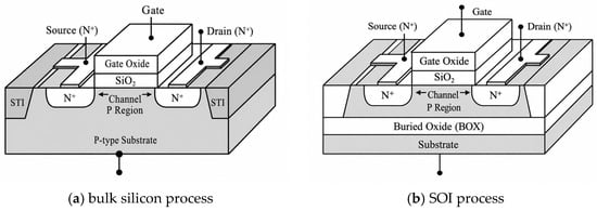
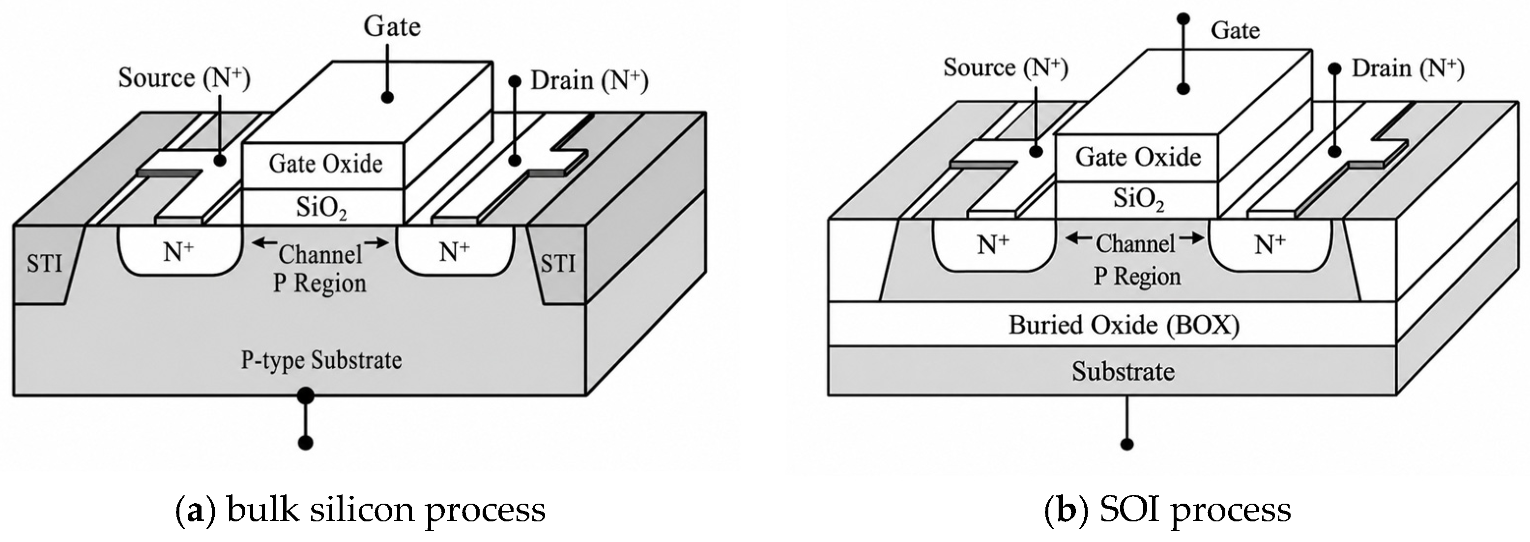
Conventional bulk CMOS N-well devices are directly fabricated on a silicon substrate, as shown in Figure 1a. In bulk silicon processes, there is a relatively large PN junction area between the source/drain regions and the substrate. Under high-temperature conditions, this structure tends to generate significant junction leakage current, accompanied by reduced carrier mobility, threshold voltage drift, and increased static power consumption, which limits its application in high-temperature integrated circuits.
Figure 1.
MOSFET structure.
In contrast, SOI CMOS devices form the MOS structure in a thin top silicon layer, where the active region is electrically isolated from the substrate by a buried oxide (BOX) layer, as shown in Figure 1b. This structure effectively reduces the junction area between the source/drain regions and the substrate, blocks part of the substrate leakage paths, and simultaneously reduces parasitic capacitance and suppresses the latch-up effect.
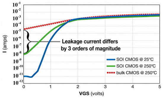
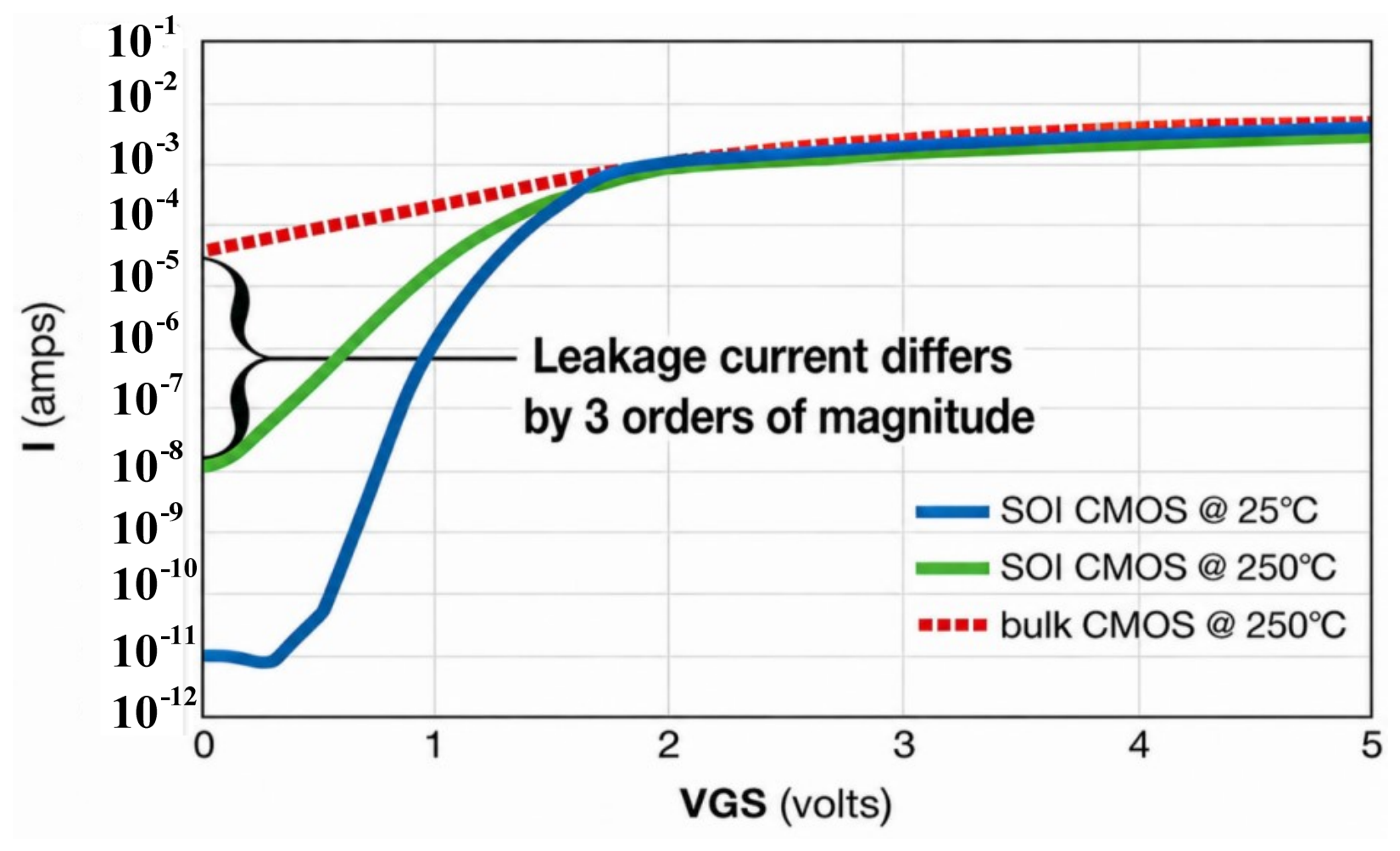
Thanks to the buried oxide (BOX) layer providing dielectric isolation and the reduced junction area, SOI devices can significantly suppress off-state leakage current under high-temperature conditions. As shown in Figure 2, compared with conventional bulk-silicon CMOS devices, the off-state leakage current of SOI devices can be reduced by approximately 2–3 orders of magnitude, which helps improve static power consumption characteristics, stability, and reliability in high-temperature environments. These advantages make SOI CMOS technology particularly suitable for high-temperature integrated circuit design and provide a critical process foundation for circuit operation at temperatures of 225 °C and above. Therefore, SOI technology has become an important process platform for high-temperature integrated circuit design and implementation.
Figure 2.
High-temperature leakage behavior of SOI and bulk-silicon devices.
3. Circuit Design
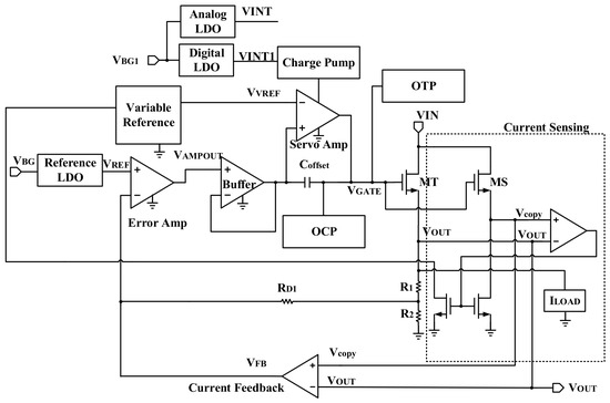
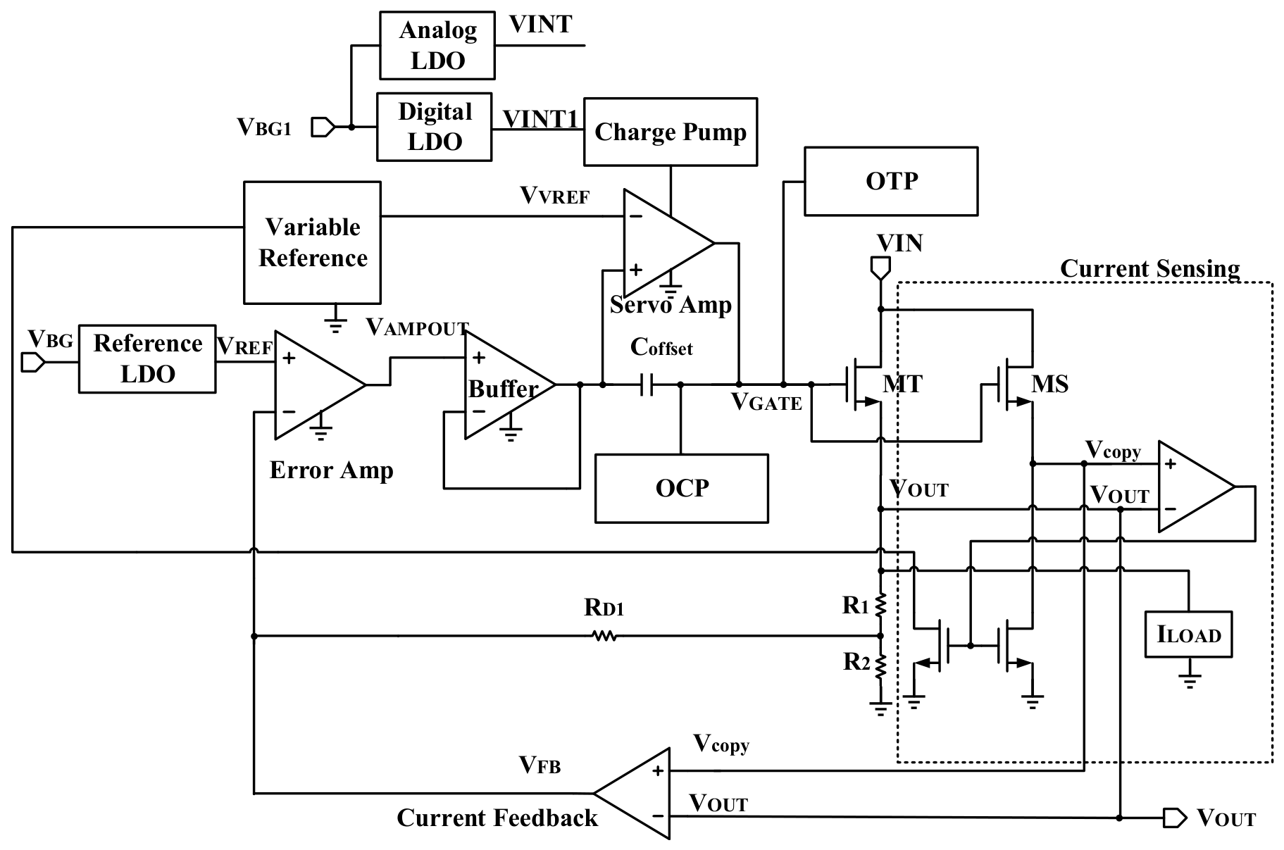
The basic topology of the proposed LDO circuit is shown in Figure 3. It consists of an NMOS power transistor, an on-chip integrated charge pump, three feedback loops, three internal LDO regulators, and two protection blocks. The main negative feedback loop includes an error amplifier, a buffer, and an offset capacitor Coffset. The auxiliary positive feedback loop is composed of a servo operational amplifier, a variable reference circuit, and a current sensing circuit. The current feedback network forms a current-mode negative feedback loop through external feedback resistors R1 and R2. To ensure reliable chip operation, over-temperature protection (OTP) and over-current protection (OCP) circuits are also implemented. In terms of power supply, the variable reference circuit, buffer, and error amplifier are powered by an internal low-voltage supply (VINT), which enhances the power supply rejection ratio (PSRR) of the loop. The servo operational amplifier is powered by a low-drive-capability on-chip charge pump.
Figure 3.
Structure of the LDO circuit.
In the auxiliary positive feedback regulation loop, the current sensing circuit detects the output current with a predefined scaling ratio and feeds the sensed current into the variable reference circuit to adaptively adjust the variable reference voltage VVREF. When the load current increases, the sensed current rises accordingly, leading to an increase in VVREF; conversely, when the load current decreases, VVREF decreases simultaneously. This voltage is applied to the negative input of the servo operational amplifier, while the output of the servo amplifier is connected to the gate of the NMOS power transistor, thereby forming an auxiliary positive feedback regulation path. To ensure system stability, a small sensing ratio is adopted in the design to limit the gain of this loop, keeping it lower than that of the main negative feedback loop.
When the load switches abruptly from light load to heavy load, VOUT momentarily drops, while both the variable reference voltage VVREF and the output voltage of the error amplifier VAMPOUT increase. Since the main negative feedback loop dominates the regulation behavior, the condition VAMPOUT > VVREF is typically satisfied. In this case, the servo operational amplifier charges the offset capacitor Coffset, raising the gate voltage of the NMOS power transistor and enhancing its conduction capability, thereby accelerating the recovery of the output voltage.
Conversely, when the load changes abruptly from heavy load to light load, both VVREF and VAMPOUT decrease, establishing the condition VAMPOUT < VVREF. The servo amplifier then discharges Coffset, reducing the gate voltage of the power transistor, which suppresses output overshoot and facilitates a fast recovery of VOUT.
After the servo operational amplifier adjusts the charge and discharge state of the offset capacitor, the main negative feedback loop rapidly responds by further regulating the output voltages of the error amplifier and buffer until VAMPOUT = VVREF is satisfied. Therefore, in steady state, the voltages at the positive and negative inputs of the servo operational amplifier converge to the same value, and the servo amplifier ceases to charge or discharge the offset capacitor.
It can be seen that the servo operational amplifier mainly acts on regulating the plate voltage across the offset capacitor Coffset and isolating the high-frequency noise introduced by the charge pump. The offset capacitor can be equivalently regarded as a floating voltage source, providing sufficient gate drive voltage for the power transistor, thereby ensuring that the NMOS power transistor operates in the saturation region under steady-state conditions.
In addition, the introduced current-mode negative feedback loop further improves the transient response capability of the chip under load variations.
3.1. Charge Pump
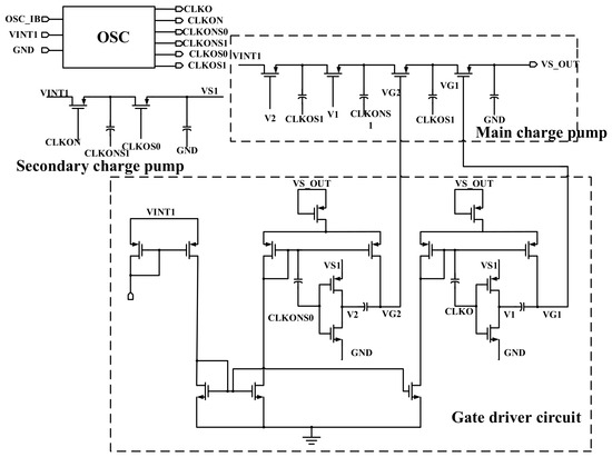
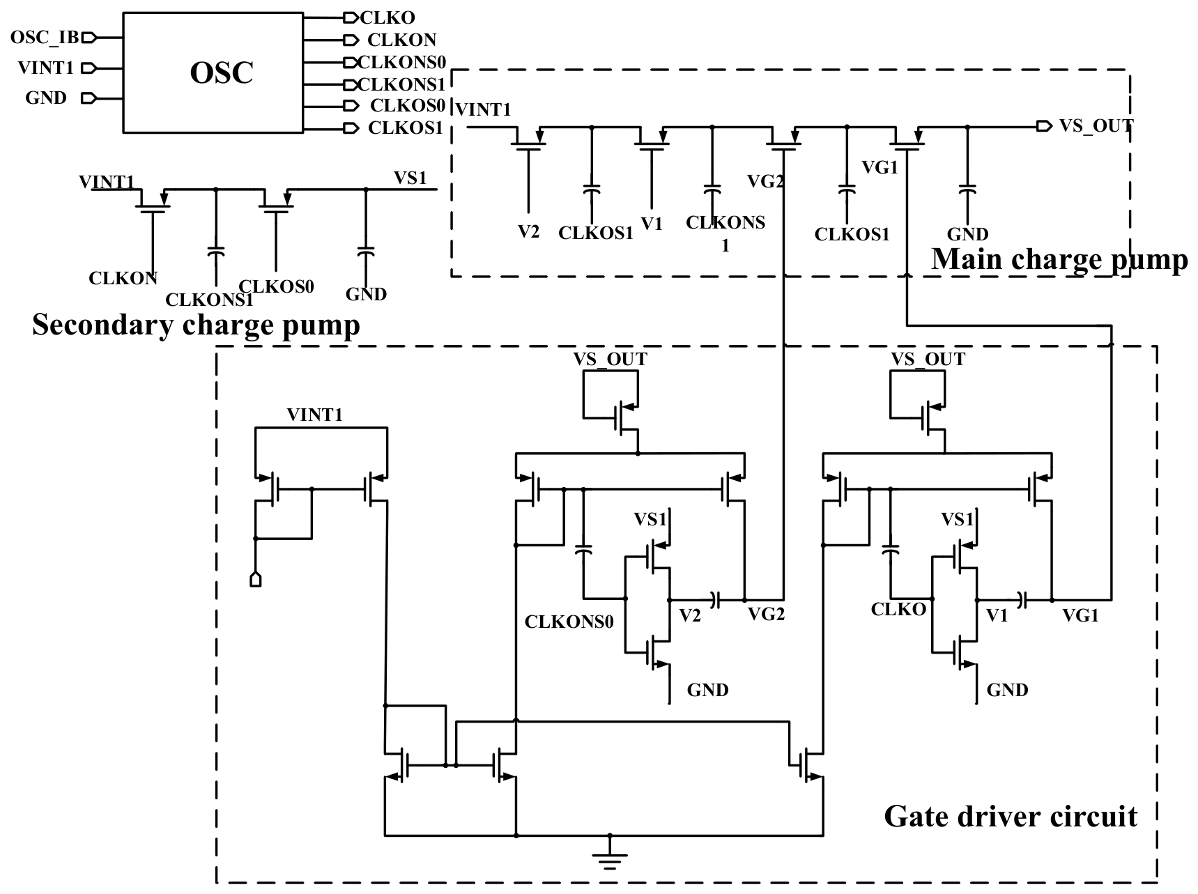
As shown in Figure 4, the designed charge pump module mainly consists of an oscillator, a secondary charge pump, a gate driver circuit, and a main charge pump. The oscillator (OSC) generates multi-phase non-overlapping clock signals, providing timing control for the periodic turn-on and turn-off of the switching transistors in each stage. The secondary charge pump adopts a first-stage Dickson switched-capacitor structure [13,14,15]. Using the internal supply VINT1 as its input, it generates a boosted node voltage VS1 through periodic charging and discharging of the pumping capacitor and charge transfer mechanisms. This provides a higher-than-VINT1 driving level for the gate driver circuit. The gate driver circuit generates gate control voltages VG1 and VG2 based on VS1 and the main charge pump output voltage VS_OUT, enabling precise control of the operating states of the PMOS switches in the main charge pump. This ensures reliable conduction during the charge transfer phase and effective turn-off during the bootstrapping phase, thereby reducing threshold voltage loss and suppressing reverse charge leakage. The main charge pump adopts a three-stage Dickson structure. Through cascaded PMOS switching devices and pumping capacitors, it achieves stepwise charge transfer and gradual elevation of node voltages under non-overlapping clock operation, ultimately producing a boosted output of approximately VS_OUT ≈ 3VINT1.
Figure 4.
Schematic diagram of the charge pump circuit.
3.2. Offset Capacitor
The offset capacitor is implemented using a CMOS capacitor. When the load undergoes a step change, assuming the variation at the buffer output is , due to the energy storage effect of the offset capacitor, the resulting voltage variation transferred to the power transistor gate is
where Coffset represents the capacitance value of the offset capacitor, and CG denotes the parasitic gate capacitance of the power transistor.
To enable fast transient response of the entire chip, the variation in the main negative feedback loop must be transferred accurately and rapidly. Therefore, the capacitance value of the offset capacitor Coffset should be much larger than the parasitic gate capacitance CG of the power transistor.
3.3. Servo Operational Amplifier
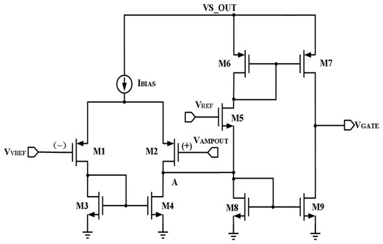
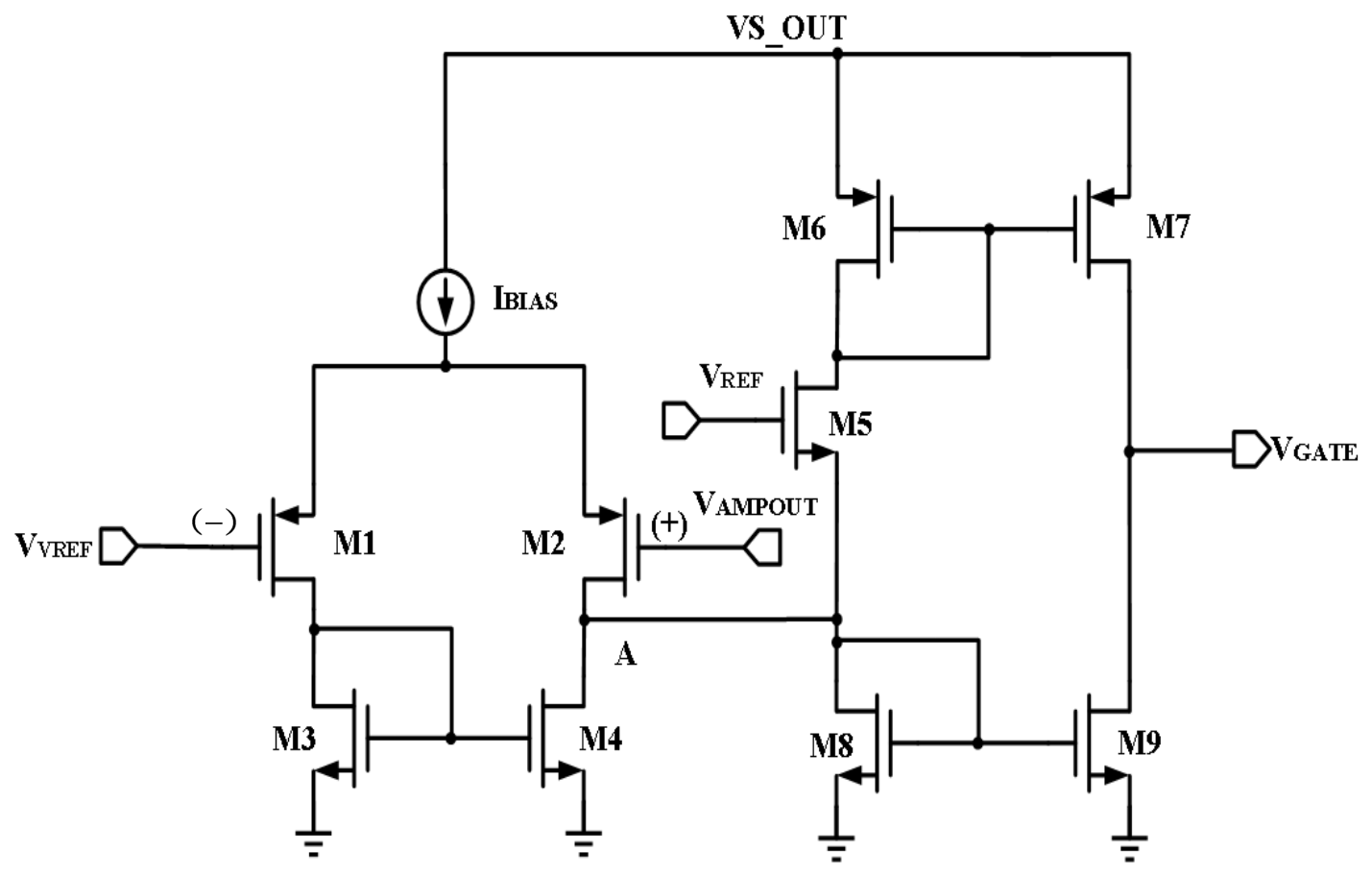
The schematic of the servo operational amplifier is shown in Figure 5. The left section consists of a conventional differential amplifier input stage, while the right section forms a push–pull output stage.
Figure 5.
Schematic diagram of the servo operational amplifier.
When VAMPOUT = VVREF, the differential input pair operates in a balanced state, and the bias current IBIAS is approximately equally distributed between the M1 and M2 branches. Under this condition, there is no significant net current exchange between the charge pump and the VGATE node, and the voltage across the offset capacitor remains stable.
When VAMPOUT > VVREF, M1 turns on while M2 turns off. Consequently, M3 and M4 are turned on, pulling node A low, which causes M8 and M9 to turn off while M5 turns on. In this case, IBIAS is mainly mirrored through the M1 branch to M4, and is further transferred to M7 through M5 and the current mirror. As a result, the charge pump provides charging current to the VGATE node, thereby charging the offset capacitor.
When VAMPOUT < VVREF, M2 turns on while M1 turns off. M3 and M4 are turned off, causing node A to rise and turning on M8 and M9. In this condition, IBIAS mainly flows through the M2 branch into M8 and is mirrored to M9 through the current mirror, forming a discharge path at the VGATE node to discharge the offset capacitor.
3.4. Current Sensing
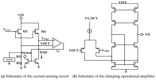
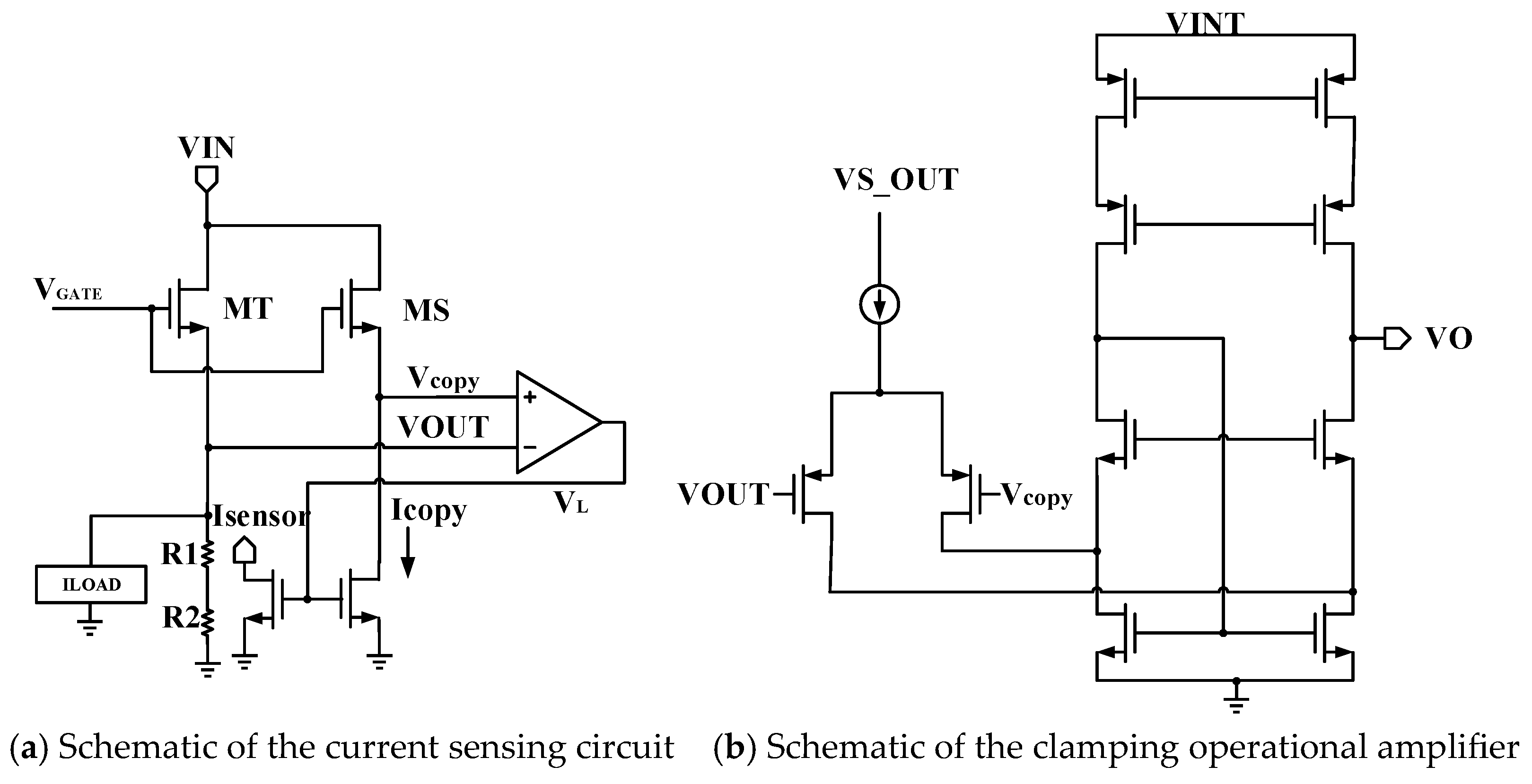
The current sensing circuit is shown in Figure 6a. The current of the power transistor MT is sensed by the sensing transistor MS with a scaling ratio K1. Here, K1 is defined as
Figure 6.
Schematic of the current sensing circuit.
The gate of the sensing transistor is connected to that of the power transistor, while the clamping operational amplifier ensures that the voltages of VOUT and Vcopy remain equal. The detailed circuit structure of the clamping operational amplifier is shown in Figure 6b. As a result, when the source voltage of the power transistor changes, the source voltage of the sensing transistor changes accordingly by the same amount.
The sensed current information, Isensor, is finally fed into the variable reference circuit, satisfying
3.5. Variable Reference
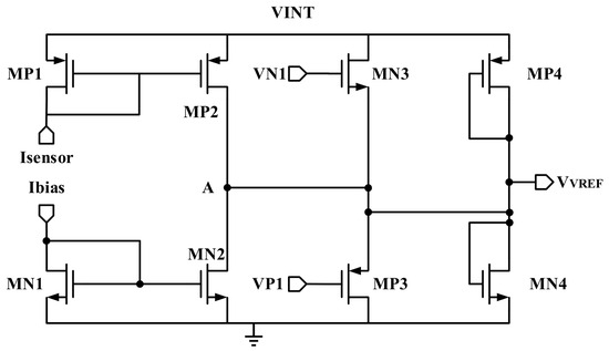
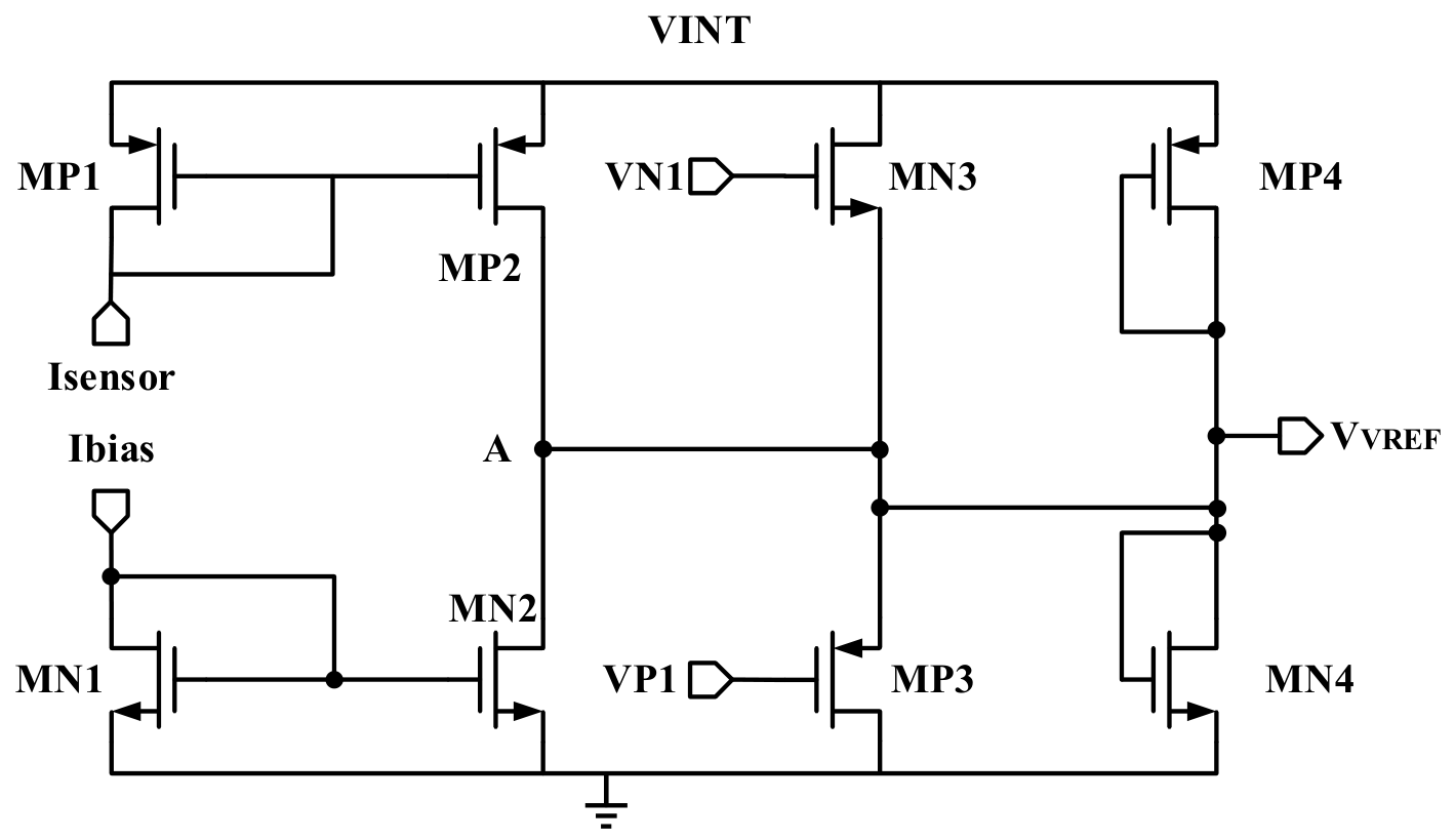
The variable reference circuit can adaptively adjust the output voltage VVREF according to changes in the load current, exhibiting a positive correlation characteristic in which the reference voltage increases as the load current increases. The schematic of the circuit is shown in Figure 7.
Figure 7.
Schematic diagram of the variable reference circuit.
Isensor is the dynamic current generated by the current sensing circuit, and Ibias is the bias current. VN1 and VP1 are the bias voltages in the error amplifier module.
When Isensor = Ibias, node A reaches a balanced state, and the output voltage is ideally approximately . However, due to the mismatch in impedance between MP2 and MN2, the output voltage may deviate from . Therefore, diode-connected transistors MP4 and MN4 are introduced to clamp the output voltage of the variable reference circuit to .
When Isensor > Ibias, node A is at a high potential, MP3 turns on, and the output voltage of the variable reference circuit is given by
When Isensor < Ibias, node A is at a low potential, MN3 turns on, and the output voltage of the variable reference circuit is given by
Thus, the output voltage range of the variable reference circuit can be expressed as
3.6. Current Feedback
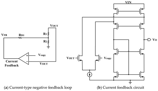
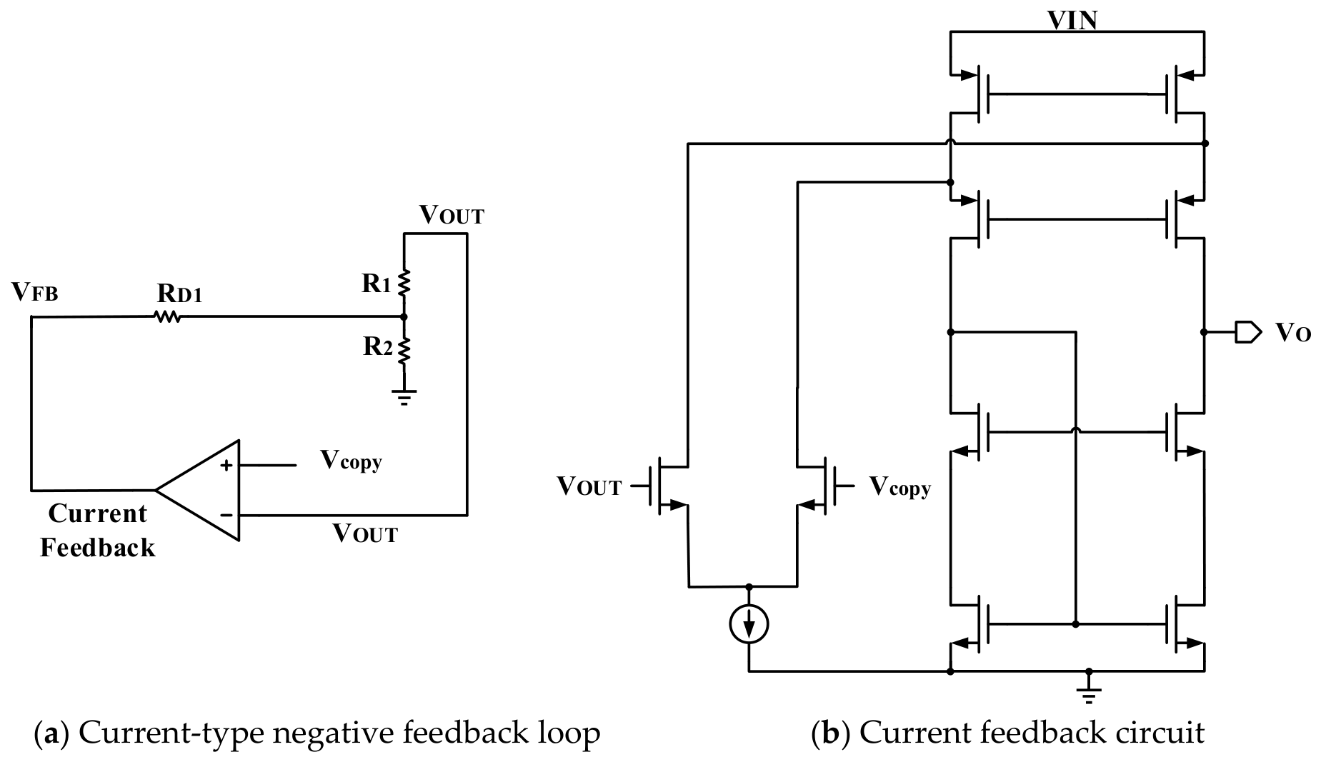
The current feedback circuit is mainly composed of an operational amplifier, and its schematic structure is shown in Figure 8a. This configuration, together with the resistive feedback network, forms another negative feedback path, and its feedback relationship is illustrated in Figure 8b.
Figure 8.
Current feedback circuit diagram.
When the load current switches from heavy load to light load, the output voltage VOUT rises instantaneously, and the feedback voltage VFB increases accordingly, while the sensing voltage Vcopy remains approximately unchanged due to response delay. In this case, the current feedback loop draws current from the R2 branch through the output of the operational amplifier, thereby reducing VFB, accelerating the recovery of the feedback node, and shortening the settling time of VOUT.
When the load current switches from light load to heavy load, the current feedback circuit injects a small-signal current into the R2 branch, driving VFB to increase. This enables the main feedback loop to enhance the drive capability of the power transistor more quickly, thereby facilitating the timely recovery of VOUT.
Therefore, with the introduction of the current-type negative feedback loop, the system can provide fast auxiliary regulation of the feedback node during load transients, thereby reducing output overshoot and undershoot and improving the load transient response performance of the LDO.
3.7. Loop Stability Analysis
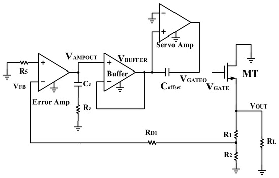
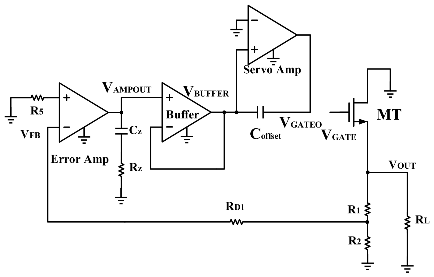
The equivalent loop of the LDO is shown in Figure 9. To improve the phase margin of the system, a compensation network and a unity-gain buffer are introduced into the loop. The unity-gain buffer features high input impedance and low output impedance, which shifts the pole at the output of the error amplifier to a higher frequency, preventing it from overlapping with the pole of the servo operational amplifier. The compensation network consists of a series resistor and capacitor connected between the output of the error amplifier and ground. It is used to introduce a compensating zero, thereby mitigating the reduction in phase margin caused by the close proximity of the output pole and the error amplifier pole under large load capacitance conditions.
Figure 9.
LDO equivalent loop.
The output pole of the LDO is given by
where gmPT is the transconductance of the power transistor, and COUT is the output capacitance of the LDO. Since the LDO is designed without an off-chip capacitor and the parasitic capacitance at the output node is very small, the output pole of the LDO is a high-frequency pole.
- (1)
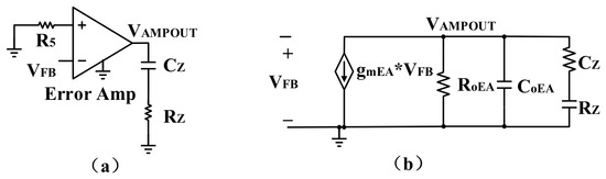
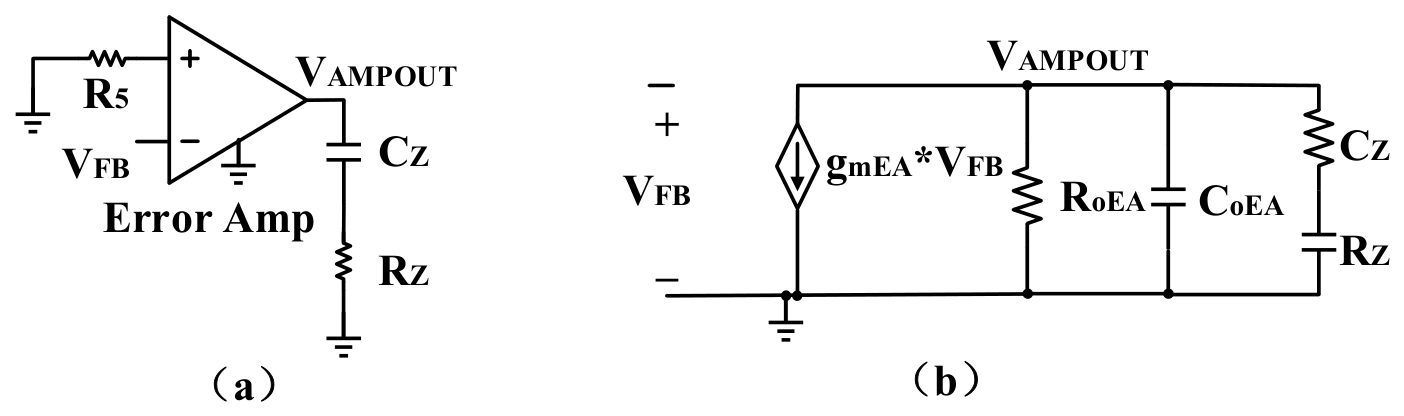
- The error amplifier and its small-signal model are shown in Figure 10. Transfer function derivation of the error amplifier and compensation networkFigure 10. Small-signal model of the error amplifier with compensation capacitor and resistor. (a) error amplifier; (b) Small-signal model of the error amplifier.
Therefore, the transfer function is given in Equation (8).
where gmEA is the transconductance of the error amplifier, CoEA is the output capacitance of the error amplifier, CZ is the compensation capacitor, and RZ is the compensation resistor. Therefore, the pole and zero introduced by the error amplifier and the compensation network are given by Equations (9), (10), and (11), respectively.
Since and , fp,AMP2 is located at a high frequency. By properly designing the value of RZ, this pole can be placed beyond the unity-gain bandwidth.
- (2)
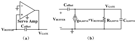
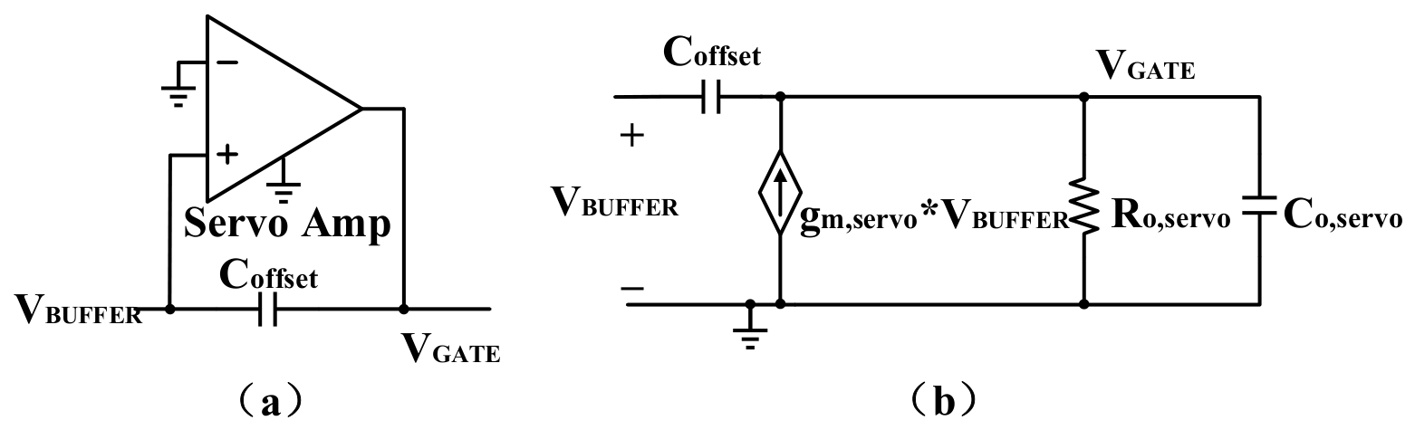
- The servo operational amplifier and its small-signal model are shown in Figure 11. Transfer function derivation of the servo operational amplifier and offset capacitorFigure 11. Small-signal model of the servo operational amplifier and offset capacitor. (a) servo operational amplifier; (b) small-signal model.
Therefore, the transfer function is given in Equation (12).
where gm,servo is the transconductance of the servo operational amplifier, Ro,servo is the output resistance of the servo operational amplifier, and Co,servo is the output capacitance of the servo operational amplifier.
From the transfer function, the pole and zero associated with the servo operational amplifier and the offset capacitor can be derived, as given in Equations (13) and (14), respectively.
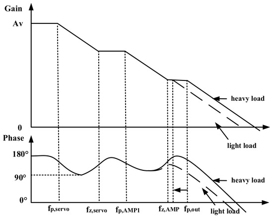
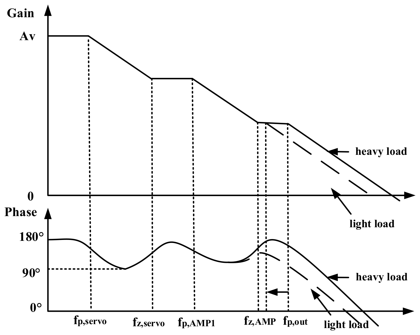
Since the quiescent current of the servo operational amplifier is relatively small, its transconductance gm,servo is small, while its output resistance Ro,servo is large. Therefore, the pole and zero of the servo operational amplifier are located at lower frequencies than those of the error amplifier, and the pole of the servo operational amplifier becomes the dominant pole in the low-frequency region.
The pole-zero distribution of the LDO loop is shown in Figure 12:
Figure 12.
Pole-zero distribution of the LDO loop.
4. Layout and Test Results
4.1. Layout Design
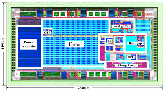
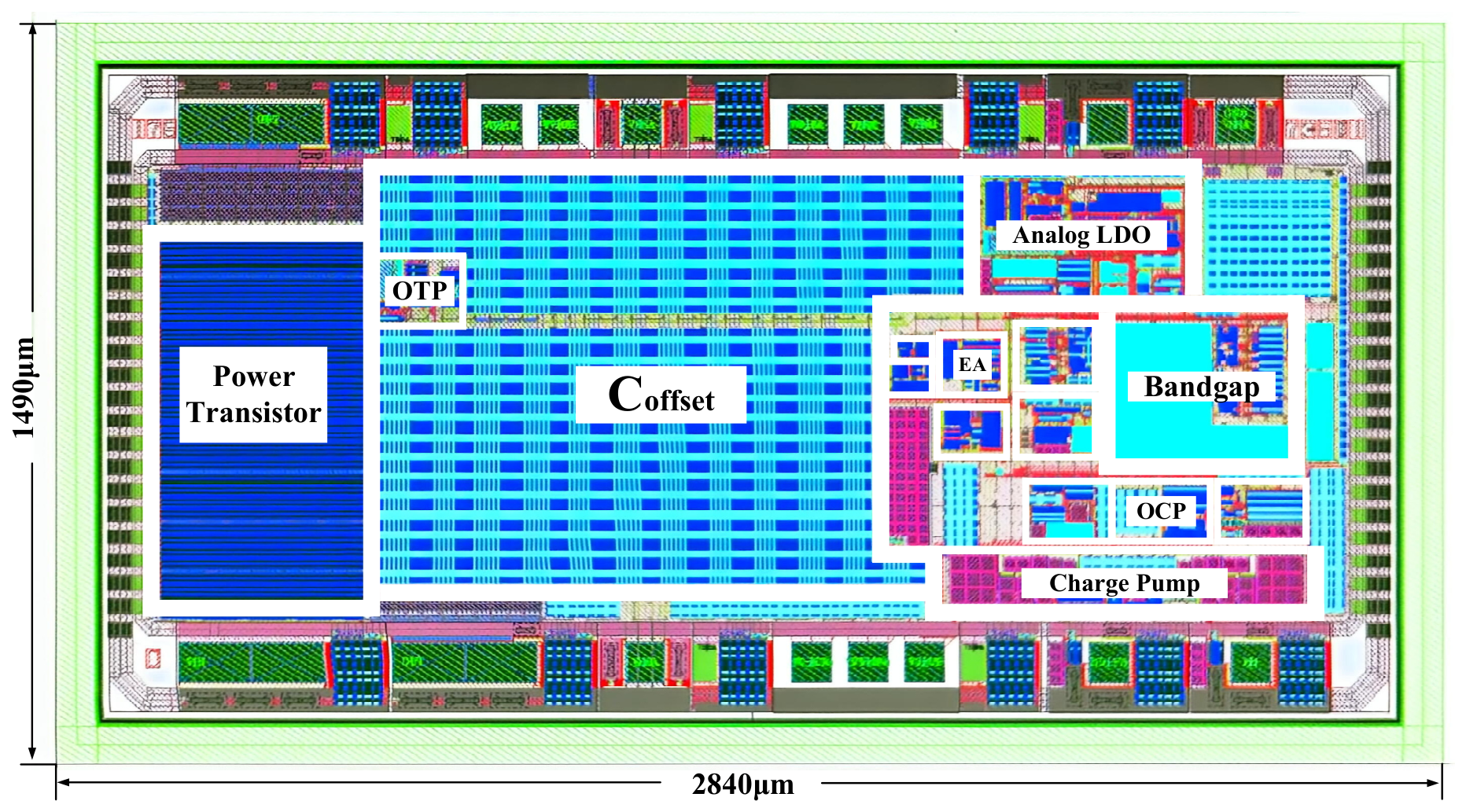
The LDO chip presented in this work is implemented using a 0.18 μm high-temperature SOI process. The overall chip area is 2840 μm × 1490 μm, and the layout is shown in Figure 13. The LDO operates with an input voltage range of 3–5.5 V and an adjustable output voltage range of 1.2–3.3 V. It can deliver a maximum load current of 400 mA, with a load capacitance of 0.1 μF, and operates over a temperature range of −55 to 175 °C.
Figure 13.
Overall layout.
The chip adopts a five-metal-layer layout. Metal 1 and Metal 2 are used for signal routing, Metal 3 for high-current paths, Metal 4 for power distribution, and the top metal layer as a ground plane to provide low-impedance return paths and improve ESD robustness. To support a maximum load current of 400 mA, the NMOS power transistor is implemented using a multi-finger structure. Wide metal routing, parallel via arrays, and a symmetrical current-sharing layout are employed to reduce parasitic resistance, improve current distribution, and enhance electromigration reliability under high-current operation.
4.2. Test Results
After fabrication, the chip was packaged in a SOT223-DCQ ceramic package and experimentally characterized. Electrical characterization was performed using an STS8205PLUS mixed-signal test system. Temperature-dependent measurements were conducted using a temperature chamber to provide controlled high- and low-temperature environments. In addition, a transient test platform consisting of a signal generator, programmable DC power supplies, precision measurement instruments, and an oscilloscope was employed to evaluate the transient response characteristics of the proposed LDO. All measurements were performed with a 0.1 μF output capacitor unless otherwise noted.
The temperature characterization was conducted over the range of −55 °C to 175 °C, which corresponds to the validated temperature range of the adopted SOI PDK device models. In addition, considering the reliability of the SOT223-DCQ ceramic package and the high-temperature test setup, 175 °C was selected as the upper characterization limit.
- A.
- Dropout voltage
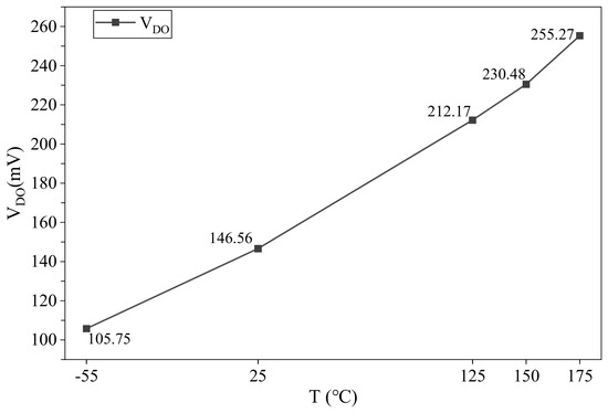
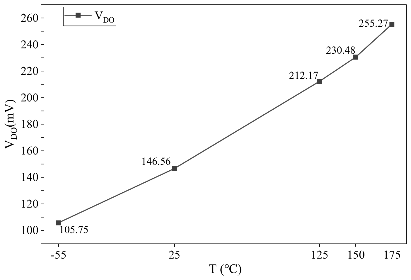
Figure 14 shows the measured dropout voltage under the conditions of VIN = 3.8 V, EN = 1.7 V, VOUT = 3.3 V, and ILOAD = 400 mA. The measured dropout voltages VDO at −55 °C, 25 °C, and 175 °C are 105.75 mV, 146.56 mV, and 255.27 mV, respectively.
Figure 14.
Temperature characteristics of dropout voltage test results.
- B.
- Line regulation
The line regulation is defined as
where ΔVOUT represents the output-voltage variation caused by the input-voltage change ΔVIN.
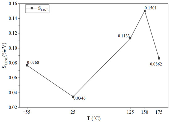
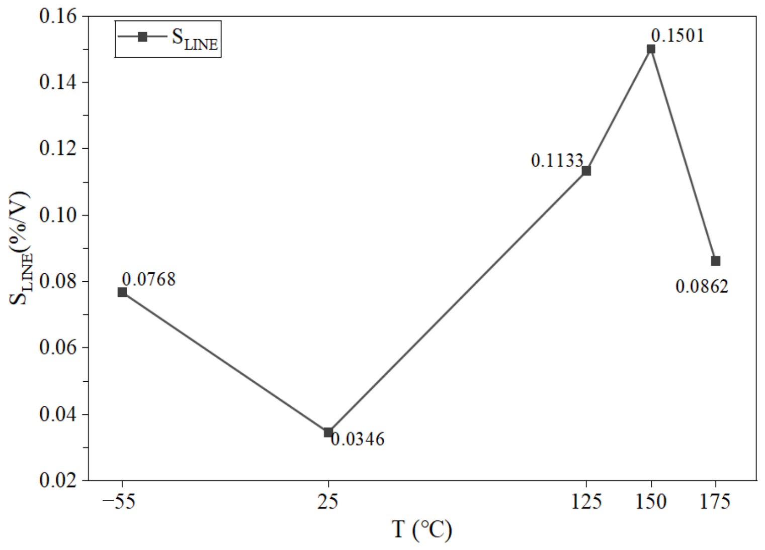
Figure 15 shows the measured line regulation under the conditions of VIN = 3.8–5.5 V, EN = 1.7 V, VOUT = 3.3 V, and ILOAD = 10 mA. At −55 °C, 25 °C, and 175 °C, the line regulation SLINE is 0.0768%/V, 0.0346%/V, and 0.0862%/V, respectively, indicating that the proposed LDO exhibits good input-voltage rejection capability over a wide temperature range.
Figure 15.
Temperature characteristics of line regulation test results.
- C.
- Load regulation
The load regulation is defined as
where ΔVOUT represents the output-voltage variation caused by the load-current change ΔILOAD.
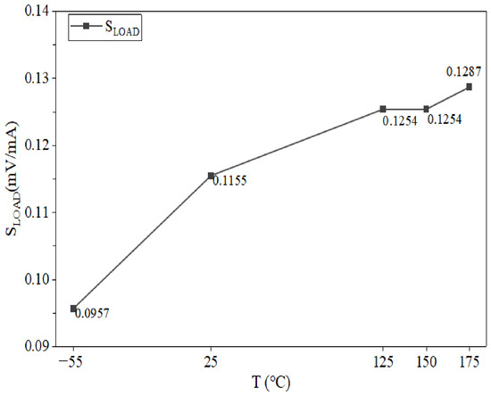
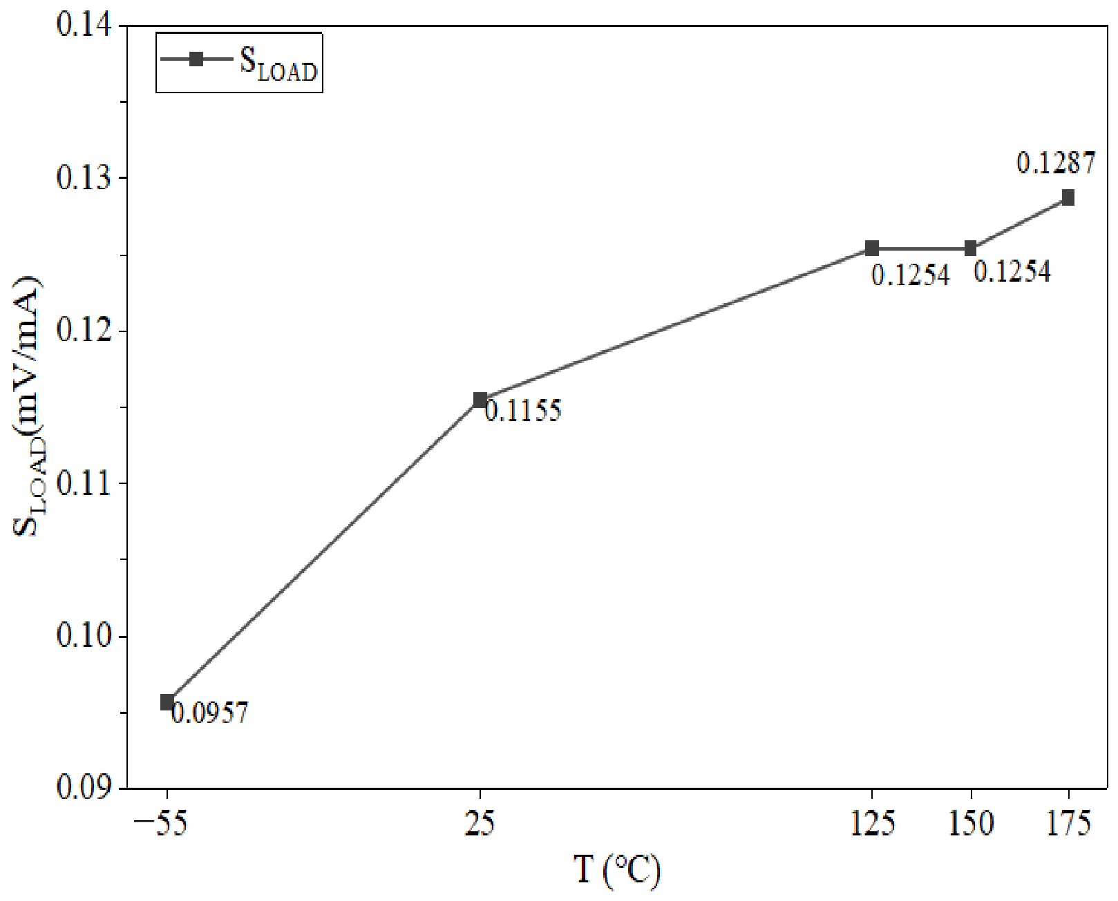
Figure 16 shows the measured load regulation under the conditions of VIN = 3.8 V, EN = 1.7 V, VOUT = 3.3 V, and ILOAD = 1–400 mA. At −55 °C, 25 °C, and 175 °C, the load regulation SLOAD is 0.0957 mV/mA, 0.1155 mV/mA, and 0.1287 mV/mA, respectively. The results indicate that the load regulation remains at a low level over a wide temperature range, demonstrating that the proposed LDO has good suppression capability against load current variations and exhibits excellent load regulation performance.
Figure 16.
Temperature characteristics of load regulation test results.
- D.
- Temperature coefficient
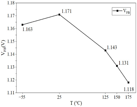
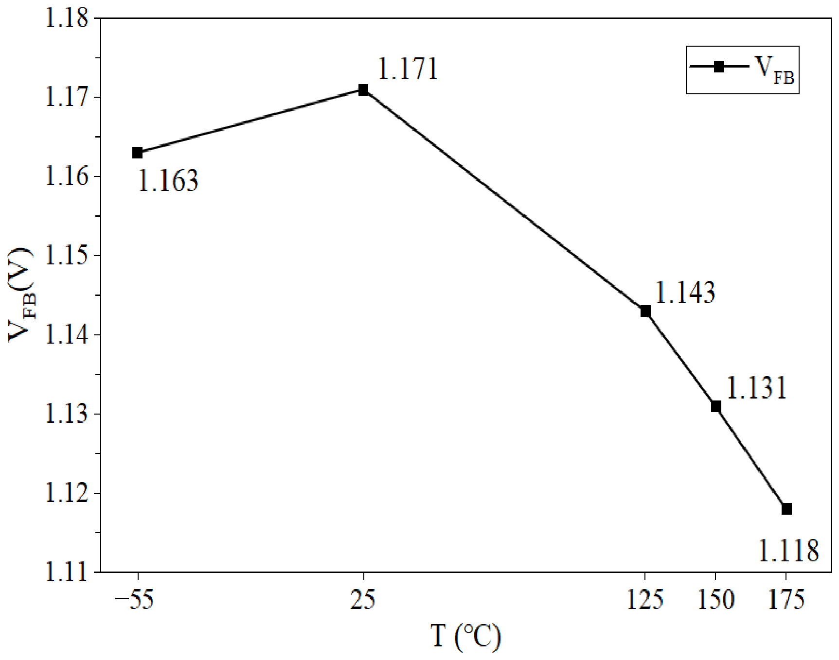
The feedback voltage VFB is measured over temperature to evaluate the temperature characteristics of the chip output voltage under the conditions of VIN = 3.8 V, EN = 1.7 V, VOUT = 3.3 V, and ILOAD = 10 mA. Figure 17 shows the measured VFB versus temperature. The measured VFB values are 1.163 V, 1.171 V, and 1.118 V at −55 °C, 25 °C, and 175 °C, respectively, with a maximum variation of 53 mV.
Figure 17.
Temperature characteristics of the measured feedback voltage VFB.
According to the temperature coefficient formula,
Thus, the temperature coefficient of the feedback voltage is approximately given by
The test results indicate that the feedback voltage exhibits a certain degree of temperature stability over the range from −55 °C to 175 °C, providing a stable reference voltage basis for the LDO’s operation under wide-temperature conditions.
- E.
- Load transient response
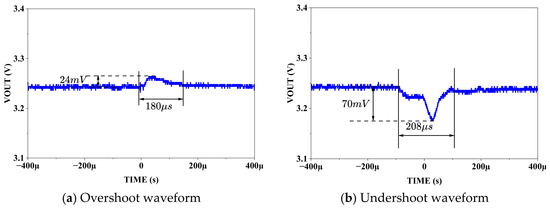
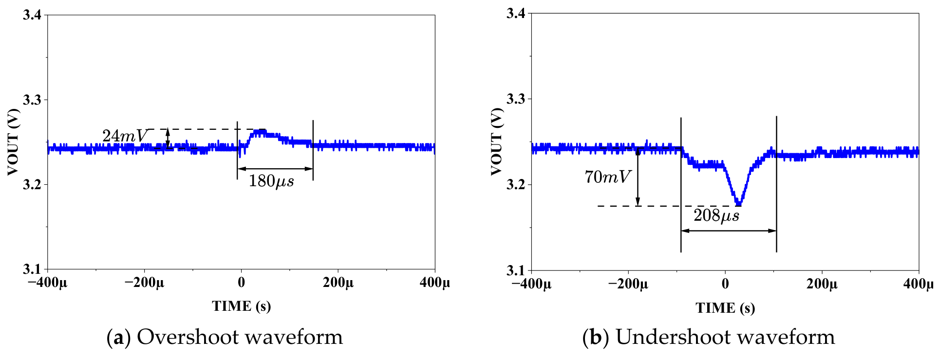
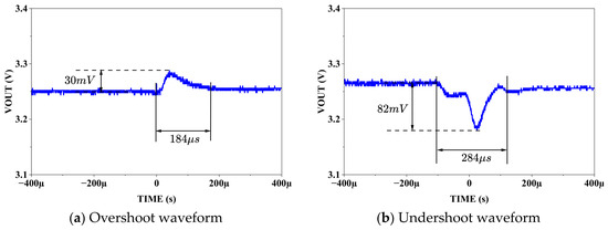
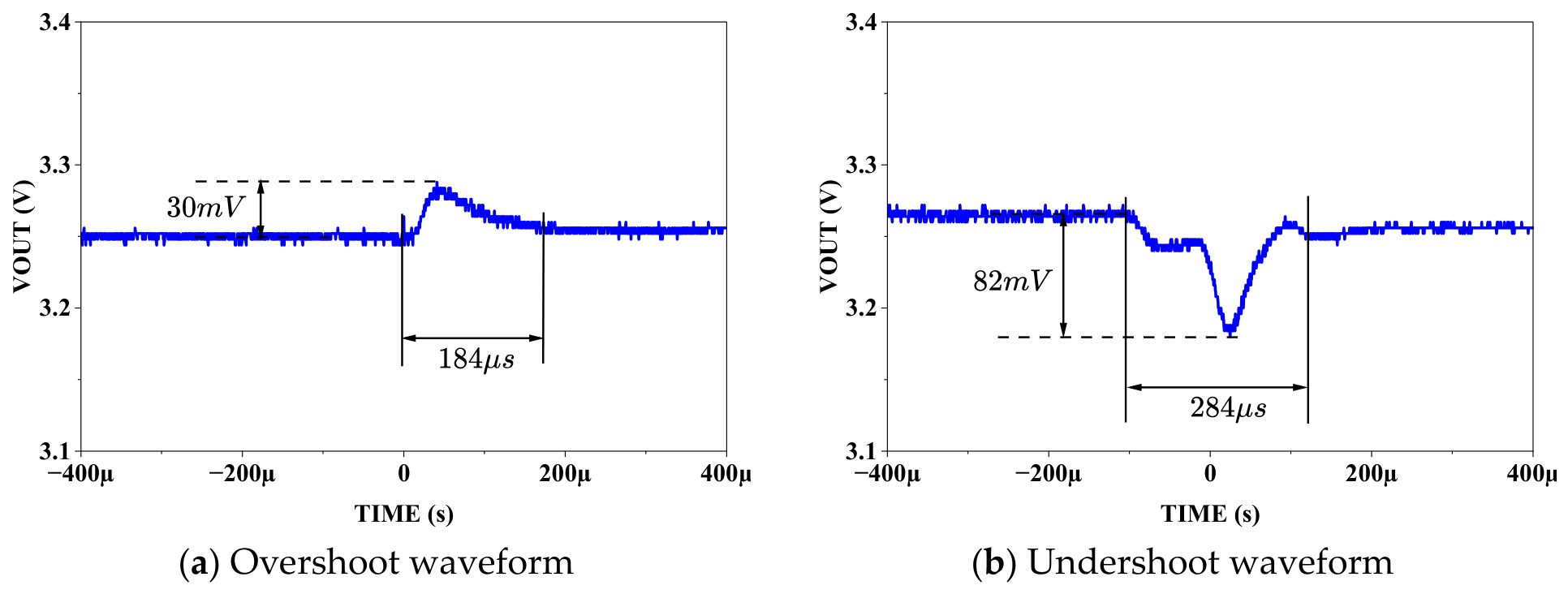
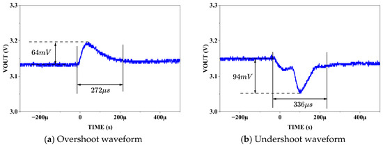
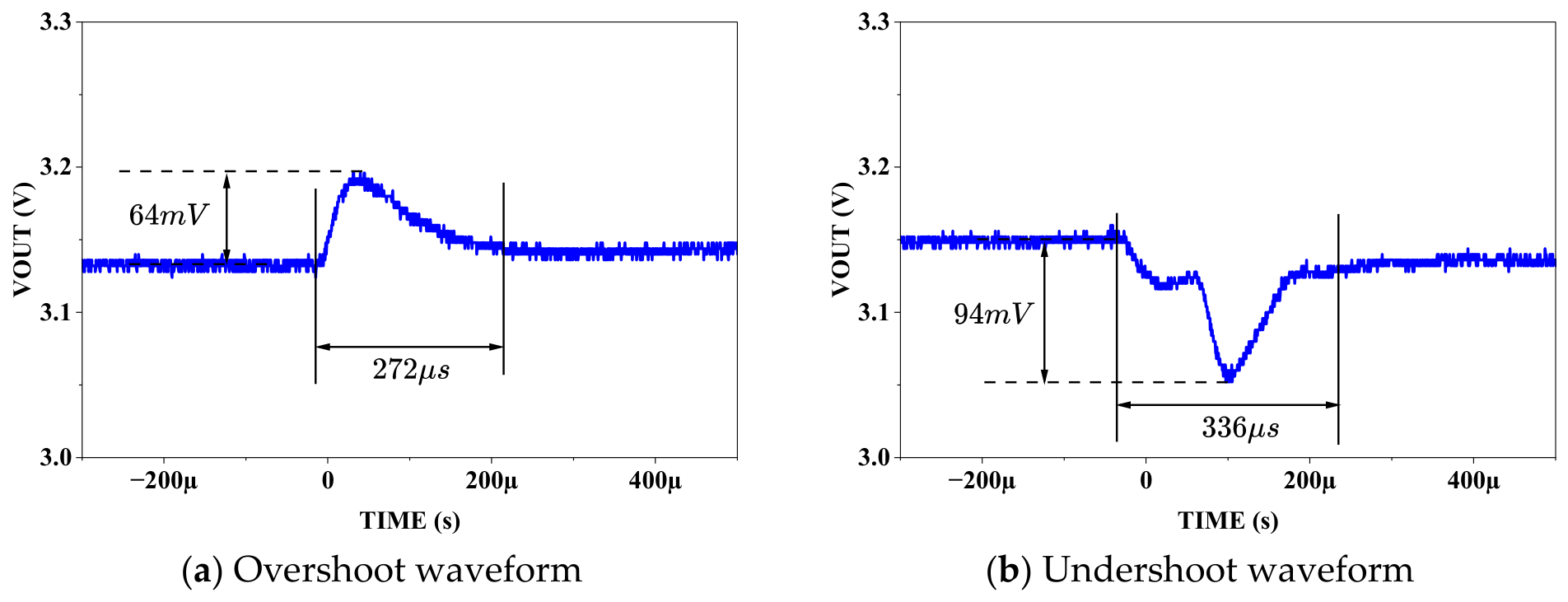
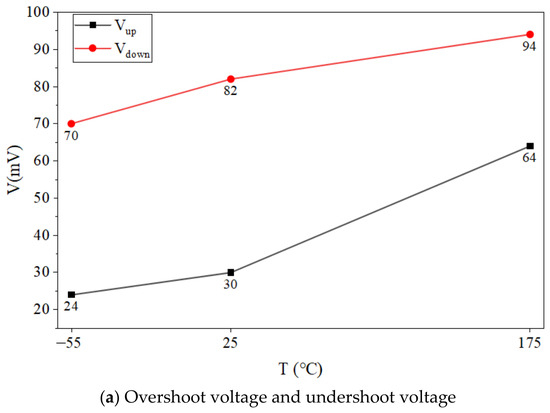
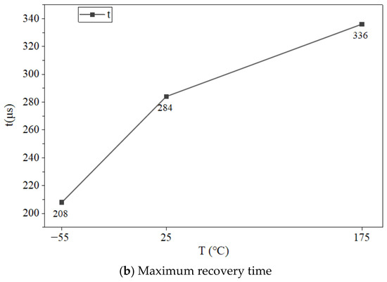
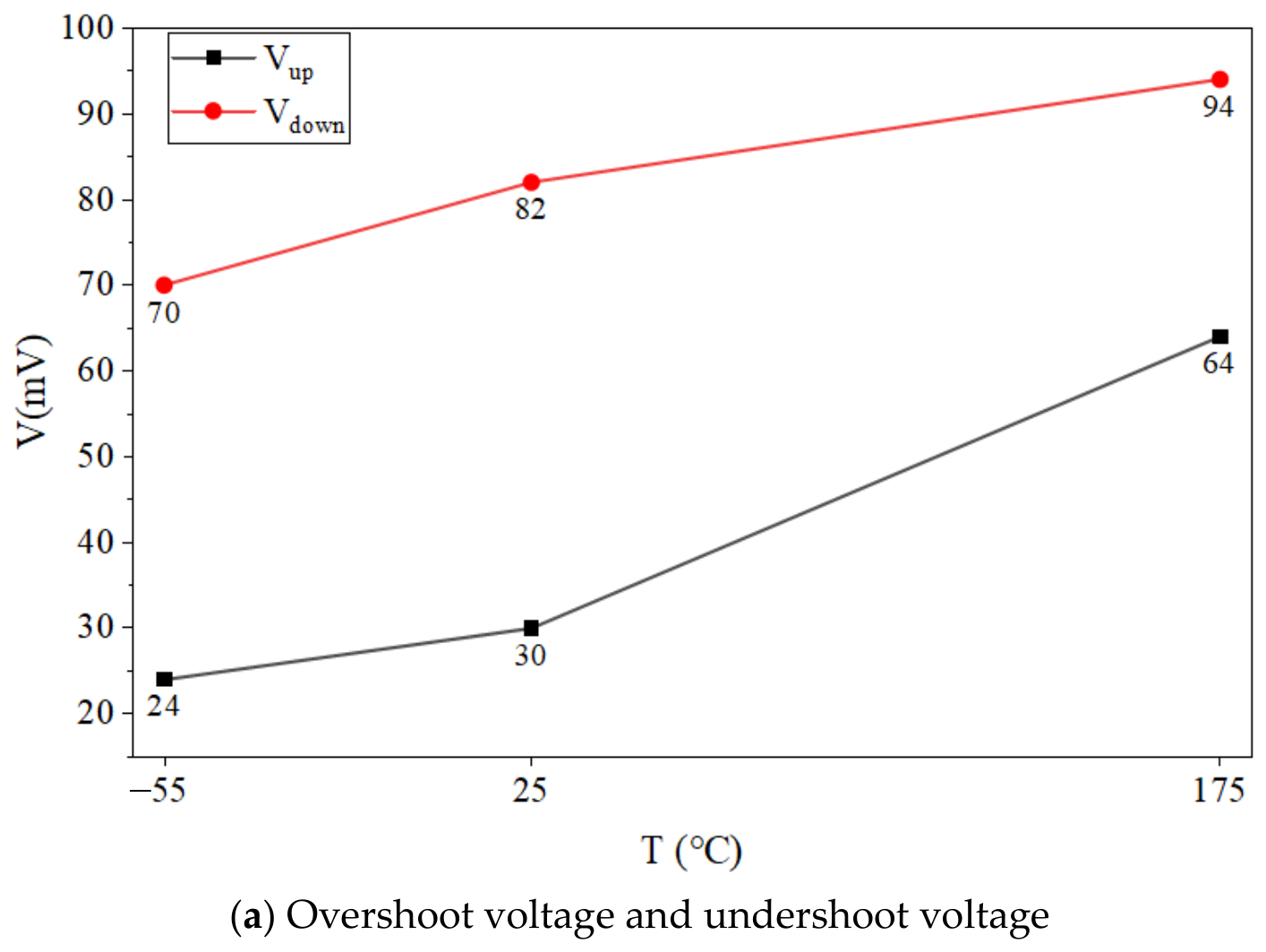
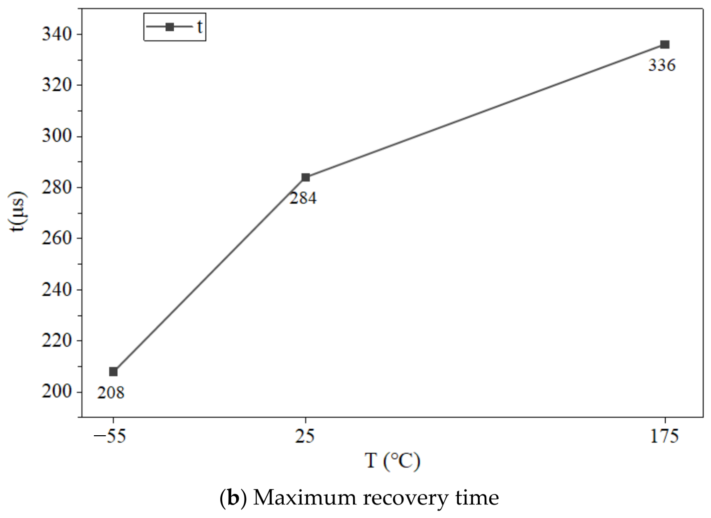
For load transient response characterization, the measurements are performed with EN = 1.7 V, VIN = 3.8 V, VOUT = 3.3 V, and an output capacitor of 0.1 μF. The load-current rising transition (10 mA to 400 mA) and falling transition (400 mA to 10 mA) are measured separately using an electronic load operating in single-transition mode, with a slew rate of 390 mA/μs. Figure 18, Figure 19 and Figure 20 show the load transient response test results of the LDO at different temperatures. Figure 21 further summarizes the variations in output overshoot voltage, undershoot voltage, and maximum recovery time with temperature.
Figure 18.
Load transient response test results (T = −55 °C).
Figure 19.
Load transient response test results (T = 25 °C).
Figure 20.
Load transient response test results (T = 175 °C).
Figure 21.
Temperature characteristics of load transient response test results.
The test results show that, at −55 °C, 25 °C, and 175 °C, the output overshoot voltages are 24 mV, 30 mV, and 64 mV, respectively, while the output undershoot voltages are 70 mV, 82 mV, and 94 mV, respectively. The corresponding maximum recovery times are 208 μs, 284 μs, and 336 μs, respectively.
- F.
- Power supply rejection ratio
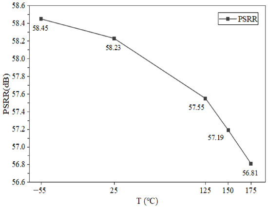
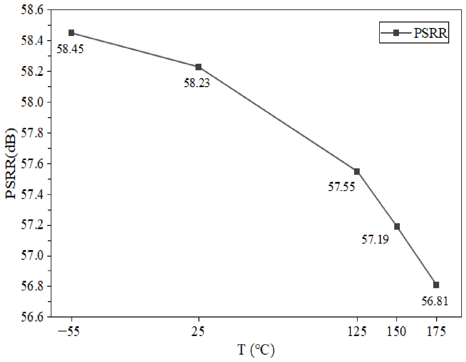
Figure 22 shows the measured power supply rejection ratio (PSRR) at 100 Hz under the conditions of VIN = 3.8 V, EN = 1.7 V, VOUT = 3.3 V, and ILOAD = 400 mA. The measured PSRR values at −55 °C, 25 °C, and 175 °C are 58.45 dB, 58.23 dB, and 56.81 dB, respectively, indicating that the proposed LDO maintains good supply-noise suppression capability over the entire operating temperature range.
Figure 22.
Temperature characteristics of PSRR test results.
4.3. Comparison of Key Performance Metrics
To further verify the high-temperature performance and fast transient response capability of the proposed LDO, five previously reported LDOs are selected for comparison, and the results are shown in Table 1.
Table 1.
Comparison of LDO performance parameters.
Compared with Reference [11], although the transient recovery time of this work is slightly longer, it shows significant advantages in suppressing overshoot and undershoot. The overshoot and undershoot voltages are reduced to 64 mV and 94 mV, respectively, which are much lower than 186 mV and 480 mV reported in [11]. This indicates that the proposed design exhibits better output stability and smaller voltage fluctuations during load transients, effectively reducing interference to downstream sensitive analog/digital circuits.
Compared with References [16] and [17], the proposed LDO demonstrates superior overall performance in terms of maximum load current and transient recovery capability. In particular, the maximum load current of the proposed design reaches 400 mA, which is significantly higher than 200 mA in [16] and 50 mA in [17]. Meanwhile, the recovery time is reduced to 336 μs at 175 °C, indicating that the proposed architecture exhibits stronger load driving capability and faster dynamic regulation, making it more suitable for high-current and highly dynamic load applications.
Compared with References [18] and [19], the proposed LDO achieves higher load current capability while maintaining relatively low transient variations. In particular, compared with the only 10 mA output capability in [19], the proposed design provides a 400 mA load current, representing a significant improvement. In addition, the proposed LDO is verified over a wide temperature range of −55 °C to 175 °C, which is considerably broader than most existing low-dropout regulator designs, demonstrating excellent high-temperature adaptability and environmental robustness, making it more suitable for high-temperature industrial and harsh environment applications.
Overall, the proposed LDO achieves a good trade-off among high load driving capability, output stability, and wide temperature adaptability, demonstrating strong practical engineering value.
5. Conclusions
This work presents a fast-response low-dropout (LDO) linear regulator based on a 0.18 μm SOI process, targeting high-temperature applications such as automotive electronics, aerospace systems, and industrial control. The test results show that the LDO chip has an area of 2840 μm × 1490 μm, with an input voltage range of 3–5.5 V and an output voltage range of 1.2–3.3 V. It can deliver a maximum load current of 400 mA and operates over a temperature range of −55 °C to 175 °C. At 175 °C, the dropout voltage is 255.27 mV, the line regulation is 0.0862%/V, and the load regulation is 0.1287 mV/mA. The overshoot and undershoot voltages are 64 mV and 94 mV, respectively, and the maximum recovery time is 336 μs. At a frequency of 100 Hz, the PSRR remains at 56.8 dB.
These results demonstrate that the proposed LDO achieves good overall performance in terms of high-temperature adaptability, load driving capability, and transient voltage suppression, making it suitable for power management applications requiring high stability and fast response in harsh environments.
Author Contributions
Conceptualization, Y.H. and C.C.; software simulation and parameter optimization, C.Z. and M.Y.F.; data processing, Q.G., C.C. and S.L.; writing—original draft preparation, C.Z.; writing—review and editing, C.C. and Y.H.; supervision, Y.H. All authors have read and agreed to the published version of the manuscript.
Funding
This research was funded by National Natural Science Foundation of China (62471028).
Data Availability Statement
The original contributions presented in this study are included in the article. Further inquiries can be directed to the corresponding author.
Conflicts of Interest
The authors declare no conflicts of interest. The funders had no role in the design of the study; in the collection, analyses, or interpretation of data; in the writing of the manuscript; or in the decision to publish the results.
Correction Statement
This article has been republished with a minor correction to the Author Contributions. This change does not affect the scientific content of the article.
References
- Petrosyants, K.O.; Lebedev, S.V.; Sambursky, L.M.; Stakhin, V.G.; Kharitonov, I.A. Temperature characterization of small-scale SOI MOSFETs in the extended range (to 300 °C). In 2016 22nd International Workshop on Thermal Investigations of ICs and Systems (THERMINIC); IEEE: Piscataway, NJ, USA, 2016; pp. 250–254. [Google Scholar]
- Petrosyants, K.O.; Lebedev, S.V.; Sambursky, L.M.; Stakhin, V.G.; Kharitonov, I.A.; Ismail-zade, M.R.; Ignatov, P.V. High temperature submicron SOI CMOS technology characterization for analog and digital applications up to 300 °C. In 2017 33rd Thermal Measurement, Modeling & Management Symposium (SEMI-THERM); IEEE: Piscataway, NJ, USA, 2017; pp. 229–234. [Google Scholar]
- Grella, K.; Dreiner, S.; Schmidt, A.; Heiermann, W.; Kappert, H.; Vogt, H.; Paschen, U. High temperature characterization up to 450 C of MOSFETs and basic circuits realized in a silicon-on-insulator (SOI) CMOS technology. J. Microelectron. Electron. Packag. 2013, 10, 67–72. [Google Scholar]
- Kappert, H.; Dreiner, S.; Dittrich, D.; Grella, K.; Kelberer, A.; Klusmann, M.; Kordas, N.; Kosfeld, A.; Schmidt, A.; Paschen, U.; et al. High temperature 0.35 micron silicon-on-insulator CMOS technology. Addit. Pap. Present. 2014, 2014, 000154–000158. [Google Scholar]
- Flandre, D.; Terao, A.; Francis, P.; Gentinne, B.; Colinge, J.P. Demonstration of the potential of accumulation-mode MOS transistors on SOI substrates for high-temperature operation (150–300 degrees C). IEEE Electron Device Lett. 2002, 14, 10–12. [Google Scholar]
- Kilchytska, V.; Vancaillie, L.; De Meyer, K.; Flandre, D. MOSFETs scaling down: Advantages and disadvantages for high temperature applications. In Science and Technology of Semiconductor-on-Insulator Structures and Devices Operating in a Harsh Environment: Proceedings of the NATO Advanced Research Workshop on Science and Technology of Semiconductor-on-Insulator Structures and Devices Operating in a Harsh Environment, Kiev, Ukraine, 26–30 April 2004; Springer: Dordrecht, The Netherlands, 2005; pp. 185–190. [Google Scholar]
- Schmidt, A.; Kappert, H.; Kokozinski, R. Enhanced high temperature performance of PD-SOI MOSFETs in analog circuits using reverse body biasing. Addit. Pap. Present. 2013, 2013, 000122–000133. [Google Scholar] [CrossRef] [Scilit]
- Ho, E.N.Y.; Mok, P.K.T. A capacitor-less CMOS active feedback low-dropout regulator with slew-rate enhancement for portable on-chip application. IEEE Trans. Circuits Syst. II Express Briefs 2010, 57, 80–84. [Google Scholar]
- Nasrollahpour, M.; Hamedi-Hagh, S.; Bastan, Y.; Amiri, P. ECP technique based capacitor-less LDO with high PSRR at low frequencies, −89 dB PSRR at 1 MHz and enhanced transient response. In 2017 14th International Conference on Synthesis, Modeling, Analysis and Simulation Methods and Applications to Circuit Design (SMACD); IEEE: Piscataway, NJ, USA, 2017; pp. 1–4. [Google Scholar]
- Ahmadi, M.; Ebrahimi, E. Double-OTA External Capless Low-power LDO Regulator with Enhanced PSR and Transient Response. In 2023 5th Iranian International Conference on Microelectronics (IICM); IEEE: Piscataway, NJ, USA, 2023; pp. 11–15. [Google Scholar]
- Baik, E.; Park, H.J.; Hong, S.W. A Capacitor-less LDO for Mobile Devices with Fast Transient Using High Gain Positive Feedback Loop. In 2023 20th International SoC Design Conference (ISOCC); IEEE: Piscataway, NJ, USA, 2023; pp. 189–190. [Google Scholar]
- Li, H.; Zhan, C.; Zhang, N. A fully on-chip digitally assisted LDO regulator with improved regulation and transient responses. IEEE Trans. Circuits Syst. Regul. Pap. 2018, 65, 4027–4034. [Google Scholar] [CrossRef] [Scilit]
- Ballo, A.; Grasso, A.D.; Palumbo, G. Very-low-voltage charge pump topologies for IoT applications. IEEE Trans. Circuits Syst. Regul. Pap. 2023, 70, 2283–2292. [Google Scholar]
- Dickson, J.F. On-chip high-voltage generation in MNOS integrated circuits using an improved voltage multiplier technique. IEEE J. Solid-State Circuits 1976, 11, 374–378. [Google Scholar]
- Ballo, A.; Grasso, A.D.; Palumbo, G. The Dickson charge pump as a signal amplifier. IEEE Trans. Circuits Syst. Regul. Pap. 2022, 69, 3476–3489. [Google Scholar] [CrossRef] [Scilit]
- Chen, J.J.; Lin, M.S.; Lin, H.C.; Hwang, Y.S. Sub-1V capacitor-free low-power-consumption LDO with digital controlled loop. In APCCAS 2008—2008 IEEE Asia Pacific Conference on Circuits and Systems; IEEE: Piscataway, NJ, USA, 2008; pp. 526–529. [Google Scholar]
- Hwang, Y.S.; Lin, M.S.; Hwang, B.H.; Chen, J.J. A 0.35 μm CMOS sub-1V low-quiescent-current low-dropout regulator. In 2008 IEEE Asian Solid-State Circuits Conference; IEEE: Piscataway, NJ, USA, 2008; pp. 153–156. [Google Scholar]
- Jeon, I.; Guo, T.; Roh, J. 300 mA LDO using 0.94 μA I Q with an additional feedback path for buffer turn-off under light-load conditions. IEEE Access 2021, 9, 51784–51792. [Google Scholar]
- Gweon, S.; Lee, J.; Kim, K.; Yoo, H.J. 93.8% current efficiency and 0.672 ns transient response reconfigurable LDO for wireless sensor network systems. In 2019 IEEE International Symposium on Circuits and Systems (ISCAS); IEEE: Piscataway, NJ, USA, 2019; pp. 1–5. [Google Scholar]

Disclaimer/Publisher’s Note: The statements, opinions and data contained in all publications are solely those of the individual author(s) and contributor(s) and not of MDPI and/or the editor(s). MDPI and/or the editor(s) disclaim responsibility for any injury to people or property resulting from any ideas, methods, instructions or products referred to in the content. |
© 2026 by the authors. Licensee MDPI, Basel, Switzerland. This article is an open access article distributed under the terms and conditions of the Creative Commons Attribution (CC BY) license.