


Abstract
Silicon carbide (SiC) is the leading wide-bandgap semiconductor material, providing mature doping and device fabrication. Additionally, SiC hosts a multitude of optically active point defects (color centers) and is relevant for many applications in quantum technologies. A crucial step towards harnessing the full potential of the SiC platform includes technologies to create color centers with defined localization and density, e.g., to facilitate their coupling to nano-photonic structures and to observe cooperative effects. Here, silicon vacancy centers and divacancies stand out, as no impurity atom is needed, and high-thermal budget annealing steps can be avoided. We characterize the effect of localized, femtosecond laser irradiation of SiC, investigating surface modifications and photoluminescence, including Raman spectroscopy and optical lifetime measurements. We employ commercial, high-purity, semi-insulating substrates and an industrial-grade laser system to explore broader applicability of the method. As a novel approach, we apply femtosecond laser irradiation to SiC substrates with an epitaxial graphene layer and find that the threshold for photoluminescence due to laser treatment is lowered.
1. Introduction
Silicon carbide (SiC) has seen tremendous improvements as a semiconductor platform in recent years, especially in terms of crystal quality and wafer sizes that can now reach up to 8 inches. Together with these improvements, it has also been established as a host material for single color centers and their applications in quantum technologies. Silicon vacancy centers () have several favorable characteristics for applications in quantum technologies [1,2]. They have been studied in several polytypes, most notably in 4H-SiC and 6H-SiC with different configurations in both polytypes [3,4,5]. In 4H-SiC, they exist in two different configurations [3] corresponding to a missing silicon atom at a cubic and a hexagonal lattice site. The defects show zero phonon lines at 861 nm for V1 (cubic) and 916 nm for V2 (hexagonal) [6,7]. Moreover, do provide an optically readable ground-state spin with a zero field splitting of 4.5 MHz for V1 and 70 MHz for V2 [6,8], which is addressable with standard RF components. However, the contrast of this optically detected magnetic resonance (ODMR) is comparably low (a few %). An additional challenge is the fact that luminescence is hard to collect in (0001) SiC, because of the dipole orientation in the SiC lattice. (0001) material is however the material with the highest commercial availability. Milestones include super-radiance [9] from two color centers, near-transform limited emission even in photonic nanostructures [10] as well as magnetic sensors working under extremely harsh conditions like high pressure [11]. SiC has also emerged as a promising platform for epitaxial graphene growth by sublimation of SiC, enabling the straightforward fabrication of large area, high quality graphene directly on a semiconducting substrate with different polytypes such as 6H-SiC [12,13,14], 4H-SiC and 3C-SiC [15,16,17]. Due to its high carrier mobility [18] graphene has many possible applications in various fields [19], such as high frequency transistors [20], photonics [21,22] and also with as transparent electrodes for Stark shift tuning of quantum systems [15].
Localized have been created by various techniques: ion implantation (focused ion beams [23] or implantation through a mask [24]) or laser writing in both 4H-SiC and 6H-SiC [25,26,27,28,29]. Ion-based techniques in principle allow for the highest precision in localization which has been shown to be mainly limited by the straggle of the ions to tens of nanometers for keV ion implantation [30]. However, they also create high levels of damage and potential additional defects and require costly equipment. Laser writing has been investigated as an alternative that relies on highly non-linear processes. Previous works suggest the involvement of 16 photons in the generation of a vacancy defect in SiC [25]. With such an extremely non-linear process, even an optical technology allows for precise localization that has been estimated to be as good as 80 nm [25]. Femtosecond lasers can also be used to manufacture photonic structures directly into SiC with the most recent example being the use of hollow cylindrical vector beams to produce solid immersion lenses to enhance fluorescence [31].
To address different applications in quantum technologies, not only controlling the spatial placement but also varying the density of color centers is crucial: whereas single photon sources naturally require using a single color center; higher density ensembles can be favorable for highly-sensitive magnetic sensors based on optically-readable spins. In this case, higher defect density enables brighter fluorescence and thus reduces photon shot noise in the optical read-out. Moreover, enhancing defect density in ensembles may allow to observe the transition from uncoupled to collective emission (super-radiance) [32].
Laser writing can be used to create single in 4H-SiC as well as ensembles [25]. However, the creation of dense ensembles requires higher pulse energies that are well above the ablation threshold, leading to increased damages to the crystal [33]. In the context of localized creation of color centers, ablation processes are a parasitic effect and will limit the creation of dense color center ensembles. In this work, we investigate if applicability of laser writing of can be extended: We perform laser processing using a commercial laser structuring system and irradiate a straightforwardly available commercial High Purity Semi-Insulating (HPSI) SiC. We elucidate whether laser processing is compatible with using epitaxial graphene layers that have been suggested as transparent electrode to electrically tune color centers. We here report on the photoluminescence (PL) from localized laser-irradiated areas, and we analyze surface morphology and Raman spectra, as well as PL spectra and lifetimes.
2. Materials and Methods
Sample Pre-Treatment
A 4-inch (0001) oriented HPSI 4H-SiC wafer purchased from Wolfspeed, Inc. (Durham, NC, USA) was diced into quadratic chips of <10 × 10 mm2. We chose 4H-SiC because in this material possesses promising properties and the polytype is readily commercially available. Diced chips were then solvent-cleaned with acetone and isopropanol to remove the protective resistant layer applied for dicing. Surfaces are chemically mechanically polished to a roughness of <0.5 nm according to manufacturer specifications.
On the first sample, an epitaxial graphene layer was grown at 1600 °C [14]. The second sample was annealed in a vacuum (5.5 × hPa) at 800 °C for 3 h. Annealing at temperatures above 600 °C has been found to reduce the concentration of [24,34] where ab initio calculations show that migrate and recombine to form pairs of antisite vacancy () [35,36]. We note that none of these pre-treatment is expected to hinder the creation of .
3. Results
3.1. Irradiation of HPSI SiC with Graphene Layer
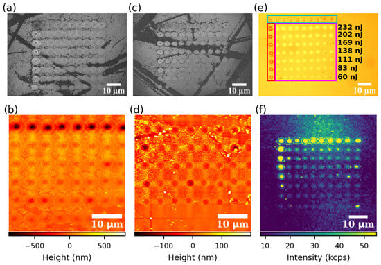
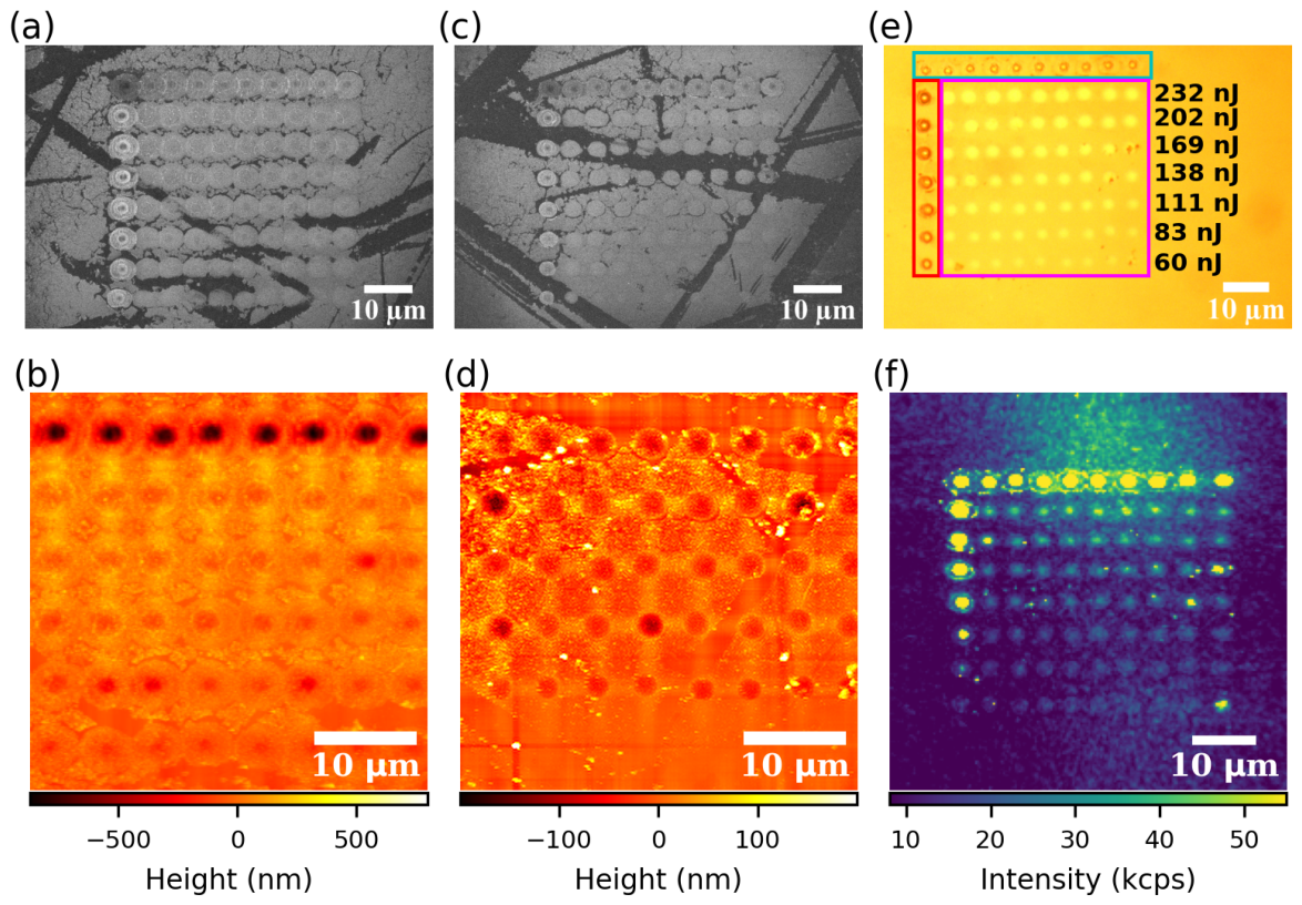
We irradiated the 4H-SiC samples using an industrial-grade laser structuring system (BlueCut, Menlo Systems GmbH, Martinsried, Germany) operating at a wavelength of 1030 nm, with a pulse duration of 383 fs, a repetition rate of up to 1 MHz, and a maximum pulse energy of 10 µJ. For all experiments, the repetition rate was set to 10 kHz. The laser beam, which was linearly polarized, was focused using a Thorlabs LMH-20X-1064 objective (NA = 0.4), resulting in a calculated beam diameter of 2.4 m () in air. After laser processing, the samples were cleaned in acetone using an ultrasonic bath to remove particles collected on the surface during processing. The laser-written patterns labeled pattern 1 and 2 were imaged using a commercial scanning electron microscope (SEM, SU8000, Hitachi, Tokyo, Japan) in Figure 1a,c, and with a white-light optical microscope in Figure 1e, corresponding to the pattern 2 shown in Figure 1c. The top row and the leftmost column serve as markers, on pattern 1 we used 5 pulses per spot at 522 nJ on Figure 1a (232 nJ on Figure 1c for pattern 2), and 10 pulses per spot with pulse energy ranging from 232 nJ to 522 nJ on Figure 1a for pattern 1 (60 nJ to 232 nJ on Figure 1c for pattern 2) for the leftmost column to induce a clear surface modification. The rows of spots visible within this marker angle were processed using a single pulse of the laser with pulse energies ranging from 232 nJ to 522 nJ on Figure 1a for pattern 1 (60 nJ to 232 nJ on Figure 1c for pattern 2). This preliminary investigation by SEM and white-light microscopy already indicates a challenge in laser writing of (dense) color center ensembles: In the regions where multiple pulses have been used for processing, around the laser processed area a structure occurs that is due to laser ablation and re-deposition of material. This re-deposited material however will not be of high quality and is typically observed to be amorphous [27].
Figure 1.
(a,c) SEM images at 5 kV of laser-written patterns 1 and 2 on the HPSI 4H-SiC sample with a graphene layer, with pulse energy ranging from 232–522 nJ (pattern 1) on (a) and 60–232 nJ (pattern 2) on (c). (b,d) respective AFM measurements of the patterns in (a,c). (e) White-light optical microscope image of the laser-written pattern 2 on the sample with graphene with higher pulse energy on the top row (232 nJ) and lower pulse energy on the bottom row (60 nJ). Spots in the leftmost column (red box) were written using trains of 10 pulses at the energy corresponding to each row. Spots in the top row (cyan box) were written using trains of 5 pulses at 232 nJ, while spots in between (pink box) were written using single pulses at the energy corresponding to each row. (f) Associated confocal PL map of the laser-written pattern on (c,e).
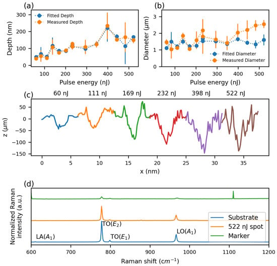
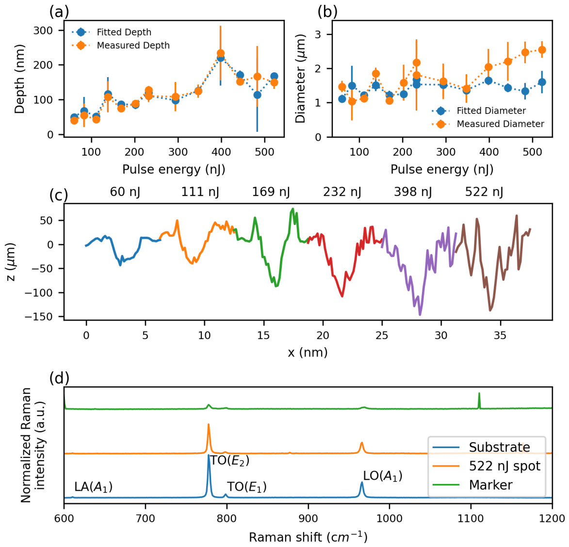
We assume based on imaging of bare 4H-SiC surface that light gray areas in Figure 1a,c are graphene while darker parts are attributed to be the bare 4H-SiC surface. In darker areas, graphene on the surface appears to be removed, likely occurring during laser processing when ablated material was ejected scratching the surface. Additional damage may have occurred during sample handling. Although laser-written spots exhibit a contrast similar to that of the surrounding graphene layer, this does not necessarily indicate that graphene remains at these sites, as all pulse energies used are well above the ablation threshold of graphene [37,38]. Instead, their higher brightness compared to the bare substrate may arise from surface modification/ablation of 4H-SiC induced by laser pulses, as observed in femtosecond laser ablation of 4H-SiC studies [39,40]. To further study surface modifications on the graphene and 4H-SiC, atomic force microscope (AFM) measurements were performed on both patterns 1 and 2 using a commercial AFM (XE-70, Park Systems, Gwacheon, Republic of Korea). AFM images are shown in Figure 1b,d which are associated to laser-written patterns 1 and 2 in Figure 1a,c. The femtosecond laser pulses created craters on the 4H-SiC surface as observed in the literature [26]. Figure 2a,b show the depth and full width at half maximum (FWHM) of the laser-written craters, measured directly from the AFM topography. The local surface level was defined as the median height of the pixels surrounding each crater. Crater depth was then determined as the difference between this surface level and the 1st percentile of the deepest points within the crater, reducing the influence of isolated noisy pixels. The crater width was obtained by extracting a line profile through the deepest measured point in the crater and calculating the distance between the two intersections of the profile with the half-depth level. Example crater profiles are plotted on Figure 2c for different pulse energies ranging from 60 nJ to 522 nJ. We measure between 3 to 8 clearly discernible craters per pulse energy. For each measured crater, a Gaussian fit was performed to approximate its shape. We observe as a trend the crater depth increased with pulse energy, and the depths obtained from the Gaussian fits closely matched the directly measured values. At 398 nJ, however, a large spread in the measured depths resulted in an apparent increase above the general trend. In contrast, the diameters of the craters do not show a clear increase with pulse energy up to 350 nJ, but rather remain approximately constant, with a mean measured value of (1.77 ± 0.50 m). The diameters obtained from the Gaussian fits are slightly smaller on average, with a mean value of (1.42 ± 0.17 m). Both values are close to the FWHM of the femtosecond laser focus (1.41 m), which is consistent with the lateral extent of the modification being governed primarily by the focal spot size. However, fitted diameters are not as accurate as for the depth especially for energies above 350 nJ where they diverge, most probably because of the rough surface within the crater.
Figure 2.
(a,b) Mean depth and width (FWHM) of the laser-written spots on the HPSI 4H-SiC sample with a graphene layer as a function of laser pulse energy. Mean values measured from the AFM topography are shown in orange, while mean values obtained from Gaussian fits are shown in blue. (c) Lateral profiles of laser-written spots taken at deepest measured points for different pulse energies ranging from 60 nJ to 522 nJ. (d) Raman spectra of the unprocessed HPSI 4H-SiC with graphene, a spot irradiated using a 522 nJ pulse and a marker. Spectra are offset vertically for clarity.
Figure 2d shows Raman spectra taken in a home-built confocal laser-scanning fluorescence microscope (CLSM), labeled CLSM 1. In CLSM 1, the sample was cooled down to 4.3 K in a closed-cycle cryostat (CRYOVAC GmbH & Co. KG, Troisdorf, Germany). In CLSM 1, we excite the SiC sample using a tunable titanium sapphire laser (Matisse, Sirah Lasertechnik GmbH, Grevenbroich, Germany) operating at 737.19 nm focused on the sample with a microscope objective (MPLN 100×, NA = 0.9, Olympus, Tokyo, Japan). PL and Raman scattered light is collected using the same objective and reflected laser light is rejected using a 740 nm dichroic mirror.
Transmitted PL is further filtered with a longpass filter and coupled to a single mode fiber that can either be connected to an APD (SPCM-AQRH, Excelitas, Pittsburgh, PA, USA) or a spectrometer (Acton SpectraPro 2750, Princeton Instruments, Trenton, NJ, USA) equipped with a 600 lines per mm grating and a liquid nitrogen cooled CCD camera (Spec10, Princeton Instruments, Trenton, NJ, USA). Measurements were performed on an unprocessed part of the sample, a written spot at 522 nJ and a marker made with a train of 10 pulses at 522 nJ. The Raman lines observed on the substrate are characteristic of 4H-SiC. At a pulse energy of 522 nJ, the laser-written spots exhibit Raman peak intensities that are reduced by 32%, 57%, and 30% for the TO(), TO(), and LO() peaks, respectively, relative to the unprocessed substrate. In contrast, laser writing with a train of 10 pulses produces much more pronounced modifications to the Raman spectrum. The intensities of the TO(), TO() and LO() peaks are reduced by 89%, 60% and 87%, respectively, and all three peaks exhibit broadening. In addition, the LA() peak is no longer visible, indicating severe damage to the crystal lattice. While this Raman spectrum shows no sign of amorphous material even for 522 nJ, the strong decrease in Raman peak intensity has been associated with significant crystal damage in previous work [26]. The Raman spectrum does not show clear evidence for remaining graphene in accordance with the observation of ablation of material at the surface. To further investigate the material composition of the laser-written spots, we performed energy-dispersive X-ray spectroscopy (EDX) measurements using the same SEM instrument. In particular, we searched for oxygen incorporation (oxidation) induced by the laser writing process. EDX measurements were carried out at an accelerating voltage of 20 kV over the entire laser-written pattern on the pristine sample, as well as over patterns 1 and 2 on the sample with graphene. Additional measurements were performed on individual laser-written spots. No oxygen-related peaks were detected in any of the spectra suggesting that oxygen contamination is negligible within the EDX detection limits consequently hinting that no excess oxidation takes place during laser writing.
To investigate room-temperature photoluminescence from the laser processed area, we use another home-built CLSM. We use continuous 785 nm laser light (OBIS LX 785, Coherent, Saxonburg, PA, USA) for excitation. In addition, we use a tunable, pulsed super-continuum laser source with typical pulse width < 100 ps (NKT Super K-Extreme, Birkerød, Denmark) to measure the excited state lifetime of the observed PL. In both cases, we use a 100× microscope objective with 0.9 NA (EC EPN 100×/0.9, Carl Zeiss Microscopy GmbH, Oberkochen, Germany DIC) to focus the laser onto the sample and to collect PL in a reflection geometry. We separate PL and reflected laser light using a 785 nm edge dichroic mirror (Laser-Beamsplitter HC R785 lambda/5 PV flat, Semrock, Rochester, NY, USA). We detect PL using silicon avalanche photo-diodes (APDs) for spectrally-integrated detection (SPCM-AQRH-14, Excelitas, Pittsburgh, PA, USA). Alternatively, we sent the PL to a spectrometer equipped with a silicon CCD (Acton Standard SP-2558 Spectrometer with Pixis 256E CCD, Princeton Instruments, Trenton, NJ, USA). In both cases, we use a 850 nm long pass filter for additional laser filtering. Figure 1f shows a room temperature confocal PL map of pattern 2 depicted in Figure 1c. Localized PL is visible resembling the regular array that was processed by irradiating the SiC sample with single laser pulses, however, a significant level of PL also originates from areas not irradiated by the laser due to already present native defects remaining in our substrate, the PL ratio between the written spots at 60 nJ (bottom-most row) with the background is only ~2.
3.2. Irradiation of Pristine HPSI SiC
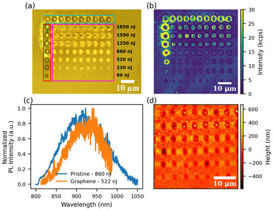
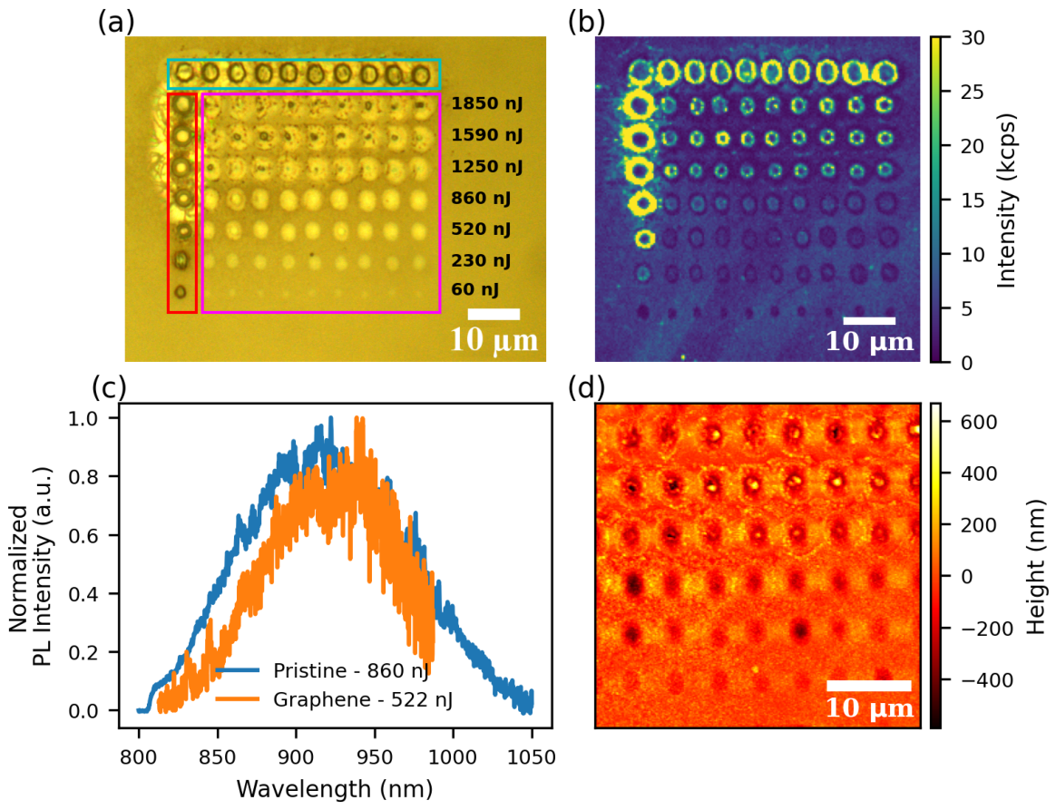
As a reference, we processed a pristine HPSI 4H-SiC substrate following the same method described in the previous section, except that the alignment markers were written using a repetition rate of 100 kHz. We wrote a pattern on the surface with pulse energies ranging from 60 nJ (bottom row) to 1850 nJ (top row). Figure 3a shows a white-light optical microscope image of the resulting pattern. Figure 3b shows a confocal PL map of the laser processed area. The bottom-most row has been exposed to 60 nJ laser pulses; here, PL intensity is even slightly reduced compared to the surrounding, unprocessed SiC. This could be attributed to local annealing [41] and surface modification as our 60 nJ pulses have energies above the reported modification threshold [39] but below the ablation threshold [40] necessary to create vacancies. Ref. [25] identifies the process that creates in SiC as highly non-linear. According to Ref. [25], 16 photons at a wavelength of 790 nm are involved in creating a single defect. For such a highly non-linear process (among other parameters), the peak intensity of the laser pulse will be crucial. We thus compare the laser and optics parameters in our work to previous work in Table 1. We find a slightly lower threshold than previously reported for the onset of PL on the pristine sample and a strongly reduced threshold for the sample with graphene. This could be explained by the absorptance of graphene which is 2.3% [42] compared to only 0.16% at its surface in 4H-SiC at 1030 nm [43] making it 14 times higher.
Figure 3.
(a) White-light optical microscope image of the laser-processed pattern observed on the surface. The top row and the leftmost column serve as a marker, here we used a train of 5 pulses per spot at 1850 nJ for the top row (cyan box), and 10 pulses per spot with pulse energy ranging from 60 to 1850 nJ for the leftmost column to induce a clear surface modification (red box). The rows of spots visible within this marker angle have been processed using a single pulse of the laser with pulse energies ranging from 60–1850 nJ (pink box). (b) Confocal PL map of the laser-written pattern presented in (a). PL with wavelengths > 850 nm was detected. From top to bottom, the rows have been written with 1850, 1590, 1250, 860, 520, 230 and 60 nJ (single pulse per spot). (c) Exemplary PL spectra from a spot irradiated with 860 nJ on the pristine sample and from a marker irradiated at 522 nJ on the graphene sample. (d) AFM image of the laser-written pattern.
Table 1.
Summary of femtosecond lasers and optics parameter used in this works and for various previous work. is the pulse duration, the pulse energy and the corresponding peak intensity.
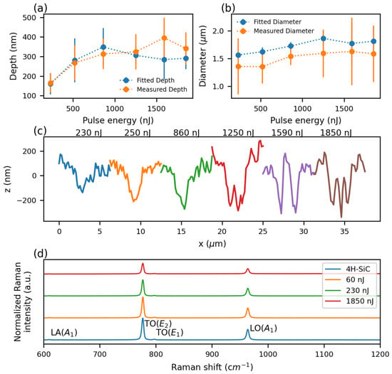
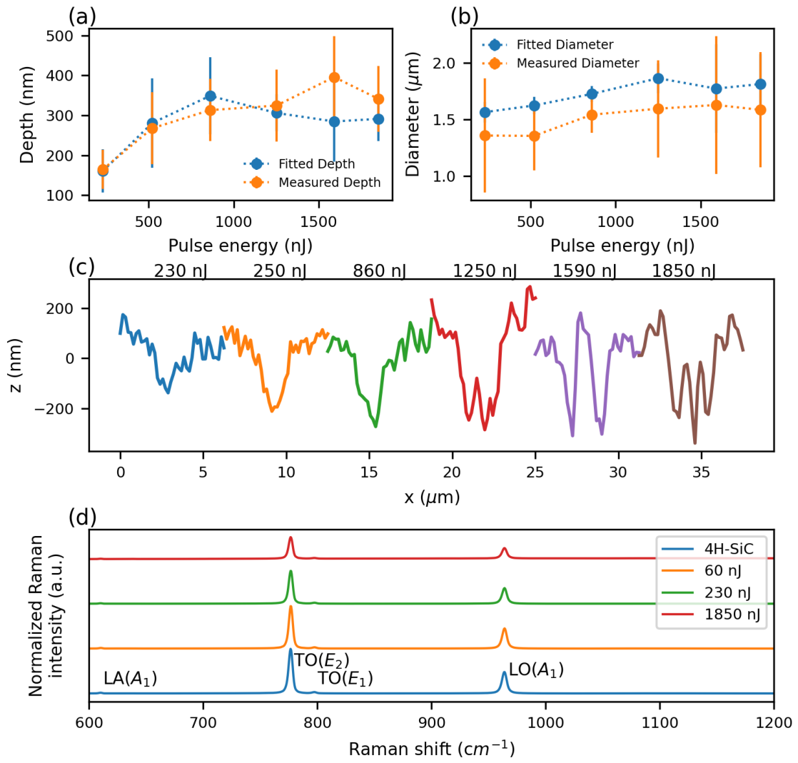
Figure 4d shows Raman spectra taken using a commercial Raman spectrometer (Senterra, Bruker Optik GmbH, Ettlingen, Germany) with a 532 nm excitation laser on the pristine sample from an unprocessed area and from spots written at 60 nJ, 230 nJ and 1850 nJ. Raman spectra taken from dimples made with single pulse at 60 nJ result in reduced Raman peak intensities of 5% for the TO(), TO() and LO() peaks relative to unprocessed 4H-SiC. At 230 nJ, the reduction becomes more pronounced, reaching 26%, 27% and 27% for the TO(), TO() and LO() peaks, respectively. Even larger reductions are observed at 1850 nJ, amounting to 51%, 32% and 50% for the TO(), TO() and LO() peaks, respectively, further indicating significant damage to the crystal lattice. To further analyze the structures, we again employ AFM measurements. The resulting image in Figure 3d shows spots made with single pulses from 230 nJ to 1850 nJ. For the spots irradiated with 60 nJ, a shallow surface modification is visible. For spots written with pulse energy between 230 nJ to 860 nJ ablated material results in a crater-like hole. At higher pulse energy, we find a dimple with a hillock in the middle and ring shaped wall in the outer area. Figure 4a,b summarize the depth and width of the surface structures obtained using the same method described in the previous section.
Figure 4.
(a,b) Mean depth and width (FWHM) of the laser-written spots on the HPSI 4H-SiC sample as a function of laser pulse energy. Mean values measured from the AFM topography are shown in orange, while mean values obtained from Gaussian fits are shown in blue. (c) Lateral profiles of craters taken at deepest measured points for different pulse energies ranging from 230 nJ to 1850 nJ. (d) Raman spectra of the unmodified pristine HPSI 4H-SiC and of spots made at different laser pulse energies of 60 nJ, 230 nJ and 1850 nJ. The spectra are offset vertically for clarity and have been recorded using a 532 nm laser.
As discernible from Figure 4a,b depths grows with pulse energy up to 750 nJ where it starts to reach a plateau around 350 nm. The width slowly increases with pulse energy, reaching 1.58 ± 0.51 m at 1850 nJ, which is comparable to the FWHM of the laser beam’s. The fitted diameters appear to be on average 13% larger than the measured ones. Gaussian fit stops being applicable for pulses above 860 nJ, as shown in Figure 4c, where for higher pulse energies, material at the center of the crater flows back up to the surface because of the extreme temperature and pressure caused by the laser pulse.
We then perform PL spectroscopy of the bright spots created by irradiation with single laser pulses. For all photo-luminescent spots, we obtain typical room temperature spectra, as displayed in Figure 3c. This very broad PL spectrum without a discernible zero-phonon line has been identified as the typical PL signature of at room temperature [7]. We compared them with PL spectra taken on the graphene sample on markers written at 522 nJ. The broad spectrum in the region of interest for is in good agreement. The measured PL intensities and the fact that second order photon correlation measurements on the bright spots show no anti-bunching point to defect ensembles. Room temperature spectra are similar to previous work [26].
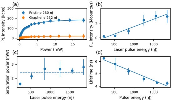
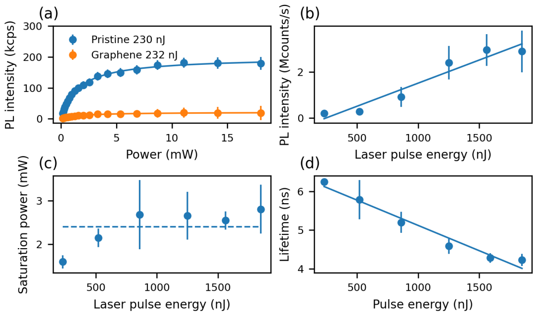
We measure PL saturation curves for each laser irradiated spot (9 per pulse energy) and average over the measurements on the spots irradiated with the same pulse energy. Figure 5a exemplary shows the saturation measurement for spots irradiated with 230 nJ on the pristine sample and 232 nJ on the graphene sample. To correct the data for background, we perform a saturation measurement at a spot 10 m downward from the row written at 60 nJ. We correct the data points by subtracting the background. We note that the PL background also showed a saturation behavior. This might indicate that native point defects contribute to the background as reported previously [44]. Figure 5b shows the saturation count rate as a function of the writing pulse energy. Saturation count rates increase linearly with laser pulse energy indicating a linear increase of luminescent defects with pulse energy assuming a constant emission rate for each created defect. On the other hand, we will below discuss changes on excited state lifetimes that indicate non-radiative processes and thus changes in the emission rates.
Figure 5.
(a) Comparison of mean saturation of PL induced via laser processing on the pristine 4H-SiC and 4H-SiC with a graphene layer of spots written with a 230 nJ and 232 nJ pulse energy for power measured before focusing objective. (b) Mean saturation count rate detecting PL with wavelengths longer than 850 nm in function of laser pulse energy. (c) Mean saturation power associated with the saturation count rate in function of the pulse energy, dashed line shows the mean saturation power at 2.40 mW. (d) Mean lifetime measurements detecting PL with wavelengths longer than 850 nm in function of the pulse energy.
In addition, modifying the surface profile (Figure 4), especially for increased pulse energy, also changes the crystalline properties of SiC in the vicinity of the spots [26,27,45]. When aiming to create , carbon vacancies () are also created nearby due to their low formation energy. Carbon vacancies are not optically active. They provide non-radiative decay paths for therefore quenching their PL [25,46,47]. Figure 5d summarizes the lifetimes extracted from PL measurements (>850 nm). Again, we obtain lifetimes by averaging measurements from all spots irradiated with the same pulse energy. For spots irradiated with 230 nJ pulses, we find ns which matches ns obtained for created using electron irradiation [48], again hinting at the creation of . decreases linearly with pulse energy, indicating quenching by , and also potential interaction with extended defects due to laser irradiation. In contrast, the saturation power as displayed in Figure 5c did not change with pulse energy.
To obtain more information on the defects created by the laser writing process, both samples (graphene and pristine) and a reference HPSI 4H-SiC sample implanted with 350 keV protons at a dose of were cooled down to 4.3 K in the CLSM 1 setup described in the previous section.
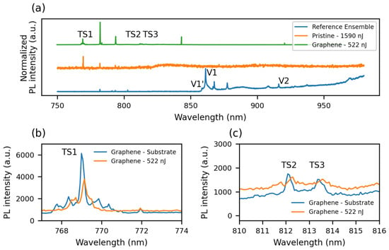
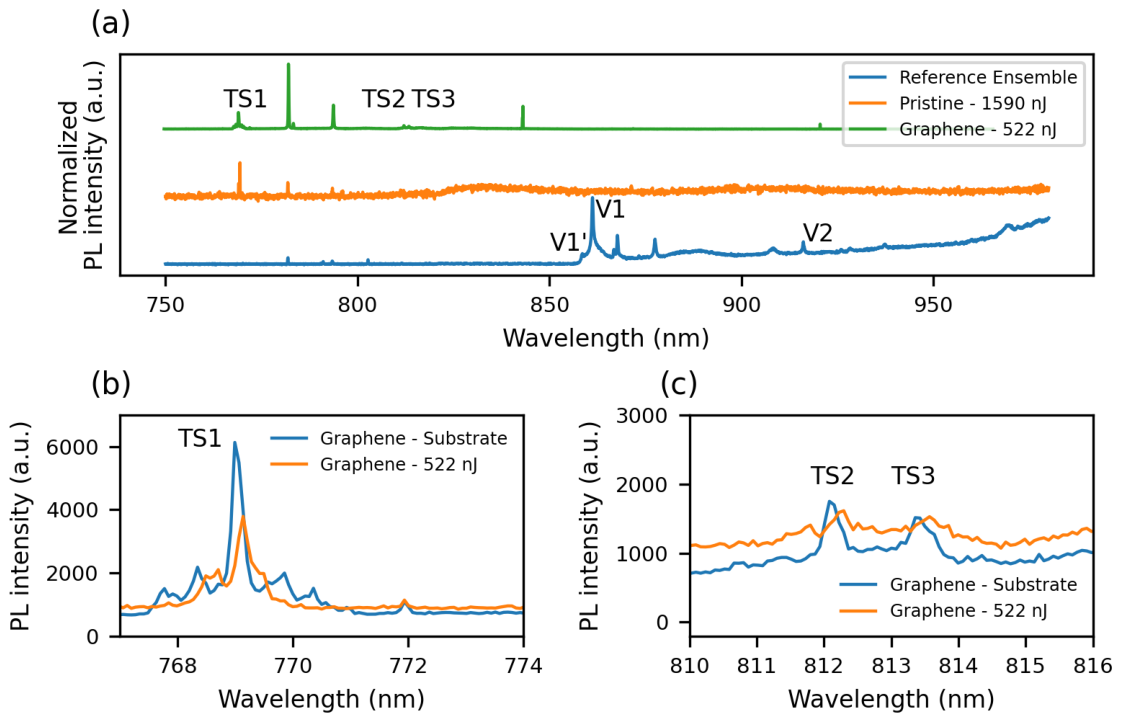
Figure 6a compares the cryogenic spectra of three 4H-SiC samples: ion-implanted reference sample, laser-written pristine sample, and laser-written sample with a graphene layer. The reference sample exhibits peaks associated with silicon vacancies (), including V1′ at 858 nm, V1 at 861 nm, and V2 at 916 nm, in agreement with the literature.
Figure 6.
(a) PL spectra at 4.3 K taken on a reference ion implanted sample which is compared to a laser-written spot at 1590 nJ on the pristine sample and a laser-written spot at 522 nJ on the sample with graphene. Peaks associated with are labeled V1′ (858 nm), V1 (861 nm) and V2 (916 nm). Peaks associated with the TS center are labeled TS1 (769 nm), TS2 (812 m) and TS3 (813 nm). (b,c) Low temperature spectra (4.3 K) of the sample with graphene taken on an unprocessed area (blue) and a laser-written spot (522 nJ) (orange). (b) presents a zoomed-in view around TS1, whereas (c) shows the regions around TS2 and TS3.
We do not observe ZPL emission from at cryogenic temperatures in both laser-written samples. In contrast, our room-temperature spectra and lifetime measurements strongly suggested the localized formation of (see Figure 3c and Figure 5d). As no other common intrinsic defect in 4H-SiC is known to produce a broad PL emission band in this spectral range [44], this suggests that emission may not originate from well defined centers, but rather -related centers in a highly strained laser-damaged environment. These findings align with those reported in [44], where centers were detected in laser-written regions but only with a weak enhancement relative to the non-irradiated substrate. Furthermore, the Raman measurements discussed above show that even at the lowest pulse energy of 60 nJ used in this work, the intensities of the main 4H-SiC Raman peaks (TO(), TO() and LO()) are reduced relative to those measured in unprocessed regions of the substrates, indicating degradation of the crystal quality. Moreover, as summarized in Table 1, previous laser writing work performed at the same 1030 nm wavelength did not show ZPL related to , only PL creation and typical room temperature spectra were observed. centers occurring before laser writing in our substrates were likely eliminated due to the high-temperature annealing for the pristine sample and the graphene growth for the other sample.
The PL spectrum of the sample with graphene exhibits peaks corresponding to the TS center at 769 nm, 812 nm, and 813 nm (TS1, TS2, and TS3, respectively) [49]. To determine whether TS centers form during laser writing or graphene growth, we analyzed spectra from a laser-written spot (522 nJ) and an unprocessed region of the substrate, as shown in zoom-in views in Figure 6b,c. On Figure 6b TS1 appears to be 41% weaker on the laser-written spots at 522 nJ than on an unprocessed region of the substrate, while TS2 and TS3 are broadened indicating that TS centers originate from the graphene growth process and not from laser irradiation.
The TS defect is known to withstand high annealing temperatures, but its microscopic origin remains uncertain and TS centers cannot serve as indicators for studying the laser-writing process. The absence of in laser-written regions may suggest that high temperatures in the processed volume lead to their removal via annealing. Moreover, for centers to exhibit PL, they must be in their negatively charged state. Charge-state alterations caused by the presence of other defects may therefore suppress PL emission.
Moreover, we investigated the near-infrared (NIR) PL using a dedicated setup optimized for detection above 1000 nm. Within this wavelength range falls the PL of divancancy defect in SiC. The samples were cooled down to 5 K in a cryostat (attoDRY800, attocube systems GmbH, Haar, Germany), and different excitation wavelengths were employed: 730 nm and 915 nm from a Ti:Sa Matisse CR laser (Sirah Lasertechnik GmbH, Grevenbroich, Germany), and 810 nm laser diode (EYP-RWL-0808-00800-4000 BFW09-0000, Toptica, Graefelfing, Germany). The excitation beams were focused onto the samples and PL was collected using a 100×, NA 0.9 objective (Carl Zeiss Microscopy GmbH, Oberkochen, Germany). Reflected laser light was removed from the collected PL using dichroic mirrors and a set of long-pass filters before being sent to a spectrometer (SpectraPro HRS 750 equipped with a NIRvana HS camera, Teledyne Princeton Instruments, Trenton, NJ, USA).
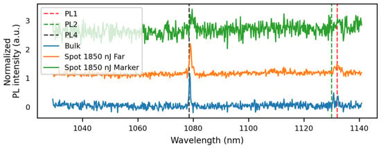
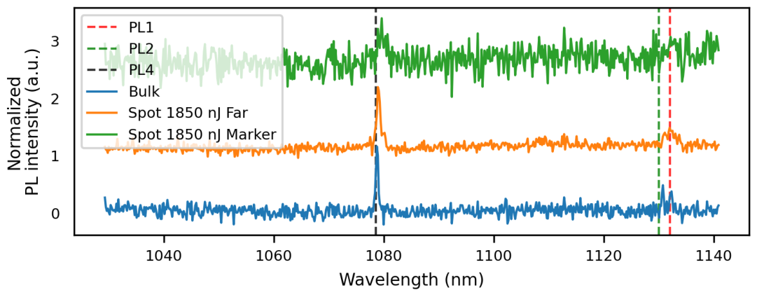
The sample with a graphene layer was investigated under 810 nm excitation; however, no PL peaks associated with the divacancy were observed. In contrast, the pristine sample was studied under 915 nm excitation with a 1000 nm long-pass filter. Multiple spectra were recorded both from unprocessed bulk regions (reference) and from laser-written spots at 1850 nJ, taken close to and far from markers; example spectra are shown in Figure 7.
Figure 7.
PL spectra at 5K taken on the pristine 4H-SiC sample at different position, unprocessed region (blue), around a written spot at 1850 nJ far from the markers (orange) around a written spot at 1850 nJ close to the markers (green).
In the reference spectra from an unprocessed region, PL peaks characteristic of the divacancy are visible [50,51]: PL1 (1132 nm), PL2 (1130 nm), and PL4 (1078 nm). These centers were either present natively in the crystal or formed during the annealing step at 800 °C. At the laser-written spots, the same spectral features can be identified; however, they appear broadened compared to the reference. This broadening is attributed to lattice damage induced by the laser writing process, and is most pronounced around the alignment markers, where the crystal damage is most severe. The absence of any PL intensity enhancement and the spectral broadening of the divacancy-related peaks, suggests that the laser writing process did not generate additional divacancies, but instead degraded or partially destroyed the ones already present before laser processing.
4. Discussion
We investigated the effect of epitaxial graphene on HPSI SiC on the creation of luminescent defects under femtosecond laser irradiation. We employ a commercial HPSI substrate and an industrial grade laser system to test broader applicability of the laser writing method. We observed a much lower intensity threshold to create PL defects on the sample with graphene compared to the pristine sample, suggesting graphene alters the local absorption and energy deposition conditions on the 4H-SiC surface during laser writing. While this might not necessarily be useful when creating color centers due to the high non-linearity of this process, the application of graphene might improve local surface annealing techniques using laser pulses. In accordance with previous work, we do not observe efficient creation of or divacancies centers, while spots with intense PL seem to be connected with strong surface structures (dimples) in a reference sample without graphene. Despite strong surface modification, we do not see the signature of amorphous materials. To optimize the process, 4H-SiC substrate with a 4H-SiC epitaxial layer with a more favorable doping could be investigated as well as shorter laser wavelength and stronger focusing to enhance non-linear effects in comparison to sample heating. Our work supports the finding, that creation using femtosecond laser pulses requires sophisticated optimization of laser parameters as well as employed SiC material.
Author Contributions
Methodology, Y.A., A.F., P.F., S.W., and M.S.; investigation, Y.A., A.F., P.F., S.W., M.S., J.H., and D.H.; resources, Y.A., A.F., P.F., S.W., M.S., and D.H.; writing—original draft preparation, Y.A.; writing—review and editing, all authors; visualization, Y.A.; supervision, E.N., C.B., J.L., and F.K.; project administration, E.N., C.B., J.L., and F.K.; funding acquisition, E.N., C.B., J.L., and F.K. All authors have read and agreed to the published version of the manuscript.
Funding
This work was funded by the Deutsche Forschungsgemeinschaft (DFG, German Research Foundation)—Project No. 429529648–TRR 306 QuCoLiMa (“Quantum Cooperativity of Light and Matter”). EN acknowledges support from the Quantum-Initiative Rhineland-Palatinate (QUIP). FK acknowledges support by the Luxembourg National Research Fund (FNR) via the PEARL chair “AQuaTSiC” under grant agreement 17792569, as well as the European Research Council for the project “Q-Chip” under grant agreement 101171067. FK and JH acknowledge further the European Union’s Horizon 2020 Research and Innovation Programme via the QuantERA project “SiCqurTech” under grant agreement 101017733, as well as the Horizon Europe Programme for the Flagship project “QIA” under grant agreement 101102140.
Data Availability Statement
All data supporting the results presented in this study are available in the Zenodo repository under DOI: https://doi.org/10.5281/zenodo.20526197 (accessed on 15 July 2026).
Acknowledgments
We thank Stefan Dix (RPTU, work-group A. Widera) and Thomas Utz (RPTU, work-group G. von Freymann) for additional experiments on laser writing and Konstantin Gröpl (RPTU, work-group V. Schünemann) for his help with the Raman measurements. We thank Johannes Lehmeyer and Michael Krieger (FAU Erlangen, work-group H. Weber) for additional PL measurements of laser irradiated samples as well as the growth of the epitaxial graphene layer. We acknowledge Christoph Döring for performing EDX measurements on the laser irradiated samples.
Conflicts of Interest
The authors declare no conflicts of interest.
References
- Lukin, D.M.; Guidry, M.A.; Vučković, J. Integrated Quantum Photonics with Silicon Carbide: Challenges and Prospects. PRX Quantum 2020, 1, 020102. [Google Scholar] [CrossRef] [Scilit]
- Castelletto, S.; Boretti, A. Chip-scale quantum sensors based on an integrated silicon carbide photonic platform. J. Phys. Photonics 2025, 7, 041001. [Google Scholar] [CrossRef] [Scilit]
- Sörman, E.; Son, N.T.; Chen, W.M.; Kordina, O.; Hallin, C.; Janzén, E. Silicon vacancy related defect in 4H and 6H SiC. Phys. Rev. B 2000, 61, 2613–2620. [Google Scholar] [CrossRef] [Scilit]
- Singh, H.; Anisimov, A.N.; Breev, I.D.; Baranov, P.G.; Suter, D. Optical spin initialization of spin-3/2 silicon vacancy centers in 6H-SiC at room temperature. Phys. Rev. B 2021, 103, 104103. [Google Scholar] [CrossRef] [Scilit]
- Falk, A.L.; Klimov, P.V.; Buckley, B.B.; Ivády, V.; Abrikosov, I.A.; Calusine, G.; Koehl, W.F.; Gali, Á.; Awschalom, D.D. Electrically and Mechanically Tunable Electron Spins in Silicon Carbide Color Centers. Phys. Rev. Lett. 2014, 112, 187601. [Google Scholar] [CrossRef] [Scilit] [PubMed]
- Nagy, R.; Niethammer, M.; Widmann, M.; Chen, Y.C.; Udvarhelyi, P.; Bonato, C.; Hassan, J.U.; Karhu, R.; Ivanov, I.G.; Son, N.T.; et al. High-fidelity spin and optical control of single silicon-vacancy centres in silicon carbide. Nat. Commun. 2019, 10, 1954. [Google Scholar] [CrossRef] [Scilit] [PubMed]
- Carter, S.G.; Soykal, O.O.; Dev, P.; Economou, S.E.; Glaser, E.R. Spin coherence and echo modulation of the silicon vacancy in 4H-SiC at room temperature. Phys. Rev. B 2015, 92, 161202(R). [Google Scholar] [CrossRef] [Scilit]
- Janzén, E.; Gali, A.; Carlsson, P.; Gällström, A.; Magnusson, B.; Son, N.T. The silicon vacancy in SiC. Phys. B 2009, 404, 4354–4358. [Google Scholar] [CrossRef] [Scilit]
- Lukin, D.M.; Guidry, M.A.; Yang, J.; Ghezellou, M.; Mishra, S.D.; Abe, H.; Ohshima, T.; Ul-Hassan, J.; Vučković, J. Optical superradiance of a pair of color centers in an integrated silicon-carbide-on-insulator microresonator. arXiv 2022, arXiv:2202.04845. [Google Scholar] [CrossRef] [Scilit]
- Lukin, D.M.; Guidry, M.A.; Yang, J.; Ghezellou, M.; Deb Mishra, S.; Abe, H.; Ohshima, T.; Ul-Hassan, J.; Vučković, J. Two-Emitter Multimode Cavity Quantum Electrodynamics in Thin-Film Silicon Carbide Photonics. Phys. Rev. X 2023, 13, 011005. [Google Scholar] [CrossRef] [Scilit]
- Wang, J.F.; Liu, L.; Liu, X.D.; Li, Q.; Cui, J.M.; Zhou, D.F.; Zhou, J.Y.; Wei, Y.; Xu, H.A.; Xu, W.; et al. Magnetic detection under high pressures using designed silicon vacancy centres in silicon carbide. Nat. Mater. 2023, 22, 489–494. [Google Scholar] [CrossRef] [Scilit] [PubMed]
- Berger, C.; Song, Z.; Li, T.; Li, X.; Ogbazghi, A.Y.; Feng, R.; Dai, Z.; Marchenkov, A.N.; Conrad, E.H.; First, P.N.; et al. Ultrathin Epitaxial Graphite:2D Electron Gas Properties and a Route toward Graphene-based Nanoelectronics. J. Phys. Chem. B 2004, 108, 19912–19916. [Google Scholar] [CrossRef] [Scilit]
- Ohta, T.; El Gabaly, F.; Bostwick, A.; McChesney, J.L.; Emtsev, K.V.; Schmid, A.K.; Seyller, T.; Horn, K.; Rotenberg, E. Morphology of graphene thin film growth on SiC(0001). New J. Phys. 2008, 10, 023034. [Google Scholar] [CrossRef] [Scilit]
- Emtsev, K.V.; Bostwick, A.; Horn, K.; Jobst, J.; Kellogg, G.L.; Ley, L.; McChesney, J.L.; Ohta, T.; Reshanov, S.A.; Röhrl, J.; et al. Towards wafer-size graphene layers by atmospheric pressure graphitization of silicon carbide. Nat. Mater. 2009, 8, 203–207. [Google Scholar] [CrossRef] [Scilit] [PubMed]
- Rühl, M.; Bergmann, L.; Krieger, M.; Weber, H.B. Stark tuning of the Silicon Vacancy in Silicon Carbide. Nano Lett. 2020, 20, 658. [Google Scholar] [CrossRef] [Scilit] [PubMed]
- Yazdi, G.R.; Vasiliauskas, R.; Iakimov, T.; Zakharov, A.; Syväjärvi, M.; Yakimova, R. Growth of large area monolayer graphene on 3C-SiC and a comparison with other SiC polytypes. Carbon 2013, 57, 477–484. [Google Scholar] [CrossRef] [Scilit]
- Zebardastan, N.; Bradford, J.; Lipton-Duffin, J.; MacLeod, J.; Ostrikov, K.; Tomellini, M.; Motta, N. High quality epitaxial graphene on 4H-SiC by face-to-face growth in ultra-high vacuum. Nanotechnology 2023, 34, 105601. [Google Scholar] [CrossRef] [Scilit] [PubMed]
- Novoselov, K.S.; Jiang, Z.; Zhang, Y.; Morozov, S.V.; Stormer, H.L.; Zeitler, U.; Maan, J.C.; Boebinger, G.S.; Kim, P.; Geim, A.K. Room-Temperature Quantum Hall Effect in Graphene. Science 2007, 315, 1379. [Google Scholar] [CrossRef] [Scilit] [PubMed]
- Novoselov, K.S.; Fal’ko, V.I.; Colombo, L.; Gellert, P.R.; Schwab, M.G.; Kim, K. A roadmap for graphene. Nature 2012, 490, 192–200. [Google Scholar] [CrossRef] [Scilit] [PubMed]
- Lin, Y.M.; Dimitrakopoulos, C.; Jenkins, K.A.; Farmer, D.B.; Chiu, H.Y.; Grill, A.; Avouris, P. 100-GHz Transistors from Wafer-Scale Epitaxial Graphene. Science 2010, 327, 662. [Google Scholar] [CrossRef] [Scilit] [PubMed]
- Tamura, K.; Tang, C.; Ogiura, D.; Suwa, K.; Fukidome, H.; Takida, Y.; Minamide, H.; Suemitsu, T.; Otsuji, T.; Satou, A. Fast and sensitive terahertz detection with a current-driven epitaxial-graphene asymmetric dual-grating-gate field-effect transistor structure. APL Photonics 2022, 7, 126101. [Google Scholar] [CrossRef] [Scilit]
- Rufangura, P.; Folland, T.G.; Agrawal, A.; Caldwell, J.D.; Iacopi, F. Towards low- loss on-chip nanophotonics with coupled graphene and silicon carbide: A review. J. Phys. Mater. 2020, 3, 032005. [Google Scholar] [CrossRef] [Scilit]
- Wang, J.; Zhang, X.; Zhou, Y.; Li, K.; Wang, Z.; Peddibhotla, P.; Liu, F.; Bauerdick, S.; Rudzinski, A.; Liu, Z.; et al. Scalable Fabrication of Single Silicon Vacancy Defect Arrays in Silicon Carbide Using Focused Ion Beam. ACS Photonics 2017, 4, 1054–1059. [Google Scholar] [CrossRef] [Scilit]
- Wang, J.F.; Li, Q.; Yan, F.F.; Liu, H.; Guo, G.P.; Zhang, W.P.; Zhou, X.; Guo, L.P.; Lin, Z.H.; Cui, J.M.; et al. On-Demand Generation of Single Silicon Vacancy Defects in Silicon Carbide. ACS Photonics 2019, 6, 1736–1743. [Google Scholar] [CrossRef] [Scilit]
- Chen, Y.C.; Salter, P.S.; Niethammer, M.; Widmann, M.; Kaiser, F.; Nagy, R.; Morioka, N.; Babin, C.; Erlekampf, J.; Berwian, P.; et al. Laser writing of scalable single color centers in silicon carbide. Nano Lett. 2019, 19, 2377–2383. [Google Scholar] [CrossRef] [Scilit] [PubMed]
- Castelletto, S.; Almutairi, A.F.M.; Kumagai, K.; Katkus, T.; Hayasaki, Y.; Johnson, B.C.; Juodkazis, S. Photoluminescence in hexagonal silicon carbide by direct femtosecond laser writing. Opt. Lett. 2018, 43, 6077. [Google Scholar] [CrossRef] [Scilit] [PubMed]
- Zhou, Z.; Xu, Z.; Song, Y.; Shi, C.; Zhang, K.; Dong, B. Silicon Vacancy Color Centers in 6H-SiC Fabricated by Femtosecond Laser Direct Writing. Nanomanuf. Metrol. 2023, 6, 7. [Google Scholar] [CrossRef] [Scilit]
- Liu, X.; Luo, J.; Ye, J.; Fu, J.; Yang, Q.; Wang, Y.; Chen, X.; Tao, T.; Liu, B.; Xu, Q.; et al. Color centers and crystal structural transformations induced by femtosecond laser writing in 4H-SiC. J. Appl. Phys. 2025, 137, 123101. [Google Scholar] [CrossRef] [Scilit]
- Hao, Z.-H.; He, Z.-X.; Maksimovic, J.; Katkus, T.; Xu, J.-S.; Juodkazis, S.; Li, C.-F.; Castelletto, S. Laser Writing and Spin Control of Near-Infrared Emitters in Silicon Carbide. ACS Photonics 2025, 12, 1552–1560. [Google Scholar] [CrossRef] [Scilit]
- Pezzagna, S.; Wildanger, D.; Mazarov, P.; Wieck, A.D.; Sarov, Y.; Rangelow, I.; Naydenov, B.; Jelezko, F.; Hell, S.W.; Meijer, J. Nanoscale Engineering and Optical Addressing of Single Spins in Diamond. Small 2010, 6, 2117–2121. [Google Scholar] [CrossRef] [Scilit] [PubMed]
- Dong, B.; Sun, Q.; Xu, Z. Enhancing VSi fluorescence collection efficiency via 3D direct-written SiC immersion lenses with hollow cylindrical vector beam. Opt. Laser Technol. 2026, 197, 114766. [Google Scholar] [CrossRef] [Scilit]
- Gutsche, J.; Zand, A.; Bültel, M.; Widera, A. Revealing superradiant emission in the single-to-bulk transition of quantum emitters in nanodiamond agglomerates. New J. Phys. 2022, 24, 053039. [Google Scholar] [CrossRef] [Scilit]
- Wang, C.; Kurokawa, S.; Doi, T.; Yuan, J.; Fan, L.; Mitsuhara, M.; Lu, H.; Yao, W.; Zhang, Y.; Zhang, K. SEM, AFM and TEM Studies for Repeated Irradiation Effect of Femtosecond Laser on 4H-SiC Surface Morphology at Near Threshold Fluence. ECS J. Solid State Sci. Technol. 2018, 7, P29–P34. [Google Scholar] [CrossRef] [Scilit]
- Widmann, M.; Lee, S.Y.; Rendler, T.; Son, N.T.; Fedder, H.; Paik, S.; Yang, L.P.; Zhao, N.; Yang, S.; Booker, I.; et al. Coherent control of single spins in silicon carbide at room temperature. Nat. Mater. 2015, 14, 164–168. [Google Scholar] [PubMed]
- Bockstedte, M.; Mattausch, A.; Pankratov, O. Ab Initio Study Annealing Vacanc. Interstitials Cubic SiC: Vacancy-Interstitial Recomb. Aggreg. Carbon Interstitials. Phys. Rev. B 2004, 69, 235202. [Google Scholar] [CrossRef] [Scilit]
- Wang, X.; Zhao, M.; Bu, H.; Zhang, H.; He, X.; Wang, A. Formation and annealing behaviors of qubit centers in 4H-SiC from first principles. J. Appl. Phys. 2013, 114, 194305. [Google Scholar] [CrossRef] [Scilit]
- Dong, T.; Sparkes, M.; Durkan, C.; O’Neill, W. Evaluating femtosecond laser ablation of graphene on SiO2/Si substrate. J. Laser Appl. 2016, 28, 022202. [Google Scholar] [CrossRef] [Scilit]
- Roberts, A.; Cormode, D.; Reynolds, C.; Newhouse-Illige, T.; LeRoy, B.J.; Sandhu, A.S. Response of graphene to femtosecond high-intensity laser irradiation. Appl. Phys. Lett. 2011, 99, 051912. [Google Scholar] [CrossRef] [Scilit]
- Chen, J.; Xie, X.; Peng, Q.; He, Z.; Hu, W.; Ren, Q.; Long, J. Effect of surface roughness on femtosecond laser ablation of 4H-SiC substrates. J. Cent. South Univ. 2022, 29, 3294–3303. [Google Scholar] [CrossRef] [Scilit]
- Wang, L.; Zhao, Y.; Yang, Y.; Zhang, M.; Zhao, Y. Experimental Investigation on Ablation of 4H-SiC by Infrared Femtosecond Laser. Micromachines 2022, 13, 1291. [Google Scholar] [CrossRef] [Scilit] [PubMed]
- Wang, J.; Song, Y.; Dong, B.; Zhao, Y.; Sun, Q.; Yan, M.; Yao, C.; Du, Q.; Xu, Z. Femtosecond laser controllable annealing for color centers based on ion-implanted silicon carbide substrate. Ceram. Int. 2024, 50, 46566–46578. [Google Scholar] [CrossRef] [Scilit]
- Nair, R.R.; Blake, P.; Grigorenko, A.N.; Novoselov, K.S.; Booth, T.J.; Stauber, T.; Peres, N.M.R.; Geim, A.K. Fine Structure Constant Defines Visual Transparency of Graphene. Science 2008, 320, 1308. [Google Scholar] [CrossRef] [Scilit] [PubMed]
- Yan, M.; Zhao, J.; Song, Y.; Dong, B.; Duan, Y.; Wang, J.; Sun, Q.; Xu, Z. Crater-shaped Enrichment of VSi Color Centers in 4H-SiC using Single-Pulse Near-Infrared Femtosecond Laser Processing. arXiv 2024, arXiv:2407.19470. [Google Scholar]
- Castelletto, S.; Maksimovic, J.; Katkus, T.; Ohshima, T.; Johnson, B.C.; Juodkazis, S. Color Centers Enabled by Direct Femto-Second Laser Writing in Wide Bandgap Semiconductors. Nanomaterials 2020, 11, 72. [Google Scholar] [CrossRef] [Scilit] [PubMed]
- Liu, J.; Xu, Z.; Song, Y.; Wang, H.; Dong, B.; Li, S.; Ren, J.; Li, Q.; Rommel, M.; Gu, X.; et al. Confocal photoluminescence characterization of silicon-vacancy color centers in 4H-SiC fabricated by a femtosecond laser. Nanotechnol. Precis. Eng. 2020, 3, 218–228. [Google Scholar] [CrossRef] [Scilit]
- Steeds, J.; Evans, G.; Danks, L.; Furkert, S.; Voegeli, W.; Ismail, M.; Carosella, F. Transmission electron microscope radiation damage of 4H and 6H SiC studied by photoluminescence spectroscopy. Diam. Relat. Mater. 2002, 11, 1923–1945. [Google Scholar] [CrossRef] [Scilit]
- Kraus, H.; Simin, D.; Kasper, C.; Suda, Y.; Kawabata, S.; Kada, W.; Honda, T.; Hijikata, Y.; Ohshima, T.; Dyakonov, V.; et al. Three-dimensional proton beam writing of optically active coherent vacancy spins in silicon carbide. Nano Lett. 2017, 17, 2865–2870. [Google Scholar] [CrossRef] [Scilit] [PubMed]
- Hain, T.C.; Fuchs, F.; Soltamov, V.A.; Baranov, P.G.; Astakhov, G.V.; Hertel, T.; Dyakonov, V. Excitation and recombination dynamics of vacancy-related spin centers in silicon carbide. J. Appl. Phys. 2014, 115. [Google Scholar] [CrossRef] [Scilit]
- Rühl, M.; Ott, C.; Götzinger, S.; Krieger, M.; Weber, H. Controlled generation of intrinsic near-infrared color centers in 4H-SiC via proton irradiation and annealing. Appl. Phys. Lett. 2018, 113, 122102. [Google Scholar] [CrossRef] [Scilit]
- Koehl, W.F.; Buckley, B.B.; Heremans, F.J.; Calusine, G.; Awschalom, D.D. Room temperature coherent control of defect spin qubits in silicon carbide. Nature 2011, 479, 84–87. [Google Scholar] [CrossRef] [Scilit] [PubMed]
- Magnusson, B.; Son, N.T.; Csóré, A.; Gällström, A.; Ohshima, T.; Gali, A.; Ivanov, I.G. Excitation properties of the divacancy in 4H-SiC. Phys. Rev. B 2018, 98, 195202. [Google Scholar] [CrossRef] [Scilit]

Disclaimer/Publisher’s Note: The statements, opinions and data contained in all publications are solely those of the individual author(s) and contributor(s) and not of MDPI and/or the editor(s). MDPI and/or the editor(s) disclaim responsibility for any injury to people or property resulting from any ideas, methods, instructions or products referred to in the content. |
© 2026 by the authors. Licensee MDPI, Basel, Switzerland. This article is an open access article distributed under the terms and conditions of the Creative Commons Attribution (CC BY) license.