


Abstract
CsPbI2Br, an all-inorganic cesium–lead mixed-halide perovskite, has established itself as a leading contender for next-generation photovoltaics, owing to its near-optimal direct bandgap, exceptional thermal stability, and favorable optoelectronic characteristics. These attributes make it a versatile candidate for both high-efficiency single-junction devices and wide-bandgap top cells in tandem architectures with silicon or low-bandgap perovskites. However, the commercialization of CsPbI2Br perovskite solar cells (PSCs) is severely hindered by inherent interfacial challenges, including halide segregation under operational stress, high density of interfacial defects, energy-level misalignment between the perovskite and charge transport layers (CTLs), and chemical incompatibility at hetero-interfaces. These factors limit power conversion efficiency (PCE) and long-term operational stability. Interface engineering has thus become the pivotal strategy to address these bottlenecks, enabling transformative improvements in device performance. This review comprehensively summarizes the state-of-the-art interface engineering strategies for CsPbI2Br PSCs, including molecular passivation, construction of 2D/3D heterostructures, design of composite interlayers, and development of dopant-free, stable CTLs. The underlying mechanisms of defect passivation, non-radiative recombination suppression, energy-level alignment optimization, and ion migration inhibition are systematically elucidated. Furthermore, we discuss critical remaining challenges, including the trade-off between phase stability and optoelectronic quality, interfacial delamination due to thermal expansion mismatch, and scalable fabrication of interface-modified large-area devices. Finally, future research directions are proposed, emphasizing the development of multifunctional interfacial materials, all-inorganic interface architectures, in situ characterization combined with computational modeling, and integration into tandem photovoltaic systems. By consolidating current knowledge and highlighting promising frontiers, this review aims to guide the rational design of high-performance, stable, and commercially viable CsPbI2Br PSCs, accelerating their role in the global transition toward renewable energy.
1. Introduction
The global transition towards a carbon-neutral future has galvanized unprecedented innovation in renewable energy technologies, with photovoltaics (PV) standing as a pivotal pillar for sustainable power generation [1]. Among emerging PV materials, metal-halide PSCs have instigated a paradigm shift over the past decade. Due to their exceptional optoelectronic properties, such as high absorption coefficients, long charge-carrier diffusion lengths, and tunable bandgaps, and coupled with their facile and low-cost solution processability, PSCs have achieved certified PCEs exceeding 26% for single-junction devices, competing with the established silicon technology [2,3,4]. However, the commercial viability of dominant organic–inorganic hybrid perovskites (e.g., MAPbI3, FAPbI3) is critically hampered by their intrinsic instability under thermal stress, moisture, and continuous illumination, largely due to the volatile nature of organic A-site cations (MA+, FA+) [5,6].
In response, all-inorganic cesium–lead halide perovskites (CsPbX3, X = I, Br, Cl) have emerged as highly attractive alternatives, offering superior thermal and phase stability while preserving excellent optoelectronic performance [7]. Within this family, cesium–lead mixed halide CsPbI2Br has garnered significant attention as a frontrunner for practical applications. CsPbI2Br uniquely amalgamates a near-ideal direct bandgap of ~1.9 eV, which is well-matched to the AM 1.5G solar spectrum, with remarkable thermal stability, maintaining its photoactive cubic (α) phase at temperatures exceeding 300 °C, far surpassing the degradation thresholds of hybrid analogues [8,9]. This combination makes it an optimal candidate not only for efficient single-junction cells but also as a high-performance wide-bandgap top cell in tandem architectures with silicon or low-bandgap perovskite bottom cells [10,11,12].
Despite these intrinsic merits, the performance of CsPbI2Br PSCs is fundamentally constrained by a series of interfacial challenges that limit both efficiency and long-term operational stability, which constitutes the primary bottleneck for their commercialization [13,14]. First, halide segregation under operational biases (light, heat, electric field) leads to the formation of iodine-rich and bromine-rich domains, causing local bandgap fluctuations and exacerbating non-radiative recombination losses. This phenomenon is particularly detrimental to the stability of tandem cells [15]. Second, a high density of interfacial defects, including iodine vacancies (VI), bromine vacancies (VBr), and undercoordinated Pb2+ ions, serves as Shockley–Read–Hall (SRH) recombination centers, which severely restricts the achievable open-circuit voltage (Voc) [16]. Advanced simulations highlight the complex role of specific defects, with VI significantly reducing carrier lifetimes [17]. Third, energy-level misalignment between CsPbI2Br and adjacent CTLs creates significant barriers for charge extraction, which results in carrier accumulation, an increase in series resistance, and losses in the fill factor (FF) [18]. Fourth, chemical incompatibility and redox reactions at interfaces, such as those between metal oxide hole transport layers (HTLs) like nickel oxide (NiOx) and halide ions, can lead to accelerated degradation and phase instability [19]. These interfacial issues have limited the champion PCEs of single-junction CsPbI2Br PSCs to the range of 16–18%, which is still below their theoretical potential [20,21].
Interface engineering has consequently risen as the cornerstone strategy to address these multifaceted challenges. This is because the performance, stability, and scalability of PSCs are primarily determined by the physicochemical properties of crucial hetero-interfaces, such as ETL/CsPbI2Br, CsPbI2Br/HTL, and electrode/CTL junctions [22]. Rational design and modification of these interfaces have enabled transformative breakthroughs, such as molecular passivation via tailored self-assembled monolayers (SAMs), ionic liquids (ILs), or functional small molecules, as well as the construction of 2D/3D heterostructures or composite interlayers. Moreover, the development of dopant-free, stable CTLs has been deployed to simultaneously passivate defects, optimize energy-level alignment, suppress ion migration, and enhance interfacial adhesion [23,24]. For example, acetate-assisted modification of titanium dioxide (TiO2) ETLs with Zn(Ac)2 has been shown to passivate oxygen vacancies and regulate the crystallization of CsPbI2Br, thereby boosting the PCE of carbon-based devices [25]. Similarly, molecular passivators coordinate with undercoordinated Pb2+, thereby enhancing film quality and device performance [26].
Nevertheless, significant hurdles still persist. The inherent trade-off between phase stability and optoelectronic quality in CsPbI2Br, its susceptibility to interfacial delamination due to thermal expansion mismatch, and the scalability of lab-based interface engineering to industrially viable, large-area fabrication processes remain critical challenges [27,28]. Future progress is contingent upon the development of multifunctional interfacial materials that can simultaneously address defect passivation, band alignment, chemical stabilization, and mechanical reinforcement, as guided by advanced in situ characterization and computational modeling [29,30].
This review provides a comprehensive and focused analysis of the latest advances in interface engineering for CsPbI2Br PSCs. We commence with an overview of fundamental device architectures (n-i-p and p-i-n) and the pivotal functional roles of interfaces in charge dynamics and degradation pathways. Subsequently, we present a systematic examination of state-of-the-art engineering strategies for each critical interface, elucidating the underlying mechanisms of defect passivation, recombination suppression, and stability enhancement. This is followed by a critical discussion on persistent challenges and future research directions, emphasizing multifunctional design, all-inorganic interfaces, scalable processing, and integration into tandem photovoltaic systems. By consolidating current knowledge and highlighting promising frontiers, this review aims to serve as a foundational resource to accelerate the development of efficient, stable, and commercially viable CsPbI2Br-based solar cells. Figure 1 summarizes of interface engineering strategies, key challenges, and future directions for CsPbI2Br PSCs.
Figure 1.
Summary of interface engineering strategies, key challenges, and future directions for CsPbI2Br PSCs.
2. The Device Architecture and Interface Functions of PSCs
2.1. Device Architecture
The evolution of PSCs is driven by device structural innovation, with interface engineering as the key enabler. Originating from DSSCs, the first breakthrough in 1979 modified a TiO2 electrode with a ruthenium complex for visible light sensitization [31], but suffered from low photocurrent due to limited dye chemisorption on the flat surface [32]. In 1991, O’Regan and Grätzel introduced a mesoporous TiO2 layer [33], which vastly increased the surface area, enhancing dye loading and the semiconductor interface. This architecture (mesoporous TiO2/dye/liquid I−/I3− electrolyte/counter electrode) achieved a PCE of 7.1–7.9%. However, the liquid electrolyte introduced critical interface issues, including high recombination at the TiO2/electrolyte interface, corrosiveness, and leakage, prompting the shift toward solid-state alternatives [34].
The initial PSSC used MAPbI3 (Figure 2A) as a sensitizer on TiO2 with a liquid electrolyte, achieving 3.8% PCE but suffering from corrosion and interface degradation [35]. Replacing the liquid electrolyte with a solid organic HTL (Spiro-OMeTAD) eliminated these issues, stabilized the perovskite/HTL interface, and raised PCE to 9.7% [36,37]. A major shift occurred when perovskites were redefined as active thin-film semiconductors rather than sensitizers. Snaith and colleagues replaced mesoporous TiO2 with a dielectric Al2O3 scaffold and deposited a MAPbI3−xClx layer as the light-absorbing component, achieving 10.9% PCE and establishing PSCs as a distinct technology [37]. Subsequent work showed that the mesoporous scaffold was unnecessary, leading to planar heterojunction structures with direct ETL/perovskite/HTL stacking, which reduced interfacial resistance from grain boundaries while preserving efficient charge separation (Figure 2A) [38]. Today, two main configurations dominate: conventional n-i-p and inverted p-i-n (Figure 2A). Both feature a perovskite absorber between ETL and HTL, but layer order dictates charge flow and interfacial properties.
Figure 2.
(A) Schematic illustration of perovskite solar cell development, device architectures (mesoporous, planar n–i–p, p–i–n). (B) Energy level alignment of transparent electrodes, ETLs, perovskite absorbers, and HTLs for evaluating band matching and charge transport properties. Reproduced or adapted from [16], with permission from Springer Nature, 2023.
In n-i-p (ETL/perovskite/HTL on TCO), light enters through the TCO and ETL. Photogenerated electrons move to the ETL and holes to the HTL, requiring precise energy-level alignment (Figure 2B). The ETL’s conduction band (CB) should be slightly below that of the perovskite for spontaneous electron injection, while the HTL’s valence band (VB) must align with the perovskite’s VB for hole extraction [39]. Mismatches cause carrier accumulation and recombination [40,41]. The mesoporous n-i-p variant, derived from DSSCs, uses a compact TiO2 layer plus a mesoporous TiO2 scaffold. TiO2 offers high mobility and stability, enabling a certified 14.1% PCE in 2013 [42]. However, high-temperature sintering (~500 °C) restricts flexible substrates like PET [43], and the large surface area introduces abundant defect sites (e.g., oxygen vacancies) that act as recombination centres. Surface passivation with self-assembled monolayers or oxide nanoclusters reduces trap states [44,45]. Insulating scaffolds such as ZrO2 or Al2O3, though not electron-transporting, improve Voc by reducing recombination at the perovskite/scaffold interface [37,46]. The planar n-i-p architecture eliminates the mesoporous layer, enabling low-temperature processing and simpler fabrication. Early planar devices suffered from poor perovskite coverage and voids [47], but optimized annealing raised efficiency to 11.4% [48], and thermal evaporation of perovskite yielded more homogeneous films with 15.4% [49]. Low-temperature SnO2 ETLs, processed via solution methods below 150 °C, achieved 17.2% [50], and surface passivation with phenethylammonium iodide (PEAI) boosted certified efficiency to 23.3% [24]. For HTLs, Spiro-OMeTAD remains the benchmark due to its good hole mobility and energy alignment, despite its high cost and moisture sensitivity [37]. Fluorinated isomeric analogues have pushed PCEs beyond 24.8% [39]. Inorganic NiOx offers improved stability and lower cost though its efficiency still trails optimized Spiro-OMeTAD devices in many configurations [51,52,53]. State-of-the-art n-i-p PSCs now exceed 25% using FAPbI3-based perovskites with a bandgap of 1.48 eV [54]. Persistent challenges include high-temperature fabrication requirements for mesoporous architectures, pinhole-induced shunting hazards in planar devices, and poor operational stability of HTL. Future efforts focus on flexible substrates, earth-abundant HTLs, and multifunctional interface engineering.
The inverted p-i-n structure (HTL/perovskite/ETL on TCO, Figure 2A) has gained prominence [55]. The HTL must efficiently extract holes and stabilize the HTL/perovskite interface. Organic PEDOT:PSS is widely used for its solution processability, high transparency, and low-temperature compatibility, but its intrinsic acidity (from PSS) and hygroscopicity degrade interfaces. Blending with polyTPD suppresses acid-induced reactions [56]. Inorganic NiOx offers superior chemical stability and a tunable work function (5.2–5.6 eV) [57]. Guo et al. pioneered NiOx in p-i-n devices [58], and Seok et al. achieved 17.3% via laser pulse deposition to improve film quality [59]. However, pristine NiOx has low intrinsic conductivity and high defect density (e.g., oxygen vacancies), and it can react with perovskite precursors, degrading the NiOx/perovskite interface [19,60]. Doping strategies, such as with the molecular dopant F6TCNNQ, have enhanced conductivity and optimised band alignment, yielding PCEs up to 22.1% [61]. For ETLs, the fullerene derivative PCBM is common due to high electron mobility, favourable CB alignment, and solution processability [62], but it can facilitate ion migration under prolonged illumination, disrupting energy levels. Inorganic oxides ZnO and SnO2 offer better chemical stability [63]. Replacing PCBM with ZnO improved interfacial stability, and a fully inorganic ETL stack achieved 18.5% [64]. Proper energy alignment (Figure 2B) and minimal chemical reactivity are essential for these ETL/perovskite interfaces.
Ultimately, device performance and stability are governed by four hetero-interfaces: electrode/ETL, ETL/perovskite, perovskite/HTL, and HTL/electrode. Each requires optimal energy-level alignment (Figure 2B) and defect passivation to suppress recombination and ensure efficient charge extraction, which remain central to ongoing research.
Electrode/ETL and HTL/Electrode Interfaces: These interfaces govern charge collection efficiency. For instance, in n-i-p devices, the work function of the transparent electrode (e.g., ITO, ~4.7 eV) must align well with the CB of the ETL (e.g., SnO2, ~4.2 eV) to minimize energy barriers for electron injection. Similarly, in p-i-n architectures, efficient hole extraction depends on matching the electrode work function (e.g., Ag, ~4.3 eV) with the VB of the HTL (e.g., PEDOT:PSS, ~5.2 eV). Mismatched energy levels at these contacts can lead to Ohmic losses and reduce the FF.
ETL/Perovskite and Perovskite/HTL Interfaces: These interfaces are critical for charge separation and extraction, directly influencing the Voc. An optimal offset (typically <0.3 eV) between the CB of the ETL and that of the perovskite, such as between SnO2 (~4.2 eV) and MAPbI3 (~3.9 eV), facilitates efficient electron injection while suppressing interfacial recombination. Conversely, excessive offsets promote carrier accumulation and increase recombination losses.
2.2. Working Mechanism
PSCs convert solar energy into electrical power through a series of photophysical and electrochemical steps, in which the interfaces between the CsPbI2Br absorber and CTLs critically influence charge-carrier behavior and device performance. The working mechanism can be broken down into four interrelated processes, each modulated by interfacial properties, as elaborated below.
Light Absorption: The process initiates with light absorption by the CsPbI2Br layer, which has a bandgap of ~1.91 eV, enabling efficient capture of visible light up to ~650 nm and covering a significant portion of the AM 1.5 G solar spectrum (Figure 3A) [65]. Absorption occurs as photons with energy above the bandgap excite electrons from the VB, which is primarily composed of Pb 6s and I/Br np orbitals, to the CB, predominantly formed by Pb 6p orbitals, thus creating holes in the VB [8,66]. A high absorption coefficient (>104 cm−1) near the band edge allows effective light harvesting even with thin films (~500–600 nm) [67]. This reduces the dependence on long carrier diffusion lengths and mitigates bulk recombination losses. However, the absorption efficiency is strongly dependent on the film quality. Specifically, poor crystallinity or the presence of pinholes facilitates light scattering, and grain boundaries act as defect nucleation sites that can propagate into CTLs [8].
Figure 3.
(A) Device structure and energy levels diagram of CsPbI2Br/organic TSCs, UV−vis spectra of CsPbI2Br, D18:Y6 and PM6:Y6 films. Reproduced or adapted from [65], with permission from Elsevier, 2022. (B) Bulk and interfacial non−radiative recombination currents at open−circuit as obtained on nip and pin−type cells with nearly flat quasi−Fermi levels and illustrates a solar cell as bucket with holes where the water level represents the cells’ VOC. Reproduced or adapted from [53], with permission from Royal Society of Chemistry, 2019.
Exciton Dissociation: Photoabsorption generates excitons (electron–hole pairs) in the absorber. Owing to its low exciton binding energy (<100 meV), CsPbI2Br enables spontaneous exciton dissociation into free charges in the bulk, without an external field [8,68]. Nonetheless, dissociation efficiency is highly sensitive to interfacial conditions. Poor electrical contact with the ETL or HTL distorts the local electric field, impeding separation. Furthermore, interfacial defects such as iodine vacancies (VI) or undercoordinated Pb2+ ions act as non-radiative recombination centers, quenching excitons and reducing free carrier density [16,69].
Charge Transport and Interface Dynamics: Once separated, free electrons and holes must transfer the CsPbI2Br/CTL interfaces efficiently to minimize recombination. This depends on two main factors: energy level alignment and interfacial defect density. For effective electron extraction, the ETL should have a conduction band minimum (CBM) slightly lower than that of CsPbI2Br (~−3.9 eV). Materials such as SnO2 (CBM ~−4.0 eV) and TiO2 (CBM ~−4.2 eV) provide favorable band offsets, promoting electron transfer [8]. Similarly, the HTL should have a valence band maximum (VBM) higher than that of CsPbI2Br (~−5.8 eV); NiOx (VBM ~−5.4 eV) and poly(triarylamine) (PTAA) (VBM ~−5.2 eV) facilitate hole extraction [16,57]. Misaligned energy levels cause significant losses. For instance, an overly low-lying CBM in TiO2 (>−4.3 eV) introduces an energy barrier, leading to electron accumulation and enhanced recombination (Figure 3B) [16,53]. An incompatible HTL can form a Schottky barrier, blocking hole extraction and reducing both Jsc and Voc (Figure 4A) [70]. Common intrinsic defects at CsPbI2Br interfaces, including VCs, VI, VBr, and antisite defects such as PbCs, originate from incomplete crystallization or chemical reactions with CTLs [71]. These introduce trap states that capture carriers, prolonging interface residence and increasing recombination probability [16,19,72].
Figure 4.
(A) Schematic representation of the band edge positions of the investigated HSCs based on values from UPS measurements, referenced to the vacuum level. Reproduced or adapted from [70], with permission from Royal Society of Chemistry, 2019. (B) Summary of absPL and TrPL measurements. Reproduced or adapted from [70], with permission from Royal Society of Chemistry, 2019. (C) Energy level diagram of the device and illustration of a dipole layer near the interface between the perovskite layer and CsAc/SnO2 hybrid layer. Reproduced or adapted from [73], with permission from American Chemical Society, 2025. (D) Schematic structure of the inverted PSC with a 2D/3D hybrid structure. Reproduced or adapted from [74], with permission from American Chemical Society, 2021. (E) Proposed mechanism illustrating 2−ThPy mediated perovskite crystal growth and defect passivation. Reproduced or adapted from [75], with permission from Wiley−VCH, 2020.
Charge Collection at Electrodes: After crossing the CTLs, carriers are collected at the electrodes. The front electrode (e.g., FTO or ITO) collects electrons from the ETL, and the back electrode (e.g., Au or carbon) collects holes from the HTL. The quality of these interfaces also affects device performance: poor adhesion between ITO and SnO2 increases series resistance (Rs) and reduces FF, whereas ohmic contact between PTAA and Au enables efficient hole collection. Carbon electrodes are attractive due to their stability and low cost, but their work function (~−5.0 eV) often mismatches with HTLs (e.g., PTAA at ~−5.2 eV). Interface modifications, such as SAMs, can mitigate this. For instance, a 2PACz SAM on carbon adjusts its work function to ~−5.2 eV, matching PTAA’s VBM and facilitating barrier-free hole extraction (Figure 4C) [70].
2.3. Interface Function of PSCs
Interfaces in PSCs serve as critical junctions that govern charge dynamics, materials compatibility, and long-term device stability. Interactions at the interfaces with ETLs, HTLs, and electrodes directly influence key performance parameters, such as Voc, Jsc, FF, and PCE, as well as device lifetime. This section elaborates on the core roles of major interfaces in PSCs, including ETL/perovskite, perovskite/HTL, and electrode/CTLs interfaces, integrating fundamental mechanisms with recent experimental insights.
Energy Level Alignment: Proper energy level alignment is essential for efficient charge separation and extraction in PSCs. Mismatched energy bands between the perovskite and CTLs introduce energy barriers that lead to charge accumulation, increased recombination, and significant Voc losses. Interface engineering aims to adjust the work function of transport materials or introduce dipole layers to align the CBM of the ETL and the VBM of the HTL with the CBM (~−3.9 eV) and VBM (~−5.8 eV) of CsPbI2Br, respectively. At the ETL/CsPbI2Br interface, metal oxides such as SnO2, TiO2, and ZnO are commonly used. However, their intrinsic work functions often misalign with those of CsPbI2Br. For instance, pristine SnO2 has a work function around −4.6 eV, resulting in a small but non-negligible electron extraction barrier [73]. Modification with SAMs or metal halides can tune SnO2’s work function closer to −4.0 eV, thereby minimizing the energy barrier and improving Jsc (Figure 4A). Similarly, at the CsPbI2Br/HTL interface, p-type materials like NiOx, PTAA, and P3HT often suffer from Fermi-level pinning caused by surface defects, which compromises built-in potential. For example, untreated NiOx has a work function near −5.3 eV, which is higher than the VBM of CsPbI2Br, creating a hole injection barrier. Introduction of interfacial modifiers, such as certain dyes, can passivate defects and adjust the work function of NiOx to approximately −5.6 eV, narrowing the energy barrier for hole extraction (Figure 4A) and significantly improving both Voc and PCE. The mixed-halide composition of CsPbI2Br (I−/Br−) also influences energy alignment [76]. Bromide tends to enrich at interfaces due to its lower migration energy, potentially widening the local bandgap by 0.05–0.1 eV. Halide-uniformity treatments can mitigate this effect (Figure 4B) and ensure consistent energy alignment across the interface.
Charge Dynamics Regulation: Charge dynamics at CsPbI2Br interfaces, including injection, transport, and recombination, directly affect Jsc and FF. The goal of interface modification is to suppress trap-assisted SRH recombination and enhance charge extraction, taking advantage of the high intrinsic carrier mobility of CsPbI2Br. Reducing interfacial resistance is key to facilitating charge transfer. For example, modifying SnO2 with fullerene derivatives can create efficient charge-transport channels, significantly reducing charge transfer resistance and accelerating electron extraction [77]. At the perovskite/HTL interface, conjugated polymers can coordinate with unsaturated Pb2+ sites on the perovskite surface while providing efficient pathways for hole transport, leading to higher hole mobility and improved Jsc and FF [78]. Non-radiative recombination at interfaces, often caused by deep-level traps such as Pb2+ vacancies and iodide interstitials, is a major source of Voc loss. Interface passivation strategies involving Lewis base molecules or halide salts can effectively neutralize these defects. For instance, treatment with PEAI forms a thin two-dimensional perovskite layer that passivates iodine vacancies and coordinates with undercoordinated Pb2+, markedly reducing interface trap density and non-radiative recombination (Figure 4D) [74].
Defect Passivation: CsPbI2Br perovskite films inherently contain defects such as unsaturated Pb2+ ions, halide vacancies, and grain boundary defects, which arise from rapid crystallization and lattice mismatch with adjacent layers. These intrinsic defects act as non-radiative recombination centers and facilitate ion migration, thereby detrimentally impacting device performance. Interface engineering emerges as an effective strategy to passivate such defects through chemical bonding or physical encapsulation. Notably, surface defects are particularly deleterious because they directly interact with CTLs. To address this issue, a variety of passivating agents have been developed to specifically target surface defects. Molecules containing Lewis base functional groups (e.g., oxygen, nitrogen, or sulfur donors) can form chelates with unsaturated Pb2+ through Pb-O bonds. (Figure 4E) [75]. Grain boundaries, on the other hand, are enriched with halide and cation vacancies, which promote carrier recombination and ion migration. Infiltrating passivating agents into these grain boundary regions, such as polymers that form hydrogen bonds with perovskite components or coordinate with Pb2+ ions, can significantly reduce the trap state density and inhibit ion diffusion. These improvements ultimately lead to enhanced FF and superior operational stability of perovskite devices.
Enhancing Chemical Stability: CsPbI2Br remains vulnerable to degradation from moisture, oxygen, and heat, with interfaces being primary failure points. Protective interlayers can shield the perovskite from environmental factors and suppress detrimental interfacial reactions. Hydrophobic interface layers can significantly reduce water ingress, preventing phase transition from the photoactive phase to a non-perovskite phase. Inorganic oxide layers deposited via atomic layer deposition can serve as oxygen barriers, inhibiting oxidation of Pb2+ and formation of deleterious byproducts [79]. Direct contact between CsPbI2Br and metal oxides can trigger redox reactions, leading to corrosion and decomposition. Inserting a buffer layer can physically separate the materials and prevent harmful chemical interactions, greatly improving thermal stability [80,81].
Maintaining Mechanical Integrity: Mismatches in the coefficients of thermal expansion between CsPbI2Br and CTLs can induce mechanical stress during thermal cycling, leading to interface delamination and device failure. Interface engineering enhances adhesion through chemical bonding or compliant interlayers. Coupling agents that form covalent bonds with both the transport layer and the perovskite can increase interfacial toughness and resistance to thermal cycling. Soft polymer interlayers can act as molecular cushions, absorbing thermomechanical stress and improving device flexibility and durability under repeated bending or temperature variations [82].
3. Interface Engineering
3.1. CsPbI2Br/Carbon
For carbon-electrode perovskite solar cells (C-PSCs) based on CsPbI2Br, interface engineering at the CsPbI2Br/carbon interface represents a critical strategy to optimize device performance. Extensive research efforts have focused on modifying this interface via various functional molecules and composite materials, with core mechanisms encompassing defect passivation, energy level alignment regulation, suppression of non-radiative recombination, and enhancement of charge carrier transport efficiency, all of which contribute to significant improvements in photovoltaic performance. Table 1 summarizes the progress in interfacial modification and photovoltaic performance of carbon-electrode CsPbI2Br PSCs.
Functional Molecule Modification: Early studies explored the potential of heteroatom-containing organic molecules for interface passivation. Notably, a pioneering work demonstrated that sulfur-containing N-phenylthiourea (PTU) and oxygen-containing N-phenylthiourea (PU) were effective modifiers for the CsPbI2Br/carbon interface. Specifically, the S and O atoms in these molecules could coordinate with Pb2+ ions in the perovskite lattice, which not only adjusted the VB position of CsPbI2Br but also improved its crystalline quality. Simultaneously, the defect state density of the perovskite film was substantially reduced, thereby suppressing non-radiative recombination. Consequently, the PTU-modified device with the configuration ITO/SnO2/CsPbI2Br/(PTU/PU)/Carbon achieved a PCE of 13.01% (Figure 5A), with a Jsc of 14.83 mA/cm2, a Voc of 1.22 V, and an FF of 72%. In comparison, the PU-modified device exhibited a slightly lower PCE of 12.62%, with a Jsc of 14.66 mA/cm2, a Voc of 1.2 V, and an FF of 72% [83]. Subsequent studies further expanded the repertoire of functional molecule modifiers and refined modification strategies. One representative work adopted a dual-interface modification approach by introducing potassium trifluoroacetate (KTFA) and 4-trifluorophenylmethylamine bromide (CF3PMBr) above and below the perovskite layer, respectively, fabricating a device with the structure ITO/SnO2/KTFA/CsPbI2Br/CF3PMBr/Carbon. This dual modification yielded a remarkable PCE of 14.05%, with a Jsc of 14.98 mA/cm2, a Voc of 1.273 V, and an FF of 73.7% (Figure 5B). Mechanistic analysis revealed that TFA− ions were localized at the SnO2/CsPbI2Br interface, while a small amount of K+ ions diffused into the perovskite lattice to facilitate nucleation and crystallization, in which this synergistic process optimized interfacial energy levels, passivated defects, relieved internal strains, and inhibited charge recombination and ion migration. Meanwhile, CF3PMBr effectively passivated I/Br vacancies and formed a two-dimensional perovskite capping layer, which significantly promoted hole extraction at the CsPbI2Br/carbon interface [84]. Another study employed 4-amino-tetrahydropyran bromide (ATHPBr) as an electric dipole layer to modify the CsPbI2Br film surface. This modification strategy achieved multiple beneficial effects: promoting hole collection, blocking electron backflow, optimizing energy level matching for directional charge transfer, and forming strong coupling between ATHP cations and Cs+ vacancies, thus effectively passivating lattice defects of CsPbI2Br and reducing non-radiative recombination losses. Additionally, ATHPBr treatment suppressed edge trap states, thereby enhancing the light absorption capacity of the perovskite film. As a result, the PCE of the modified device (ITO/TiO2/CsPbI2Br/ATHPBr/Carbon) was enhanced from 12.78% to 14.50% (Figure 5C), with a Jsc of 14.28 mA/cm2, a Voc of 1.3 V, and an FF of 78.11% [85]. Recent advances in functional molecule modification have further enriched the types and functional diversity of modifiers. Two independent studies introduced 2,2,2-trifluoroethylamine hydrochloride (F3EACl) and neostigmine bromide (NMB) as interface modifiers, respectively. F3EACl, endowed with a permanent dipole moment, achieved a synergistic effect of dielectric shielding and defect passivation at the CsPbI2Br/carbon interface. The high dipole moment of F3EA+ accelerated dielectric response, strengthened dielectric shielding to inhibit non-radiative charge recombination, while the -NH3+ groups passivated surface defects to reduce defect-induced carrier loss. These effects synergistically led to a PCE of 14.69% for the F3EACl-modified device (Figure 5D) (FTO/SnO2/CsPbI2Br/F3EACl/Carbon), with a Jsc of 14.60 mA/cm2, a Voc of 1.28 V, and an FF of 78.62% [86]. In contrast, NMB modification targeted the CsPbI2Br perovskite layer directly, reducing defect density, optimizing energy level alignment with the carbon electrode, promoting recrystallization of intrinsic phase segregation on the film surface to enhance crystal strength and stability, and filling halide vacancies via Br− ions. The NMB-modified device (FTO/SnO2/CsPbI2Br/NMB/Carbon) achieved a PCE of 14.15% (Figure 5E), with a Jsc of 14.32 mA/cm2, a Voc of 1.24 V, and an FF of 79.73% [87].
Figure 5.
(A) Schematic diagram of a CsPbI2Br PSCs with the structure ITO/SnO2/CsPbI2Br/PTU or PU/Carbon and chemical structure of PTU and PU. Reproduced or adapted from [83], with permission from Elsevier, 2021. (B) Possible passivation mechanism of CF3PMABr post−treatment. Reproduced or adapted from [84], with permission from Wiley−VCH, 2022. (C) Electro−static potential (ESP) map of ATHP+ cation on the left and schematic illustration of the ATHP+ arrangement on the CsPbI2Br lattice on the right. Reproduced or adapted from [85], with permission from Elsevier, 2022. (D) Schematic representation of hole capture by charged defects in pristine and F3EACl−modified perovskite film. Reproduced or adapted from [86], with permission from Elsevier, 2024. (E) Preparation process diagram of CsPbI2Br C−PSCs. The control and NMB−treated CsPbI2Br PSCs. Reproduced or adapted from [87], with permission from Elsevier, 2024. (F) Schematic diagram of synthesis strategy and crystal structure of Fe3O4@NC. XRD patterns. Reproduced or adapted from [88], with permission from Elsevier, 2023. (G) Structure diagram. Reproduced or adapted from [88], with permission from Elsevier, 2023. (H) Preparation flow chart of Fe3O4@NC and flow chart of preparation of C−PSC:FTO/SnO2/CsPbI2Br/Fe3O4@NC/C. Reproduced or adapted from [88], with permission from Elsevier, 2023.
A synchronous study applied benzoylcholine halides (BzChX, X = I, Br, Cl) for CsPbI2Br/carbon interface modification, among which BzChI exhibited the most prominent performance. The BzChI-modified device (FTO/TiO2/CsPbI2Br/BzChI/Carbon) achieved a PCE of 14.15%, with a Jsc of 14.63 mA/cm2, a Voc of 1.21 V, and an FF of 79.03%. The underlying mechanism involved the coordination of halogen ions in BzChX with surface halogen vacancies of perovskite, effectively passivating defects and reducing non-radiative recombination. Moreover, BzChI and BzChBr modification induced the formation of a low-dimensional (LD)/three-dimensional (3D) heterostructure on the perovskite surface, which not only facilitated rapid hole extraction but also suppressed electron transfer to the carbon electrode and charge recombination [89].
Composite Material Modification: Composite materials have emerged as promising candidates for CsPbI2Br/carbon interface modification due to their synergistic advantages from multiple components. A series of studies have demonstrated their superior performance in optimizing interface properties. One work reported an ultraviolet ozone (UVO)-treated Fe3O4@NC composite (denoted as Fe3O4@NC UVO), where the N element in the composite could passivate defects and enhance electron transfer (Figure 5H). UVO treatment further endowed Fe3O4@NC UVO with increased adsorbed oxygen, reduced surface energy, and enhanced hydrophilicity. When applied to modify the CsPbI2Br/carbon interface, this composite effectively reduced the energy level mismatch between CsPbI2Br and carbon, densified the perovskite film, improved interface contact, and enhanced electron–hole separation efficiency (Figure 5F). Benefiting from these improvements, the Fe3O4@NC UVO-modified device (FTO/SnO2/CsPbI2Br/Fe3O4@NC UVO/Carbon) achieved a PCE of 12.25% (Figure 5G), with a Jsc of 15.31 mA/cm2, a Voc of 1.26 V, and an FF of 64% [88]. A poly(3-hexylthiophene)-CsPbI3 QD (P-QD) composite was proposed as the HTL at the CsPbI2Br/carbon interface. This composite formed a graded energy level structure, which effectively inhibited non-radiative recombination and enhanced hole extraction efficiency.
A key advantage of this composite lay in the ability of P3HT to replace the insulating oleic acid (OA) ligands on the surface of CsPbI3 QDs, that hindered charge transport in pristine QDs. This ligand exchange not only improved the stability of QDs but also facilitated charge extraction and transport. Additionally, the narrow bandgap of CsPbI3 QDs broadened the light absorption range of the device. As a result, the P-QD-modified device (FTO/TiO2/CsPbI2Br/P-QD/Carbon) achieved an impressive PCE of 15.04% (Figure 6A), with a Jsc of 14.52 mA/cm2, a Voc of 1.309 V, and an FF of 79.11% [90]. Furthermore, a carbon nanotube/poly(3-hexylthiophene) (CNT/P3HT, abbreviated as CP) composite was synthesized for C-PSC fabrication. The strong π-π interactions between P3HT and CNTs improved the crystallinity of P3HT and the dispersion of CNTs. Meanwhile, CNTs provided high-speed hole transport channels within the CP composite, reducing charge transport impedance and enhancing hole extraction efficiency. Moreover, the CP composite constructed an effective graded energy level at the CsPbI2Br/carbon interface, which not only boosted hole extraction but also inhibited reverse electron injection and recombination. The CP-based C-PSCs (FTO/TiO2/CsPbI2Br/CP/Carbon) achieved a high PCE of 15.16% (Figure 6B), with a Jsc of 14.63 mA/cm2, a Voc of 1.355 V, and an FF of 78.5% [91].
Figure 6.
(A) Cross−sectional SEM image of each functional layer. Reproduced or adapted from [90], with permission from Elsevier, 2023. (B) Schematic diagram and photograph of HTM−free, P3HT, Li−doped P3HT, and CNT/P3HT−based CsPbI2Br C−PSCs. Reproduced or adapted from [91], with permission from Springer, 2023. (C) Illustrative schematic for the modification of perovskite films with Sb2S3 NPs and PbS NPs, OA stands for oleic acid ligand, OAm stands for oleoamine. Reproduced or adapted from [92], with permission from Elsevier, 2025. (D) Mechanism diagram of 1−B−3−MIMPF6 interfacial modification of CsPbI2Br perovskite films. Reproduced or adapted from [93], with permission from Wiley−VCH, 2024. (E) Action mechanism diagram of BMIMOTf interface modified perovskite. Reproduced or adapted from [94], with permission from Elsevier, 2025. (F) Mechanism diagram of CBA to improve stability. Reproduced or adapted from [95], with permission from Wiley−VCH, 2021. (G) Possible chemical adsorption mode of CdSO4 and the corresponding influencing mechanism on energy level. The solid box indicates the situation in this work. Reproduced or adapted from [96], with permission from Elsevier, 2025. (H) The result of theoretical calculation for the TiO2/perovskite interface. The interfacial binding energy and surface dipole moment of TiO2 are also illustrated. Reproduced or adapted from [96], with permission from Elsevier, 2025.
In addition to polymer-based composites, inorganic nanoparticle composites have also been explored. A recent study reported that mixed Sb2S3/PbS nanoparticles (NPs) could be uniformly distributed on the CsPbI2Br film surface. This modification strategy improved the light absorption of the perovskite film, passivated surface defects, and reduced non-radiative recombination. The introduction of PbS induced a downward shift in the Fermi level (EF) of Sb2S3 NPs and an upward shift in their CBM and VBM, which blocked reverse electron transfer from the perovskite to the carbon electrode and suppressed electron–hole reverse recombination. Ultimately, the modified CsPbI2Br C-PSCs (Glass/FTO/TiO2/CsPbI2Br/Sb2S3/PbS NPs/Carbon) achieved a PCE of 14.73% (Figure 6C) and demonstrated excellent environmental stability [92].
Ionic Liquid Modification: Most recently, ILs have emerged as a new class of promising modifiers for the CsPbI2Br/carbon interface, with several breakthrough studies reported. Two independent studies, including work by Zhao et al., focused on the modification effect of 1-benzyl-3-methylimidazolium hexafluorophosphate (1-B-3-MIMPF6) [93]. The π-π conjugation between the imidazole-benzene ring and the benzene ring in the molecule formed asymmetric charge centers, which effectively passivated Cs+ vacancies on the perovskite surface. Meanwhile, PF6− anions could re-coordinate with uncoordinated Pb2+ ions to fill halide vacancies. This modifier also promoted carrier transport, reduced non-radiative recombination, and enhanced film hydrophobicity. Consistent results from both studies showed that the 1-B-3-MIMPF6-modified device (ITO/SnO2/CsPbI2Br/1-B-3-MIMPF6/Carbon) achieved a PCE of 13.47% (Figure 6D), with a Jsc of 14.69 mA/cm2, a Voc of 1.2 V, and an FF of 76%. Three sulfated ILs, 1-butyl-3-methylimidazolium trifluoromethanesulfonate (BMIMOTf), tetraethylammonium trifluoromethanesulfonate (TEAOTf), and 1-butyl-3-methylimidazolium methanesulfonate (BMIMMS), were systematically investigated for CsPbI2Br/carbon interface modification. These ILs exhibited multiple beneficial effects, including defect reduction, energy level optimization, non-radiative recombination suppression, and carrier transport enhancement. Additionally, they improved perovskite crystallinity, resulting in a smoother and denser film. Among the three ILs, BMIMOTf exhibited the best modification effect. The BMIMOTf-modified device (ITO/SnO2/CsPbI2Br/BMIMOTf/Carbon) achieved a PCE of 13.25% (Figure 6E), with a Jsc of 15.13 mA/cm2, a Voc of 1.23 V, and an FF of 71.2%, along with excellent hydrophobicity and long-term stability [94].
Table 1.
Carbon-electrode CsPbI2Br PSCs: Interfacial Modification and Photovoltaic Performance.
3.2. Electrode/ETL and Electrode/HTL Interfaces
In the research on electrode/ETL and electrode/HTL interfaces of CsPbI2Br PSCs, interface modification has emerged as a pivotal strategy to optimize device performance. Zhou et al. demonstrated that molybdenum trioxide (MoO3) serving as an interfacial layer exerted multiple synergistic regulatory effects. Specifically, MoO3 not only optimized the energy level alignment between adjacent functional layers but also efficiently suppressed charge recombination. Notably, the relatively high CB of MoO3 constructed an electron transport barrier, which not only mitigated charge recombination losses at the anode but also facilitated the directional migration of charges. These combined effects significantly enhanced the device performance. Consequently, the modified device with the structure ITO/SnO2/CsPbI2Br/Spiro-OMeTAD/MoO3/Ag achieved a PCE of 14.05%, with a Jsc of 15.4 mA/cm2, a Voc of 1.21 V, and an FF of 88.1%. Beyond photovoltaic performance enhancement, the MoO3 interfacial layer also played a critical role in improving device stability. It inhibited the diffusion of Ag atoms toward the perovskite layer and the migration of I− ions to the metal anode, thereby effectively boosting the long-term operational stability of the device [102]. Similarly, 4-chlorobenzoic acid (CBA) has been exploited as an anode modification layer for CsPbI2Br PSCs, yielding remarkable improvements in both device performance and stability. In terms of performance optimization, CBA effectively elevated the work function of the Ag electrode, which enhanced the efficiency of hole extraction and suppressed non-radiative recombination at the interface. Moreover, the introduction of the CBA layer significantly reduced the concentration of I− ions on the electrode surface, thereby preventing the undesirable interfacial reaction between Ag and I− ions (Figure 6F), which would form AgI and degrade device performance. As a result, the modified device with the structure ITO/SnO2/CsPbI2Br/Spiro-OMeTAD/CBA/Ag achieved a PCE of 14.32%, with a Jsc of 15.17 mA/cm2, a Voc of 1.21 V, and an FF of 78%. For stability enhancement, the hydrophobic nature of CBA fulfilled two key functions. It prevented lithium bis(trifluoromethanesulfonyl)imide (Li-TFSI), a key component in the HTL, from absorbing moisture, and blocked the penetration of external water vapor, where these dual effects synergistically enhanced the moisture stability of the device [95].
3.3. ETL/CsPbI2Br Interface in a Conventional n-i-p Structure
For CsPbI2Br PSCs with a conventional n-i-p architecture, interface engineering at the ETL/CsPbI2Br junction has become a pivotal strategy for boosting device performance. In recent years, numerous innovative modification materials and underlying mechanisms have been reported, which primarily focus on optimizing energy level alignment, passivating interfacial defects, regulating perovskite crystallization, and suppressing charge recombination. Below, the latest advances in ETL/CsPbI2Br interface modification are systematically summarized based on different ETL materials (TiO2, SnO2, and ZnO). Table 2 summarizes the reported ETLs and their optimization for CsPbI2Br PSCs.
TiO2-Based ETL/CsPbI2Br Interface Modification: TiO2 is a widely used ETL material in CsPbI2Br PSCs. Modification of the TiO2/CsPbI2Br interface has also been extensively explored to enhance device performance. Li et al. modified the TiO2 ETL with CdSO4 for carbon-based CsPbI2Br PSCs, resulting in a device (FTO/TiO2-CdSO4/CsPbI2Br/Carbon) with a PCE of 15.09% (Figure 6G), a Jsc of 16.16 mA/cm2, a Voc of 1.179 V, and an FF of 79.2% [96]. Their research revealed that SO42− ions from CdSO4 chemically adsorbed on the TiO2 surface, facilitating electron extraction and optimizing energy level alignment at both the FTO/ETL and ETL/CsPbI2Br interfaces. Specifically, the Fermi energy of TiO2 shifted downward, reducing the electron transport barrier between TiO2 and FTO, while the upward shift in the perovskite energy band minimized electron accumulation at the TiO2/CsPbI2Br interface and inhibited carrier recombination (Figure 6H). Earlier, Zhao et al. prepared boronene QDs (BQDs) via ultrasound-assisted liquid-phase synthesis and applied them to modify the TiO2/CsPbI2Br interface [103]. BQDs exhibited uniform size, good dispersion, and high stability. They optimized the energy level arrangement between TiO2 and the perovskite, promoting charge transfer. Furthermore, boron atoms in BQDs interacted strongly with Ti4+ and Pb2+, achieving effective passivation of interface defects, suppression of carrier recombination, extension of the average charge lifetime of perovskite films, and reduction in defect density. These cumulative effects boosted device performance. The BQDs-passivated device (FTO/TiO2/BQDs/CsPbI2Br/PTAA/Au) achieved a PCE of 15.31% (Figure 7A), with a Jsc of 15.18 mA/cm2, Voc of 1.28 V, and an FF of 78.54%. Treating the TiO2 layer surface with a TiCl4/TiCl3 mixture also proved effective in improving device performance [104]. The treated device (FTO/c-TiO2/CsPbI2Br/Carbon) reached a PCE of 14.46% (Figure 7B), with a Jsc of 14.21 mA/cm2, a Voc of 1.28 V, and an FF of 79.4%. TiCl4 inhibited the rapid hydrolysis of TiCl3 and optimized the surface roughness of TiO2, facilitating CsPbI2Br crystal growth and reducing defects. Meanwhile, the hydrolysis of Ti(III) introduced surface Cl doping, which enhanced the TiO2–perovskite interface interaction, promoted electron transfer, and inhibited interface recombination.
Figure 7.
(A) The FTO/TiO2/BQDs/perovskite/Spiro−OMeTAD/Au device structure. Reproduced or adapted from [103], with permission from Royal Society of Chemistry, 2021. (B) Schematics of molecular structures of TiCl4, TiCl3 and their interaction with water. Reproduced or adapted from [104], with permission from Elsevier, 2021. (C) Schematic illustration of the stress relaxation. Reproduced or adapted from [98], with permission from Elsevier, 2024. (D) Preparation process of Zn(Ac)2−modified TiO2/perovskite interface. Reproduced or adapted from [25], with permission from Elsevier, 2024. (E) Schematic diagram of the bidirectional thermal diffusion interfacial regulation mechanism of RbAc. Reproduced or adapted from [101], with permission from Elsevier, 2025. (F) Charge density distribution plots of CsPbI2Br (110) surface with an antisite defect. Reproduced or adapted from [105], with permission from Wiley−VCH, 2019. (G) Schematic diagram of synergistic lattice regulation based on MACl perovskite additive and KAc interface modifier. Reproduced or adapted from [106], with permission from Elsevier, 2023. (H) The structural diagram of CsPbI2Br PSCs. Reproduced or adapted from [106], with permission from Elsevier, 2023. (I) Schematic diagram of buried interface without PS and Schematic diagram of the function of PS at the buried interface. Reproduced or adapted from [99], with permission from Elsevier, 2024.
Perfluoropropionic acid (PFPA) was employed to simultaneously passivate the TiO2/CsPbI2Br interface, CsPbI2Br/carbon interface, and perovskite grain boundary defects [98]. PFPA interacted strongly with both TiO2 and CsPbI2Br to form bridging buried interfaces, improving charge transfer. It also passivated oxygen vacancies in TiO2, optimizing ETL electron mobility and band structure, and thus reducing non-radiative recombination. Additionally, PFPA diffused through grain boundaries to the upper surface of the CsPbI2Br film, promoting energy level gradient alignment between the perovskite surface and the carbon electrode and relieving interfacial stress, all of which contributed to the formation of high-quality perovskite films. The PFPA-modified C-IPSCs (FTO/TiO2/PFPA/CsPbI2Br/Carbon) achieved a PCE of 14.15% (Figure 7C), with a Jsc of 14.4 mA/cm2, a Voc of 1.21 V, and an FF of 79.07%. Zinc acetate (Zn(Ac)2) was another modifier applied to the TiO2 ETL surface [25]. The coordination between Ac− and Ti4+ in TiO2 passivated oxygen vacancy defects and optimized energy level alignment at the TiO2/CsPbI2Br interface. Some Ac− ions dissolved in the CsPbI2Br precursor, coordinating with Pb2+ to delay nucleation, increase film crystallinity and grain size, reduce defects, and enhance electron extraction. These improvements enabled the optimized device (FTO/TiO2/Zn(Ac)/CsPbI2Br/Carbon) to reach a PCE of 14.20% (Figure 7D), with a Jsc of 14.49 mA/cm2, a Voc of 1.226 V, and an FF of 79.95%. Rubidium acetate (RbAc) was also used to modify the TiO2 ETL for CsPbI2Br C-PSCs [101]. Ac− ions formed coordination bonds with Pb2+ to reduce the crystallization rate and promote grain growth. They also interacted with TiO2 surface oxygen vacancies and Ti4+ to passivate interface defects and inhibit non-radiative recombination. Meanwhile, smaller-radius Rb+ ions filled Cs+ vacancies in the perovskite lattice, improving crystal quality. The resulting device (FTO/TiO2/RbAc/CsPbI2Br/Carbon) achieved a PCE of 14.28% (Figure 7E), with a Jsc of 14.69 mA/cm2, a Voc of 1.29 V, and an FF of 75.41%.
SnO2-Based ETL/CsPbI2Br Interface Modification: In addition to TiO2, SnO2 is another material widely used as an ETL in CsPbI2Br PSCs due to its high electron mobility and suitable CB position. However, the inherent defects on SnO2 surfaces and mismatched energy levels at the SnO2/CsPbI2Br interface often limit device performance. To address these issues, various modification strategies have been developed. For instance, Tai et al. introduced an amino-functionalized polymer (PN4N) as an interfacial modifier between the SnO2 ETL and CsPbI2Br perovskite, employing undoped PDCBT as the HTL [107]. The uniform hydrophobic surface of PN4N was demonstrated to suppress heterogeneous nucleation of the perovskite, thereby enhancing film crystallinity and reducing defect density. Moreover, the SnO2/PN4N bilayer exhibited an elevated work function, while PDCBT possessed a lower highest occupied molecular orbital (HOMO) energy level. These characteristics enabled excellent matching with the CB and VB of CsPbI2Br, respectively, which strengthened the built-in electric field and minimized energy loss. Additionally, PN4N and PDCBT interacted synergistically with perovskite crystals to passivate trap states, inhibit halide segregation, and improve charge extraction efficiency. Benefiting from these comprehensive improvements, the optimized device with the structure ITO/SnO2/PN4N/CsPbI2Br/PDCBT/MoO3/Ag achieved a PCE of 16.2% (Figure 7F), with a Jsc of 15.3 mA/cm2, a Voc of 1.3 V, and an FF of 81.5%. In a separate study, a dual-modification strategy was proposed by modifying the SnO2/CsPbI2Br interface with potassium acetate (KAc) and incorporating methylammonium chloride (MACl) as a perovskite additive [106]. Their results indicated that MACl effectively slowed the crystallization rate of CsPbI2Br films, leading to enhanced crystallinity and increased grain size. At the same time, K+ ions derived from KAc substituted Cs+ in the perovskite lattice to alleviate lattice distortion, while Ac− ions coordinated with unsaturated Sn4+ species on the SnO2 surface, achieving defect passivation and suppressing carrier recombination (Figure 7H). Utilizing this strategy, the resultant CsPbI2Br PSCs with the configuration ITO/SnO2/KAc/CsPbI2Br(MACl)/Spiro-TTB/MoO3/Al delivered a PCE of 17.11% (Figure 7G), with corresponding Jsc, Voc, and FF values of 16.79 mA/cm2, 1.31 V, and 77.8%, respectively.
More recently, the conjugated molecule potassium 2,4-hexadienoate (PS) was employed for modifying the SnO2/CsPbI2Br interface in C-PSCs [99]. PS employed multiple positive effects. It not only promoted nucleation and crystal growth of the perovskite precursor but also enhanced the hydrophilicity of SnO2 via its surface carboxyl groups. Furthermore, the conjugated structure of PS improved the electrical conductivity and electron mobility of SnO2 while optimizing energy level alignment at the interface. Additionally, K+ ions from PS diffused into the perovskite lattice to replace partial Cs+, passivating internal defects and suppressing non-radiative recombination. As a result, the PS-modified device (ITO/SnO2/PS/CsPbI2Br/Carbon) achieved a PCE of 13.11% (Figure 7I), with a Jsc of 14.12 mA/cm2, a Voc of 1.25 V, and an FF of 74.5%. Another effective modification approach involved treating the SnO2 ETL with ammonium tetrafluoroborate (NH4BF4) [108]. The alkaline NH4+ ions reacted with hydroxyl groups on the SnO2 surface through acid–base reactions, reducing the hydroxyl content and optimizing energy level alignment at the SnO2/CsPbI2Br interface. The removal of hydroxyl groups at the buried interface also increased the activation energy for iodide migration in CsPbI2Br, thereby enhancing device stability. Moreover, BF4− anions, acting as quasi-halogens, interacted with Pb2+ to regulate crystal growth and reduce defect density. Consequently, the modified device (ITO/SnO2/NH4BF4/CsPbI2Br/P3HT/Au) achieved a high PCE of 17.09%, with a Jsc of 14.57 mA/cm2, a Voc of 1.43 V, and an FF of 81.1%. Similarly, cadmium para-aminobenzoate (PABACd), synthesized via a displacement reaction, was utilized to modify the SnO2/CsPbI2Br interface [100]. For devices passivated with PABACd (ITO/SnO2/CsPbI2Br/PABACd/Carbon), a PCE of 14.34% was attained, along with a Jsc of 14.5 mA/cm2, a Voc of 1.27 V, and an FF of 77.96%. The Cd2+ ions in PABACd effectively passivated defects in SnO2 thin films, promoting electron transport, reducing energy loss, and improving ETL interface quality. Additionally, Cd2+ and PABA− ions penetrated the CsPbI2Br layer, interacting with the perovskite to reduce defects, lower non-radiative recombination, and stabilize the device structure.
ZnO-Based ETL/CsPbI2Br Interface Modification: Optimization of ZnO-based ETL architectures and matching HTL selection have also been investigated to enhance the performance of CsPbI2Br PSCs. Li et al. adopted a double-layer ETL (ZnO/MgxZn1−xO) and undoped PM6 as the HTL [109]. The ZnO/MgxZn1−xO bilayer formed cascaded energy levels, where the CB of MgxZn1−xO closely matched that of CsPbI2Br. This configuration facilitated electron extraction, reduced defect density, and suppressed non-radiative recombination. Furthermore, compared to Spiro-OMeTAD, PM6 possessed a deeper HOMO energy level that better matched the VBM of CsPbI2Br, promoting hole extraction. These synergistic effects allowed the optimized device (ITO/ZnO/MgxZn1−x/CsPbI2Br/PM6/MoO3/Ag) to achieve a PCE of 16.04%, with a Jsc of 15.8 mA/cm2, a Voc of 1.34 V, and an FF of 78%. Cesium salts containing Ac−, F−, or trifluoroacetate (TFA−) were used to modify the ZnO ETL (Figure 8A) [97]. Among these anions, TFA− was found to promote energy absorption and transfer more effectively than Ac− and F−. The CsTFA-modified device (ITO/ZnO-CsTFA/CsPbI2Br/Carbon) achieved a PCE of 14.25% (Figure 8B), with a Jsc of 14.95 mA/cm2, a Voc of 1.269 V, and an FF of 75.1%. The anions in the cesium salts coordinated with Zn2+ and Pb2+ to passivate defects in both ZnO and perovskite films. Meanwhile, Cs+ ions replaced H+ in ZnO surface hydroxyl groups to form Zn-O-Cs interface dipoles, which optimized energy level arrangement and promoted electron extraction.
Figure 8.
(A) Schematic illustration of the passivation mechanism of cesium modulators. Reproduced or adapted from [97], with permission from Royal Society of Chemistry, 2023. (B) Schematic structure and cross−sectional SEM image of C-IPSCs with a ZnO−CsTFA ETL. Reproduced or adapted from [97], with permission from Royal Society of Chemistry, 2023. (C) Schematic illustrations of the BAI treatment procedure and 2D/3D bilayer configuration. Reproduced or adapted from [110], with permission from Royal Society of Chemistry, 2019. (D) Schematic diagram of the preparation process and 2D/3D heterostructure of CsPbI2Br solar cells. Reproduced or adapted from [10], with permission from Royal Society of Chemistry, 2022. (E) Schematic diagram of the preparation and secondary crystallization process for inorganic CsPbI2Br film. Reproduced or adapted from [111], with permission from Elsevier, 2021. (F) Schematic image of a CsPbI2Br PSC with the structure FTO/TiO2/CsPbI2Br(IILs)/Spiro−OMeTAD/Au and FTO/TiO2/CsPbI2Br(IILs)/Spiro−OMeTAD/Au. Reproduced or adapted from [112], with permission from Springer, 2022.
Table 2.
ETLs and their optimization for CsPbI2Br PSCs reported in the literature.
3.4. CsPbI2Br/HTL Interface in a Conventional n-i-p Structure
For CsPbI2Br PSCs with a conventional n-i-p architecture, interface engineering at the CsPbI2Br/HTL interface is critical for enhancing device performance. This is primarily because it directly mitigates core challenges by enabling effective defect passivation, optimized energy level alignment, and efficient charge extraction. A series of targeted modification strategies have been developed, encompassing two-dimensional (2D)/three-dimensional (3D) heterostructure construction, small-molecule/ionic liquid functionalization, organic–inorganic hybrid passivation, integration of functional materials (e.g., carbon dots, polymers), NC/ligand modification, and HTL optimization. These approaches are tailored to synergistically improve both the PCE and long-term stability of CsPbI2Br PSCs.
Constructing 2D/3D heterostructures has emerged as a promising strategy to modulate the CsPbI2Br/HTL interface. Tai et al. developed a novel in situ growth method for 2D perovskite capping layers on 3D CsPbI2Br surfaces. By adding a small amount of dimethyl sulfoxide (DMSO) to a butylamine bromide (BAI) solution, partial dissolution of CsPbI2Br was achieved, followed by a reaction with BAI to form the 2D capping layer. The resulting Type II heterojunction not only facilitated hole extraction and suppressed charge recombination but also enhanced light absorption. For the CsPbI2Br PSCs with the structure FTO/TiO2-PCBM/CsPbI2Br/Spiro-OMeTAD/Au, the optimal treatment with BAI yielded a PCE of 14.5%, with a Jsc of 16.80 mA/cm2, a Voc of 1.079 V, and an FF of 80.1% (Figure 8C) [110]. Similarly, spin-coating N-butyl ammonium bromide (BABr) onto 3D CsPbI2Br films also constructed a 2D/3D heterostructure. This design utilized multiple beneficial effects, including passivating film defects, blocking moisture ingress, reducing non-radiative recombination, and optimizing energy level matching with the HTL to enhance hole extraction efficiency. The corresponding CsPbI2Br PSCs achieved a higher PCE of 16.57% (Figure 8D), with a Jsc of 15.92 mA/cm2, a Voc of 1.28 V, and an FF of 81.35% [10].
Small molecules and ionic liquids have also been widely explored as effective interface modifiers. Ma et al. proposed a secondary crystallization strategy involving post-treatment of annealed CsPbI2Br films with guanidine bromide (GABr) [10]. GABr not only regulated crystal growth and passivated defects but also acted as a collection center for photogenerated carriers. Moreover, excess Br− ions from GABr formed Br-rich regions on the perovskite surface, which lowered the FF and optimized the band alignment at the CsPbI2Br/Spiro-OMeTAD interface. Benefiting from these effects, the modified device (ITO/ZnO-SnO2/CsPbI2Br/GABr/Spiro-OMeTAD/Ag) achieved a high PCE of 16.97% (Figure 8E), with a Jsc of 15.90 mA/cm2, a Voc of 1.31 V, and an FF of 81.48%. In a similar vein, imidazolyl ionic liquids (IILs, a subclass of ILs featuring imidazolium-based cations) such as BMMIMBF4 modified the interface through their anions, which formed strong ionic bonds with Cs+ and Pb2+ in the perovskite to passivate defects and reduce non-radiative recombination. Additionally, IILs optimized the energy level alignment at the CsPbI2Br/Spiro-OMeTAD interface for improved charge transfer, while their hydrophobic alkyl chains enhanced the perovskite surface hydrophobicity and device stability. The modified device (FTO/TiO2/CsPbI2Br/IILs/Spiro-OMeTAD/Au) thus reached a PCE of 17.02% (Figure 8F), with a Jsc of 15.96 mA/cm2, a Voc of 1.33 V, and an FF of 80.08% [10]. Pu et al. extended this ionic liquid strategy by synthesizing 1-vinyl-3-ethyl propionate imidazolium chloride ([PEVIM]Cl). The carbonyl groups of [PEVIM]Cl interacted with uncoordinated Pb2+ and Cs+ in the perovskite to passivate surface trap states, inhibit non-radiative recombination, and promote charge transport, while also enhancing film crystallinity. The modified device (FTO/TiO2/CsPbI2Br/[PEVIM]Cl/Spiro-OMeTAD/Au) achieved a PCE of 14.19%, with a Jsc of 15.70 mA/cm2, a Voc of 1.160 V, and an FF of 77.85%.
Organic–inorganic hybrid passivation has also demonstrated significant effectiveness by the utilization of complementary mechanisms. For instance, the combination of phenethylammonium bromide (PEABr, organic) and cesium bromide (CsBr, inorganic) enhanced device performance through synergistic effects. Br− ions from PEABr filled iodine vacancy defects, PEA+ cations improved energy level matching, and CsBr provided additional defect passivation. This hybrid strategy strengthened hole accumulation, optimized the energy level arrangement at the CsPbI2Br/Spiro-OMeTAD interface, promoted charge extraction, and inhibited non-radiative recombination. As a result, the passivated device (ITO/ZnO/SnO2/CsPbI2Br/(PEABr + CsBr)/Spiro-OMeTAD/Ag) achieved a PCE of up to 16.70% (Figure 9A), with a Jsc of 15.64 mA/cm2, a Voc of 1.30 V, and an FF of 82% [10].
Figure 9.
(A) Structure and cross−section SEM image of the device. Reproduced or adapted from [131], with permission from Wiley−VCH, 2021. (B) The preparation process of B−CDs. Reproduced or adapted from [132], with permission from Wiley−VCH, 2021. (C) Electrostatic potential mesh maps of 5CzBn and 4t−5CzBn, respectively. Reproduced or adapted from [133], with permission from Wiley−VCH, 2021. (D) Illustration of as−prepared CsPbI2Br solar cells with the structure of ITO/SnO2/Perovskite/J71/Spiro−OMeTAD/MoO3/Ag, molecular formula of J71. Reproduced or adapted from [82], with permission from Elsevier, 2022. (E) Molecular formula and 3D structure of TTC−Cl. Reproduced or adapted from [134], with permission from Wiley−VCH, 2024. (F) Binding to unsaturated Pb and passivating PbI antisite defects. Reproduced or adapted from [78], with permission from Royal Society of Chemistry, 2024.
Beyond small molecules and ionic liquids, integration of functional materials such as carbon dots and polymers has also been explored for CsPbI2Br/HTL interface modification. Functionalized p-type blue carbon dots (B-CDs) contained multiple functional groups, which can react with I− and Pb2+ in the perovskite, thereby passivating defects. They also formed p-n junctions with the n-type perovskite, promoting hole transport while blocking electrons. Furthermore, B-CDs enhanced the hydrophobicity of the perovskite film to improve stability. The modified device (FTO/TiO2/CsPbI2Br/B-CDs/Spiro-OMeTAD/Au) thus reached a PCE of 16.76% (Figure 9B), with a Jsc of 16.01 mA/cm2, a Voc of 1.31 V, and an FF of 80% [135]. Another example was the introduction of polycarbazole-substituted benzyl nitrile (4t-5CzBn) to modify the CsPbI2Br/Spiro-OMeTAD interface, which enabled the treated device (ITO/ZnO/CsPbI2Br/4t-5CzBn/Spiro-OMeTAD/MoO3/Ag) to achieve a PCE of up to 17.34% (Figure 9C), with a Jsc of 15.78 mA/cm2, a Voc of 1.335 V, and an FF of 82.3%. The tert-butyl group of 4t-5CzBn upshifted its HOMO energy level, constructing a uniform stepped interface energy level structure with a 0.24 eV offset to facilitate hole transport. Additionally, its cyano group could coordinate with Pb2+ to passivate defects, reducing recombination centers and energy loss [136]. To address residual stress-induced phase instability in CsPbI2Br films, the organic polymer J71 (containing N and S atoms) has been used to coordinate with the perovskite, converting tensile strain to compressive strain, forming strain-free films at optimal concentrations. Covalent bonds between J71 and the perovskite also promoted secondary crystallization of CsPbI2Br, optimizing film morphology and inhibiting charge recombination. Furthermore, the hydrophobicity of J71 blocked moisture and prevented lattice distortion. The device treated with J71 (ITO/SnO2/CsPbI2Br/J71/Spiro-OMeTAD/MoO3/Ag) achieved a PCE of 16.15% (Figure 9D), with a Jsc of 15.24 mA/cm2, a Voc of 1.03 V [82]. Another polymer, the carboxylate-based p-type TTC-Cl, modified CsPbI2Br films by interacting with uncoordinated Pb2+ via its carboxylate groups, chlorine, and sulfur atoms, effectively passivating defects and reducing non-radiative recombination, while also optimizing the film’s surface energy bands for improved hole transport. The modified device (ITO/SnO2/CsPbI2Br/TTC-Cl/PTAA/MoO3/Ag) reached a high PCE of 17.81% (Figure 9E), with a Jsc of 15.65 mA/cm2, a Voc of 1.407 V, and an FF of 80.87% [134].
NCs and customizable ligands represent another category of high-performance interface modifiers. Wang et al. proposed a dual-functional strategy using CsPbBr3 NCs for both bulk doping and surface modification. Specifically, the incorporation of CsPbBr3 NCs into the CsPbI2Br layer provided a transport channel for photogenerated electrons due to their high carrier mobility. Meanwhile, the NCs at the CsPbI2Br/P3HT interface formed a gradient heterojunction to promote hole extraction, reduce energy loss, and passivate surface defects. The optimized device (ITO/SnO2/CsPbI2Br(CsPbBr3 NCs)/CsPbBr3 NCs/P3HT/Ag) achieved a PCE of 17.03%, with a Jsc of 15.84 mA/cm2, a Voc of 1.37 V, and an FF of 78% [137]. Complementing this nanocrystal-based strategy, PP3 phosphine ligands were used to regulate the perovskite/P3HT interface. The balanced electronic properties and steric hindrance of PP3 enabled strong bonding with the perovskite, passivating deep-level trap defects, optimizing energy level arrangement, and promoting carrier transfer. For CsPbI2Br PSCs (ITO/SnO2/CsPbI2Br/PP3 ligand/P3HT/Au), this strategy yielded an impressive PCE of 18.39% (Figure 9F), with a Jsc of 15.23 mA/cm2, a Voc of 1.43 V, and an FF of 83.2% [78]. CsPbI2Br QD films involving a 3-s formamidinium iodide (FAI) treatment were developed. The device (FTO/TiO2/CsPbI2Br/FA+CsPbX3/FA+QDs/PTAA/Au) achieved a PCE of 14.12%, with a Jsc of 14.51 mA/cm2, a Voc of 1.223 V, and an FF of 79.6%. This improvement was attributed to three key effects: (1) the formation of a dimensionally graded heterojunction between QDs and the bulk film optimized energy level alignment; (2) FAI post-treatment induced the formation of an iodine-rich surface layer, which triggered band bending, reduced surface defects, and passivated grain boundaries; (3) organic cations modified the QD surfaces, suppressing recombination losses and enhancing hole extraction efficiency [138].
3.5. HTL/CsPbI2Br Interface in an Inverted p-i-n Structure
For inverted p-i-n structured CsPbI2Br PSCs, the interface between the HTL and CsPbI2Br perovskite is a core determinant of device performance. This interface directly regulates the quality of interfacial contact, defect density, charge extraction efficiency, and long-term stability, as interfacial mismatches or defects can induce severe non-radiative recombination, charge accumulation, and material degradation [132]. To address these critical challenges, researchers have developed targeted interface engineering strategies, including bilayer HTL construction, modified SAMs, and functional molecule integration, which synergistically optimize interfacial properties and boost device efficiency and stability. Table 3 summarizes the HTL/perovskite interface engineering for CsPbI2Br PSCs with an inverted p-i-n structure.
Table 3.
CsPbI2Br PSCs with inverted p-i-n structure: HTL/Perovskite and Perovskite/ETL interface engineering.
Bilayer HTL design uses the complementary properties of different materials to tailor interfacial wettability, passivate defects, and release interfacial strain, thereby improving perovskite crystallization and charge transport. Yang et al. reported a dopant-free mixed HTL (SpiPA) composed of hydrophilic Spiro-OMeTAD and hydrophobic PTAA [140]. Dominant lateral phase separation in the mixture endowed the HTL with tunable surface wettability, which could be optimized by adjusting the mass ratio of the two components. The optimal SpiPA-II (with suitable PTAA content) exhibited a DMSO contact angle of 13.1°, balancing the excessive hydrophilicity of pristine Spiro-OMeTAD (10.2°) and excessive hydrophobicity of pristine PTAA (20.0°). This tailored wettability facilitated the growth of large CsPbI2Br grains with reduced defect density, enhanced interfacial contact, and promoted hole extraction. As a result, inverted CsPbI2Br PSCs based on SpiPA-II achieved a PCE of 12.52%, which significantly outperformed devices equipped with pristine Spiro-OMeTAD (10.26%), PTAA (9.05%), or conventional NiOx (10.75%) HTLs. Simultaneously, it also decreased the J-V hysteresis index to 10.9%. To further address the high defect density and interfacial tensile strain of inorganic perovskites, a bilayer HTL (Spiro/TS-CuPc) was constructed by modifying dopant-free Spiro-OMeTAD with copper phthalocyanine 3,4′,4″,4‴-tetrasulfonated acid tetrasodium salt (TS-CuPc) nanoparticles [132]. The TS-CuPc layer formed a uniform and ultra-smooth surface with improved wettability, which promoted the crystallization of CsPbI2Br into large grains with enhanced crystallinity. More importantly, the bilayer structure efficiently released interfacial tensile strain by weakening the interaction between Spiro-OMeTAD and perovskite, while the TS-CuPc nanoparticles passivated interfacial defects through Pb-O coordination and electrostatic interactions. These improvements enabled the device to achieve a champion PCE of 14.85%, along with enhanced thermal stability (retaining 90% of initial PCE after 400 h at 85 °C under N2) and humidity stability, retaining 70% of initial PCE after 20 h in air with 60–70% relative humidity (RH).
Another promising approach involves modified SAMs, which have emerged as effective HTL modifiers for inverted p-i-n CsPbI2Br PSCs due to their ability to precisely tune energy-level alignment, passivate interfacial defects, and reduce nonradiative recombination through tailored molecular structures. Peng et al. selected 2PACz as the HTL and indene-C60 bisadduct (ICBA) as the ETL to form a well-matched interfacial structure, and introduced an ultrathin phenethylammonium chloride (PEACl) layer at the HTL/CsPbI2Br interface [146]. The PEACl molecule played two key roles: first, it slightly passivated surface defects; more importantly, it dedoped the perovskite surface, reducing its p-type character and decreasing the work function difference between perovskite and HTL. This dedoping effect eliminated the non-negligible electron extraction barrier at the interface, enhanced carrier transport, and increased the electron quasi-Fermi level in the ETL. Consequently, the device achieves a PCE of 16.0% with a Voc of 1.285 V and an FF of 81.5%, and maintains 87% of its initial efficiency after 200 h of aging under 70–75 °C.
Interface engineering at the HTL/CsPbI2Br junction of inverted p-i-n PSCs has made remarkable progress through bilayer HTL construction and functional molecule integration. These strategies target key interfacial issues such as poor wettability, high defect density, mismatched energy levels, interfacial strain, and charge extraction barriers by regulating phase separation, passivating defects, optimizing energy alignment, and modulating surface electronic properties. The resulting devices exhibit significantly improved PCE and enhanced long-term stability, laying a solid foundation for the practical application of CsPbI2Br PSCs. Future research should focus on the universality of these strategies, the design of multifunctional interface materials, and the scalable fabrication of high-performance devices.
3.6. CsPbI2Br/ETL Interface in an Inverted p-i-n Structure
For inverted p-i-n structured CsPbI2Br PSCs, optimizing the CsPbI2Br/ETL interface is crucial for enhancing electron extraction efficiency, suppressing charge recombination, and improving device stability, all of which are core bottlenecks directly limiting the photovoltaic performance of devices. To address these interfacial challenges, researchers have developed a diverse array of targeted strategies, encompassing the utilization of novel modifier materials, the construction of hybrid interfaces via post-treatment, the optimization of fabrication processes, and the design of dual-side repair schemes. Each strategy is tailored to mitigate specific interfacial defects or energy level mismatches, thereby synergistically boosting device performance and stability. Table 3 summarizes the perovskite/ETL interface engineering for CsPbI2Br PSCs with an inverted p-i-n structure.
Nanosheet-based modification has emerged as a promising approach for optimizing the CsPbI2Br/ETL interface. For instance, Han et al. employed two-dimensional Nb2O5 (001) nanosheets (c-Nb2O5) with strong Brønsted acidity to modify the CsPbI2Br/PCBM interface [139]. The acidic c-Nb2O5 nanosheets not only exhibited efficient passivation effects on Lewis basic defects on the perovskite surface but also impeded the migration of large-radius I− ions toward the Ag electrode via their small (001) plane lattice spacing, thereby significantly prolonging the device lifetime. Benefiting from these dual effects, the modified device with the structure ITO/NiOx/CsPbI2Br/c-Nb2O5/PCBM/Bphen/Ag achieved a PCE of 11.74%, with a Jsc of 14.13 mA/cm2, a Voc of 1.06 V, and an FF of 78.4%. Building on this nanosheet-based modification strategy, few-layer Eu2O3 nanosheets (nano-Eu2O3) were prepared via ball milling, which exhibited high redox activity toward Pb0/I0 [141]. When employed as a buffer layer at the CsPbI2Br/PCBM interface, nano-Eu2O3 not only blocked hole transport through its deeper VBM and optimized interfacial energy level alignment but also passivated interfacial defects via redox reactions, thus suppressing charge recombination. Consequently, the device with the structure ITO/NiOx/CsPbI2Br/nano-Eu2O3/PCBM/Bphen/Ag achieved a PCE of 14.09%, with a Jsc of 15.28 mA/cm2, a Voc of 1.14 V, and an FF of 77.6%.
Beyond single nanosheet modification, post-treatment to construct 2D/3D hybrid interfaces has also been demonstrated as an effective strategy for optimizing the CsPbI2Br/ETL interface. Li et al. post-treated a 3D CsPbI2Br absorber layer with highly conjugated benzimidazole iodide (BIZI), successfully inducing the formation of a 2D perovskite phase (n = 1) at the interface [74]. BIZI interacted strongly with Pb2+/I− ions, which facilitated the formation of the 2D perovskite phase. The resulting 2D layer exhibited excellent defect passivation capability. This 2D/3D hybrid structure not only enhanced the moisture resistance of the device but also blocked hole transport and suppressed interfacial defects at the CsPbI2Br/PCBM interface, thereby collectively boosting photovoltaic performance. The BIZI-modified device (ITO/NiOx/CsPbI2Br/BIZI/PCBM/BPhen/Ag) achieved a PCE of 14.32%, with a Jsc of 15.59 mA/cm2, a Voc of 1.15 V, and an FF of 79.79%. In a related composite modification strategy, ionic liquids combined with QDs have been utilized to optimize the CsPbI2Br/ETL interface. Specifically, the ionic liquid BMIMBF4 was incorporated into the CsPbI2Br precursor solution, and the perovskite surface was further modified with CsPbBr3 QDs [144]. The BMIM+ and BF4− ions in BMIMBF4 coordinated with I− and Pb2+ at the grain boundaries and surface of CsPbI2Br, respectively, which reduced defect density, optimized the crystal structure, and extended carrier lifetime. Meanwhile, CsPbBr3 QDs formed a hydrophobic layer on the perovskite surface, which blocked water vapor penetration and passivated surface defects. Benefiting from the synergistic effects of BMIMBF4 and CsPbBr3 QDs, the resulting device (ITO/Cu:NiO/IL:CsPbI2Br/CsPbBr3-QDs/W:Nb2O5/Ti/Ag) achieved a high PCE of 15.37% (Figure 10A), with a Jsc of 15.31 mA/cm2, a Voc of 1.24 V, and an FF of 81%.
Figure 10.
(A) TEM image shows the size distribution of the QDs; the scale bar is 25 nm. Static contact angle measurements with water droplets on top of the PSC reference. Reproduced or adapted from [144], with permission from American Chemical Society, 2023. (B) Schematic illustration of preparation procedures for perovskite and top TiO2 charge transport layers via CD and OSD methods. Reproduced or adapted from [11], with permission from Wiley−VCH, 2023. (C) Schematic illustration of the working mechanism of TiO2 during perovskite crystallization. Reproduced or adapted from [11], with permission from Wiley−VCH, 2023. (D) Schematic routes for the synthesis of BP−HI and the BP−HI modification at the PVK/ZnO interface. Reproduced or adapted from [143], with permission from Elsevier, 2022. (E) Schematic illustration of the inverted PSC with BP−HI treatment. Reproduced or adapted from [143], with permission from Elsevier, 2022. (F) The optimized absorption structures of PMAI+ and CFPMAI+ on the perovskite surface, calculated at the PBE−D3 level of theory. Reproduced or adapted from [147], with permission from AIP Publishing, 2024. (G) The cross−sectional SEM image of the inverted CsPbI2Br PSCs (left), and schematic illustration of the CsPbI2Br/ZnO:TPPPS interface (right). Reproduced or adapted from [142], with permission from Elsevier, 2021.
Another innovative approach focuses on process optimization to realize in situ integration of ETLs. A one-step deposition (OSD) method was developed, wherein TiO2 NCs were introduced into a chloroform (CF) antisolvent, enabling the simultaneous formation of the top TiO2 ETL and the CsPbI2Br perovskite layer, thus constructing an efficient perovskite/TiO2 heterojunction [148]. During the deposition process, TiO2 NCs slowed down solvent evaporation to promote mass diffusion and regulate perovskite crystallization by forming Pb-O and X-Ti (X = I, Br) bonds with the perovskite (Figure 10C). These effects significantly improved the quality of both the heterojunction and the perovskite film, minimizing non-radiative recombination and charge transport losses. The optimized OSD-PSCs with the structure FTO/NiOx/CsPbI2Br/TiO2/Al achieved a high PCE of 17.1% (Figure 10B), with a Jsc of 16.4 mA/cm2, a Voc of 1.26 V, and an FF of 83.1%. Complementing single-layer or single-material modification strategies, a dual-side repair strategy was proposed by introducing bispyrimidine hydroiodate (BP-HI) at the CsPbI2Br/ZnO interface [143]. During thermal annealing, BP-HI diffused to both the CsPbI2Br grain boundaries and the ZnO layer, effectively passivating defects in both regions (Figure 10D). In the perovskite layer, BP-HI enhanced grain conductivity and inhibited ion migration. In the ZnO layer, it reduced oxygen vacancy defects. These modifications optimized interfacial electrical contact and strengthened the built-in electric field, leading to significant performance improvements. The BP-HI-modified device (structure: ITO/NiOx/CsPbI2Br/ZnO@C60/Ag) achieved a maximum PCE of 15.36% (Figure 10E), with a Jsc of 16.31 mA/cm2, a Voc of 1.21 V, and an FF of 78.2%.
Systematic exploration of organic modifiers has also been conducted to optimize the CsPbI2Br/ETL interface. Liu’s group incorporated a series of organic ammonium iodides onto the surface of CsPbI2Br films, including phenylmethylammonium iodide (PMAI), 4-trifluoromethyl phenylmethylammonium iodide (CFPMAI), phenylethylammonium iodides with different substituents (-OCH3, -CH3, MePEAI), 2-thiophenemethylammonium iodide (TM), 2-thiopheneethylammonium iodide (TE), and benzenium/phenylethylammonium iodides with -H or -CF3 substituents (PEAI, CFPEAI) [145,147,149,150,151]. These organic modifiers exhibited universal beneficial effects. They uniformly passivated surface defects, extended carrier lifetimes, suppressed non-radiative recombination, optimized energy level alignment at the CsPbI2Br/PCBM interface, and enhanced charge transfer to the ETL. Notably, different substituents endowed the modifiers with unique advantages: (1) The -CF3 group in CFPMAI coordinated with undercoordinated Pb2+ (Figure 10F), enabling the corresponding device (ITO/NiOx/CsPbI2Br/CFPMAI/PCBM/BCP/Ag) to achieve a PCE of 14.43% (Jsc = 16.31 mA/cm2, Voc = 1.12 V, FF = 79.02%); (2) MePEAI formed chemical bonds with Pb2+, yielding a PCE of 14.10% (Jsc = 15.90 mA/cm2, Voc = 1.11 V, FF = 79.89%); (3) TM and TE induced local charge transfer, filled vacancies, and strengthened interfacial interactions, among which TM significantly reduced trap density, thereby achieving a PCE of 15.07% (Jsc = 16.42 mA/cm2, Voc = 1.16 V, FF = 79.11%); (4) the -CF3 group in CFPA interacted with uncoordinated Pb2+, resulting in a PCE of 14.37% (Jsc = 16.33 mA/cm2, Voc = 1.10 V, FF = 80.0%) for N2-stable devices; (5) the NH3+ ions in PEAI/CFPEA synergistically interacted with Pb2+, achieving an optimal PCE of 14.26% (Jsc = 16.21 mA/cm2, Voc = 1.11 V, FF = 79.28%).
Zwitterionic molecules have been employed to modify ETL intermediate layers for CsPbI2Br/ETL interface optimization. The zwitterionic molecule 3-triphenylphosphonyl propane-1-sulfonate (TPPPS) was used to modify the ZnO cathode interlayer (Figure 10G), and the modified device (ITO/P3CT/CsPbI2Br/ZnO:TPPPS/C60/Ag) achieved a PCE of 14.62% (Jsc = 15.51 mA/cm2, Voc = 1.25 V, FF = 76.83%) [142]. TPPPS coordinated with surface Zn atoms on ZnO via its sulfonic acid groups. The hydrophobic phenyl groups in TPPPS enhanced interfacial moisture resistance, while TPPPS itself passivated defects on the ZnO surface and at the CsPbI2Br/ZnO interface. These effects, in combination, inhibited charge recombination, optimized interfacial energy level alignment, and promoted efficient electron transfer from the perovskite to the cathode.
4. Charge Transport Layer Development
4.1. Dopant-Free HTLs
For CsPbI2Br PSCs, dopant-free HTLs have emerged as a promising alternative to address the intrinsic limitations of doped HTLs, including hygroscopicity-induced instability, interfacial ion migration, and cumbersome fabrication processes. Meanwhile, dopant-free HTLs can optimize hole extraction kinetics, passivate interfacial defects, and refine interfacial energy level alignment. The core driver behind their advancing performance lies in interface engineering: targeted modifications to material structure, surface chemistry, and interfacial contact configurations enable synergistic enhancements in photovoltaic performance metrics and long-term operational stability. Research in this domain encompasses three primary material categories: inorganic metal oxides, organic small molecules, and conjugated polymers. Each category utilizes its unique structural and electronic characteristics to address the specific interfacial challenges associated with CsPbI2Br. Below, we systematically summarize the design rationales, underlying working mechanisms, and performance benchmarks of state-of-the-art dopant-free HTLs for CsPbI2Br PSCs. Table 4 summarizes the dopant-free HTLs reported in the literature for CsPbI2Br PSCs.
Inorganic Dopant-Free HTLs: Inorganic HTLs are prized for their exceptional chemical stability, low cost, and facile scalability, with interface engineering focused on tuning energy level alignment, suppressing ion diffusion, and enhancing perovskite/HTL contact quality (Figure 11B). NiOx has emerged as a leading candidate, though its application is constrained by interfacial challenges that demand precise synthetic control. NiOx thin films were fabricated using DC reactive magnetron sputtering. The results demonstrated that adjusting the O2 flux could modulate the Ni3+/Ni2+ ratio (and the associated Ni2+ vacancies), thereby narrowing the energy gap between the EF and the VBM (Figure 11C). This optimization enhanced interfacial electron transitions and hole extraction efficiency. When the NiOx thickness was tailored to 20 nm, the resulting device (FTO/NiOx/CsPbI2Br/ZnO@C60/Ag) achieved a PCE of 12.6%, with a Jsc of 15.1 mA/cm2, a Voc of 1.1 V, and an FF of 75.6% [152]. However, Huang et al. identified a critical interfacial degradation pathway, whereby annealing temperatures of 150–300 °C induced Pb2+ diffusion from CsPbI2Br into the NiOx lattice, increasing nickel vacancies and trap state density at the NiOx/CsPbI2Br interface. This phenomenon caused catastrophic performance loss in FTO/NiOx/CsPbI2Br/C60/BCP/Ag devices, with Voc plummeting from 1.04 V to 0.53 V, Jsc from 14.42 mA/cm2 to 1.57 mA/cm2, and FF from 59.8% to 45.9% [153]. Customized NiOx NC HTLs were developed. These NCs self-assembled into dense, pinhole-free films that established intimate interfacial contact with CsPbI2Br. This structural optimization suppressed charge recombination and strengthened hole extraction, enabling the device (FTO/Nb:TiO2/CsPbI2Br/NiO NCs/Au) to reach a PCE of 15.14% and a stable power output (SPO) of ~14.82% [154].
Figure 11.
(A) The energy level diagram of CsPbI2Br perovskite and different HTLs. Reproduced or adapted from [155], with permission from Elsevier, 2019. (B) Non−stoichiometric NiOx crystal structure (a), where excess O leads to Ni2+ cation vacancies. In order to keep charge neutrality in NiOx, some Ni2+ cations turn into Ni3+ cations, as shown in formula (b). (c) Schematic electronic structure of undoped NiOx thin films with Ni2+ vacancies or with Ni3+ as acceptors. Reproduced or adapted from [152], with permission from Elsevier, 2020. (C) Device structure of modeled devices with different charge transport layers. Reproduced or adapted from [156], with permission from Elsevier, 2025. (D) The energy level diagram of the corresponding materials used in the Co3O4−PSC. Reproduced or adapted from [41], with permission from Wiley−VCH, 2019. (E) Energy level diagram of corresponding materials used in SnPc−PSC. Reproduced or adapted from [157], with permission from American Chemical Society, 2020. (F) Energy level diagram of CsPbI2Br, L2, and L2−T. Reproduced or adapted from [158], with permission from Elsevier, 2021. (G) The HOMO/LUMO distributions of the HTMs. Reproduced or adapted from [159], with permission from Royal Society of Chemistry, 2021. (H) Molecular structural formula of PBQ6. Molecular structural formula of PBQ9. Reproduced or adapted from [160], with permission from Elsevier, 2025. (I) Device structure of CsPbI2Br-PSCs and the molecule structure of PE51, PE52, and PE53. Reproduced or adapted from [161], with permission from Elsevier, 2023.
Beyond NiOx, other inorganic materials have demonstrated promise through strategic energy level matching. SCAPS-1D simulations were utilized to compare four inorganic HTLs (CuI, Cu2O, CuSCN, MoOx) paired with TiO2 as the ETL, identifying CuSCN as the most performance-advantaged candidate due to its optimal VBM alignment with CsPbI2Br (Figure 11D). Subsequent simulations (fixing CuSCN as the HTL) confirmed TiO2 as the ideal ETL, leading to the proposed FTO/TiO2/CsPbI2Br/CuSCN/Fe structure with a projected PCE of 14.66% (Voc = 1.16 V, Jsc = 16.46 mA/cm2, FF = 76.57%) [156]. For carbon-based CsPbI2Br PSCs, Co3O4 was adopted as the HTL. Its VBM (−5.3 eV) formed a continuous energy gradient with CsPbI2Br’s VBM (−5.58 eV) and the carbon electrode’s work function (~−5.0 eV), minimizing interfacial recombination (Figure 11A). This design yielded a PCE of 11.21% for the ITO/SnO2/CsPbI2Br/Co3O4/Carbon device [162].
Organic Small-Molecule Dopant-Free HTLs: Organic small-molecule HTLs offer unparalleled tunability of energy levels and interfacial compatibility, with interface engineering strategies centered on donor–acceptor (D-A) or donor–π–acceptor (D-π-A) structural design, end-group/side-chain modification, and coordination-driven defect passivation. These features enable precise matching to CsPbI2Br’s electronic structure while suppressing interfacial charge loss. Solution-processed tin phthalocyanine (SnPc) was introduced as a dopant-free HTL for low-temperature carbon-based planar PSCs (Figure 11E). SnPc’s HOMO (−5.24 eV) acted as an energy bridge between CsPbI2Br’s VBM (−5.92 eV) and the carbon electrode’s work function (~−5.0 eV), facilitating unimpeded hole transport. Finally, the device (ITO/SnO2/CsPbI2Br/SnPc/carbon) achieved a PCE of 11.39% and a steady-state PCE of 11.23% [157]. Two D-A-D-type small molecules (L2 and L2-T) were designed, which utilized ladder-type TPTI as the acceptor and TPA as the donor (Figure 11F). L2, featuring a lower HOMO and a smooth film morphology, enhanced hole transfer, reduced non-radiative energy loss, and formed an ohmic contact with the Ag electrode. As a result, the ITO/SnO2/CsPbI2Br/L2/Ag device reached a PCE of 12.41% (Voc = 1.21 V, Jsc = 13.73 mA/cm2, FF = 75.02%) [158].
Heteroatom-functionalized small molecules have achieved further enhancement in stability via interfacial bonding. Hua’s research group synthesized fluorenyl-based HTLs (YT1 with H-termination and YT3 with methoxyphenyl fluorenyl groups). The bulkier terminating group of YT3 reduced the HOMO level, facilitated hole extraction, and enhanced the film-forming ability, allowing CsPbI2Br PSCs (ITO/SnO2/ZnO2/CsPbI2Br/YT3/MoO3/Ag) to maintain 95% of their initial performance after 600 h of storage [163]. Fluorene-end-capped HTLs (YT-MPF and YT-FF) were developed, where YT-MPF’s dual fluorene arms boosted molecular polarization and π-conjugation, achieving a hole mobility of 1.85 × 10⁻⁴ cm2 V−1 s−1 and conductivity of 5.44 × 10⁻⁴ S cm−1. Its downshifted HOMO/LUMO aligns perfectly with CsPbI2Br, enabling the ITO/SnO2/ZnO/CsPbI2Br/YT-MPF/MoO3/Ag device to reach a PCE of 16.0% and retain 77% efficiency after 500 h at 25% RH without encapsulation [164]. D-π-D architectures and coordination chemistry have also proven effective for performance optimization. Three D-π-D-type small molecules (SY1, SY2, SY3) were synthesized with diphenylamine donors and biphenyl/phenanthrene/pyrene π-bridges. Their HOMO levels (−5.22 to −5.25 eV) matched CsPbI2Br’s VBM to facilitate hole extraction, while their LUMO levels (−2.13 to −2.74 eV) blocked electron back-transfer from the perovskite to the HTL (Figure 11G). The SY3-based device (ITO/SnO2/ZnO2/CsPbI2Br/SY3/MoO3/Ag) achieved a PCE of 13.41% (Jsc = 14.93 mA/cm2, Voc = 1.19 V, FF = 0.755) [159]. Zhang et al. developed YN3, a D-A-D small molecule based on cyclopenta-benzo-anthracene. Its large planar π-conjugated structure promoted ordered film morphology and efficient charge transport. Simultaneously, a lowered HOMO enhanced Voc, leading to a PCE of 12.05% for the FTO/c-TiO2/meso-TiO2/CsPbI2Br/YN3/Au device [165]. TPE-S (tetraphenylethylene, TPE), a three-dimensional small molecule, was designed. In this design, sulfur atoms were used to substitute oxygen in TPE. The sulfur (S) atoms formed Pb-S and S-I bonds to passivate Pb2+ vacancies, and its deep HOMO level of −5.29 eV contributed to the reduction in energy loss. The inverted device (ITO/TPE-S/CsPbI2Br/PCBM/ZnO/Ag) achieved a PCE of 15.4% and a stable output (~14.3% over 650 s) with excellent thermal stability [166].
Conjugated Polymer Dopant-Free HTLs: Conjugated polymers dominate the landscape of dopant-free HTLs owing to their high hole mobility, excellent film-forming ability, and structural tunability. Interface engineering for these materials is centered on the design of D-A segments, side-chain functionalization, heteroatom incorporation, and molecular stacking optimization, all of which are aimed at refining energy level alignment, passivating interfacial defects, and suppressing charge recombination. Zhou’s team has made pioneering contributions in the design of D-A polymers. They synthesized PBQ6 and PBQ9, both of which incorporated BDT donors and quinoxaline (Qx) acceptors, but varied in the Qx side chains (alkyl-fluorothiophene for PBQ6 and alkyl-chlorothiophene for PBQ9) (Figure 11H). The Cl atoms in PBQ9 established strong coordination bonds with undercoordinated Pb2+ at the perovskite/HTL interface, thereby improving defect passivation and long-term stability. The ITO/SnO2/CsPbI2Br/PBQ9/MoO3/Ag device achieved a PCE of 16.41% and retained 96% efficiency after 850 h in air (<10% RH, unencapsulated) [160]. D-π-A polymers PE64 and PE65, which feature DTBDT donors, quinoxaline acceptors, and thiophene π-bridges, were synthesized. The chlorinated thiophene side chains of PE65 eliminated steric hindrance, enhanced Cl-π/Cl-S interactions to improve molecular stacking, and formed coordination bonds with Pb2+ through S/N/Cl lone pairs. This synergistic design resulted in a remarkable PCE of 17.60% and a Voc of 1.44 V for the PE65-based device [167].
Side-chain engineering and heteroatom substitution serve as crucial strategies for optimizing the performance of polymer HTLs. D-π-A polymers PE51-PE53 (with DTBDT as donors and BTA as acceptors) were synthesized with different lengths of alkyl side-chains (Figure 11I). Longer side-chains enhanced the electron-withdrawing ability of BTA, reduced the HOMO levels, and changed the molecular stacking from edge-on to face-on, significantly improving the hole mobility and hydrophobicity. The PE53-based device achieved a PCE of 17.65% and retained ~94% efficiency after 840 h in air (<10% RH) [161]. Dai et al. utilized fluorine substitution to develop P-BTA-0F, P-BTA-2F, and P-BTA-4F (Figure 12A). F···H/F···π interactions shortened π-π stacking distances, and the lowered HOMO levels minimized Voc loss. The P-BTA-4F device (ITO/SnO2/CsPbI2Br/P-BTA-4F/MoO3/Ag) reached a PCE of 17.68% and Voc of 1.43 V [168]. PDTDT was developed by replacing bithiophene in poly(DTSTPD-r-BThTPD) with silole units (Figure 12C). Silicon atoms inhibited backbone twisting, thereby enhancing planarity and π-π stacking. Meanwhile, carbonyl groups coordinated with Pb2+ to passivate traps. The PDTDT-based device (ITO/SnO2/SnOx/CsPbI2Br/PDTDT/Au) achieved a PCE of 17.36% under AM 1.5G illumination and a record PCE of 34.20% under 200 lux LED, which makes it suitable for low-light applications [133].
Figure 12.
(A) The 2D GIWAXS patterns of neat P−BTA−0F, P−BTA−2F films. Reproduced or adapted from [168], with permission from Wiley−VCH, 2024. (B) Schematic diagram presenting energy levels of CsPbI2Br with respect to HOMO and LUMO lowest unoccupied molecular orbital) levels of the different HTMs. Reproduced or adapted from [169], with permission from American Chemical Society, 2020. (C) 2D GIWAXS pattern obtained by azimuthally integrating 2D GIWAXS of PDTDT film coated on Si substrate. Reproduced or adapted from [136], with permission from Wiley−VCH, 2021. (D) DMSO contact angle images for SpiPA-II HTLs. Reproduced or adapted from [140], with permission from Elsevier, 2020. (E) Schematic diagram of the molecular stacking. Reproduced or adapted from [170], with permission from Wiley−VCH, 2021. (F) Theoretical model of PBDB−T HTLs deposited on CsPbI2Br film and CsPbI2Br−PT film. Black (1) and red (3) dotted regions show the adsorption structure of PBDB−T HTL on the perovskite surfaces. Blue (2) and green (4) dotted regions show the density distribution plots of the 110)−surface CsPbI2Br and PBDB−T on the 110)−surface with antisite defects at the grain boundary, respectively. Reproduced or adapted from [136], with permission from Wiley−VCH, 2021. (G) Device structure of CsPbI2Br PSCs. Chemical structure of PM6 and the schematic illustration of surface passivation. Reproduced or adapted from [171], with permission from American Chemical Society, 2021.
Other notable polymer designs included Miyasaka’s poly(DTSTPD-r-BThTPD), a D-A polymer with a high hole mobility (1.5 × 10⁻³ cm2/V s) and HOMO (−5.44 eV), which was well-matched with the VBM of CsPbI2Br’s (−5.58 eV). The FTO/c-TiO2/m-TiO2/CsPbI2Br:1% Pb(CH3CH2COO)2/polymer/Au device achieved a PCE of 14.58% with an FF of 0.81 [169]. PTQ10, a low-cost polymer with a HOMO (−5.23 eV) aligned to the VBM of CsPbI2Br (Figure 12B), was also reported. Its F/N/S groups passivated Pb2+ to suppress recombination, which enabled the ITO/SnO2/CsPbI2Br/PTQ10/MoO3/Ag device to reach a PCE of 17.8% and a Voc of 1.40 V [65].
Hybrid Polymer Systems and Advanced Fabrication Strategies: Hybrid polymer blends and innovative fabrication processes further expand the performance boundaries of dopant-free HTLs by optimizing interfacial wettability, molecular stacking, and contact quality. Yang et al. developed SpiPA blend films (Spiro-OMeTAD + PTAA). Lateral phase separation adjusted the wettability of the film, promoted the crystallization of CsPbI2Br, and enhanced the intrinsic conductivity of Spiro-OMeTAD (Figure 12D). The resulting ITO/SpiPA-II/CsPbI2Br/ZnO:C60/Ag device exhibited a low hysteresis index of 10.9% and a trap density of 4.36 × 1016 cm−3 [140]. Poly(3-hexylthiophene) (P3HT) was modified using SMe-TATPyr to synthesize a hybrid HTL. SMe-TADTPyr disrupted the edge-on crystalline order of P3HT, facilitating face-on stacking to enhance hole mobility (Figure 12E). Simultaneously, it formed Pb-S/Cs-S bonds to passivate interfacial defects. The ITO/SnO2/CsPbI2Br/P3HT/SMe-TATPyr/Au device achieved a PCE of 16.93% [170]. Li et al. implemented a top-down gradient distribution of polymer donors (e.g., PBDB-T) via anti-solvent processing (Figure 12F). The fibrous PBDB-T network induced the ordered self-assembly of the HTL, thereby enhancing the interfacial contact with CsPbI2Br. This device achieved a PCE of 16.40% and retained 81% efficiency after 1000 h of maximum power point (MPP) operation [172]. A fluorine-substituted donor polymer PM6 was designed, with a HOMO of −5.47 eV (Figure 12G). This polymer featured an energy level alignment with CsPbI2Br and formed coordination bonds with PbI64−, effectively promoting interfacial charge transport. A PSC based on the ITO/SnO2/ZnO/CsPbI2Br/PM6/MoO3/Ag structure achieved a PCE of 16.06% with an FF of 82.54%, demonstrating excellent photovoltaic performance [171]. D18 and D18-Cl were D-A polymers incorporating S/N atoms, which could passivate Pb2+ and compensate for thermal stress. Among these two polymers, D18-Cl attained a PCE of 16.73% with an FF exceeding 85% [173]. And H-Z1–H-Z3 (polytriphenylamine derivatives with electron-withdrawing substituents) was developed. Among them, the lowered HOMO (−5.44 eV) of H-Z2 enabled a PCE of 14.4% (Voc = 1.28 V, Jsc = 14.7 mA/cm2, FF = 76.4%) [174].
Supplementary Optimization Strategies: Interlayer integration and HOMO tuning represent additional avenues for interfacial engineering. Tian et al. combined an undoped PDCBT HTL with an amino-functionalized PN4N interlayer (Figure 13A). N-Cs/S-Cs bonds passivated the unsaturated Cs+, and the N-Pb/S-Pb bonds eliminated deep-level defects. This led to the fabrication of an ITO/SnO2/PN4N/CsPbI2Br/PDCBT/MoO3/Ag device with a PCE of 16.2% (Voc = 1.30 V, Jsc = 15.3 mA/cm2, FF = 81.5%) [107]. Polymers with adjustable HOMOs, including poly(3-hexylthiophene) (P3HT), poly(triarylamine) (P-TAA), poly(9,9-dioctylfluorene-alt-triarylamine) (PF8-TAA), and poly[(9,9-dioctylfluorene)-co-(N-(4-butylphenyl)diphenylamine) (PIF8-TAA), were compared. The relatively deep HOMO level (−5.52 eV) of PIF8-TAA minimized the Voc loss, allowing the FTO/bl-TiO2/m-TiO2/CsPbI2Br/PIF8-TAA/Au device to achieve a PCE of 14.86% under reverse scanning [175]. Poly(3-alkylthiophenes) (P3BT, P3HT, P3OT) were studied on alkylammonium bromide-passivated CsPbI2Br (Figure 13D). The edge-on orientation of P3BT enhanced hole mobility, resulting in a PCE of 13.7% for the FTO/TiO2/CsPbI2Br-nBABr/P3BT/Au device [176].
Figure 13.
(A) Charge density distribution plots of CsPbI2Br 110) surface with an antisite defect. PN4N and PDCBT on CsPbI2Br 110) surface passivating the antisite defect. Reproduced or adapted from [107], with permission from Wiley−VCH, 2019. (B) Schematic device structure of n–i–p type mesoscopic the CsPbI2Br PSC and its corresponding band energy diagram. Reproduced or adapted from [175], with permission from American Chemical Society, 2019. (C) GIWAXD pattern in out−of−plane directions of P3BT, P3HT, and P3OT. Reproduced or adapted from [176], with permission from American Chemical Society, 2023. (D) Energy level diagram of each layer calculated from UPS analysis. Reproduced or adapted from [61], with permission from Wiley−VCH, 2020. (E) The corresponding energy−level diagram exhibiting the collection process of photoinduced holes and electrons. Reproduced or adapted from [75], with permission from Wiley−VCH, 2020. (F) Synthetic diagram of core−shell ZnO@SnO2 nanoparticles. Reproduced or adapted from [114], with permission from American Chemical Society, 2019.
Table 4.
Dopant-free hole transport layers reported in the literature for CsPbI2Br PSCs.
4.2. ETL Modifications
The ETL serves as a critical component in CsPbI2Br PSCs, governing three core device metrics: efficient electron extraction from the perovskite absorber, suppression of interfacial charge recombination, and long-term operational stability (Figure 13B). Given its pivotal role in optimizing energy level alignment, reducing trap-state density, and mitigating interfacial strain, the rational modification of ETLs has emerged as a forefront strategy to advance the photovoltaic performance of CsPbI2Br PSCs (Figure 13C). In recent years, extensive efforts have been devoted to tailoring ETLs based on three archetypal materials, namely TiO2, SnO2, and ZnO, through doping, surface passivation, structural engineering, and composite integration. Subsequently, we systematically review the state-of-the-art modification strategies, underlying mechanisms, and performance outcomes for each ETL system (Figure 13E). Table 5 summarizes the ETL modifications reported for CsPbI2Br PSCs.
TiO2-Based ETL Modifications: TiO2 has long been a benchmark ETL for perovskite photovoltaics due to its favorable CB position, chemical stability, and facile fabrication. For CsPbI2Br PSCs, modifications to TiO2, either in its pure form or as a composite, primarily focus on optimizing energy level alignment, enhancing electron mobility, and passivating interfacial defects. Direct modification of TiO2’s surface or crystal structure has proven effective in addressing its intrinsic limitations (e.g., low electron mobility, surface oxygen vacancies). Chen’s group developed a carbide-doped TiO2 (C-TiO2) ETL by depositing monodisperse TiO2 NCs followed by a controlled heat treatment process. The C-doping shifted the CBM of TiO2 to −3.63 eV, which exhibited a near-perfect alignment with the CBM of CsPbI2Br at −3.56 eV. This precise matching of energy levels provided a strong driving force for efficient electron extraction, while simultaneously minimizing interfacial charge recombination. As a result, the FTO/NiMgLiO/CsPbI2Br/C-TiO2/Ag device was able to attain a maximum PCE of 14.0% along with a low hysteresis index (HI) of 0.058, which is attributed to the suppression of ion migration at the perovskite–ETL interface [115]. The structural optimization of TiO2 further expanded its utility. TiO2 nanorod arrays (TiO2 NRAs) were adopted as the ETL, and CsCl was incorporated at the TiO2–perovskite interface. The one-dimensional (1D) structure of TiO2 NRAs provided directional electron transport pathways, reducing random voids and enhancing light absorption/charge separation. Meanwhile, CsCl passivated the interfacial defect states and precisely adjusted the energy band alignment. Despite achieving a moderate PCE of 11.45%, this work highlighted the potential of structural engineering in enhancing the compatibility between the ETL and perovskite [118].
To synergistically utilize the advantages of multiple materials, composite and multilayer TiO2-based ETLs have been developed. Lan’s team constructed a TiO2@Sb2S3-MPA multi-contact ETL by anchoring mercaptopropionic acid (MPA)-modified Sb2S3 nanoparticles (replacing long-chain oleic acid to enhance dispersibility) on TiO2. This design improved ETL electron mobility, promoted vertical grain growth of the CsPbI2Br film, and established efficient charge transport channels, which were critical for thermal stability. The resulting device (FTO/TiO2/TiO2@Sb2S3-MPA/CsPbI2Br/carbon) retained 96.4% of its initial efficiency after 28 days of thermal aging at 85 °C under N2 [126]. TiO2-ZnO composite ETLs were investigated through the optimization of the ZnO nanowire embedding ratio. The composite integrated the long electron lifetime of TiO2 and the superior electron mobility of ZnO nanowires, thereby forming a compact electron-selective layer with reduced charge transfer resistance (Figure 13F). This synergistic effect enhanced the ITO/TiO2/ZnO/CsPbI2Br/Carbon device to achieve an optimal PCE of 10.53% [125].
SnO2-Based ETL Modifications: SnO2 has emerged as a compelling alternative to TiO2 for CsPbI2Br PSCs, owing to its significantly higher electron mobility (~200 vs. ~0.1–1 cm2 V−1 s−1 for TiO2) and low-temperature processability (<150 °C), which is well-compatible with flexible substrates. Modification strategies for SnO2-based ETLs focus on enhancing surface passivation, optimizing energy level alignment, and improving film uniformity. Li’s team developed an interpenetrating contact structure (Im-SnO2) by integrating nanoparticle-type SnO2 (NP-SnO2) with colloidal-type SnO2 (Col-SnO2). This dual-component ETL featured a cascaded energy level configuration, which synergistically combined the high electron mobility of NP-SnO2 and the smooth surface properties of Col-SnO2 to narrow the energy level offset between CsPbI2Br and ITO. Consequently, efficient electron extraction was achieved, interfacial recombination was significantly suppressed, and the ITO/Im-SnO2/CsPbI2Br/Spiro-OMeTAD/Au device delivered a champion PCE of 16.10%. Notably, unencapsulated devices maintained 91% of their initial efficiency after 300 h of ultraviolet (UV) irradiation and 96% after 1000 h of storage under 30% RH, underscoring exceptional environmental stability [120]. Chemical doping of SnO2 has been widely adopted to tailor its electronic properties. SnO2 was doped with potassium fluoride (KF), which deepened the SnO2 CBM to −3.34 eV, improving alignment with CsPbI2Br’s CB, and passivated interfacial defects via F− ions, reducing trap state density. The ITO/SnO2-KF/CsPbI2Br/Spiro-OMeTAD/MoO3/Ag device achieved a PCE of 15.39% with a Voc of 1.31 V [124]. Li’s group further introduced choline chloride (ChCl) into SnO2. The hydroxyl group in ChCl coordinated with uncoordinated Sn2+ ions, forming a Lewis adduct to passivate the ETL, and improved interfacial contact between SnO2 and CsPbI2Br. This modification enabled a PCE of 17.06% with 92% efficiency retention after 500 h in a glovebox [178].
Optimizing the fabrication of SnO2 films through solution processing has proven to be effective in improving film quality. Guo et al. aged the SnCl2 precursor solution for the preparation of SnOx ETLs. This aging process induced hydrolysis and alcoholysis reactions, which led to the formation of smaller particles (Figure 14B). As a result, particle aggregation was reduced, and a uniform and smooth film was obtained. The increase in Sn4+ content and the elevation of the CB further reduced the Voc deficit. Consequently, the ITO/SnO2 + SnCl2/CsPbI2Br/poly-DTSTPD-r-BThTPD/Au device was able to achieve a PCE of over 15.5%, with a champion Voc of 1.43 V [119]. Urea was introduced into the SnO2 colloidal solution. During this process, the decomposition of urea led to the generation of NH4+ ions, which served to stabilize the colloid and oxidize Sn2+ to Sn4+. Subsequently, this promoted the dehydration of Sn(OH)4 to SnO2. The resultant ultra-smooth SnO2 NCs (u-SnO2) ETL enabled a PCE of 16.22% and a Voc of 1.30 V for the ITO/u-SnO2/CsPbI2Br/P3HT/Ag device [130]. Surface passivation of SnO2 for the reduction of oxygen vacancies has also been a crucial focus (Figure 14A). SnO2 films were fabricated through Liquid Phase Deposition (LPD). During the annealing process, NH4+ and BF4− ions interacted with the SnO2 surface, thereby reducing the concentration of oxygen vacancies and non-radiative recombination pathways. As a result, the dark current of the device was reduced to 7.82 × 10⁻¹¹A/cm2 [179].
Figure 14.
(A) Isosurface plots of the highest occupied valence band left) and the lowest occupied conduction band right) of SnO2 110) with oxygen vacancies. Reproduced or adapted from [123], with permission from American Chemical Society, 2021. (B) Schematic diagram of the proposed reaction mechanism. Reproduced or adapted from [130], with permission from Wiley−VCH, 2023. (C) SnO2 without DUV treatment and with DUV treatment. Conducting AFM of SnO2 films without DUV treatment and with DUV treatment. Reproduced or adapted from [75], with permission from Wiley−VCH, 2020. (D) Stress compensation strategy model of materials. Reproduced or adapted from [177], with permission from American Chemical Society, 2023. (E) Structure of an n–i–p type inorganic PSCs. Scheme of interactions between CH3COO− ligands and CsPbI2Br. Reproduced or adapted from [117], with permission from Wiley−VCH, 2020. (F) Schematic diagram of the n–i–p PSC with versatile KAc material. Reproduced or adapted from [127], with permission from American Chemical Society, 2023.
Beyond chemical strategies, physical treatments have been utilized to optimize the properties of SnO2. Zhou et al. implemented a short-period deep ultraviolet (DUV) activation process on SnO2, which led to a reduction in its work function by 0.31 eV and an increase in its CBM by 0.26 eV, thereby improving the energy alignment with CsPbI2Br (Figure 14C). The DUV treatment also decreased the surface roughness, mitigated the lattice mismatch, promoted perovskite crystallization, and reduced the defect density. The champion device (ITO/SnO2/CsPbI2Br/Spiro-OMeTAD/Ag) attained a PCE of 15.1% with 96% efficiency retention after 30 days in N2 [121]. Multilayer cascade structures further minimized the interfacial energy barriers. A dual ETL composed of SnO2 nanoparticles and TiO2 NCs was designed. In this design, inserting TiO2 NCs between SnO2 and CsPbI2Br formed a gradient CB. This configuration reduced the interfacial energy barrier, mitigated charge accumulation, and suppressed recombination, enabling the champion device (ITO/SnO2/TiO2/CsPbI2Br/Spiro-OMeTAD/MoO3/Ag) to achieve a peak PCE of 15.86% with 95% efficiency retention after one-month unencapsulated storage in N2 [116].
ZnO-Based ETL Modifications: ZnO represents another promising candidate for the ETL in CsPbI2Br PSCs. It is characterized by a favorable band structure, low cost, and high electron mobility. The key modification strategies primarily concentrate on alleviating interfacial strain, passivating defects, and optimizing energy level alignment, aiming to address the intrinsic limitations of ZnO, such as surface hydroxyl groups and oxygen vacancies. Ivaturi’s group validated ZnO’s potential via Electron Backscatter Diffraction (EBSD) and Cathodoluminescence (CL) spectroscopy. ZnO exhibited a thermal expansion coefficient matching CsPbI2Br, reducing interfacial strain and promoting large grain growth, and maintained uniform light emission at high temperatures, outperforming TiO2 and SnO2 (Figure 14D) [180]. ZnO was doped with Ca2+ ions, resulting in an upward shift in the ZnO CBM to 4.13 eV. This shift optimized the alignment with CsPbI2Br and enhanced electron extraction and transport. The ITO/ZnO:Ca/CsPbI2Br/PM6/MoO3/Ag device achieved a champion PCE of 16.39% with a high Voc of 1.292 V [129]. In situ chemical doping was employed using Pb(Ac) or CsAc (Figure 14E). Pb(Ac)-doped ZnO (ZnO:Pb) led to a 0.15 eV CB shift in comparison to CsPbI2Br, which mitigated ohmic losses. Meanwhile, both dopants enhanced the crystallinity and crystal orientation of the perovskite, resulting in a champion PCE of 16.36% (Figure 14F) [122]. ZnO was doped with Mg to form MgZnO NCs. The doping of Mg led to a reduction in surface hydroxyl groups and oxygen vacancies, thereby suppressing interface recombination. Additionally, it shifted the CB from 3.75 eV to 3.65 eV, which optimized the energy alignment. The FTO/MgZnO/MnCl2:CsPbI2Br/P3HT/Au device achieved a best PCE of 15.52%, with unencapsulated devices retaining over 95% efficiency after 400 h of continuous heating at 85 °C [181].
Gradient doping and bilayer structures have further improved the performance of ZnO-based ETLs. A gradient doping strategy was proposed through the utilization of the bicationic iodine salt BFBAI2 to dope both the perovskite and ZnO layers. BFBAI2 enhanced the crystallinity of the perovskite, thereby reducing grain boundary defects, and introduced an additional electric field, which strengthened the built-in electric field for carrier separation and transport. The champion device (ITO/NiOx/CsPbI2Br:BFBAI2/ZnO@C60:BFBAI2/Ag) achieved a PCE of 14.38% with 90% efficiency retention after 280 h of thermal aging at 85 °C [182]. For inverted CsPbI2Br PSCs, Liu et al. designed a ZnO@C60 bilayer ETL. The C60 layer filled pinholes in ZnO, reducing interface recombination, enhanced charge extraction, and lowered leakage loss and trap-state density, enabling a PCE of up to 13.3% with a stabilized power output (SPO) of ~12% over 1000 s [113].
Table 5.
Summary of ETL modifications reported for CsPbI2Br PSCs.
5. Challenges and Future Directions
Despite the notable progress achieved in the interface engineering of CsPbI2Br PSCs, such as defect passivation, band alignment optimization, and stability enhancement, several crucial bottlenecks still exist, which impede their commercialization and performance breakthroughs. These challenges are intrinsically associated with the distinctive ionic nature, phase sensitivity, and interfacial reactivity of CsPbI2Br, necessitating targeted strategies based on materials science, chemistry, and engineering. In the following section, we systematically delineate the key challenges and put forward future research directions, incorporating the insights derived from recent experimental and theoretical advancements.
5.1. Key Challenges
Intrinsic Interface Defects and Non-Radiative Recombination: CsPbI2Br perovskites inherently suffer from interfacial defects at the perovskite/CTL and perovskite/electrode interfaces, originating from lattice mismatches, undercoordinated ions (e.g., Pb2+, I−, Br−), and chemical incompatibility between adjacent layers [16]. These defects act as SRH recombination centers, inducing non-radiative charge carrier loss and limiting the Voc and PCE [105]. Unlike organic–inorganic hybrid perovskites, the all-inorganic nature of CsPbI2Br leads to more rigid lattice structures, exacerbating defect formation at interfaces with organic or inorganic CTLs [8]. For instance, the mismatch in coefficients of thermal expansion between CsPbI2Br and metal oxides (e.g., TiO2, SnO2, NiOx) generates mechanical stress during fabrication and operation, further increasing defect density [184]. Current passivation strategies, such as SAMs and molecular additives, often provide only partial defect coverage or suffer from poor long-term stability, failing to fully suppress non-radiative recombination [16]. Additionally, halide vacancy defects at CsPbI2Br interfaces are particularly prevalent due to the high mobility of I−/Br− ions, which aggravates charge trapping and recombination [185].
Interface-Mediated Phase Instability and Chemical Degradation: The chemical stability of CsPbI2Br interfaces remains a major concern, as interfacial reactions and environmental stressors (moisture, oxygen, thermal cycling) accelerate phase transition and device degradation [8]. CsPbI2Br is prone to transforming from the photoactive cubic α-phase to the non-photoactive orthorhombic δ-phase, a process that is often triggered or exacerbated by interface interactions [186]. For example, metal oxide CTLs (e.g., NiOx) can react with halide ions in CsPbI2Br, leading to the formation of inactive lead halide phases (e.g., PbI2, PbBr2) at the interface, which impede charge transfer [19]. Moisture ingress through interface gaps induces hydrolysis of CsPbI2Br, resulting in lattice decomposition and surface defect formation. Even in relatively dry environments, interfacial ion migration (e.g., Cs+ diffusion into CTLs) can disrupt the perovskite lattice and alter band alignment over time [187]. Encapsulation can mitigate moisture-related issues but increases fabrication costs and may not address intrinsic interface chemical incompatibility [188].
Band Alignment Mismatch and Charge Transport Limitations: Efficient charge extraction in CsPbI2Br PSCs relies on well-aligned energy bands between the perovskite and CTLs. However, the intrinsic bandgap of CsPbI2Br (~1.91 eV) presents challenges in achieving optimal band alignment with common CTLs [8]. For instance, traditional TiO2 ETLs exhibit a CBM that is not ideally matched with CsPbI2Br, leading to electron extraction barriers and increased recombination [43]. Similarly, NiOx HTLs often suffer from mismatched VBM with CsPbI2Br, limiting hole extraction efficiency [60]. Interface engineering strategies such as doping and SAM modification have been employed to tune band alignment, but these approaches often introduce additional defects or increase process complexity [70]. Furthermore, the low charge mobility of CsPbI2Br compared to hybrid perovskites (e.g., MAPbI3) exacerbates charge accumulation at interfaces, particularly in large-area devices, leading to increased series resistance and FF loss [189].
Mechanical Delamination and Large-Area Scalability: Mechanical stability at interfaces is critical for the scalability and long-term reliability of CsPbI2Br PSCs. The weak adhesion between CsPbI2Br and CTLs/electrodes, combined with thermal expansion mismatch between layers, leads to interfacial delamination under thermal cycling or mechanical stress [190]. This issue is particularly pronounced in large-area devices, where uniform interface adhesion is difficult to achieve using conventional fabrication methods (e.g., spin-coating) [191]. Although interface modifiers such as SAMs and molecular glues have been shown to enhance interfacial toughness [184], their effectiveness in large-area fabrication remains limited due to non-uniform coverage and process variability. Additionally, the scalability of interface engineering strategies (e.g., precise SAM deposition, in situ passivation) to industrial-scale production (e.g., roll-to-roll coating) is challenging, as most lab-scale techniques are not compatible with high-throughput manufacturing [192].
5.2. Future Research Directions
Multifunctional Interface Passivation: Future research should focus on developing multifunctional interface passivation materials that simultaneously address defect passivation, band alignment tuning, chemical stability enhancement, and mechanical adhesion [16]. Tailored dye-based SAMs with extended π-conjugation structures are promising candidates, as they can provide dual-side passivation of both perovskite and CTL surface defects while their adjustable molecular dipoles enable precise band alignment optimization [23]. For example, the N719 dye SAM inserted at the NiOx/CsPbI2Br interface simultaneously passivated undercoordinated Pb2+ and Ni3+ defects, enhanced hole injection, and improved device stability [23]. Integrating Lewis acid–base functional groups into passivation molecules can selectively bind to undercoordinated ions (e.g., Pb2+, I−) at the CsPbI2Br interface, suppressing non-radiative recombination more effectively than single-functional passivators [193]. Additionally, crosslinkable passivation layers (e.g., polymerized SAMs) can enhance mechanical stability and prevent moisture ingress, improving long-term device reliability [194].
All-Inorganic Interface Architectures for Enhanced Stability: Given the chemical stability advantages of inorganic materials, the development of all-inorganic interface architectures holds great promise for CsPbI2Br PSCs [8]. Replacing organic CTLs with inorganic alternatives (e.g., CuI, CuSCN, Cs2SnI6) can reduce interfacial chemical reactions and improve thermal stability. For instance, inorganic HTLs such as CuCrO2 and NiMgLiO have shown favorable band alignment with CsPbI2Br and enhanced chemical compatibility, leading to improved device stability [57,156]. The design of core–shell structured inorganic CTLs (e.g., SnO2@ZnS) can create a gradient band structure at the interface, facilitating charge extraction while blocking recombination [193]. Furthermore, all-inorganic interfaces offer the potential for high-temperature processing compatibility, enabling the fabrication of durable devices suitable for harsh environments [8]. Combining inorganic CTLs with interfacial passivation using inorganic salts (e.g., CsCl, RbI) can further suppress defect formation and ion migration [195].
In Situ Interface Characterization and Computational Design: Advances in in situ characterization techniques are essential for gaining a fundamental understanding of interface dynamics in CsPbI2Br PSCs under operating conditions [16]. Techniques such as in situ X-ray photoelectron spectroscopy (XPS), grazing incidence wide-angle X-ray scattering (GIWAXS), and Kelvin probe force microscopy (KPFM) can provide real-time insights into interface defect formation, phase transition, and chemical reactions during device fabrication and operation [196]. Combined with density functional theory (DFT) calculations, these characterization tools can guide the rational design of interface materials by predicting band alignment, defect formation energies, and chemical compatibility [197]. For example, DFT simulations can screen potential passivation molecules and CTL materials to identify optimal candidates with tailored energy levels and binding affinities for CsPbI2Br, reducing the need for trial-and-error experimentation [198]. Machine learning approaches can further accelerate the discovery of multifunctional interface materials by correlating molecular structures with passivation efficiency and stability [199].
Scalable Interface Fabrication for Industrial Production: To enable commercialization, interface engineering strategies must be compatible with large-area scalable fabrication methods [8]. Roll-to-roll (R2R) compatible techniques such as slot-die coating, blade coating, and spray coating should be developed for the deposition of passivation layers, CTLs, and electrodes. For instance, slot-die coated SAMs with uniform coverage can be integrated into R2R processes to achieve consistent interface properties across large-area substrates [192]. The development of self-healing interface materials can mitigate delamination issues in scalable devices by repairing interface cracks and defects during operation [200]. Additionally, low-temperature processing (<150 °C) of interface layers is critical for fabricating CsPbI2Br PSCs on flexible substrates (e.g., PET, polyimide), which requires optimizing precursor formulations and deposition parameters to maintain interface quality [201]. The integration of interface engineering with scalable fabrication also requires minimizing performance variability, which can be achieved by optimizing process parameters (e.g., temperature, humidity, deposition speed) and developing in-line quality control techniques [191].
Tandem Solar Cell Integration: CsPbI2Br’s optimal bandgap (~1.91 eV) makes it a promising top cell material for perovskite/silicon or all-perovskite tandem solar cells [11,12,202,203]. However, interface engineering for tandem applications faces unique challenges, such as the need for transparent and conductive intermediate layers, as well as compatible interface properties between the top and bottom cells [204]. Future research should focus on developing interface layers that enable efficient charge transfer between CsPbI2Br top cells and bottom cells (e.g., silicon, narrow-bandgap perovskites) while maintaining high optical transparency [11,12,202,203]. For example, TCOs modified with SAMs can serve as both intermediate electrodes and interface passivation layers, reducing series resistance and enhancing tandem device performance [70]. Additionally, interface engineering to suppress halide ion migration between the top and bottom cells is critical for maintaining tandem device stability [205,206,207]. The development of tunnel junctions with tailored band alignment and low parasitic absorption will further maximize the efficiency of CsPbI2Br-based tandem cells [204].
Interface engineering plays a pivotal role in determining the performance, stability, and scalability of CsPbI2Br PSCs. Despite significant progress, challenges related to interface defects, chemical instability, band alignment mismatch, and mechanical delamination remain unresolved. Addressing these challenges requires a multidisciplinary approach combining materials science, chemistry, and engineering, with a focus on multifunctional interface materials, in situ characterization, and scalable fabrication techniques. The development of innovative interface engineering strategies not only will enhance the performance and stability of CsPbI2Br PSCs but also will accelerate their integration into tandem solar cells and large-scale commercial applications. With continued research efforts, CsPbI2Br PSCs have the potential to become a key component of next-generation photovoltaic technologies, contributing to the global transition toward renewable energy.
6. Conclusions
CsPbI2Br has established itself as a leading all-inorganic perovskite material for next-generation photovoltaics, owing to its excellent thermal stability, optimal bandgap, and outstanding optoelectronic properties. As thoroughly discussed in this review, interface engineering serves as a critical enabler for overcoming the intrinsic limitations of CsPbI2Br PSCs, addressing key challenges such as interfacial defect density, non-radiative recombination, phase instability, and scalability constraints. We have systematically examined the latest advances in tailoring hetero-interfaces, including ETL/perovskite, perovskite/HTL, and electrode/CTLs, which govern charge dynamics and device lifetime. Notable strategies include: (1) functional molecular passivation and ionic liquid modification for defect suppression; (2) composite interlayers to facilitate charge transport and energy level alignment; (3) 2D/3D heterostructures and SAMs to enhance interfacial stability and inhibit ion migration; and (4) dopant-free transport layers that improve compatibility with low-cost electrodes and flexible substrates. Finally, these strategies have enabled single-junction CsPbI2Br PSCs to achieve a PCE of over 18%, while simultaneously enhancing their operational stability under thermal, humidity, and light-soaking stress conditions.
Both conventional (n-i-p) and inverted (p-i-n) architectures have benefited from tailored interface designs. In n-i-p devices, low-temperature ETLs and stable inorganic HTLs have reduced interfacial resistance and improved thermal compatibility. In p-i-n configurations, modified HTLs and robust ETL stacks have suppressed chemical degradation and enhanced charge extraction. These developments underscore the versatility of interface engineering in adapting to varied device layouts and processing requirements. Despite significant progress, several challenges remain. Incomplete defect passivation, interfacial phase transitions, and difficulties in scaling lab-based modifications to industrial production continue to hinder commercialization. Furthermore, a deeper understanding of interfacial phenomena under real operating conditions is essential. Looking forward, future efforts should focus on: (1) developing multifunctional interfacial materials capable of simultaneous defect passivation, band alignment, and stability enhancement; (2) advancing all-inorganic contact layers to improve environmental and thermal resilience; (3) integrating in situ characterization and computational modeling for rational interface design; and (4) enabling tandem solar cell applications through optically transparent and electrically efficient interlayers.
In conclusion, interface engineering has been pivotal in unlocking the potential of CsPbI2Br PSCs, bridging the gap between material properties and device performance. With continued innovation in interfacial design and scalable processing, CsPbI2Br-based photovoltaics are poised to play a vital role in the future of high-efficiency, stable, and commercially viable solar energy technologies.
Author Contributions
The paper’s initial draft was authored by C.L., T.H., F.S. and K.X. X.L. and D.Y. conceived the idea, revised the manuscript and assisted in securing funding support. All authors discussed and wrote the paper. All authors have read and agreed to the published version of the manuscript.
Funding
This research was funded by the National Natural Science Foundation of China grant number 62541403 And The APC was funded by the National Natural Science Foundation of China.
Data Availability Statement
No new data has been generated from this article.
Acknowledgments
We confirm that an AI-assisted tool was used solely for language polishing and improving readability. Specifically, we employed DeepSeek-V4 to refine grammar, word choice, and sentence fluency. All original scientific content, research data, analysis, interpretations, and conclusions were entirely generated by the authors. No AI tool was used to generate core intellectual content, and every AI-edited sentence was carefully reviewed and revised by us to ensure accuracy and full authorship accountability.
Conflicts of Interest
The authors declare no conflicts of interest.
References
- Green, M.A.; Ho-Baillie, A.; Snaith, H.J. The emergence of perovskite solar cells. Nat. Photonics 2014, 8, 506–514. [Google Scholar] [CrossRef] [Scilit]
- Jiang, B.H.; Gao, Z.J.; Lung, C.Y.; Shi, Z.E.; Du, H.Y.; Su, Y.W.; Shih, H.S.; Lee, K.M.; Hung, H.H.; Chan, C.K.; et al. Enhancing the Efficiency of Indoor Perovskite Solar Cells through Surface Defect Passivation with Coplanar Heteroacene Cored A–D–A-type Molecules. Adv. Funct. Mater. 2024, 34, 2312819. [Google Scholar] [CrossRef] [Scilit]
- Huang, X.; Zhao, Z.; Cao, L.; Chen, Y.; Zhu, E.; Lin, Z.; Li, M.; Yan, A.; Zettl, A.; Wang, Y.M.; et al. High-performance transition metal-doped Pt3Ni octahedra for oxygen reduction reaction. Science 2015, 348, 1230–1234. [Google Scholar] [CrossRef] [Scilit] [PubMed]
- Best Research-Cell Efficiencies. 2026. Available online: https://www.nlr.gov/pv/cell-efficiency (accessed on 1 February 2026).
- Baumann, S.; Eperon, G.E.; Virtuani, A.; Jeangros, Q.; Kern, D.B.; Barrit, D.; Schall, J.; Nie, W.; Oreski, G.; Khenkin, M.; et al. Stability and reliability of perovskite containing solar cells and modules: Degradation mechanisms and mitigation strategies. Energy Environ. Sci. 2024, 17, 7566–7599. [Google Scholar] [CrossRef] [Scilit]
- Berhe, T.A.; Su, W.N.; Chen, C.H.; Pan, C.J.; Cheng, J.H.; Chen, H.M.; Tsai, M.C.; Chen, L.Y.; Dubale, A.A.; Hwang, B.J. Organometal halide perovskite solar cells: Degradation and stability. Energy Environ. Sci. 2016, 9, 323–356. [Google Scholar] [CrossRef] [Scilit]
- Duan, J.; Xu, H.; Sha, W.E.I.; Zhao, Y.; Wang, Y.; Yang, X.; Tang, Q. Inorganic perovskite solar cells: An emerging member of the photovoltaic community. J. Mater. Chem. A 2019, 7, 21036–21068. [Google Scholar] [CrossRef] [Scilit]
- Pai, N.; Angmo, D. Powering the Future: Opportunities and Obstacles in Lead-Halide Inorganic Perovskite Solar Cells. Adv. Sci. 2025, 12, 2412666. [Google Scholar] [CrossRef] [Scilit] [PubMed]
- Ullah, S.; Khan, F.; Rasheed, J.F. Prospects for Commercialization of CsPbIBr2-Based All-Inorganic Perovskite Solar Cells: Fabrication, Stability, and Engineering Strategies. Adv. Funct. Mater. 2025, 35, 2503508. [Google Scholar] [CrossRef] [Scilit]
- Yan, L.; Li, Y.; Li, S.; Sun, X.; Li, Y.; Han, X.; Huang, M.; Tao, X. 2D/3D heterostructured CsPbI2Br solar cells: A choice for a monolithic all-perovskite tandem device. J. Mater. Chem. A 2022, 10, 14799–14809. [Google Scholar] [CrossRef] [Scilit]
- Sun, S.Q.; Xu, X.; Sun, Q.; Yao, Q.; Cai, Y.; Li, X.Y.; Xu, Y.L.; He, W.; Zhu, M.; Lv, X.; et al. All-Inorganic Perovskite-Based Monolithic Perovskite/Organic Tandem Solar Cells with 23.21% Efficiency by Dual-Interface Engineering. Adv. Energy Mater. 2023, 13, 2204347. [Google Scholar] [CrossRef] [Scilit]
- Abdollahi Nejand, B.; Ritzer, D.B.; Hu, H.; Schackmar, F.; Moghadamzadeh, S.; Feeney, T.; Singh, R.; Laufer, F.; Schmager, R.; Azmi, R.; et al. Scalable two-terminal all-perovskite tandem solar modules with a 19.1% efficiency. Nat. Energy 2022, 7, 620–630. [Google Scholar] [CrossRef] [Scilit]
- Li, Y.; Wang, Y.; Xu, Z.; Peng, B.; Li, X. Key Roles of Interfaces in Inverted Metal-Halide Perovskite Solar Cells. ACS Nano 2024, 18, 10688–10725. [Google Scholar] [CrossRef] [Scilit] [PubMed]
- Nie, T.; Jia, L.; Feng, J.; Yang, S.; Ding, J.; Liu, S.; Fang, Z. Advances in Single-Halogen Wide-Bandgap Perovskite Solar Cells. Adv. Funct. Mater. 2025, 35, 2416264. [Google Scholar] [CrossRef] [Scilit]
- Jiang, W.; Zhu, Y.; Liu, J.; Yang, W.; Cai, H.; Wang, B.; Sha, Z.; Xu, G.; Zhang, N.; Yang, S.; et al. Improving the Stability of Wide Bandgap Perovskites: Mechanisms, Strategies, and Applications in Tandem Solar Cells. Adv. Mater. 2025, 37, 2418500. [Google Scholar] [CrossRef] [Scilit] [PubMed]
- Isikgor, F.H.; Zhumagali, S.; Merino, L.V.T.; De Bastiani, M.; McCulloch, I.; De Wolf, S. Molecular engineering of contact interfaces for high-performance perovskite. Nat. Rev. Mater. 2023, 8, 89–108. [Google Scholar] [CrossRef] [Scilit]
- Liu, B.; Wang, Z.; Huang, S.; Han, Y.; Kilin, D.S. Effects of Surface Defects on Performance and Dynamics of CsPbI2Br Perovskite: First-Principles Nonadiabatic Molecular Dynamics Simulations. J. Phys. Chem. Lett. 2024, 15, 4782–4791. [Google Scholar] [CrossRef] [Scilit] [PubMed]
- Li, Y.; Yang, S.; Yan, S.; Liu, X.; Shi, G.; He, T. Open-Circuit Voltage Loss Management for Efficient Inverted Wide-Bandgap Perovskite Photovoltaics. Adv. Funct. Mater. 2025, 35, 2415331. [Google Scholar] [CrossRef] [Scilit]
- Boyd, C.C.; Shallcross, R.C.; Moot, T.; Kerner, R.; Bertoluzzi, L.; Onno, A.; Kavadiya, S.; Chosy, C.; Wolf, E.J.; Werner, J.; et al. Overcoming Redox Reactions at Perovskite-Nickel Oxide Interfaces to Boost Voltages in Perovskite Solar Cells. Joule 2020, 4, 1759–1775. [Google Scholar] [CrossRef] [Scilit]
- Kodam, P.M.; Mali, S.S.; Patil, J.V.; Mali, A.S.; Kulkarni, G.K.; Hong, C.K. Stable Lead Acetate-Mediated CsPbI2Br Inorganic Perovskite Solar Cells Achieving 1.323 V Open-Circuit Voltage. ACS Appl. Energy Mater. 2025, 8, 12168–12176. [Google Scholar] [CrossRef] [Scilit]
- Li, Z.; Wang, Q.; Liu, W.; Gao, H.; Deng, Y.; Liu, C.; Guo, W. Crystallization Improvement and Defect Passivation of CsPbI2Br Perovskite Solar Cells by Introducing Additive. ACS Appl. Energy Mater. 2025, 8, 3193–3197. [Google Scholar] [CrossRef] [Scilit]
- Tai, Q.; Tang, K.C.; Yan, F. Recent progress of inorganic perovskite solar cells. Energy Environ. Sci. 2019, 12, 2375–2405. [Google Scholar] [CrossRef] [Scilit]
- Zhumagali, S.; Isikgor, F.H.; Maity, P.; Yin, J.; Ugur, E.; De Bastiani, M.; Subbiah, A.S.; Mirabelli, A.J.; Azmi, R.; Harrison, G.T.; et al. Linked Nickel Oxide/Perovskite Interface Passivation for High-Performance Textured Monolithic Tandem Solar Cells. Adv. Energy Mater. 2021, 11, 2101662. [Google Scholar] [CrossRef] [Scilit]
- Jiang, Q.; Zhao, Y.; Zhang, X.; Yang, X.; Chen, Y.; Chu, Z.; Ye, Q.; Li, X.; Yin, Z.; You, J. Surface passivation of perovskite film for efficient solar cells. Nat. Photonics 2019, 13, 460–466. [Google Scholar] [CrossRef] [Scilit]
- Niu, Z.; Liu, W.; Wang, K.; Sun, W.; Huo, X.; Miao, Y.; You, T.; Yin, P. Acetate-Assisted Buried Interface Engineering for Highly Efficient Carbon-Based CsPbI2Br Perovskite Solar Cells. ACS Appl. Energy Mater. 2024, 7, 3635–3644. [Google Scholar] [CrossRef] [Scilit]
- Wang, R.; Xue, J.; Meng, L.; Lee, J.W.; Zhao, Z.; Sun, P.; Cai, L.; Huang, T.; Wang, Z.; Wang, Z.K.; et al. Caffeine Improves the Performance and Thermal Stability of Perovskite Solar Cells. Joule 2019, 3, 1464–1477. [Google Scholar] [CrossRef] [Scilit]
- Rong, Y.; Hu, Y.; Mei, A.; Tan, H.; Saidaminov, M.I.; Seok, S.I.; McGehee, M.D.; Sargent, E.H.; Han, H. Challenges for commercializing perovskite solar cells. Science 2018, 361, eaat8235. [Google Scholar] [CrossRef] [Scilit] [PubMed]
- Li, Z.; Klein, T.R.; Kim, D.H.; Yang, M.; Berry, J.J.; Van Hest, M.F.A.M.; Zhu, K. Scalable fabrication of perovskite solar cells. Nat. Rev. Mater. 2018, 3, 18017. [Google Scholar] [CrossRef] [Scilit]
- Correa-Baena, J.-P.; Saliba, M.; Buonassisi, T.; Grätzel, M.; Abate, A.; Tress, W.; Hagfeldt, A. Promises and challenges of perovskite solar cells. Science 2017, 358, 739–744. [Google Scholar] [CrossRef] [Scilit] [PubMed]
- Park, N.G.; Zhu, K. Scalable fabrication and coating methods for perovskite solar cells and solar modules. Nat. Rev. Mater. 2020, 5, 333–350. [Google Scholar] [CrossRef] [Scilit]
- Anderson, S.; Constable, E.C.; Dare-Edwards, M.P.; Goodenough, J.B.; Hamnett, A.; Seddon, K.R.; Wright, R.D. Chemical modification of a titanium (IV) oxide electrode to give stable dye sensitisation without a supersensitiser. Nature 1979, 280, 571–573. [Google Scholar] [CrossRef] [Scilit]
- Honda, A.; Fujishima, K.; Kohayalcawa, A.; Honda, K.; Ohnishi, K.; Nakato, T.; Tsubomura, Y.; Gerischer, H.; Memming, H.; Fujishima, R.; et al. Photoelectrochemical energy conversion and storage using polycrystalline chalcogenide electrodes. Nature 1972, 261, 403–404. [Google Scholar] [CrossRef] [Scilit]
- O’Regan, B.; Grätzel, M. A low-cost, high-efficiency solar cell based on dye-sensitized colloidal TiO2 films. Nature 1991, 353, 737–740. [Google Scholar] [CrossRef] [Scilit]
- Harikisun, R.; Desilvestro, H. Long-term stability of dye solar cells. Sol. Energy 2011, 85, 1179–1188. [Google Scholar] [CrossRef] [Scilit]
- Kojima, A.; Teshima, K.; Shirai, Y.; Miyasaka, T. Organometal halide perovskites as visible-light sensitizers for photovoltaic cells. J. Am. Chem. Soc. 2009, 131, 6050–6051. [Google Scholar] [CrossRef] [Scilit] [PubMed]
- Bach, U.; Lupo, D.; Comte, P.; Moser, J.E.; Weissö Rtel, F.; Salbeck, J.; Spreitzer, H.; Grä, M. Solid-state dye-sensitized mesoporous TiO2 solar cells with high photon-to-electron conversion efficiencies. Nature 1998, 395, 583–585. [Google Scholar] [CrossRef] [Scilit]
- Kim, H.S.; Lee, C.R.; Im, J.H.; Lee, K.B.; Moehl, T.; Marchioro, A.; Moon, S.J.; Humphry-Baker, R.; Yum, J.H.; Moser, J.E.; et al. Lead iodide perovskite sensitized all-solid-state submicron thin film mesoscopic solar cell with efficiency exceeding 9%. Sci. Rep. 2012, 2, 591. [Google Scholar] [CrossRef] [Scilit] [PubMed]
- Jeng, J.Y.; Chiang, Y.F.; Lee, M.H.; Peng, S.R.; Guo, T.F.; Chen, P.; Wen, T.C. CH3NH3PbI3 perovskite/fullerene planar-heterojunction hybrid solar cells. Adv. Mater. 2013, 25, 3727–3732. [Google Scholar] [CrossRef] [Scilit] [PubMed]
- Tress, W. Perovskite Solar Cells on the Way to Their Radiative Efficiency Limit—Insights Into a Success Story of High Open-Circuit Voltage and Low Recombination. Adv. Energy Mater. 2017, 7, 1602358. [Google Scholar] [CrossRef] [Scilit]
- Wolff, C.M.; Zu, F.; Paulke, A.; Toro, L.P.; Koch, N.; Neher, D. Reduced Interface-Mediated Recombination for High Open-Circuit Voltages in CH3NH3PbI3 Solar Cells. Adv. Mater. 2017, 29, 1700159. [Google Scholar] [CrossRef] [Scilit] [PubMed]
- Cao, Q.; Li, Z.; Han, J.; Wang, S.; Zhu, J.; Tang, H.; Li, X.; Li, X. Electron Transport Bilayer with Cascade Energy Alignment for Efficient Perovskite Solar Cells. Sol. RRL 2019, 3, 1900333. [Google Scholar] [CrossRef] [Scilit]
- Burschka, J.; Pellet, N.; Moon, S.J.; Humphry-Baker, R.; Gao, P.; Nazeeruddin, M.K.; Grätzel, M. Sequential deposition as a route to high-performance perovskite-sensitized solar cells. Nature 2013, 499, 316–319. [Google Scholar] [CrossRef] [Scilit] [PubMed]
- Shin, S.S.; Lee, S.J.; Seok, S.I. Metal Oxide Charge Transport Layers for Efficient and Stable Perovskite Solar Cells. Adv. Funct. Mater. 2019, 29, 1900455. [Google Scholar] [CrossRef] [Scilit]
- Ali, F.; Roldán-Carmona, C.; Sohail, M.; Nazeeruddin, M.K. Applications of Self-Assembled Monolayers for Perovskite Solar Cells Interface Engineering to Address Efficiency and Stability. Adv. Energy Mater. 2020, 10, 2002989. [Google Scholar] [CrossRef] [Scilit]
- Zhang, L.; Cole, J.M. Anchoring groups for dye-sensitized solar cells. ACS Appl. Mater. Interfaces 2015, 7, 3427–3455. [Google Scholar] [CrossRef] [Scilit] [PubMed]
- Jung, H.S.; Park, N.G. Perovskite solar cells: From materials to devices. Small 2015, 11, 10–25. [Google Scholar] [CrossRef] [Scilit] [PubMed]
- Radivojevic, I.; Varotto, A.; Farley, C.; Drain, C.M. Commercially viable porphyrinoid dyes for solar cells REVIEW Hofmann and Schellnhuber Ocean acidifi cation: A millennial challenge. Energy Environ. Sci. 2010, 3, 1897–1909. [Google Scholar] [CrossRef] [Scilit]
- Eperon, G.E.; Burlakov, V.M.; Docampo, P.; Goriely, A.; Snaith, H.J.; Snaith, H.J. Morphological control for high performance, solution-processed planar heterojunction perovskite solar cells. Adv. Funct. Mater. 2013, 24, 151–157. [Google Scholar] [CrossRef] [Scilit]
- Liu, M.; Johnston, M.B.; Snaith, H.J. Efficient planar heterojunction perovskite solar cells by vapour deposition. Nature 2013, 501, 395–398. [Google Scholar] [CrossRef] [Scilit] [PubMed]
- Ke, W.; Fang, G.; Liu, Q.; Xiong, L.; Qin, P.; Tao, H.; Wang, J.; Lei, H.; Li, B.; Wan, J.; et al. Low-Temperature Solution Processed Tin Oxide as an Alternative Electron Transporting Layer for Efficient Perovskite Solar Cells. J. Am. Chem. Soc. 2015, 137, 6730–6733. [Google Scholar] [CrossRef] [Scilit] [PubMed]
- Massin, J.; Lyu, S.; Pavone, M.; Muñoz-García, A.B.; Kauffmann, B.; Toupance, T.; Chavarot-Kerlidou, M.; Artero, V.; Olivier, C. Design and synthesis of novel organometallic dyes for NiO sensitization and photo-electrochemical applications. Dalton Trans. 2016, 45, 12539–12547. [Google Scholar] [CrossRef] [Scilit] [PubMed]
- Wetzelaer, G.J.A.H.; Scheepers, M.; Sempere, A.M.; Momblona, C.; Ávila, J.; Bolink, H.J. Trap-Assisted Non-Radiative Recombination in Organic-Inorganic Perovskite Solar Cells. Adv. Mater. 2015, 27, 1837–1841. [Google Scholar] [CrossRef] [Scilit] [PubMed]
- Herz, L.M. Charge-Carrier Mobilities in Metal Halide Perovskites: Fundamental Mechanisms and Limits. ACS Energy Lett. 2017, 2, 1539–1548. [Google Scholar] [CrossRef] [Scilit]
- Stolterfoht, M.; Caprioglio, P.; Wolff, C.M.; Márquez, J.A.; Nordmann, J.; Zhang, S.; Rothhardt, D.; Hörmann, U.; Amir, Y.; Redinger, A.; et al. The impact of energy alignment and interfacial recombination on the internal and external open-circuit voltage of perovskite solar cells. Energy Environ. Sci. 2019, 12, 2778–2788. [Google Scholar] [CrossRef] [Scilit]
- Jeong, J.; Kim, M.; Seo, J.; Lu, H.; Ahlawat, P.; Mishra, A.; Yang, Y.; Hope, M.A.; Eickemeyer, F.T.; Kim, M.; et al. Pseudo-halide anion engineering for α-FAPbI3 perovskite solar cells. Nature 2021, 592, 381–385. [Google Scholar] [CrossRef] [Scilit] [PubMed]
- Bai, Y.; Meng, X.; Yang, S. Interface Engineering for Highly Efficient and Stable Planar p-i-n Perovskite Solar Cells. Adv. Energy Mater. 2018, 8, 1701883. [Google Scholar] [CrossRef] [Scilit]
- Roldán-Carmona, C.; Malinkiewicz, O.; Soriano, A.; Espallargas, G.M.; Garcia, A.; Reinecke, P.; Kroyer, T.; Dar, M.I.; Nazeeruddin, M.K.; Bolink, H.J. Flexible high efficiency perovskite solar cells. Energy Environ. Sci. 2014, 7, 994–997. [Google Scholar] [CrossRef] [Scilit]
- Xu, L.; Chen, X.; Jin, J.; Liu, W.; Dong, B.; Bai, X.; Song, H.; Reiss, P. Inverted perovskite solar cells employing doped NiO hole transport layers: A review. Nano Energy 2019, 63, 103860. [Google Scholar] [CrossRef] [Scilit]
- Jeng, J.; Chen, K.; Chiang, T.; Lin, P.; Tsai, T.; Chang, Y.; Guo, T.; Chen, P.; Wen, T.; Hsu, Y. Nickel oxide electrode interlayer in CH3NH3PbI3 perovskite/PCBM planar-heterojunction hybrid solar cells. Adv. Mater. 2014, 26, 4107–4113. [Google Scholar] [CrossRef] [Scilit] [PubMed]
- Park, J.H.; Seo, J.; Park, S.; Shin, S.S.; Kim, Y.C.; Jeon, N.J.; Shin, H.W.; Ahn, T.K.; Noh, J.H.; Yoon, S.C.; et al. Efficient CH3NH3PbI3 Perovskite Solar Cells Employing Nanostructured p-Type NiO Electrode Formed by a Pulsed Laser Deposition. Adv. Mater. 2015, 27, 4013–4019. [Google Scholar] [CrossRef] [Scilit] [PubMed]
- Di Girolamo, D.; Di Giacomo, F.; Matteocci, F.; Marrani, A.G.; Dini, D.; Abate, A. Progress, highlights and perspectives on NiO in perovskite photovoltaics. Chem. Sci. 2020, 11, 7746–7759. [Google Scholar] [CrossRef] [Scilit] [PubMed]
- Ru, P.; Bi, E.; Zhang, Y.; Wang, Y.; Kong, W.; Sha, Y.; Tang, W.; Zhang, P.; Wu, Y.; Chen, W.; et al. High Electron Affinity Enables Fast Hole Extraction for Efficient Flexible Inverted Perovskite Solar Cells. Adv. Energy Mater. 2020, 10, 1903487. [Google Scholar] [CrossRef] [Scilit]
- Docampo, P.; Ball, J.M.; Darwich, M.; Eperon, G.E.; Snaith, H.J. Efficient organometal trihalide perovskite planar-heterojunction solar cells on flexible polymer substrates. Nat. Commun. 2013, 4, 2761. [Google Scholar] [CrossRef] [Scilit] [PubMed]
- You, J.; Meng, L.; Song, T.-B.; Guo, T.-F.; Yang, Y.M.; Chang, W.-H.; Hong, Z.; Chen, H.; Zhou, H.; Chen, Q.; et al. Improved air stability of perovskite solar cells via solution-processed metal oxide transport layers. Nat. Nanotechnol. 2016, 11, 75–81. [Google Scholar] [CrossRef] [Scilit] [PubMed]
- Zhu, Z.; Bai, Y.; Liu, X.; Chueh, C.C.; Yang, S.; Jen, A.K.Y. Enhanced Efficiency and Stability of Inverted Perovskite Solar Cells Using Highly Crystalline SnO2 Nanocrystals as the Robust Electron-Transporting Layer. Adv. Mater. 2016, 28, 6478–6484. [Google Scholar] [CrossRef] [Scilit] [PubMed]
- Ding, Y.; Guo, Q.; Geng, Y.; Dai, Z.; Wang, Z.; Chen, Z.; Guo, Q.; Zheng, Z.; Li, Y.; Zhou, E. A low-cost hole transport layer enables CsPbI2Br single-junction and tandem perovskite solar cells with record efficiencies of 17.8% and 21.4%. Nano Today 2022, 46, 101586. [Google Scholar] [CrossRef] [Scilit]
- Shamsi, J.; Abdelhady, A.L.; Accornero, S.; Arciniegas, M.; Goldoni, L.; Kandada, A.R.S.; Petrozza, A.; Manna, L. N-Methylformamide as a Source of Methylammonium Ions in the Synthesis of Lead Halide Perovskite Nanocrystals and Bulk Crystals. ACS Energy Lett. 2016, 1, 1042–1048. [Google Scholar] [CrossRef] [Scilit] [PubMed]
- Hermes, I.M.; Hou, Y.; Bergmann, V.W.; Brabec, C.J.; Weber, S.A.L. The Interplay of Contact Layers: How the Electron Transport Layer Influences Interfacial Recombination and Hole Extraction in Perovskite Solar Cells. J. Phys. Chem. Lett. 2018, 9, 6249–6256. [Google Scholar] [CrossRef] [Scilit] [PubMed]
- Zhang, J.; Hodes, G.; Jin, Z.; Liu, S. All-Inorganic CsPbX3 Perovskite Solar Cells: Progress and Prospects. Angew. Chem. Int. Ed. 2019, 58, 15596–15618. [Google Scholar] [CrossRef] [Scilit] [PubMed]
- Xue, J.; Wang, R.; Yang, Y. The surface of halide perovskites from nano to bulk. Nat. Rev. Mater. 2020, 5, 809–827. [Google Scholar] [CrossRef] [Scilit]
- Al-Ashouri, A.; Magomedov, A.; Roß, M.; Jošt, M.; Talaikis, M.; Chistiakova, G.; Bertram, T.; Márquez, J.A.; Köhnen, E.; Kasparavičius, E.; et al. Conformal monolayer contacts with lossless interfaces for perovskite single junction and monolithic tandem solar cells. Energy Environ. Sci. 2019, 12, 3356–3369. [Google Scholar] [CrossRef] [Scilit]
- Li, Y.; Zhang, C.; Zhang, X.; Huang, D.; Shen, Q.; Cheng, Y.; Huang, W. Intrinsic point defects in inorganic perovskite CsPbI3 from first-principles prediction. Appl. Phys. Lett. 2017, 111, 162106. [Google Scholar] [CrossRef] [Scilit]
- Kang, J.; Wang, L.W. High Defect Tolerance in Lead Halide Perovskite CsPbBr3. J. Phys. Chem. Lett. 2017, 8, 489–493. [Google Scholar] [CrossRef] [Scilit] [PubMed]
- Yang, S.; Lu, Y.; Wang, X.; Tian, J.; Yu, H.; Chen, C.; Guo, H.; Lin, Y.; Chen, S.; Yuan, Y.; et al. Mitigating Open-Circuit-Voltage Loss in CsPbI2Br Perovskite Solar Cells Based on CsAc/SnO2 Hybrid Electron Transport Layer. ACS Appl. Energy Mater. 2025, 8, 13645–13652. [Google Scholar] [CrossRef] [Scilit]
- Li, Q.; Shu, Q.; Wang, Y.; Zhou, D.Y.; Wang, F.; Yuan, Q.; Yi, S.; Wang, H.; Feng, L. Interfacial Engineering by in Situ Building of a 3D/2D Heterojunction for Inverted CsPbI2Br Solar Cells: Beyond Moisture Proof. ACS Appl. Energy Mater. 2021, 4, 10081–10090. [Google Scholar] [CrossRef] [Scilit]
- Li, H.; Yin, L. Efficient Bidentate Molecules Passivation Strategy for High-Performance and Stable Inorganic CsPbI2Br Perovskite Solar Cells. Sol. RRL 2020, 4, 2000268. [Google Scholar] [CrossRef] [Scilit]
- Rondiya, S.R.; Mali, S.S.; Roy, A.; Inwati, G.K.; Rahane, G.K.; Jadhav, Y.A.; Suresh, S.; Debnath, T.; Hong, C.K.; Dzade, N.Y. Interfacial band offset engineering with barium-doping towards enhanced performance of all inorganic CsPbI2Br perovskite solar cells. Phys. Chem. Chem. Phys. 2023, 25, 29050–29060. [Google Scholar] [CrossRef] [Scilit] [PubMed]
- Cao, T.; Chen, K.; Chen, Q.; Zhou, Y.; Chen, N.; Li, Y. Fullerene Derivative Modified SnO2 Electron Transport Layer for Highly Efficient Perovskite Solar Cells with Efficiency over 21%. ACS Appl. Mater. Interfaces 2019, 11, 33825–33834. [Google Scholar] [CrossRef] [Scilit] [PubMed]
- Li, M.H.; Ma, X.; Fu, J.; Wang, S.; Wu, J.; Long, R.; Hu, J.S. Molecularly tailored perovskite/poly(3-hexylthiophene) interfaces for high-performance solar cells. Energy Environ. Sci. 2024, 17, 5513–5520. [Google Scholar] [CrossRef] [Scilit]
- Yang, Y.; Zhang, Y.; Bai, L.; Malouangou, D.M.; Matondo, J.T.; Pan, J.; Dai, S.; Cai, M.; Liu, X.; Guli, M. Research progress of atomic layer deposition technology to improve the long-term stability of perovskite solar cells. J. Mater. Chem. C 2022, 10, 819–839. [Google Scholar] [CrossRef] [Scilit]
- Huang, Z.; Gao, L.; Liu, F.; Xu, S.; Chai, Y.; Li, J.; Yao, Q.; Deng, H.; Sun, L.; Wu, J.; et al. Regulating the charge transport ability of the TiO2/CsPbI2Br perovskite interface layer by MoS2 nanoparticles for high-performance carbon-based all-inorganic perovskite solar cells. Chem. Eng. J. 2025, 524, 169608. [Google Scholar] [CrossRef] [Scilit]
- Chen, C.; Liu, K.; Tao, L.; Hu, Q. High-performance CsPbI2Br perovskite solar cells based on excess CsBr and ultra thin MgF2 layer. J. Alloys Compd. 2023, 960, 170856. [Google Scholar] [CrossRef] [Scilit]
- Zheng, K.; Liu, C.; Yu, K.; Meng, Y.; Yin, X.; Bu, S.; Han, B.; Liu, C.; Ge, Z. Interfacial engineering strategy based on polymer modification to regulate the residual stress in CsPbI2Br based perovskite solar cells. Chem. Eng. J. 2022, 446, 137307. [Google Scholar] [CrossRef] [Scilit]
- Han, Q.; Yu, F.; Wang, L.; Yang, S.; Cai, X.; Meng, X.; Yūta, O.; Takeshi, K.; Zhang, C.; Ma, T. High-performance carbon-based CsPbI2Br perovskite solar cells via small molecule modification. J. Power Sources 2021, 516, 230676. [Google Scholar] [CrossRef] [Scilit]
- Zhang, X.; Zhang, D.; Zhou, Y.; Du, Y.; Jin, J.; Zhu, Z.; Wang, Z.; Cui, X.; Li, J.; Wu, S.; et al. Fluorinated Interfaces for Efficient and Stable Low-Temperature Carbon-Based CsPbI2Br Perovskite Solar Cells. Adv. Funct. Mater. 2022, 32, 2205478. [Google Scholar] [CrossRef] [Scilit]
- Yan, Z.; Wang, D.; Jing, Y.; Wang, X.; Zhang, H.; Liu, X.; Wang, S.; Wang, C.; Sun, W.; Wu, J.; et al. Surface dipole affords high-performance carbon-based CsPbI2Br perovskite solar cells. Chem. Eng. J. 2022, 433, 134611. [Google Scholar] [CrossRef] [Scilit]
- Liu, F.; Xu, Y.; Li, R.; Deng, C.; Gao, L.; Deng, H.; Jing, Y.; Jiang, D.; Yao, Q.; Zhong, C.; et al. Dielectric screening modulating charge carrier recombination in high-performance of CsPbI2Br carbon-based perovskite solar cells. Chem. Eng. J. 2024, 500, 157370. [Google Scholar] [CrossRef] [Scilit]
- Gao, L.; Liu, F.; Tu, Y.; Li, R.; Jiang, D.; Du, Z.; Wu, J.; Lan, Z. Enhancing the efficiency and stability of carbon-based perovskite solar cells through treatment of the CsPbI2Br surface with neostigmine bromide. Chem. Eng. J. 2024, 502, 158118. [Google Scholar] [CrossRef] [Scilit]
- Yang, X.; Qi, Y.; Wei, P.; Hu, Q.; Cheng, J.; Xie, Y. Enhanced efficiency and stability of carbon-based CsPbI2Br perovskite solar cells by introducing metal organic framework-derived Fe3O4@NC interfacial layer. J. Power Sources 2023, 566, 232927. [Google Scholar] [CrossRef] [Scilit]
- Huo, X.; Lv, J.; Wang, K.; Sun, W.; Liu, W.; Yin, R.; Sun, Y.; Gao, Y.; You, T.; Yin, P. Low-dimensional/3D heterostructure boosts efficiency and stability of carbon-based CsPbI2Br perovskite solar cells. Cell Rep. Phys. Sci. 2024, 5, 101976. [Google Scholar] [CrossRef] [Scilit]
- Zhang, J.; Zhang, G.; Liao, Y.; Pan, Z.; Rao, H.; Zhong, X. Interfacial energy-level alignment via poly-3-hexylthiophene-CsPbI3 quantum dots hybrid hole conductor for efficient carbon-based CsPbI2Br solar cells. Chem. Eng. J. 2023, 453, 139842. [Google Scholar] [CrossRef] [Scilit]
- Zhang, G.; Zhang, J.; Pan, Z.; Rao, H.; Zhong, X. Enhancing hole extraction via carbon nanotubes/poly(3-hexylthiophene) composite for carbon-based CsPbI2Br solar cells with a new record efficiency. Sci. China Mater. 2023, 66, 1727–1735. [Google Scholar] [CrossRef] [Scilit]
- Liu, F.; Deng, H.; Jing, Y.; Gao, L.; Xu, Y.; Li, R.; Deng, C.; Wang, D.; Du, Z.; Yang, L.; et al. Blending of Sb2S3/PbS nanoparticles optimizes the CsPbI2Br perovskite/carbon electrode interface to facilitate efficient charge carrier transfer in perovskite solar cells. Chem. Eng. J. 2025, 508, 161029. [Google Scholar] [CrossRef] [Scilit]
- Zhao, W.; Wu, L.; Chen, J.; Ju, J.; Zeng, Y.; Wu, Z.; He, J.; Huang, J.; Peng, Z.; Chen, J. Multifunctional Interface Modification Enables Efficient and Stable HTL-Free Carbon-Electroded CsPbI2Br Perovskite Solar Cells. ChemSusChem 2024, 17, e202400223. [Google Scholar] [CrossRef] [Scilit] [PubMed]
- Ye, W.; Zeng, Y.; Chen, J.; He, J.; Zou, Y.; Yang, R.; Huang, J.; Peng, Z.; Chen, J. Sulfonated ionic liquids containing imidazolium ring and fluorine atoms for interface modification of HTL-free carbon-electroded CsPbI2Br perovskite solar cells. Mater. Today Energy 2025, 48, 101799. [Google Scholar] [CrossRef] [Scilit]
- Li, Z.; Wu, W.; Ren, G.; Han, W.; Li, N.; Liu, C.; Guo, W. Using 4-Chlorobenzoic Acid Layer Toward Stable and Low-Cost CsPbI2Br Perovskite Solar Cells. Sol. RRL 2021, 5, 2100347. [Google Scholar] [CrossRef] [Scilit]
- Li, K.; Li, W.; Liu, S.; Guo, D.; Zhao, W.; Liu, Z.; Han, X. TiO2/perovskite interface with oxyacid salt for efficient carbon-based CsPbI2Br solar cell: The chemical adsorption induced surface electron transfer modulates energy level. Sol. Energy 2025, 288, 113328. [Google Scholar] [CrossRef] [Scilit]
- Zhou, L.; Guo, X.; Lin, Z.; Ma, J.; Su, J.; Hu, Z.; Zhang, C.; Liu, S.F.; Chang, J.; Hao, Y. Interface engineering of low temperature processed all-inorganic CsPbI2 Br perovskite solar cells toward PCE exceeding 14%. Nano Energy 2019, 60, 583–590. [Google Scholar] [CrossRef] [Scilit]
- Zhang, X.; Zhang, D.; Guo, T.; Zou, J.; Jin, J.; Zheng, C.; Zhou, Y.; Zhu, Z.; Hu, Z.; Cao, Q.; et al. Targeting the imperfections at the ZnO/CsPbI2Br interface for low-temperature carbon-based perovskite solar cells. J. Mater. Chem. A 2023, 11, 9616–9625. [Google Scholar] [CrossRef] [Scilit]
- Huo, X.; Jiang, Y.; Lv, J.; Sun, W.; Liu, W.; Yin, R.; Gao, Y.; Wang, K.; You, T.; Yin, P. Bottom-up multi-interface modification boosts the performance of carbon-based HTL-free all-inorganic CsPbI2Br perovskite solar cells. Chem. Eng. J. 2024, 484, 149626. [Google Scholar] [CrossRef] [Scilit]
- Shi, Y.; Zhang, L.; Hu, S.; Wang, X.; Han, J.; Huang, J.; Chen, J.; Zhang, Y.; Zhang, X.; He, J.; et al. Bridging the buried interface with conjugated molecule for highly efficient carbon-based inorganic CsPbI2Br perovskite solar cells fabricated in air. Chem. Eng. J. 2024, 492, 152210. [Google Scholar] [CrossRef] [Scilit]
- Gao, L.; Tu, Y.; Li, R.; Liu, F.; Qiu, X.; Xu, Y.; Jiang, D.; Du, Z.; Liu, Y.; Wu, J.; et al. High efficiency carbon-based CsPbI2Br solar cells achieved by bidirectional passivation of cadmium p-aminobenzoate. J. Power Sources 2024, 623, 235420. [Google Scholar] [CrossRef] [Scilit]
- Yao, Q.; Liu, F.; Gao, L.; Li, R.; Zhong, C.; Jiang, D.; Deng, H.; Xu, Y.; Liu, Y.; Du, Z.; et al. Synergistical interface engineering of TiO2/perovskite layers with RbAc to enable efficient CsPbI2Br carbon-based perovskite solar cells. J. Alloys Compd. 2025, 1018, 179256. [Google Scholar] [CrossRef] [Scilit]
- Zhao, A.; Han, Y.; Che, Y.; Liu, Q.; Wang, X.; Li, Q.; Sun, J.; Lei, Z.; He, X.; Liu, Z.H. High-quality borophene quantum dot realization and their application in a photovoltaic device. J. Mater. Chem. A 2021, 9, 24036–24043. [Google Scholar] [CrossRef] [Scilit]
- Wang, W.; Lin, Y.; Zhang, G.; Kang, C.; Pan, Z.; Zhong, X.; Rao, H. Modification of compact TiO2 layer by TiCl4-TiCl3 mixture treatment and construction of high-efficiency carbon-based CsPbI2Br perovskite solar cells. J. Energy Chem. 2021, 63, 442–451. [Google Scholar] [CrossRef] [Scilit]
- Wolff, C.M.; Caprioglio, P.; Stolterfoht, M.; Neher, D. Nonradiative Recombination in Perovskite Solar Cells: The Role of Interfaces. Adv. Mater. 2019, 31, 1902762. [Google Scholar] [CrossRef] [Scilit] [PubMed]
- Wang, H.; Xu, H.; Wu, S.; Wang, Y.; Wang, Y.; Wang, X.; Liu, X.; Huang, P. Synergistic lattice regulation of additive and interface engineering to realize high efficiency CsPbI2Br perovskite solar cell. Chem. Eng. J. 2023, 476, 146587. [Google Scholar] [CrossRef] [Scilit]
- Tian, J.; Xue, Q.; Tang, X.; Chen, Y.; Li, N.; Hu, Z.; Shi, T.; Wang, X.; Huang, F.; Brabec, C.J.; et al. Dual Interfacial Design for Efficient CsPbI2Br Perovskite Solar Cells with Improved Photostability. Adv. Mater. 2019, 31, 1901152. [Google Scholar] [CrossRef] [Scilit] [PubMed]
- Xu, J.; Cui, J.; Yang, S.; Han, Y.; Guo, X.; Che, Y.; Xu, D.; Duan, C.; Zhao, W.; Guo, K.; et al. Unraveling Passivation Mechanism of Imidazolium-Based Ionic Liquids on Inorganic Perovskite to Achieve Near-Record-Efficiency CsPbI2Br Solar Cells. Nano-Micro Lett. 2022, 14, 7. [Google Scholar] [CrossRef] [Scilit] [PubMed]
- Qiu, F.; Li, M.H.; Wu, J.; Hu, J.S. Buried interface management via bifunctional NH4BF4 towards efficient CsPbI2Br solar cells with a Voc over 1.4 V. J. Energy Chem. 2024, 89, 364–370. [Google Scholar] [CrossRef] [Scilit]
- Tai, M.; Zhou, Y.; Yin, X.; Han, J.; Zhang, Q.; Zhou, Y.; Lin, H. In situ formation of a 2D/3D heterostructure for efficient and stable CsPbI2Br solar cells. J. Mater. Chem. A 2019, 7, 22675–22682. [Google Scholar] [CrossRef] [Scilit]
- Ma, J.; Lin, Z.; Guo, X.; Zhou, L.; He, J.; Yang, Z.; Zhang, J.; Hao, Y.; Liu, S.; Chang, J. Secondary crystallization strategy for highly efficient inorganic CsPbI2Br perovskite solar cells with efficiency approaching 17%. J. Energy Chem. 2021, 63, 558–565. [Google Scholar] [CrossRef] [Scilit]
- Li, J.; Yang, J.; Ma, J.; Liang, J.; Liu, Y.; Hu, X.; Chen, C.; Yang, W.; Min, J.; Bao, Q.; et al. Minimizing Open-Circuit voltage deficit via interface engineering for highly efficient CsPbI2Br perovskite solar cells. Chem. Eng. J. 2021, 417, 129247. [Google Scholar] [CrossRef] [Scilit]
- He, J.; Su, J.; Lin, Z.; Ma, J.; Zhou, L.; Zhang, S.; Liu, S.; Chang, J.; Hao, Y. Enhanced Efficiency and Stability of All-Inorganic CsPbI2Br Perovskite Solar Cells by Organic and Ionic Mixed Passivation. Adv. Sci. 2021, 8, 2101367. [Google Scholar] [CrossRef] [Scilit] [PubMed]
- Han, D.; Yi, S.; Yuan, Q.; Tang, X.; Shu, Q.; Li, Q.; Wang, F.; Zhou, D.Y.; Feng, L. Managing Defects Density and Interfacial Strain via Underlayer Engineering for Inverted CsPbI2Br Perovskite Solar Cells with All-Layer Dopant-Free. Small 2021, 17, 2101902. [Google Scholar] [CrossRef] [Scilit] [PubMed]
- Guo, Z.; Jena, A.K.; Takei, I.; Ikegami, M.; Ishii, A.; Numata, Y.; Shibayama, N.; Miyasaka, T. Dopant-Free Polymer HTM-Based CsPbI2Br Solar Cells with Efficiency Over 17% in Sunlight and 34% in Indoor Light. Adv. Funct. Mater. 2021, 31, 2103614. [Google Scholar] [CrossRef] [Scilit]
- Zhang, W.; Duan, C.; Du, M.; Cai, Z.; Cong, P.; Li, C.; Xue, T.; Du, J.; Guo, Q.; Zhou, E. Surface Regulation via Carboxylate Polymer for Efficient and Stable CsPbI2Br Perovskite Solar Cells. Small 2024, 20, 2407826. [Google Scholar] [CrossRef] [Scilit] [PubMed]
- Guo, X.; Zhao, B.; Xu, K.; Yang, S.; Liu, Z.; Han, Y.; Xu, J.; Xu, D.; Tan, Z.; Liu, S. p-Type Carbon Dots for Effective Surface Optimization for Near-Record-Efficiency CsPbI2Br Solar Cells. Small 2021, 17, 2102272. [Google Scholar] [CrossRef] [Scilit] [PubMed]
- Luo, Y.; Xie, F.; Chen, J.; Ren, H.; Wang, J.; Cai, X.; Shen, K.; Lu, L.; Li, Y.; Luponosov, Y.N.; et al. Uniform Stepped Interfacial Energy Level Structure Boosts Efficiency and Stability of CsPbI2Br Solar Cells. Adv. Funct. Mater. 2021, 31, 2103316. [Google Scholar] [CrossRef] [Scilit]
- Wang, Y.; Li, Y.; Gao, Z.; Chen, Q.; Liu, W.; Fu, Y.; Liu, Q.; He, D.; Li, J. Notable Performance Enhancement of CsPbI2Br Solar Cells by a Dual-Function Strategy with CsPbBr3 Nanocrystals. ACS Appl. Mater. Interfaces 2023, 15, 53558–53567. [Google Scholar] [CrossRef] [Scilit] [PubMed]
- Zhang, J.; Jin, Z.; Liang, L.; Wang, H.; Bai, D.; Bian, H.; Wang, K.; Wang, Q.; Yuan, N.; Ding, J.; et al. Iodine-Optimized Interface for Inorganic CsPbI2Br Perovskite Solar Cell to Attain High Stabilized Efficiency Exceeding 14%. Adv. Sci. 2018, 5, 1801123. [Google Scholar] [CrossRef] [Scilit] [PubMed]
- Yang, Y.; Yuan, Q.; Li, H.; Niu, Y.; Han, D.; Yang, Q.; Yang, Y.; Yi, S.; Zhou, D.Y.; Feng, L. Dopant free mixture of Spiro-OMeTAD and PTAA with tunable wettability as hole transport layer enhancing performance of inverted CsPbI2Br perovskite solar cells. Org. Electron. 2020, 86, 105873. [Google Scholar] [CrossRef] [Scilit]
- Peng, Z.; Tian, J.; Zhang, K.; These, A.; Xie, Z.; Zhao, Y.; Osvet, A.; Guo, F.; Lüer, L.; Li, N.; et al. Reducing Open-Circuit Voltage Losses in All-Inorganic Perovskite Cells by Dedoping. ACS Energy Lett. 2023, 8, 2077–2085. [Google Scholar] [CrossRef] [Scilit]
- Liu, C.; Li, W.; Zhang, C.; Ma, Y.; Fan, J.; Mai, Y. All-Inorganic CsPbI2Br Perovskite Solar Cells with High Efficiency Exceeding 13%. J. Am. Chem. Soc. 2018, 140, 3825–3828. [Google Scholar] [CrossRef] [Scilit] [PubMed]
- Li, Z.; Wang, R.; Xue, J.; Xing, X.; Yu, C.; Huang, T.; Chu, J.; Wang, K.L.; Dong, C.; Wei, Z.; et al. Core-Shell ZnO@SnO2 Nanoparticles for Efficient Inorganic Perovskite Solar Cells. J. Am. Chem. Soc. 2019, 141, 17610–17616. [Google Scholar] [CrossRef] [Scilit] [PubMed]
- Chen, W.; Zhang, S.; Chen, W.; Wu, S.; Chen, R.; Huang, Y.; Yang, Z.; Li, J.; Han, L. A general strategy to prepare high-quality inorganic charge-transporting layers for efficient and stable all-layer-inorganic perovskite solar cells. J. Mater. Chem. A 2019, 7, 18603–18611. [Google Scholar] [CrossRef] [Scilit]
- Wang, Y.; Duan, C.; Zhang, X.; Rujisamphan, N.; Liu, Y.; Li, Y.; Yuan, J.; Ma, W. Dual Interfacial Engineering Enables Efficient and Reproducible CsPbI2Br All-Inorganic Perovskite Solar Cells. ACS Appl. Mater. Interfaces 2020, 12, 31659–31666. [Google Scholar] [CrossRef] [Scilit] [PubMed]
- Wang, P.; Wang, H.; Mao, Y.; Zhang, H.; Ye, F.; Liu, D.; Wang, T. Organic Ligands Armored ZnO Enhances Efficiency and Stability of CsPbI2Br Perovskite Solar Cells. Adv. Sci. 2020, 7, 2000421. [Google Scholar] [CrossRef] [Scilit] [PubMed]
- Cai, W.; Lv, Y.; Chen, K.; Zhang, Z.; Jin, Y.; Zhou, X. Carbon-Based All-Inorganic CsPbI2Br Perovskite Solar Cells Using TiO2Nanorod Arrays: Interface Modification and the Enhanced Photovoltaic Performance. Energy Fuels 2020, 34, 11670–11678. [Google Scholar] [CrossRef] [Scilit]
- Guo, Z.; Jena, A.K.; Takei, I.; Kim, G.M.; Kamarudin, M.A.; Sanehira, Y.; Ishii, A.; Numata, Y.; Hayase, S.; Miyasaka, T. VOCOver 1.4 V for Amorphous Tin-Oxide-Based Dopant-Free CsPbI2Br Perovskite Solar Cells. J. Am. Chem. Soc. 2020, 142, 9725–9734. [Google Scholar] [CrossRef] [Scilit] [PubMed]
- Liu, S.; Chen, W.; Shen, Y.; Wang, S.; Zhang, M.; Li, Y.; Li, Y. An intermeshing electron transporting layer for efficient and stable CsPbI2Br perovskite solar cells with open circuit voltage over 1.3 v. J. Mater. Chem. A 2020, 8, 14555–14565. [Google Scholar] [CrossRef] [Scilit]
- Zhou, L.; Su, J.; Lin, Z.; Guo, X.; Ma, J.; Feng, L.; Zhang, J.; Wang, S.; Liu, S.; Chang, J.; et al. Deep-Ultraviolet Photoactivation-Assisted Contact Engineering Toward High-Efficiency and Stable All-Inorganic CsPbI2Br Perovskite Solar Cells. Sol. RRL 2020, 4, 2000001. [Google Scholar] [CrossRef] [Scilit]
- Xu, Z.; Liu, X.; Fu, S.; Wang, J.; Zhang, J.; Huang, L.; Hu, Z.; Zhu, Y. Mitigating voltage loss in efficient cspbi2br all-inorganic perovskite solar cells via metal ion-doped zno electron transport layer. Appl. Phys. Lett. 2021, 119, 212101. [Google Scholar] [CrossRef] [Scilit]
- Parida, B.; Jin, I.S.; Jung, J.W. Dual Passivation of SnO2 by Tetramethylammonium Chloride for High-Performance CsPbI2 Br-Based Inorganic Perovskite Solar Cells. Chem. Mater. 2021, 33, 5850–5858. [Google Scholar] [CrossRef] [Scilit]
- Zhang, S.; Gu, H.; Chen, S.C.; Zheng, Q. KF-Doped SnO2as an electron transport layer for efficient inorganic CsPbI2Br perovskite solar cells with enhanced open-circuit voltages. J. Mater. Chem. C 2021, 9, 4240–4247. [Google Scholar] [CrossRef] [Scilit]
- Zheng, L.; Page, G.; Li, Z. ZnO nanowire embedded TiO2film as an electrode for perovskite CsPbI2Br solar cells. RSC Adv. 2021, 11, 19705–19711. [Google Scholar] [CrossRef] [Scilit] [PubMed]
- Jing, Y.; Liu, X.; Xu, Y.; Zhang, M.; Li, R.; Wang, S.; Yan, Z.; Sun, W.; Wu, J.; Lan, Z. Amorphous antimony sulfide nanoparticles construct multi-contact electron transport layers for efficient carbon-based all-inorganic CsPbI2Br perovskite solar cells. Chem. Eng. J. 2023, 455, 140871. [Google Scholar] [CrossRef] [Scilit]
- Yao, X.; Tang, X.; Wu, M.; Wang, Z.; Zhang, H.; Wang, H.; Wang, H.; Zhang, H.; Wang, F.; Zheng, Y.; et al. Interfacial and Doping Synergistic Effect of Versatile Potassium Acetate toward Efficient CsPbI2Br Perovskite Solar Cells. ACS Appl. Energy Mater. 2023, 6, 5997–6005. [Google Scholar] [CrossRef] [Scilit]
- Tian, H.; He, J.; Liu, X.; Li, Q.; Liu, D.; Shen, B.; Yang, S.; Niu, Q.; Hou, Y. Low-Temperature Synthesis of SnO2 Nanocrystals as Electron Transport Layers for High-Efficiency CsPbI2Br Perovskite Solar Cells. Small Sci. 2023, 3, 2200112. [Google Scholar] [CrossRef] [Scilit] [PubMed]
- Li, Y.; Zhang, Y.; Zhu, P.; Li, J.; Wu, J.; Zhang, J.; Zhou, X.; Jiang, Z.; Wang, X.; Xu, B. Achieving 17.46% Efficiency CsPbI2Br Perovskite Solar Cells via Multifunction Lead Chloride-Modified ZnO Electron Transporting Layer. Adv. Funct. Mater. 2023, 33, 2309010. [Google Scholar] [CrossRef] [Scilit]
- Han, D.; Xin, Y.; Yuan, Q.; Yang, Q.; Wang, Y.; Yang, Y.; Yi, S.; Zhou, D.; Feng, L.; Wang, Y. Solution-Processed 2D Nb2O5(001) Nanosheets for Inverted CsPbI2Br Perovskite Solar Cells: Interfacial and Diffusion Engineering. Sol. RRL 2019, 3, 1900091. [Google Scholar] [CrossRef] [Scilit]
- Liu, X.; She, X.; Wang, L.; Li, W.; Zhang, W.; Wang, S.; Wangyang, P.; Wang, Z.; Li, J.; Cui, X.; et al. Fluorinated organic ammonium salt passivation for high-efficiency and stable inverted CsPbI2Br perovskite solar cells. J. Chem. Phys. 2024, 160, 094705. [Google Scholar] [CrossRef] [Scilit] [PubMed]
- Jiang, J.; Li, R.; Liu, D.; Xie, H.; Zeng, Q.; Li, Y. Efficient and Stable CsPbI2Br Inorganic Perovskite Solar Cell Co-Modified with Ionic Liquids and Quantum Dots. ACS Appl. Energy Mater. 2023, 6, 5378–5387. [Google Scholar] [CrossRef] [Scilit]
- Yi, S.; Han, D.; Yuan, Q.; Yang, Q.; Yang, Y.; Zhou, D.Y.; Feng, L. Redox-active Eu2O3nanoflakes as a buffer layer for inverted CsPbI2Br perovskite solar cells with enhanced performance. J. Mater. Chem. C 2020, 8, 13754–13761. [Google Scholar] [CrossRef] [Scilit]
- Pu, X.; Cao, Q.; Su, J.; Yang, J.; Wang, T.; Zhang, Y.; Chen, H.; He, X.; Chen, X.; Li, X. One-Step Construction of a Perovskite/TiO2 Heterojunction toward Highly Stable Inverted All-Layer-Inorganic CsPbI2Br Perovskite Solar Cells with 17.1% Efficiency. Adv. Energy Mater. 2023, 13, 2301607. [Google Scholar] [CrossRef] [Scilit]
- Li, Y.; Liu, N.; Xu, Z.; Xu, Z.; Pan, Y.; Zhang, J.; Huang, L.; Hu, Z.; Zhu, Y.; Liu, X. Doping engineering of ZnO electron transporting layer for high performance CsPbI2Br inorganic perovskite solar cells. Appl. Phys. Lett. 2023, 123, 163901. [Google Scholar] [CrossRef] [Scilit]
- Yuan, Q.; Tang, X.; Shu, Q.; Zhu, B.; Cai, J.; He, Y.; Zhou, D.Y.; Feng, L. Double-Side healing at CsPbI2Br/ZnO interface by bipyrimidine hydroiodide enables inverted solar cells with enhanced efficiency and stability. Chem. Eng. J. 2022, 435, 134760. [Google Scholar] [CrossRef] [Scilit]
- Chen, L.; Yin, Z.; Mei, S.; Xiao, X.; Wang, H.Q. Enhanced photoelectric performance of inverted CsPbI2Br perovskite solar cells with zwitterion modified ZnO cathode interlayer. J. Power Sources 2021, 499, 229909. [Google Scholar] [CrossRef] [Scilit]
- Gong, Q.; Huang, S.; Wang, H.; Wang, L.; Cao, S.; She, X.; Zhang, J.; Wang, Z.; Li, J.; Liu, H.; et al. Effective surface treatment for efficient and stable inverted inorganic CsPbI2Br perovskite solar cells. Org. Electron. 2024, 132, 107097. [Google Scholar] [CrossRef] [Scilit]
- Liu, X.; Li, W.; She, X.; Wang, L.; Li, Z.; Zhang, W.; He, X.; Wangyang, P.; Wang, Z.; Sun, H.; et al. Effects of passivated molecular side group on inverted inorganic CsPbI2Br perovskite solar cells. Ceram. Int. 2024, 50, 15303–15311. [Google Scholar] [CrossRef] [Scilit]
- Wang, L.; She, X.; Li, W.; Cao, S.; Gong, Q.; Zhong, Z.; Wang, Z.; Li, J.; Liu, H.; Wang, X.; et al. Effective surface passivation for stable and high-performance inverted CsPbI2Br perovskite solar cells with efficiency over 15%. Mater. Today Chem. 2024, 36, 101980. [Google Scholar] [CrossRef] [Scilit]
- Yang, S.; Zhao, H.; Wu, M.; Yuan, S.; Han, Y.; Liu, Z.; Guo, K.; Liu, S.; Yang, S.; Zhao, H.; et al. Highly efficient and stable planar CsPbI2Br perovskite solar cell with a new sensitive-dopant-free hole transport layer obtained via an effective surface passivation. Sol. Energy Mater. Sol. Cells 2019, 201, 110052. [Google Scholar] [CrossRef] [Scilit]
- Ding, Y.; Duan, C.; Guo, Q.; Meng, Y.; Wang, Z.; Dai, Z.; Zhou, E. Side-chain engineering of benzotriazole-based polymers as hole transport material enables high-efficiency CsPbI2Br single-junction and tandem perovskite solar cells. Nano Today 2023, 53, 102046. [Google Scholar] [CrossRef] [Scilit]
- Huang, Z.; Tian, N.; Duan, S.; Zhang, J.; Yao, D.; Zheng, G.; Yang, Y.; Zhou, B. Interface Defects Dependent on Perovskite Annealing Temperature for NiOX-Based Inverted CsPbI2Br Perovskite Solar Cells. ChemSusChem 2024, 17, e202301722. [Google Scholar] [CrossRef] [Scilit] [PubMed]
- Cao, S.; Wang, L.; She, X.; Li, W.; Wei, L.; Xiong, X.; Wang, Z.; Li, J.; Tian, H.; Cui, X.; et al. Enhanced Efficiency and Stability of Inverted CsPbI2Br Perovskite Solar Cells via Fluorinated Organic Ammonium Salt Surface Passivation. Langmuir 2023, 40, 3715–3724. [Google Scholar] [CrossRef] [Scilit] [PubMed]
- Pan, L.; Liu, C.; Zhu, H.; Wan, M.; Li, Y.; Mai, Y. Fine modification of reactively sputtered NiOX hole transport layer for application in all-inorganic CsPbI2Br perovskite solar cells. Sol. Energy 2020, 196, 521–529. [Google Scholar] [CrossRef] [Scilit]
- Siddique, M.; Sultan, M.; Khan, M.S.I.; Safeer, S.H. Device optimization of CsPbI2Br-based inorganic perovskite solar cells using different charge transport layers via SCAPS-1D. Next Mater. 2025, 8, 100532. [Google Scholar] [CrossRef] [Scilit]
- Zhang, X.; Gao, N.; Li, Y.; Xie, L.; Yu, X.; Lu, X.; Gao, X.; Gao, J.; Shui, L.; Wu, S.; et al. A Solution-Processed Dopant-Free Tin Phthalocyanine (SnPc) Hole Transport Layer for Efficient and Stable Carbon-Based CsPbI2Br Planar Perovskite Solar Cells Prepared by a Low-Temperature Process. ACS Appl. Energy Mater. 2020, 3, 7832–7843. [Google Scholar] [CrossRef] [Scilit]
- Liu, H.; Tu, Q.; Wang, D.; Zheng, Q. Ladder-type heteroacene-based dopant-free hole-transporting materials for efficient and stable CsPbI2Br perovskite solar cells. Dyes Pigments 2021, 191, 109368. [Google Scholar] [CrossRef] [Scilit]
- Ou, Y.; Sun, A.; Li, H.; Wu, T.; Zhang, D.; Xu, P.; Zhao, R.; Zhu, L.; Wang, R.; Xu, B.; et al. Developing D-π-D hole-transport materials for perovskite solar cells: The effect of the π-bridge on device performance. Mater. Chem. Front. 2021, 5, 876–884. [Google Scholar] [CrossRef] [Scilit]
- Zhang, W.; Duan, C.; Du, J.; Du, M.; Li, X.; Li, C.; Guo, Q.; Zhou, E. D-A type polymers based on quinoxaline unit containing halogenated thiophene side chain as hole transport materials for efficient CsPbI2Br perovskite solar cells. Dyes Pigments 2025, 233, 112516. [Google Scholar] [CrossRef] [Scilit]
- Chen, W.; Zhang, S.; Liu, Z.; Wu, S.; Chen, R.; Pan, M.; Yang, Z.; Zhu, H.; Liu, S.; Tang, J.; et al. A Tailored Nickel Oxide Hole-Transporting Layer to Improve the Long-Term Thermal Stability of Inorganic Perovskite Solar Cells. Sol. RRL 2019, 3, 1900346. [Google Scholar] [CrossRef] [Scilit]
- Zhou, Y.; Zhang, X.; Lu, X.; Gao, X.; Gao, J.; Shui, L.; Wu, S.; Liu, J.M. Promoting the Hole Extraction with Co3O4 Nanomaterials for Efficient Carbon-Based CsPbI2Br Perovskite Solar Cells. Sol. RRL 2019, 3, 1800315. [Google Scholar] [CrossRef] [Scilit]
- Zhang, D.; Wu, T.; Xu, P.; Ou, Y.; Sun, A.; Ma, H.; Cui, B.; Sun, H.; Ding, L.; Hua, Y. Importance of terminated groups in 9,9-bis(4-methoxyphenyl)-substituted fluorene-based hole transport materials for highly efficient organic-inorganic hybrid and all-inorganic perovskite solar cells. J. Mater. Chem. A 2019, 7, 10319–10324. [Google Scholar] [CrossRef] [Scilit]
- Zhai, M.; Wang, A.; Chen, C.; Hao, F.; Wang, H.; Ding, L.; Yang, X.; Cheng, M. Construct efficient CsPbI2Br solar cells by minimizing the open-circuit voltage loss through controlling the peripheral substituents of hole-transport materials. Chem. Eng. J. 2021, 425, 131675. [Google Scholar] [CrossRef] [Scilit]
- Zhang, D.; Xu, P.; Wu, T.; Ou, Y.; Yang, X.; Sun, A.; Cui, B.; Sun, H.; Hua, Y. Cyclopenta[Hi] aceanthrylene-based dopant-free hole-transport material for organic-inorganic hybrid and all-inorganic perovskite solar cells. J. Mater. Chem. A 2019, 7, 5221–5226. [Google Scholar] [CrossRef] [Scilit]
- Jiang, K.; Wang, J.; Wu, F.; Xue, Q.; Yao, Q.; Zhang, J.; Chen, Y.; Zhang, G.; Zhu, Z.; Yan, H.; et al. Dopant-Free Organic Hole-Transporting Material for Efficient and Stable Inverted All-Inorganic and Hybrid Perovskite Solar Cells. Adv. Mater. 2020, 32, 1908011. [Google Scholar] [CrossRef] [Scilit] [PubMed]
- Duan, C.; Tang, A.; Guo, Q.; Zhang, W.; Yang, L.; Ding, Y.; Dai, Z.; Zhou, E. DTBDT-Based Polymer Hole Transport Materials for Low Voltage Loss CsPbI2Br Perovskite Solar Cells. Adv. Funct. Mater. 2024, 34, 2313462. [Google Scholar] [CrossRef] [Scilit]
- Dai, Z.; Duan, C.; Guo, Q.; Wang, Z.; Jiang, N.; Ding, Y.; Gao, L.; Zhou, E. Fluorine substitutions engineering of benzotriazole-based hole transport polymers toward high-performance CsPbI2Br perovskite solar cells. Battery Energy 2024, 3, 20230065. [Google Scholar] [CrossRef] [Scilit]
- Öz, S.; Jena, A.K.; Kulkarni, A.; Mouri, K.; Yokoyama, T.; Takei, I.; Ünlü, F.; Mathur, S.; Miyasaka, T. Lead(II) Propionate Additive and a Dopant-Free Polymer Hole Transport Material for CsPbI2Br Perovskite Solar Cells. ACS Energy Lett. 2020, 5, 1292–1299. [Google Scholar] [CrossRef] [Scilit]
- Li, M.H.; Shao, J.Y.; Jiang, Y.; Qiu, F.Z.; Wang, S.; Zhang, J.; Han, G.; Tang, J.; Wang, F.; Wei, Z.; et al. Electrical Loss Management by Molecularly Manipulating Dopant-free Poly(3-hexylthiophene) towards 16.93% CsPbI2Br Solar Cells. Angew. Chem. Int. Ed. 2021, 60, 16388–16393. [Google Scholar] [CrossRef] [Scilit] [PubMed]
- Liu, X.; Fu, S.; Zhang, W.; Xu, Z.; Li, X.; Fang, J.; Zhu, Y. A Universal Dopant-Free Polymeric Hole-Transporting Material for Efficient and Stable All-Inorganic and Organic-Inorganic Perovskite Solar Cells. ACS Appl. Mater. Interfaces 2021, 13, 52549–52559. [Google Scholar] [CrossRef] [Scilit] [PubMed]
- Li, X.; Chen, W.; Wang, S.; Xu, G.; Liu, S.; Li, Y.; Li, Y. One-Source Strategy Boosting Dopant-Free Hole Transporting Layers for Highly Efficient and Stable CsPbI2Br Perovskite Solar Cells. Adv. Funct. Mater. 2021, 31, 2010696. [Google Scholar] [CrossRef] [Scilit]
- Zheng, K.; Liu, C.; Yu, K.; Meng, Y.; Yin, X.; Bu, S.; Lin, S.; Liu, C.; Ge, Z. Approaching the Fill Factor Limit in Dopant-Free Hole Transporting Layer-Based All-Inorganic Perovskite Solar Cells. ACS Appl. Mater. Interfaces 2022, 15, 14748–14759. [Google Scholar] [CrossRef] [Scilit] [PubMed]
- Zhang, B.; Zhou, Y.; Xue, Q.; Tian, J.; Yao, Q.; Zang, Y.; Wang, L.; Yang, W.; Yip, H.L.; Cao, Y. The Energy-Alignment Engineering in Polytriphenylamines-Based Hole Transport Polymers Realizes Low Energy Loss and High Efficiency for All-Inorganic Perovskite Solar Cells. Sol. RRL 2019, 3, 1900265. [Google Scholar] [CrossRef] [Scilit]
- Kim, D.H.; Heo, J.H.; Im, S.H. Hysteresis-Less CsPbI2Br Mesoscopic Perovskite Solar Cells with a High Open-Circuit Voltage Exceeding 1.3 v and 14.86% of Power Conversion Efficiency. ACS Appl. Mater. Interfaces 2019, 11, 19123–19131. [Google Scholar] [CrossRef] [Scilit] [PubMed]
- Kojima, M.; Xue, L.; Oyaizu, K.; Nishide, H.; Suga, T. Combination of Poly(3-butylthiophene) Hole-Transporting Layer and Butylammonium Interface Passivation to Improve an Inorganic Perovskite Solar Cell. ACS Appl. Polym. Mater. 2023, 5, 4100–4105. [Google Scholar] [CrossRef] [Scilit]
- Wu, Y.; Zhang, Q.; Fan, L.; Liu, C.; Wu, M.; Wang, D.; Zhang, T. Surface Reconstruction-Induced Efficient CsPbI2Br Perovskite Solar Cell Using Phenylethylammonium Iodide. ACS Appl. Energy Mater. 2021, 4, 5583–5589. [Google Scholar]
- Dai, Z.; Guo, Q.; Ding, Y.; Wang, Z.; Jiang, N.; Zhou, E. Constructing D-π-A Type Polymers as Dopant-Free Hole Transport Materials for High-Performance CsPbI2Br Perovskite Solar Cells. ACS Appl. Mater. Interfaces 2023, 15, 9784–9791. [Google Scholar] [CrossRef] [Scilit] [PubMed]
- Huang, J.; Zhou, D.; Yan, H.; Meng, C.; Yang, Y.; Liu, J.; Wang, M.; Xu, P.; Peng, Z.; Chen, J.; et al. A multiple-coordination framework for CsPbI2Br perovskite solar cells. J. Mater. Chem. C 2024, 12, 4112–4122. [Google Scholar] [CrossRef] [Scilit]
- Kim, S.U.; Im, S.H. Liquid phase deposition of defect-controlled SnO2 electron transport layers with functional ions for CsPbI2Br inorganic self-powered photodetectors. J. Alloys Compd. 2025, 1018, 179134. [Google Scholar] [CrossRef] [Scilit]
- Nicholson, S.; Bruckbauer, J.; Edwards, P.R.; Trager-Cowan, C.; Martin, R.W.; Ivaturi, A. Role of the electron transport layer in dictating the nanoscale heterogeneity in all-inorganic perovskite absorbers—Correlating the optoelectronic and crystallographic properties. J. Mater. Chem. A 2025, 13, 11003–11014. [Google Scholar] [CrossRef] [Scilit]
- Mali, S.S.; Patil, J.V.; Hong, C.K. Simultaneous Improved Performance and Thermal Stability of Planar Metal Ion Incorporated CsPbI2Br All-Inorganic Perovskite Solar Cells Based on MgZnO Nanocrystalline Electron Transporting Layer. Adv. Energy Mater. 2020, 10, 1902708. [Google Scholar] [CrossRef] [Scilit]
- Han, D.; Yuan, Q.; Slanina, Z.; Tang, X.; Yi, S.; Zhou, D.Y.; Uhlik, F.; Feng, L. Enhancing Built-In Electric Field and Defect Passivation through Gradient Doping in Inverted CsPbI2Br Perovskite Solar Cells. Sol. RRL 2021, 5, 2000629. [Google Scholar] [CrossRef] [Scilit]
- Li, H.; Wang, Z.; Wang, L.; Chang, B.; Liu, Z.; Pan, L.; Wu, Y.; Yin, L. Dual-passivation strategy on CsPbI2Br perovskite solar cells for reduced voltage deficit and enhanced stability. Nano Energy 2022, 103, 107792. [Google Scholar] [CrossRef] [Scilit]
- Dai, Z.; Yadavalli, S.K.; Chen, M.; Abbaspourtamijani, A.; Qi, Y.; Padture, N.P. Interfacial toughening with self-assembled monolayers enhances perovskite solar cell reliability. Science 2021, 372, 618–622. [Google Scholar] [CrossRef] [Scilit] [PubMed]
- Chen, B.; Rudd, P.N.; Yang, S.; Yuan, Y.; Huang, J. Imperfections and their passivation in halide perovskite solar cells. Chem. Soc. Rev. 2019, 48, 3842–3867. [Google Scholar] [CrossRef] [Scilit] [PubMed]
- Sutton, R.J.; Eperon, G.E.; Miranda, L.; Parrott, E.S.; Kamino, B.A.; Patel, J.B.; Hörantner, M.T.; Johnston, M.B.; Haghighirad, A.A.; Moore, D.T.; et al. Bandgap-Tunable Cesium Lead Halide Perovskites with High Thermal Stability for Efficient Solar Cells. Adv. Energy Mater. 2016, 6, 1502458. [Google Scholar] [CrossRef] [Scilit]
- Yang, S.; Wang, L.; Gao, L.; Cao, J.; Han, Q.; Yu, F.; Kamata, Y.; Zhang, C.; Fan, M.; Wei, G.; et al. Excellent Moisture Stability and Efficiency of Inverted All-inorganic CsPbIBr2 Perovskite Solar Cells through Molecule Interface Engineering. ACS Appl. Mater. Interfaces 2020, 12, 13931–13940. [Google Scholar] [CrossRef] [Scilit] [PubMed]
- Corsini, F.; Griffini, G. Recent progress in encapsulation strategies to enhance the stability of organometal halide perovskite solar cells. J. Phys. Energy 2020, 2, 031002. [Google Scholar] [CrossRef] [Scilit]
- Hutter, E.M.; Sutton, R.J.; Chandrashekar, S.; Abdi-Jalebi, M.; Stranks, S.D.; Snaith, H.J.; Savenije, T.J. Vapour-Deposited Cesium Lead Iodide Perovskites: Microsecond Charge Carrier Lifetimes and Enhanced Photovoltaic Performance. ACS Energy Lett. 2017, 2, 1901–1908. [Google Scholar] [CrossRef] [Scilit] [PubMed]
- Zhao, J.; Deng, Y.; Wei, H.; Zheng, X.; Yu, Z.; Shao, Y.; Shield, J.E.; Huang, J. Strained hybrid perovskite thin films and their impact on the intrinsic stability of perovskite solar cells. Sci. Adv. 2017, 3, eaao5616. [Google Scholar] [CrossRef] [Scilit] [PubMed]
- Heo, J.H.; Zhang, F.; Xiao, C.; Heo, S.J.; Park, J.K.; Berry, J.J.; Zhu, K.; Im, S.H. Efficient and Stable Graded CsPbI3−xBrx Perovskite Solar Cells and Submodules by Orthogonal Processable Spray Coating. Joule 2021, 5, 481–494. [Google Scholar] [CrossRef] [Scilit]
- Abate, S.Y.; Qi, Y.; Zhang, Q.; Jha, S.; Zhang, H.; Ma, G.; Gu, X.; Wang, K.; Patton, D.; Dai, Q. Eco-Friendly Solvent Engineered CsPbI2.77Br0.23 Ink for Large-Area and Scalable High Performance Perovskite Solar Cells. Adv. Mater. 2024, 36, 2310279. [Google Scholar] [CrossRef] [Scilit] [PubMed]
- Chen, R.; Cao, J.; Duan, Y.; Hui, Y.; Chuong, T.T.; Ou, D.; Han, F.; Cheng, F.; Huang, X.; Wu, B.; et al. High-Efficiency, Hysteresis-Less, UV-Stable Perovskite Solar Cells with Cascade ZnO-ZnS Electron Transport Layer. J. Am. Chem. Soc. 2019, 141, 541–547. [Google Scholar] [CrossRef] [Scilit] [PubMed]
- Daskeviciute-Geguziene, S.; Magomedov, A.; Daskeviciene, M.; Genevičius, K.; Nekrašas, N.; Jankauskas, V.; Kantminiene, K.; McGehee, M.D.; Getautis, V. Cross-linkable carbazole-based hole transporting materials for perovskite solar cells. Chem. Commun. 2022, 58, 7495–7498. [Google Scholar] [CrossRef] [Scilit] [PubMed]
- Abdi-Jalebi, M.; Andaji-Garmaroudi, Z.; Cacovich, S.; Stavrakas, C.; Philippe, B.; Richter, J.M.; Alsari, M.; Booker, E.P.; Hutter, E.M.; Pearson, A.J.; et al. Maximising and Stabilising Luminescence from Halide Perovskites with Potassium Passivation. Nature 2018, 555, 497–501. [Google Scholar] [CrossRef] [Scilit] [PubMed]
- Ma, J.; Qin, M.; Li, Y.; Wu, X.; Qin, Z.; Wu, Y.; Fang, G.; Lu, X. Unraveling the Impact of Halide Mixing on Crystallization and Phase Evolution in CsPbX3 Perovskite Solar Cells. Matter 2021, 4, 313–327. [Google Scholar] [CrossRef] [Scilit]
- Tsvetkov, D.S.; Mazurin, M.O.; Sereda, V.V.; Ivanov, I.L.; Malyshkin, D.A.; Zuev, A.Y. Formation Thermodynamics, Stability, and Decomposition Pathways of CsPbX3 (X = Cl, Br, I) Photovoltaic Materials. J. Phys. Chem. C 2020, 124, 4252–4260. [Google Scholar] [CrossRef] [Scilit]
- Sun, Q.; Yin, W.J. Thermodynamic Stability Trend of Cubic Perovskites. J. Am. Chem. Soc. 2017, 139, 14905–14908. [Google Scholar] [CrossRef] [Scilit] [PubMed]
- Choi, Y.J.; Roe, D.G.; Choi, Y.Y.; Kim, S.; Jo, S.B.; Lee, H.S.; Kim, D.H.; Cho, J.H. Multiplexed Complementary Signal Transmission for a Self-Regulating Artificial Nervous System. Adv. Sci. 2023, 10, 2205155. [Google Scholar] [CrossRef] [Scilit] [PubMed]
- Meng, X.; Cai, Z.; Zhang, Y.; Hu, X.; Xing, Z.; Huang, Z.; Huang, Z.; Cui, Y.; Hu, T.; Su, M.; et al. Bio-inspired vertebral design for scalable and flexible perovskite solar cells. Nat. Commun. 2020, 11, 3016. [Google Scholar] [CrossRef] [Scilit] [PubMed]
- Shin, S.S.; Yang, W.S.; Noh, J.H.; Suk, J.H.; Jeon, N.J.; Park, J.H.; Kim, J.S.; Seong, W.M.; Seok, S.I. High-performance flexible perovskite solar cells exploiting Zn2SnO4 prepared in solution below 100 °C. Nat. Commun. 2015, 6, 7410. [Google Scholar] [CrossRef] [Scilit] [PubMed]
- Sahli, F.; Werner, J.; Kamino, B.A.; Bräuninger, M.; Monnard, R.; Paviet-Salomon, B.; Barraud, L.; Ding, L.; Diaz Leon, J.J.; Sacchetto, D.; et al. Fully textured monolithic perovskite/silicon tandem solar cells with 25.2% power conversion efficiency. Nat. Mater. 2018, 17, 820–826. [Google Scholar] [CrossRef] [Scilit] [PubMed]
- Wang, R.; Huang, T.; Xue, J.; Tong, J.; Zhu, K.; Yang, Y. Prospects for metal halide perovskite-based tandem solar cells. Nat. Photonics 2021, 15, 411–425. [Google Scholar] [CrossRef] [Scilit]
- Li, T.; Xu, J.; Lin, R.; Teale, S.; Li, H.; Liu, Z.; Duan, C.; Zhao, Q.; Xiao, K.; Wu, P.; et al. Inorganic wide-bandgap perovskite subcells with dipole bridge for all-perovskite tandems. Nat. Energy 2023, 8, 610–620. [Google Scholar] [CrossRef] [Scilit]
- Du, H.; Li, J.; Ma, Z.; Zhang, Q.; Gou, F.; Li, Y.; Chen, B.; Lv, Z.; Xiang, D.; Hou, S.; et al. Suppressing Halide Segregation Via Dual-Anchoring Strategy for 31.20% Perovskite/Silicon Tandem Solar Cells. Adv. Energy Mater. 2025, 15, e03565. [Google Scholar] [CrossRef] [Scilit]
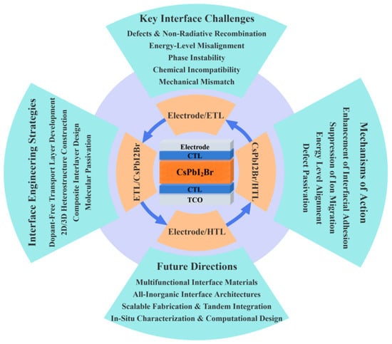
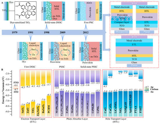
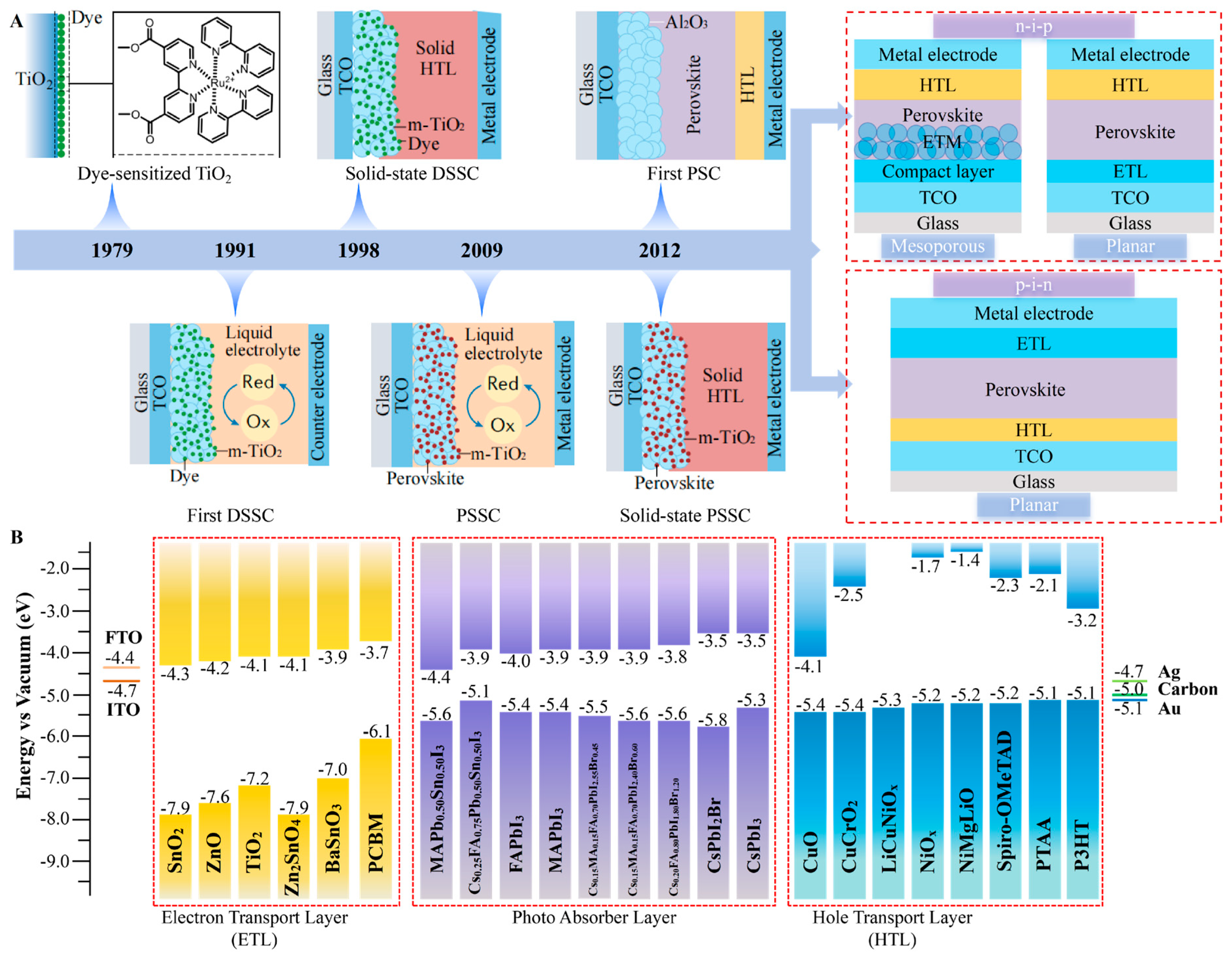
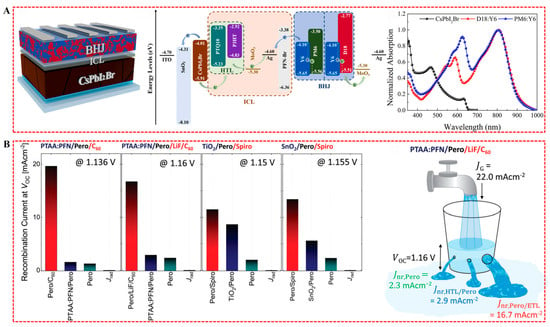
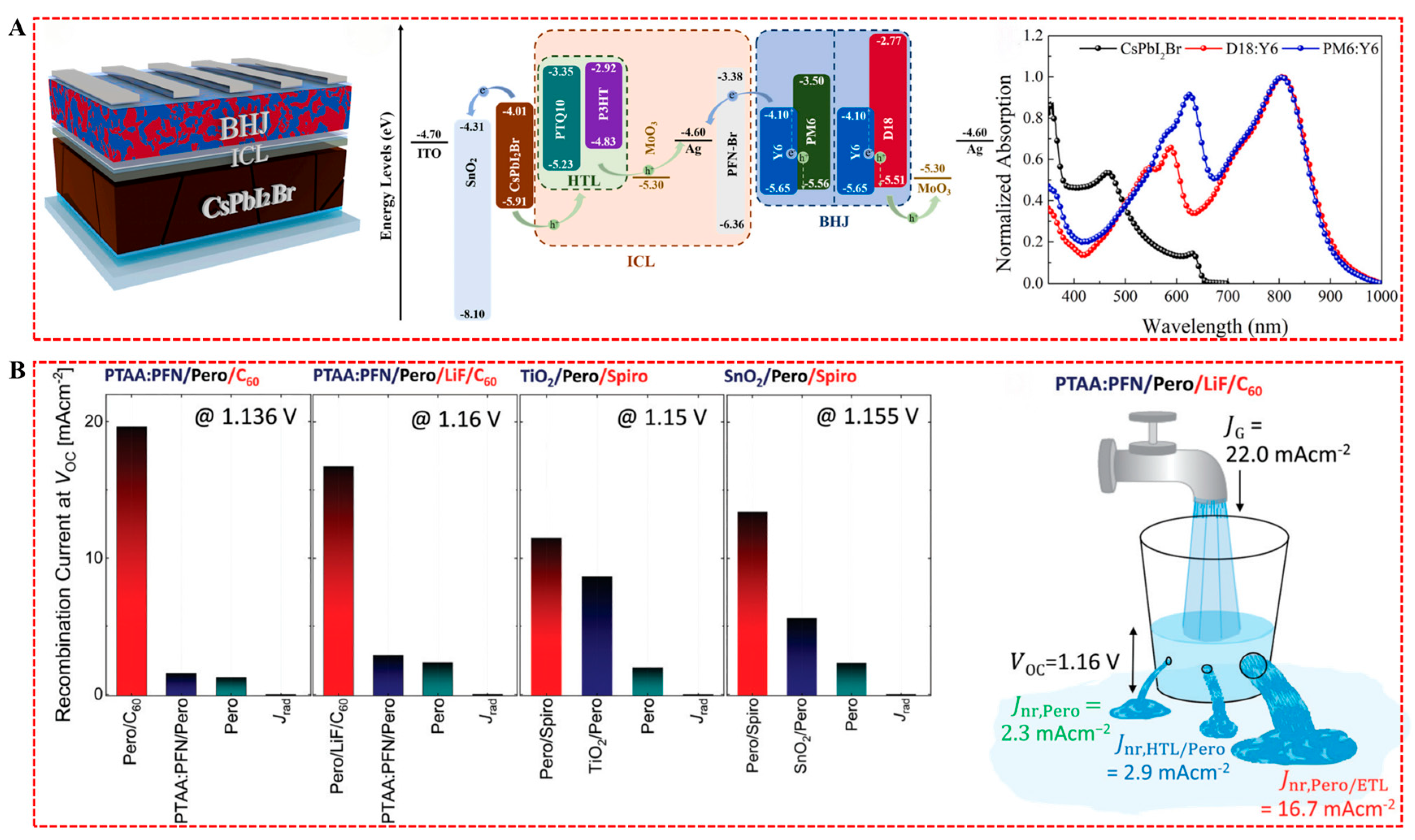
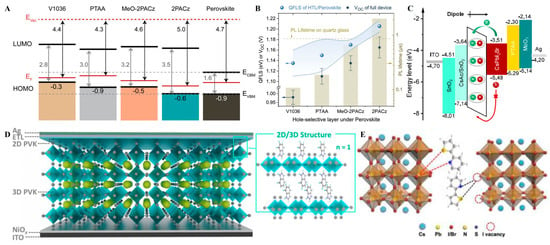
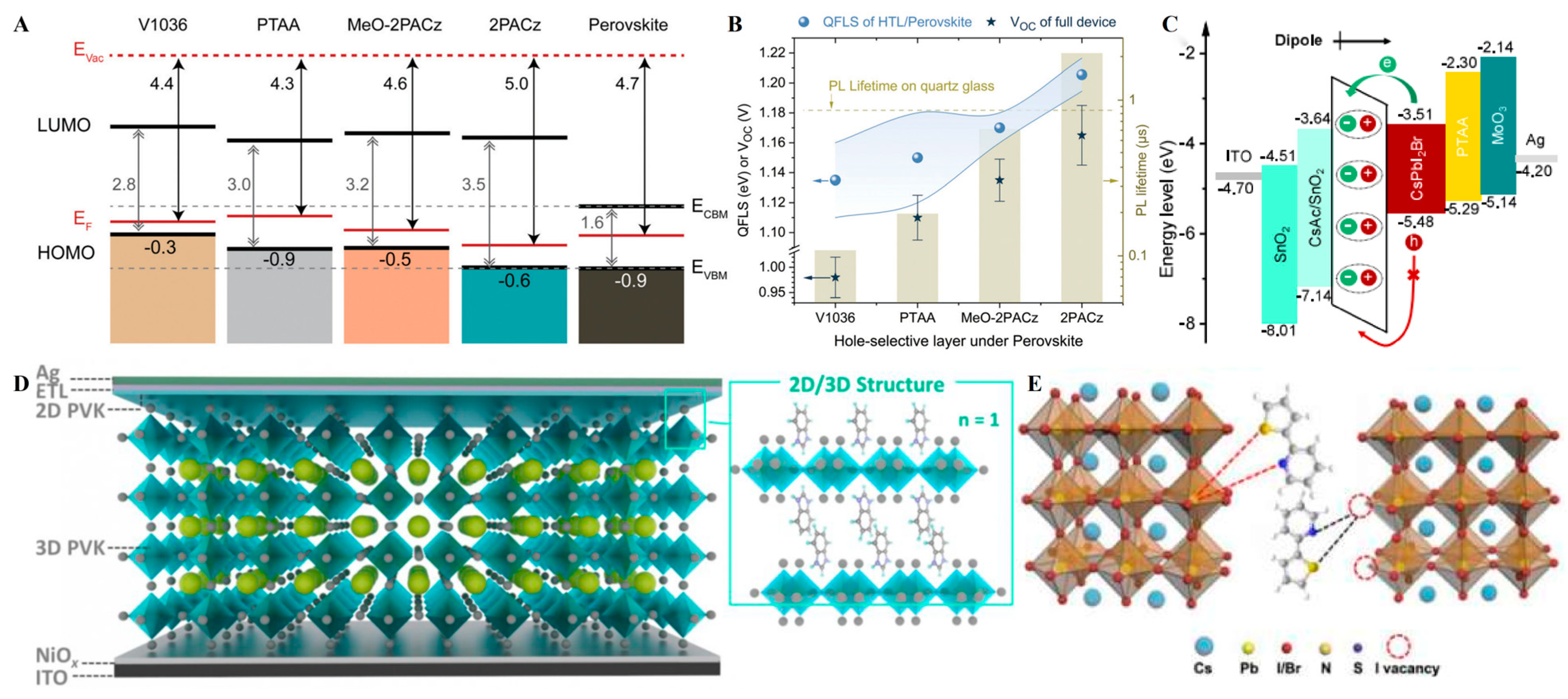
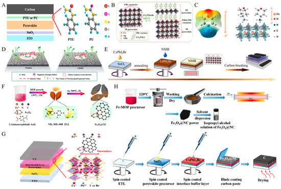
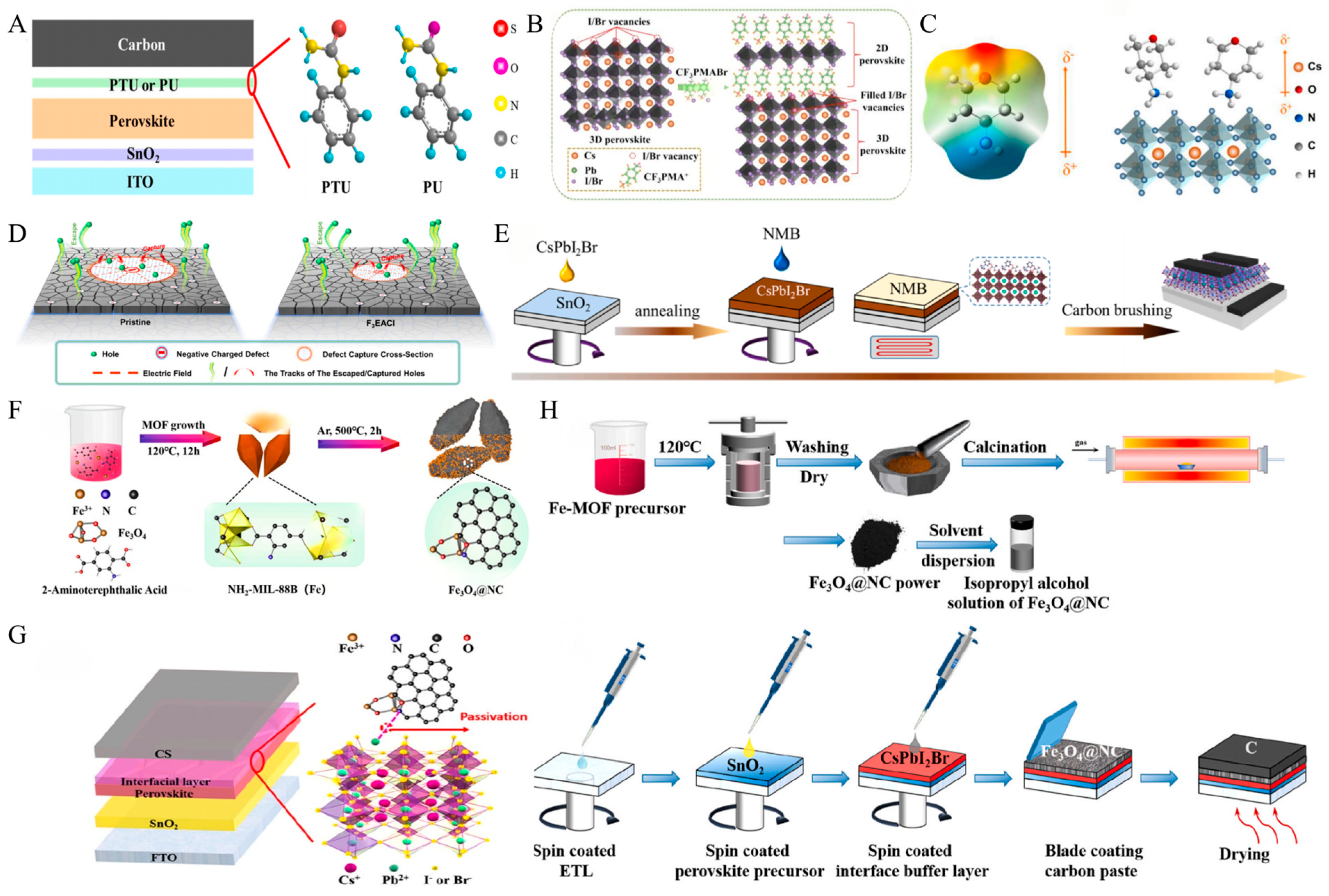
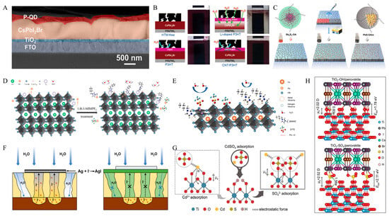
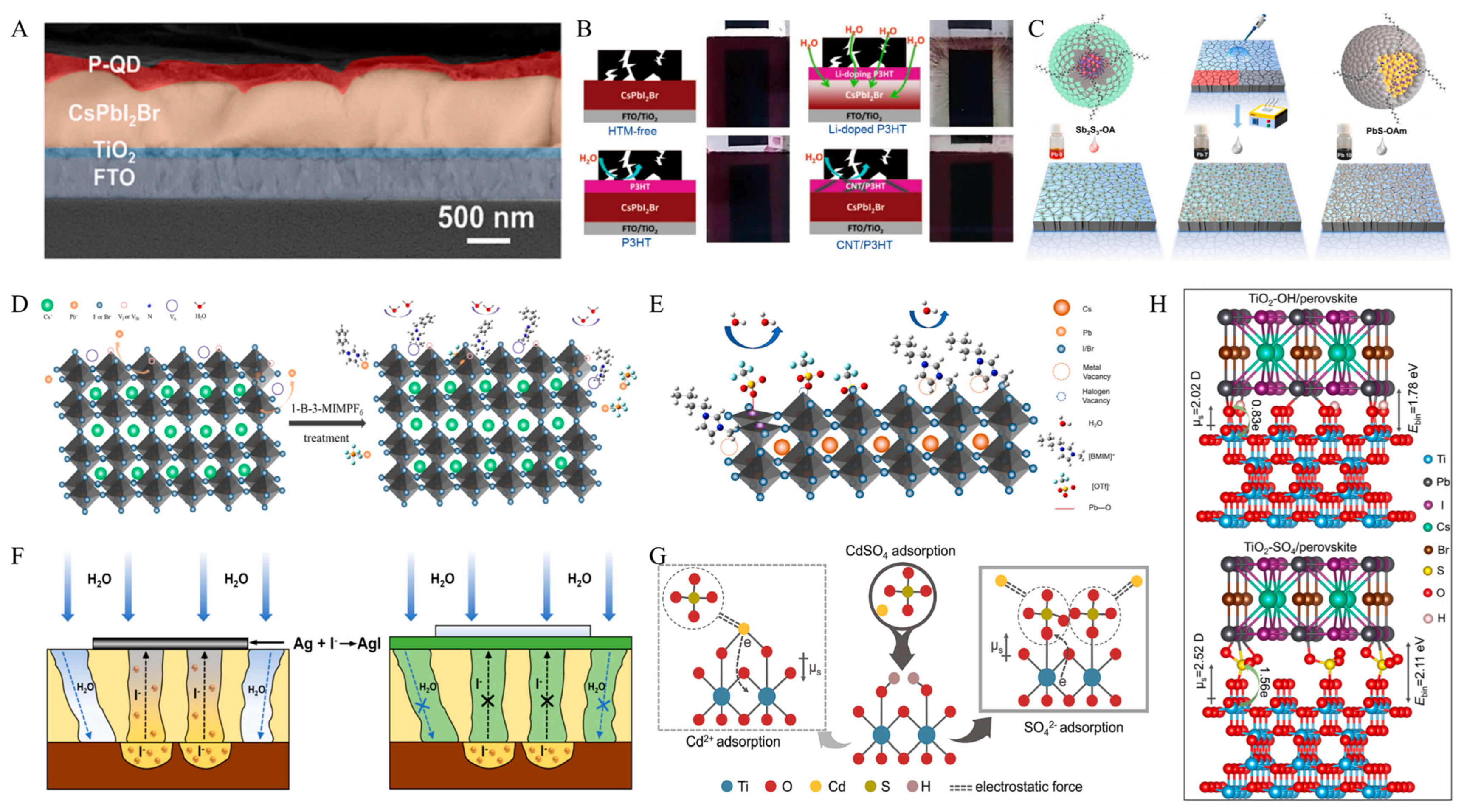
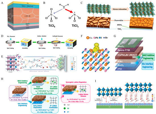
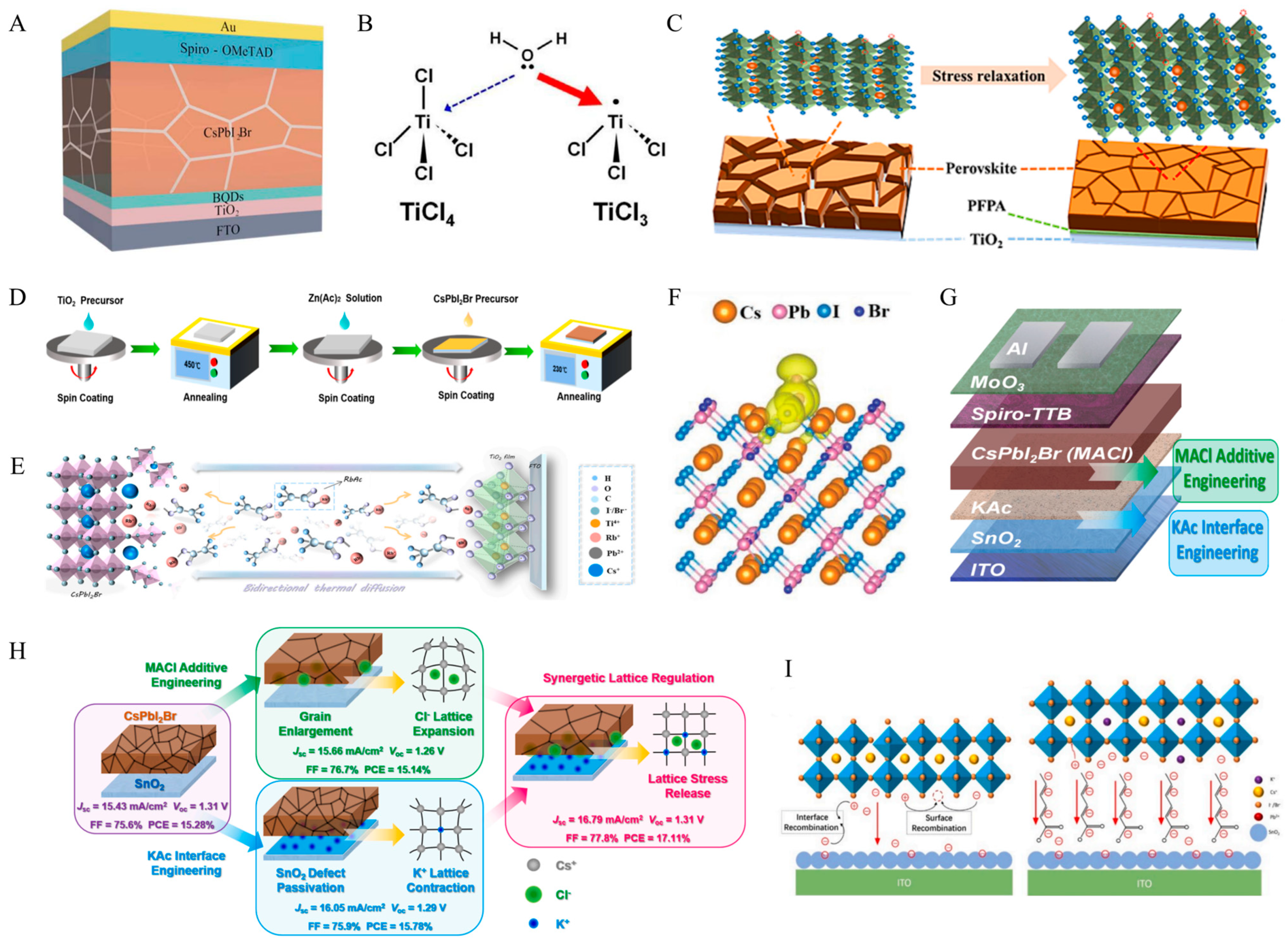
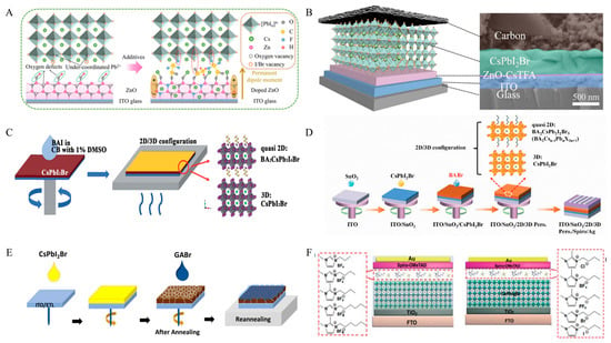
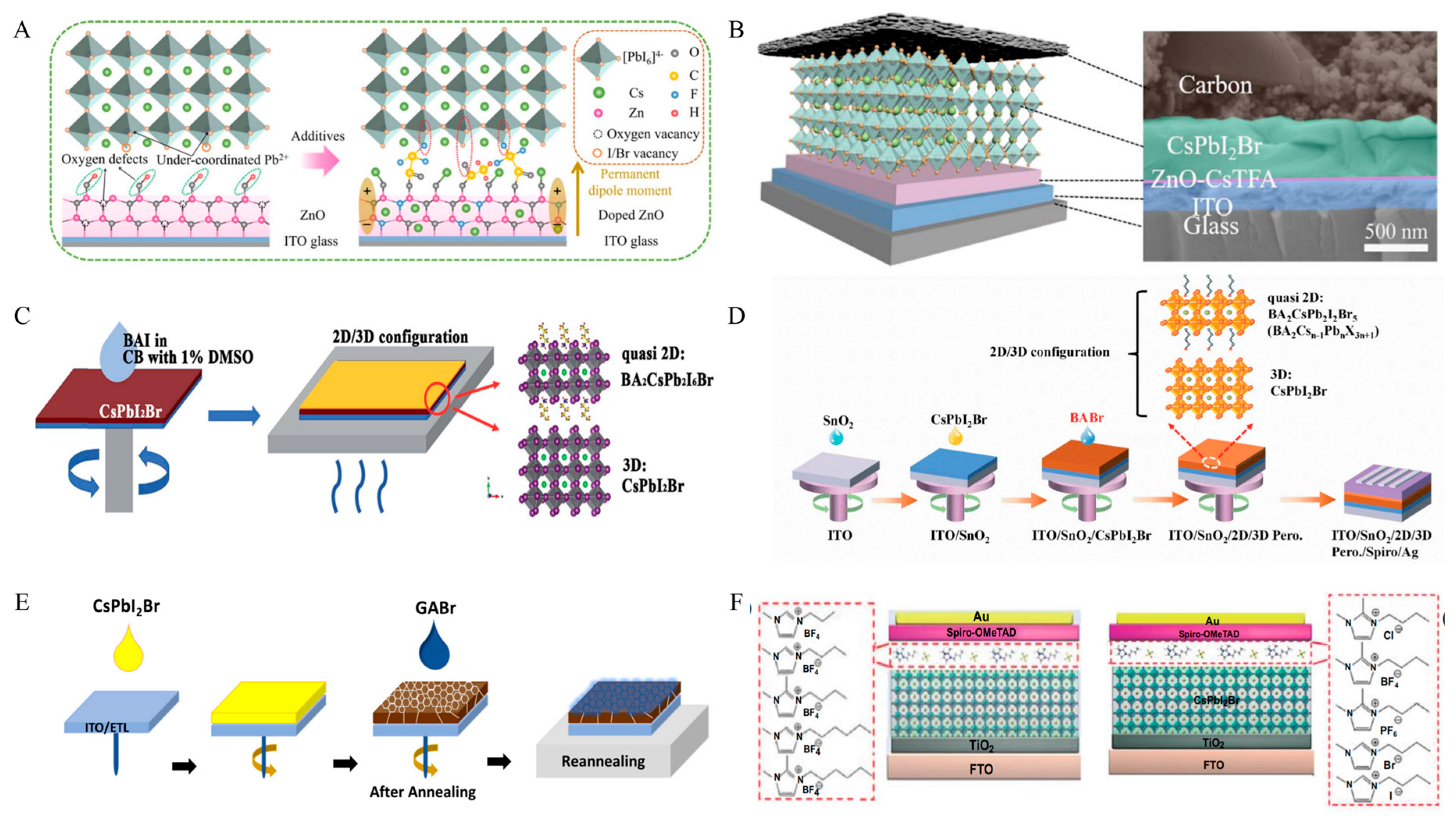
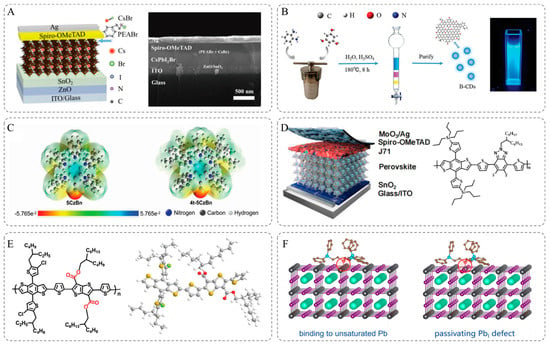
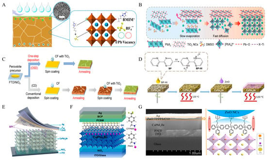
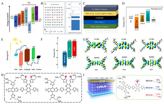
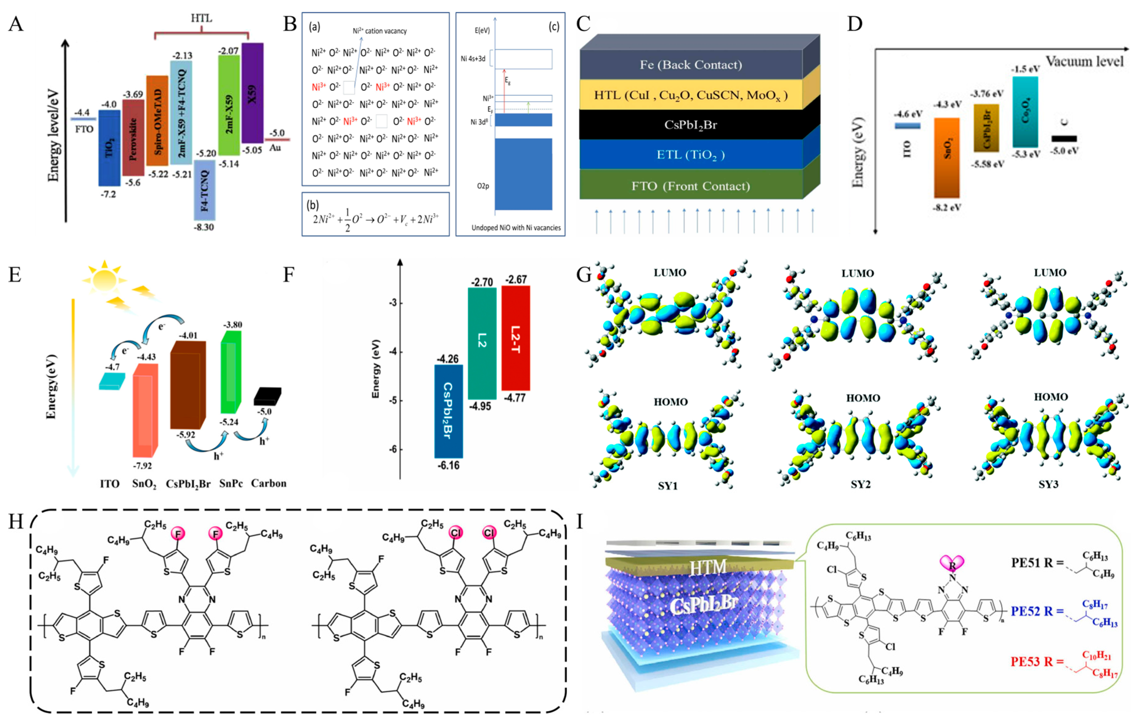
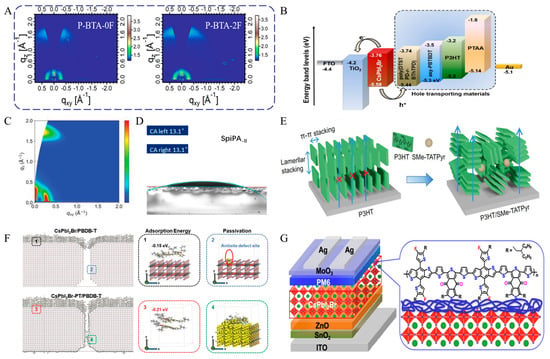
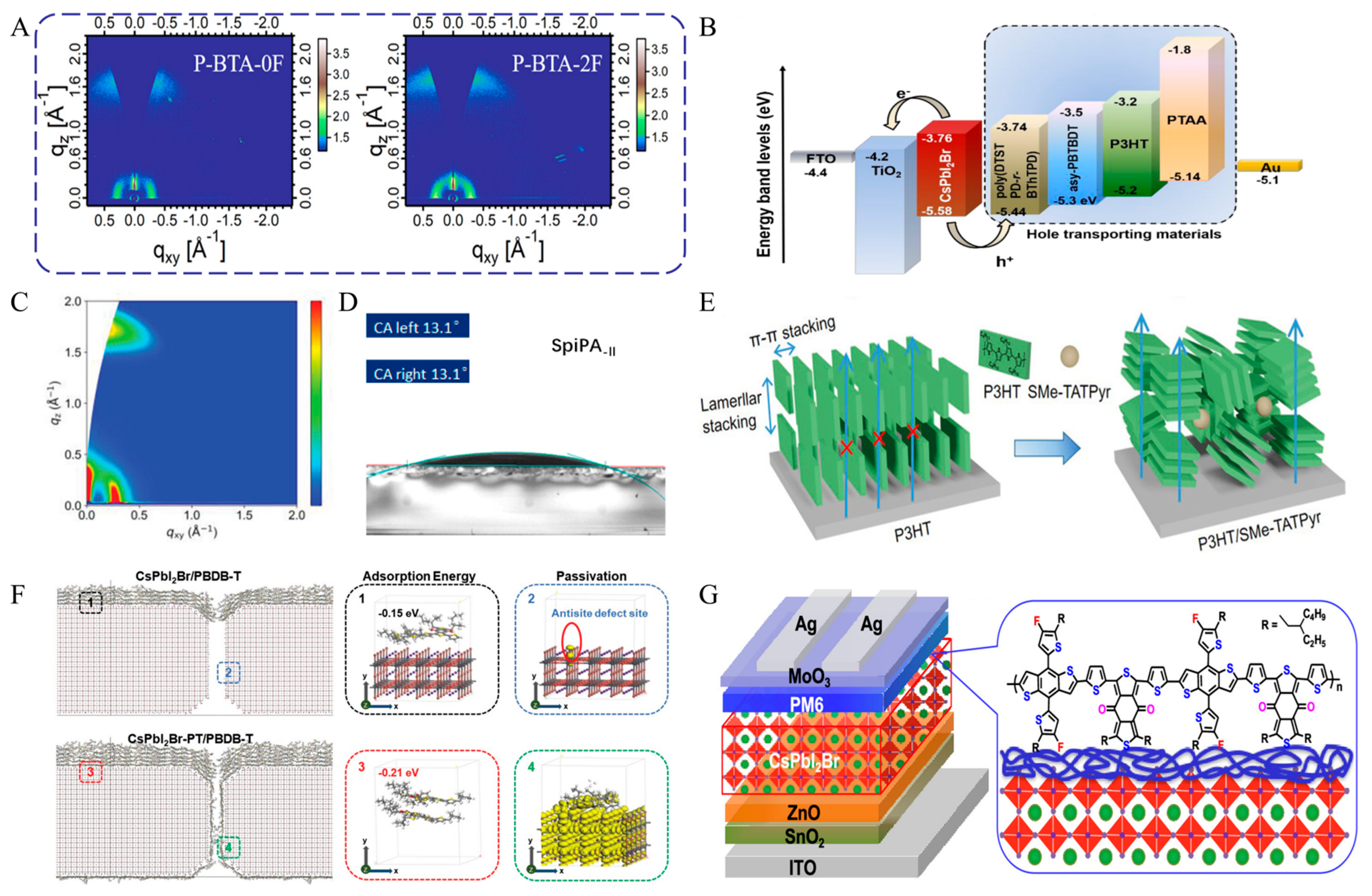
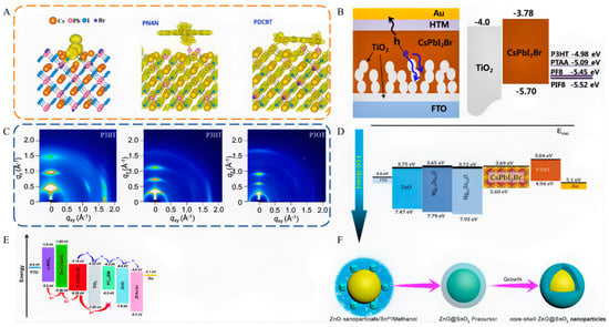
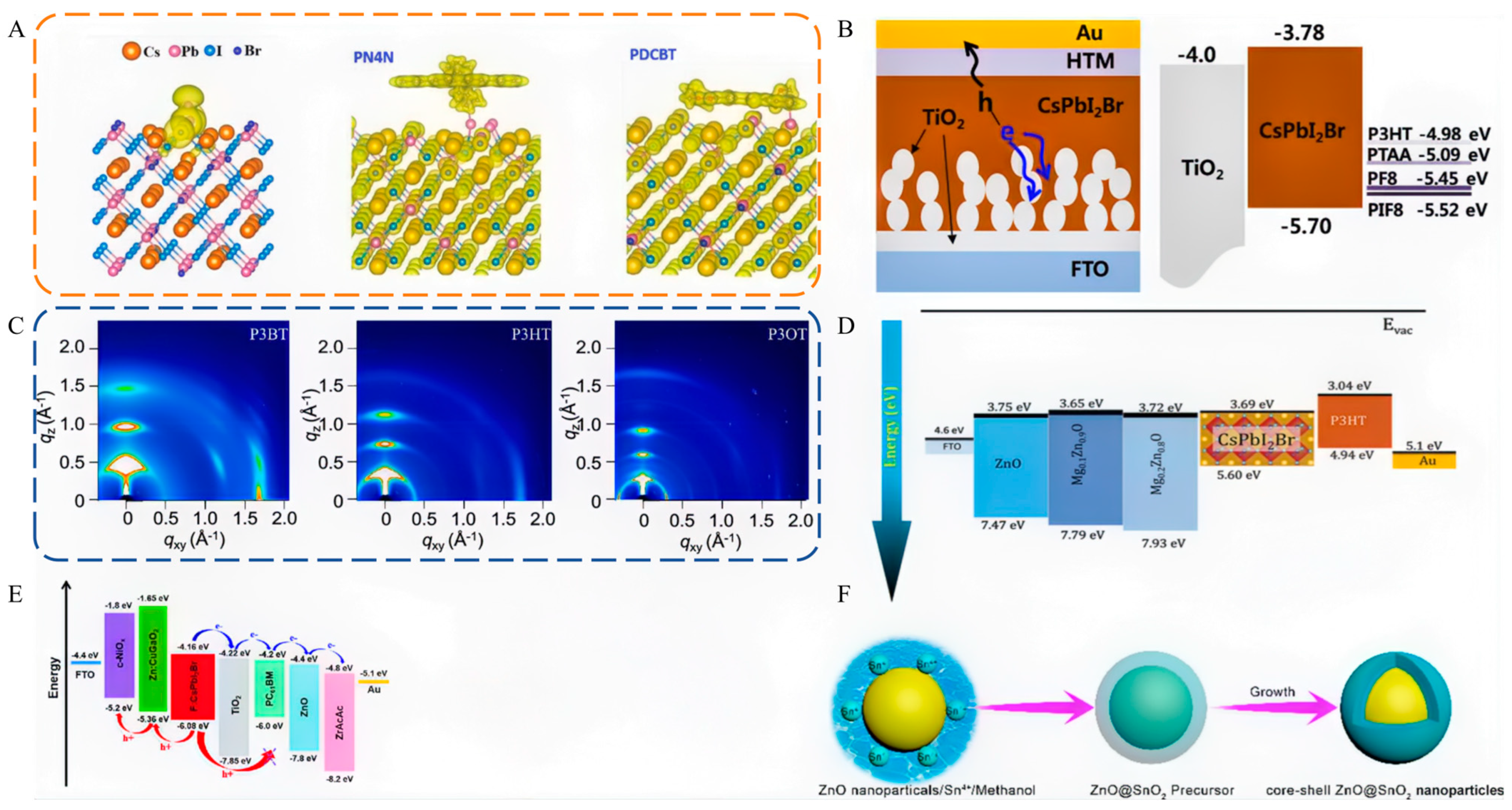
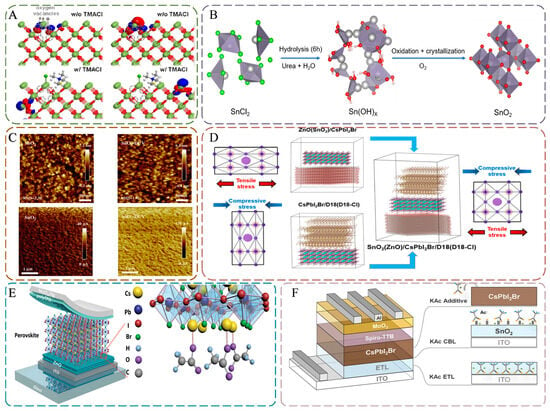
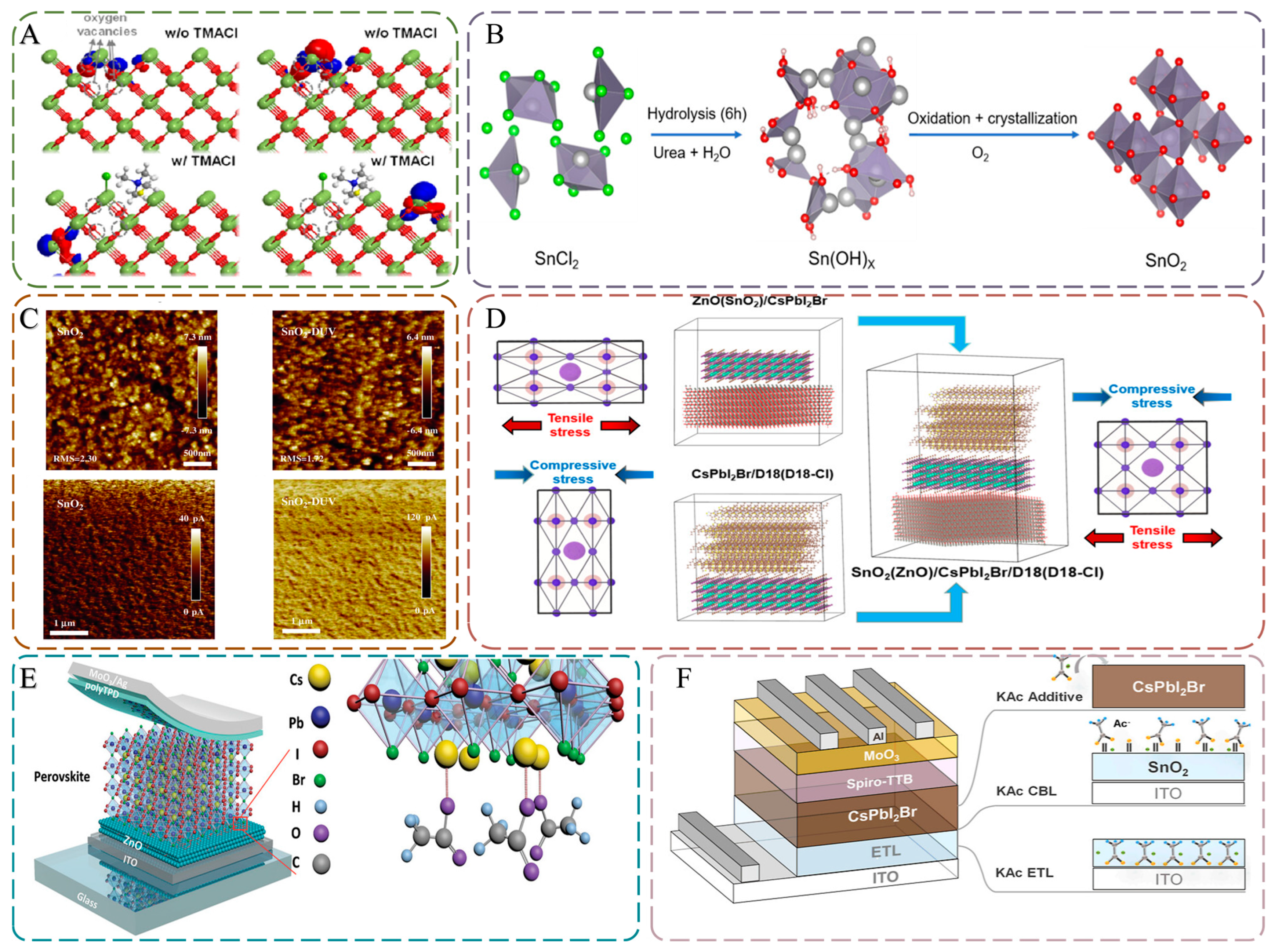

Disclaimer/Publisher’s Note: The statements, opinions and data contained in all publications are solely those of the individual author(s) and contributor(s) and not of MDPI and/or the editor(s). MDPI and/or the editor(s) disclaim responsibility for any injury to people or property resulting from any ideas, methods, instructions or products referred to in the content. |
© 2026 by the authors. Licensee MDPI, Basel, Switzerland. This article is an open access article distributed under the terms and conditions of the Creative Commons Attribution (CC BY) license.