Article

Characteristics of Microsecond-Pulse Source for Atmospheric Pressure Helium Plasma Jet

School of Physics, Beijing Institute of Technology, P.O. Box 327, Beijing 100081, China
*
Author to whom correspondence should be addressed.
Plasma 2026, 9(2), 19; https://doi.org/10.3390/plasma9020019
Submission received: 8 May 2026 / Revised: 25 May 2026 / Accepted: 28 May 2026 / Published: 2 June 2026
(This article belongs to the Special Issue Processes in Atmospheric-Pressure Plasmas—2nd Edition)

Abstract

In this work, based on a half-bridge circuit and pulse transformer, a miniaturized and low-cost microsecond high-voltage pulsed power supply for the atmospheric pressure plasma jet (APPJ) is designed. Because of the low bus voltage of the half-bridge circuit, low-voltage switches can be chosen by the power supply. The characteristics of the output high voltage of the power supply are studied. The experimental results show that uni-polar and bi-polar pulses can be generated by the power supply. The high-voltage pulses have good consistency at different frequencies, and the amplitude of the high-voltage pulse varies approximately linearly with the bus voltage. A needle-ring plasma jet device was driven by the uni-polar pulse of this supply, and the single discharge current pulse can be obtained at the rising edge and falling edge of the high-voltage pulse, respectively. The effects of voltage pulse on APPJ and the characteristics of jet are also investigated. The results show that the plasma jet is only formed at the rising edge of the voltage pulse. The jet length is almost unaffected by the pulse frequency, whereas the normalized intensity of most species increases with frequency linearly.

1. Introduction

Atmospheric pressure plasma jets (APPJs) have attracted much attention in past decades, due to their ability to generate non-thermal plasmas at ambient conditions and adapt to complex-shaped structures [1]. The advantages of APPJ make them suitable for application in many fields, such as biomedicine, materials processing, and nano-material production [2,3,4,5].
Many devices with different configurations were developed to generate atmospheric pressure plasma jets, such as needle-ring, dielectric barrier discharge (DBD) and micro-hollow cathode devices [6,7,8,9]. Helium, argon, nitrogen, air, etc., can be used as the working gases of APPJs. In general, direct current (DC), alternating current (AC), pulsed DC, radio frequency (RF) and microwaves can be adopted to drive some jet devices [10,11,12,13,14]. However, the application of plasma jets in biomedicine requires better tuning of the dosage of reactive species [15]. It is difficult to control the discharge and the generation of the plasma accurately by DC or continuous wave power source. Pulse waveform or continuous wave tailoring are proposed to regulate the discharge plasma of APPJs [15,16,17,18,19,20]. Ivankov et al. compared bipolar short-pulse (BSP) supply and series resonant inverter (SRI) supply for driving the plasma jet of the DBD system; their results show that the voltage waveform can strongly affect the jet characteristics [21]. Some works also used dual-frequency excitation or pulse modulated microwave to improve the jet performance [22,23]. Dual-frequency RF, kHz-RF, or pulsed microwaves increase the complexity of the power supply or circuit.
Pulsed discharges are considered suitable for producing high-energy electrons, which can enhance ionization and excitations. Therefore, they offer better control of the plasma parameters in APPJs, such as electron density, temperature, and reactive species production. According to the pulse width, the power supply is usually divided into nanosecond (ns) pulse and microsecond (μs) pulse sources. Laroussi and Lu used ns high-voltage pulses to produce a cold atmospheric helium plasma jet, which can make contact with human skin safely [9,24]. After that, more works focused on the nanosecond pulsed APPJs. Walsh and Kong demonstrated stable argon and air ns pulsed plasma jets at atmospheric pressure [25,26]. They found that even with air, the average power of the discharge can be lower than 1 W, which is suitable for portable plasma jets [26]. Jiang et al. revealed the effect of pulse polarity on the dynamics of jets and found lower power consumption around 0.2 mJ per pulse [27]. Using ns pulsed supplies, more configurations of APPJs were developed, such as a compact plasma “gun” with a length of up to 50 cm, or a 3D multi-microhole plasma jet [28,29]. The mechanism, characteristics and effects of ns APPJs are also investigated [30,31,32,33].
Although ns pulsed APPJ has many advantages, it requires a nanosecond pulsed power supply with good performance. Some studies used commercial ns pulsed sources, which are relatively expensive. The reason for the high price is mainly the requirement of high-voltage fast switches and complex control circuits to achieve both a high voltage and fast response [34]. Some researchers designed homemade ns pulsed sources, but the operating frequencies of these sources are lower, typically less than 10 kHz [34,35]. Although the length and the efficiency of the plasma jet with the microsecond pulsed source are not as good as that of the ns pulsed source [36,37], the configuration of the μs pulsed source can be simpler and more compact, which is beneficial for the implementation of the portable power supply [38,39]. Some studies have shown that the μs pulse is short enough to optimize the parameters of APPJs [40]. Moreover, the μs pulsed source produces less electromagnetic interference, which is helpful to reduce the electromagnetic compatibility problems of the power supply and the experimental measurement system [41].
Many researchers have devoted themselves to the development of micro-second pulse generators for gas discharge. Lots of the μs pulsed power supplies are based on the flyback topology, which uses the single IGBT/MOSFET element and a pulse transformer as an energy storage inductor (also a voltage amplification element) [38,39]. However, the output waveform quality of this kind of supply is poor. Jin et al. proposed a RDD (resistor–diode–diode) circuit at the secondary side of pulsed transformer to shape the output pulse, which allows for the flexible load matching for different DBD structures [41]. They also developed a microsecond pulse module powered by a lithium battery [42]. Although the μs pulsed sources of flyback topology are simple and compact, the output waveform may change with voltage [38]. And the operating frequencies of the power supply with inductive energy storage are also limited to less than 10 kHz [38,39,41,42]. The applications of APPJs need a wider driving frequency range to adjust the number of reactive species. In this paper, a compact microsecond pulsed power supply is implemented by using a half-bridge circuit and pulsed transformer. Since energy storage in the inductor is not required, there is no need for an air gap in the transformer core as in a flyback configuration. And unipolar or bi-polar waveforms can be generated by this source. A simple shaping circuit is also designed at the primary side of the pulsed transformer to obtain a better output waveform. The output waveform and power consumption of the power supply under different conditions are investigated. And the characteristics of the needle-ring helium plasma jet driven by this μs pulsed source are studied.

2. μs Pulsed Source and Experimental Setup of APPJ

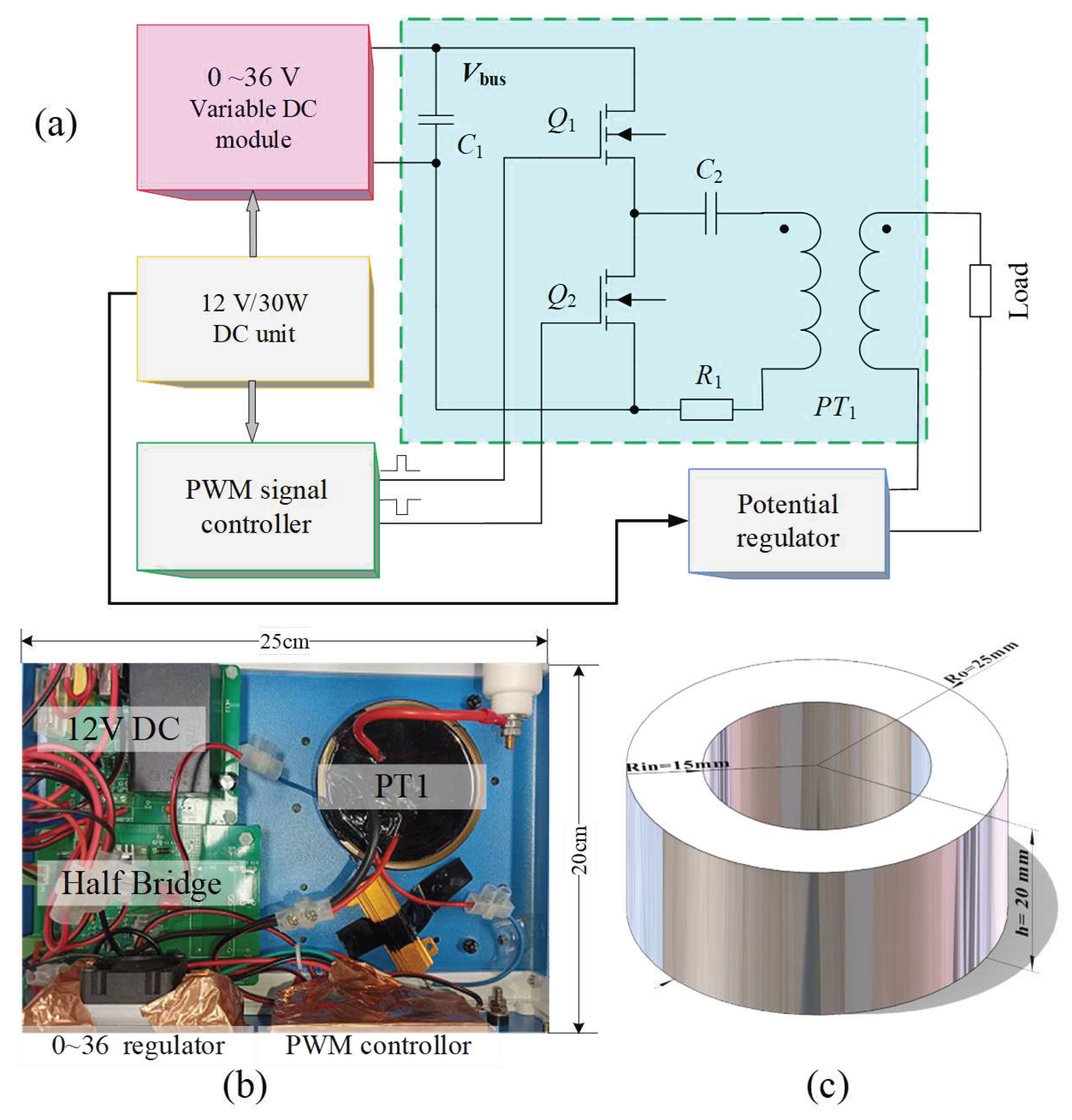
Figure 1a,b show the schematic diagram and the photo of the μs pulsed source, respectively. The main part of the source includes a half-bridge circuit and a home-made pulse transformer ( P T 1 ). P T 1 uses a toroidal ferrite core with an inner diameter of 15 mm, an outer diameter of 25 mm, and a height of 20 mm, as shown in Figure 1c. The turns ratio of the pulse transformer P T 1 is 1:100.
The half-bridge circuit is composed of two MOSFETs Q 1 and Q 2 (FQP10N60C). A 12 V, 30 W DC unit provides power for the whole μs pulsed high-voltage generator. Through a variable voltage module, the output of the 12 V DC unit is converted to 0∼36 V bus voltage ( V bus ) as the energy supply of half-bridge circuit. The 12 V DC unit is also used to power the pulse-width modulation (PWM) signal controller. The controller can generate driving signals for the two MOSFETs of half-bridge circuit with the variable duty ratio. When Q 1 is ON and Q 2 is OFF, a current pulse passes through the primary coil of the transformer P T 1 . The energy is transferred to the secondary coil, and a high-voltage pulse on the APPJ device will be obtained. The frequency of the high-voltage pulse can be up to 20 kHz. The capacitor C 2 is used to avoid short circuit after the core of the transformer becomes saturated. The resistor R 1 is connected in series with the primary side of P T 1 as a damping resistor to obtain better waveforms.
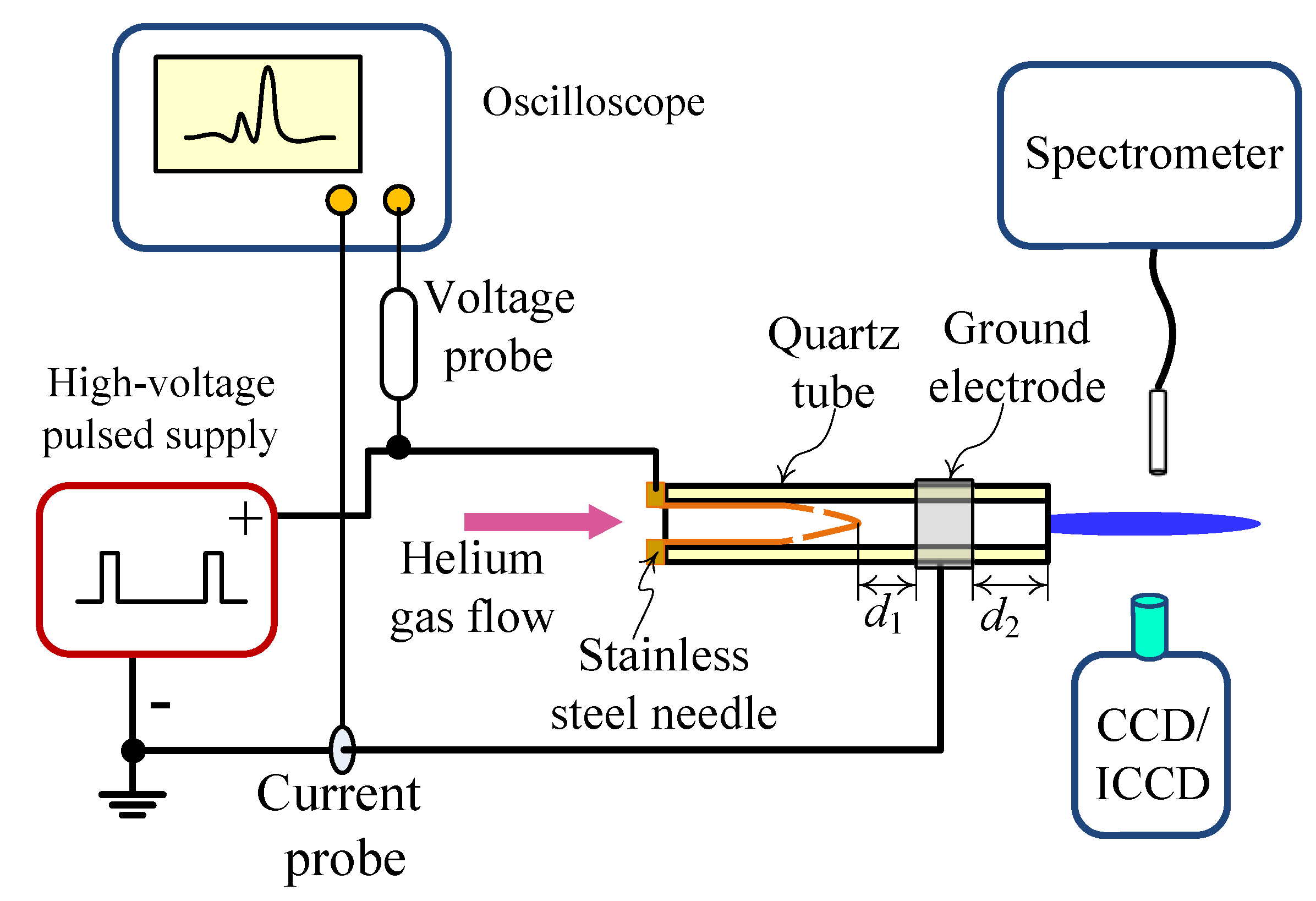
Because of C 2 in the half-bridge circuit, a DC offset will be formed between discharge electrodes. Therefore, a potential regulator is adopted at the secondary coil to adjust the DC offset. The power supply is compact and accommodated in the case of 25 × 20 × 12 cm. Because of the low V DC , expensive high-voltage MOSFET is not needed by the half-bridge circuit, which can greatly reduce the cost of the whole power supply. The APPJ device has a typical needle-ring DBD configuration, as shown in Figure 2. A hollow stainless steel needle, 34 mm in length and 1.6 mm in diameter, is used as the high-voltage electrode and connected to the output of the pulse generator. The needle is inserted into a quartz tube with an inner diameter of 2 mm and an outer diameter of 3 mm. A metal ring is wrapped around the quartz tube as a ground electrode. The width of the metal ring is 2 mm. The distance d 1 between the tip of the stainless steel needle and the edge of the metal ring is 5 mm. And the distance d 2 between the edge of the metal ring and the outlet of the quartz tube is 10 mm.
High purity helium flow (Beijing AP BAIF Gases Industry Co., Ltd. (Beijing, China), 99.999%) is injected into the discharge channel through the needle, and the flow rate is controlled by a gas flow-meter (Sevenstar CS200, Beijing Sevenstar Flow Co., Ltd., Beijing, China). The voltage applied on the needle is monitored by a high-voltage probe (P6015A, Tektronix, Inc., Beaverton, OR, USA). The discharge current on the grounded electrode is measured by a current probe (Pearson 2877, Pearson Electronics, Inc., Palo Alto, CA, USA). The voltage and current waveforms are observed and saved by a digital oscilloscope (DPO 4034B, Tektronix, Inc., Beaverton, OR, USA). The time-integrated images of the plasma jet are recorded by a CCD camera (D7200, Nikon Corporation, Tokyo, Japan), and the time-resolved images are acquired by an intensified charge-coupled device (ICCD) camera (iStar DH334T, Andor Technology Ltd., Belfast, UK) with kinetic series mode. A fiber is placed about 5 mm away from the outlet of the quartz tube and perpendicular to the jet to guide the light into a spectrometer (AvaSpec-ULS3648, Avantes B.V., Apeldoorn, The Netherlands), which can capture the optical emission spectra (OES) of the plasma jet.

3. Characteristics of the μs Pulsed Source

3.1. Simulation of the Circuit

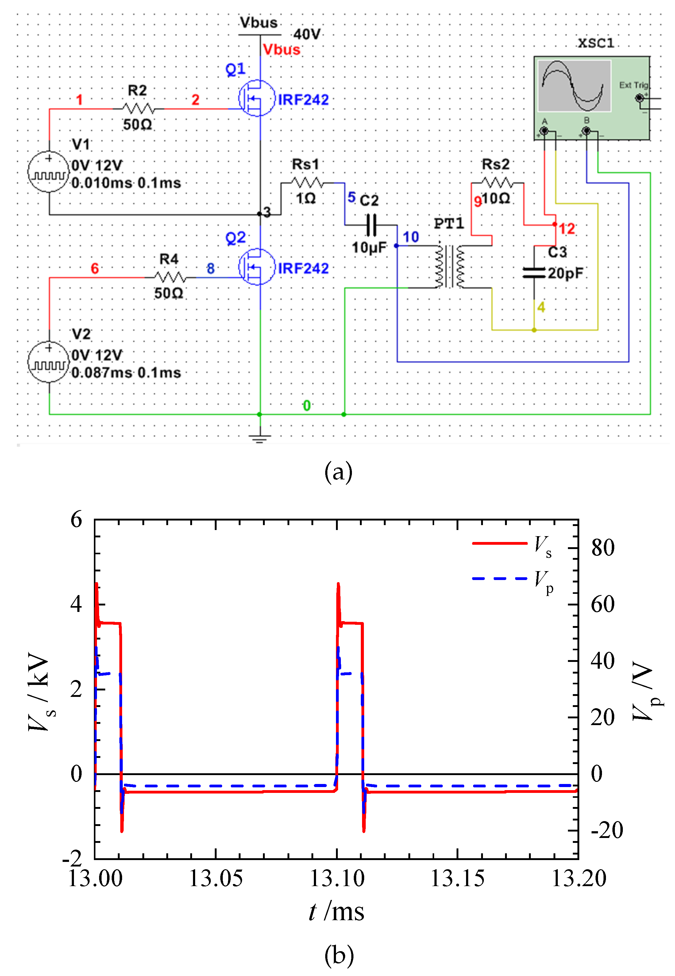
Before the experiments, a circuit model of the μs pulsed source was built and simulated by Multisim. Figure 3a shows the schematic of simplified circuit model. In the simulation, the pulse transformer is modeled by an ideal transformer, and the turns ratio of the primary coil to the secondary coil is 1:100, which is equal to that of the self-made transformer in our experiments. The potential regulator at the secondary side is omitted. Resistors R s 1 and R s 2 in the figure are approximate values of stray resistances in the primary and secondary circuits. The load capacitance is set to be 20 pF, encompassing the capacitance of the needle-ring APPJ device, P6015 high-voltage probe capacitance, and stray capacitance of the circuit.
Figure 3b shows the results obtained by simulation. The red solid curve and the blue dashed curve show the waveforms of secondary coil V s and primary coil V p , respectively. In the model of Figure 3a, the bus voltage V bus is 40 V; the width and the period of the driving pulse for Q 1 are 0.01 ms and 0.1 ms, respectively. As can be seen from Figure 3b, a 10 kHz high-voltage square wave pulse with overshoots at the rising and falling edges is generated by the circuit. Without the overshoots, the peak-peak value of the voltage is about 4 kV, which corresponds to 100 times amplification of V bus . In the experimental circuit, due to the influence of stray parameters in the circuit, there are more oscillations in the input and output waveforms, so the damping resistor R 1 (see Figure 1) is connected in series with the primary side of the transformer to suppress the oscillation. Because the potential regulator is omitted, it can be seen from the the waveforms in Figure 3b that there is a negative DC offset between the two positive pulses. Therefore, using the voltage regulator of the secondary circuit, unipolar or bipolar square waves can be obtained by this μs pulsed source.

3.2. Output Waveforms in Experiments

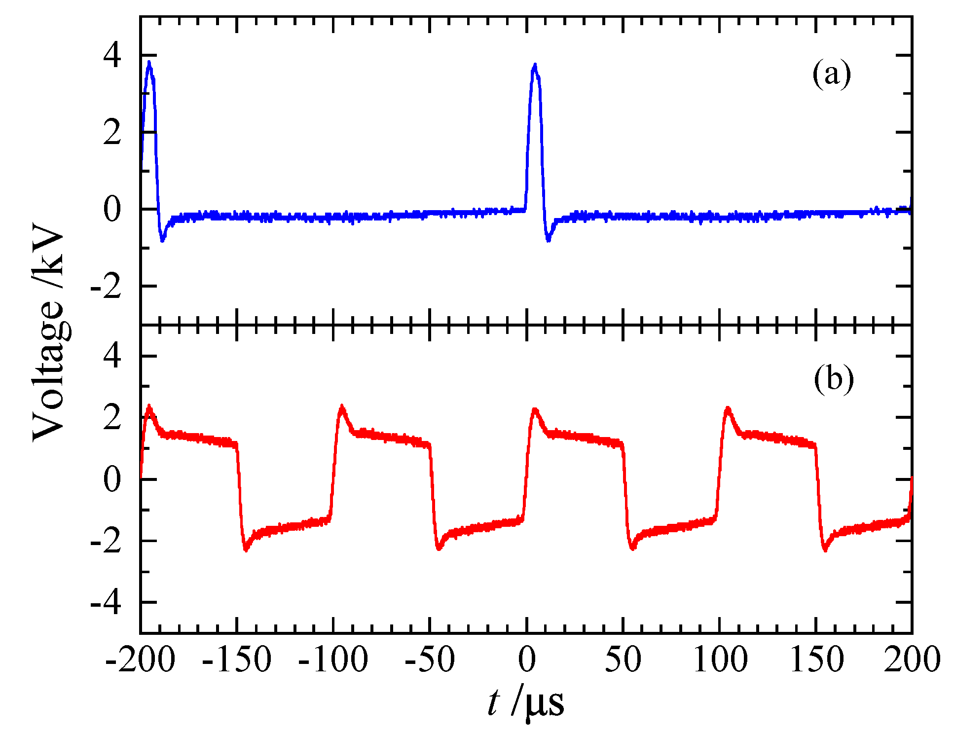
Figure 4 presents two different voltage waveforms output by the pulsed power supply without discharge. Figure 4a,b show uni-polar pulses at 5 kHz and bi-polar pulses at 10 kHz, respectively. This indicates that the designed μs pulsed supply can generate a quasi-square wave with different types and frequencies, and the pulse width is also adjustable. Compared with the simulation results in Figure 3, it can be seen that the overshoots at the rising and falling edges still exist, but the oscillations are suppressed. In Ref. [21], a full-bridge voltage inverter was used, and the oscillation behavior of the voltage waveform was also observed in the results. This is mainly related to the leakage inductance of the transformer and the capacitive characteristic of the plasma jet device. As can be seen from Figure 4, R 1 indeed has an effect on waveform shaping. However, using the damping resistor is a trade-off solution because excessive damping will reduce the voltage rise rate and result in additional power consumption.
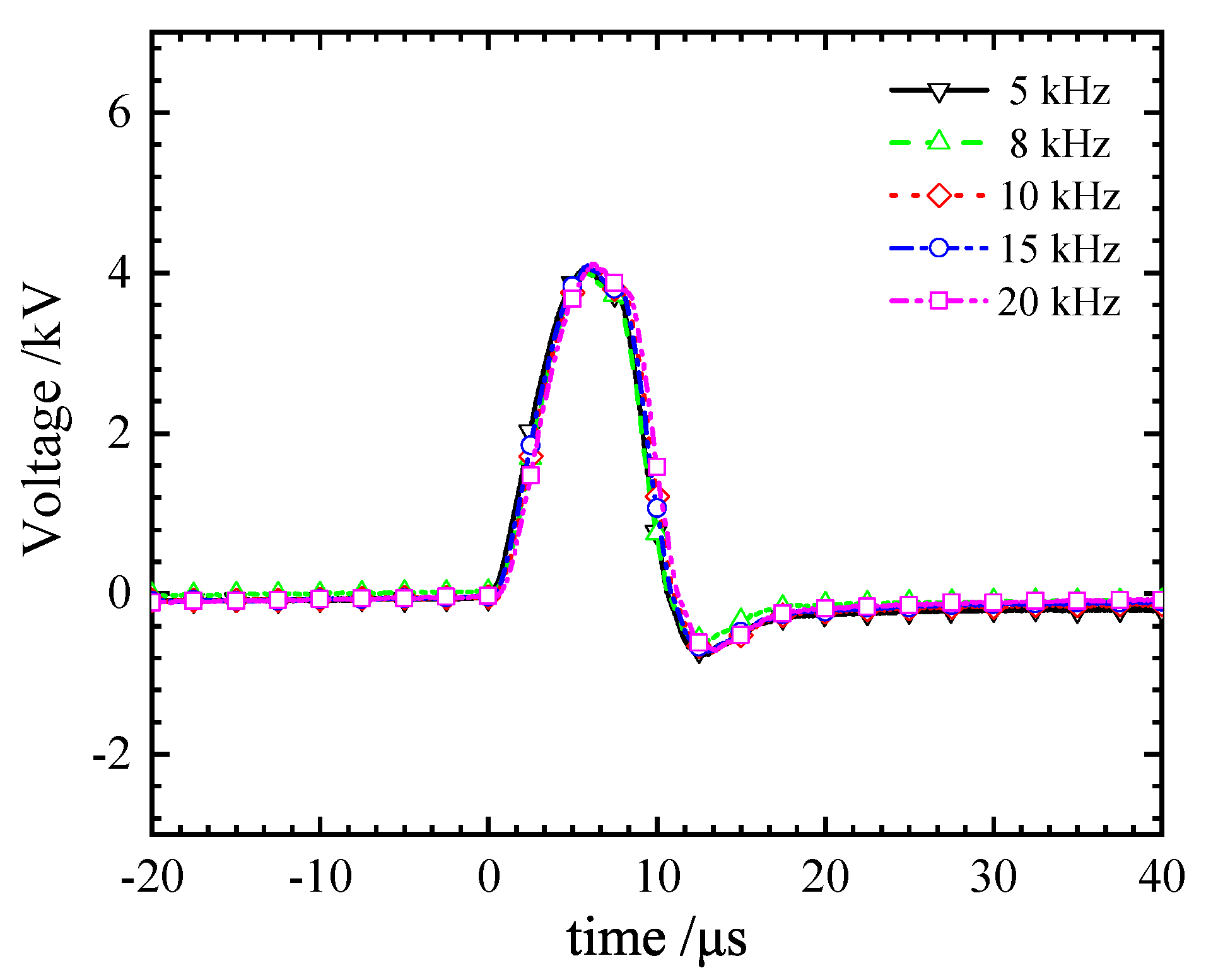
The jet generated by the uni-polar pulse can propagate to a longer distance, so we mainly discuss the experimental results of uni-polar pulse. The waveforms of the uni-polar pulse from 5 kHz to 20 kHz are shown in Figure 5. For all the waveforms, the voltage V bus remains constant at 30 V. It can be seen that the waveforms of pulses under different frequencies nearly coincide. The rising and falling edges of voltage pulses is about 3∼5 μs. The voltage reaches a peak value (about 4 kV) at around 4.5 μs with a small overshoot. After that the voltage declines to a slightly lower value (over 3.6 kV) within 2.5 μs, then drops rapidly in 3 μs to form a negative overshoot. Therefore, the minimum width of output pulse T W can be on the order of 10 μs. The rising and falling edges of the experimental waveform are slower than that of simulation results (Figure 3). It is considered that this phenomena is mainly caused by the leakage inductance and the parasitic capacitance of the transformer. The curves in Figure 5 also show that the output high-voltage pulses are stable at the frequency < 20 kHz. The stability ensures the repeatability of discharge and jet generation in each pulse at different frequencies.
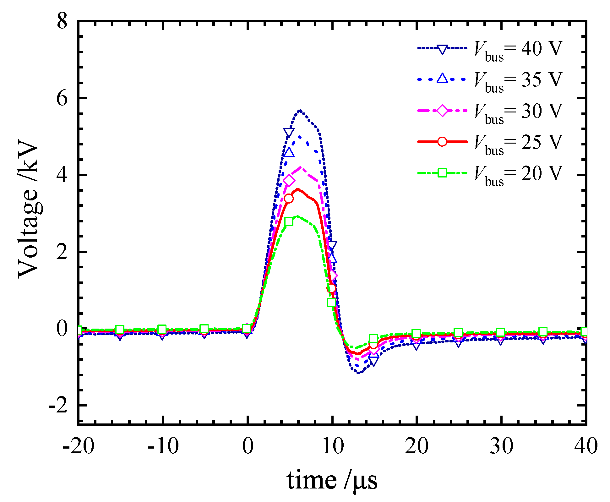
In order to investigate how the performance of the pulsed source varies with V bus , a linear DC power supply is adopted to replace the 0∼36 V variable module of Figure 1 in the following experiments. Therefore, V bus in experiments can be higher than 36 V. Figure 6 shows the output waveforms as V bus increases from 20 V to 40 V. The pulse frequency is kept at 10 kHz. As can be seen from Figure 6, except for the amplitude of high-voltage pulse V amp , that the voltage V bus has almost no impact on the waveform of the high-voltage pulse.

3.3. Power Consumption

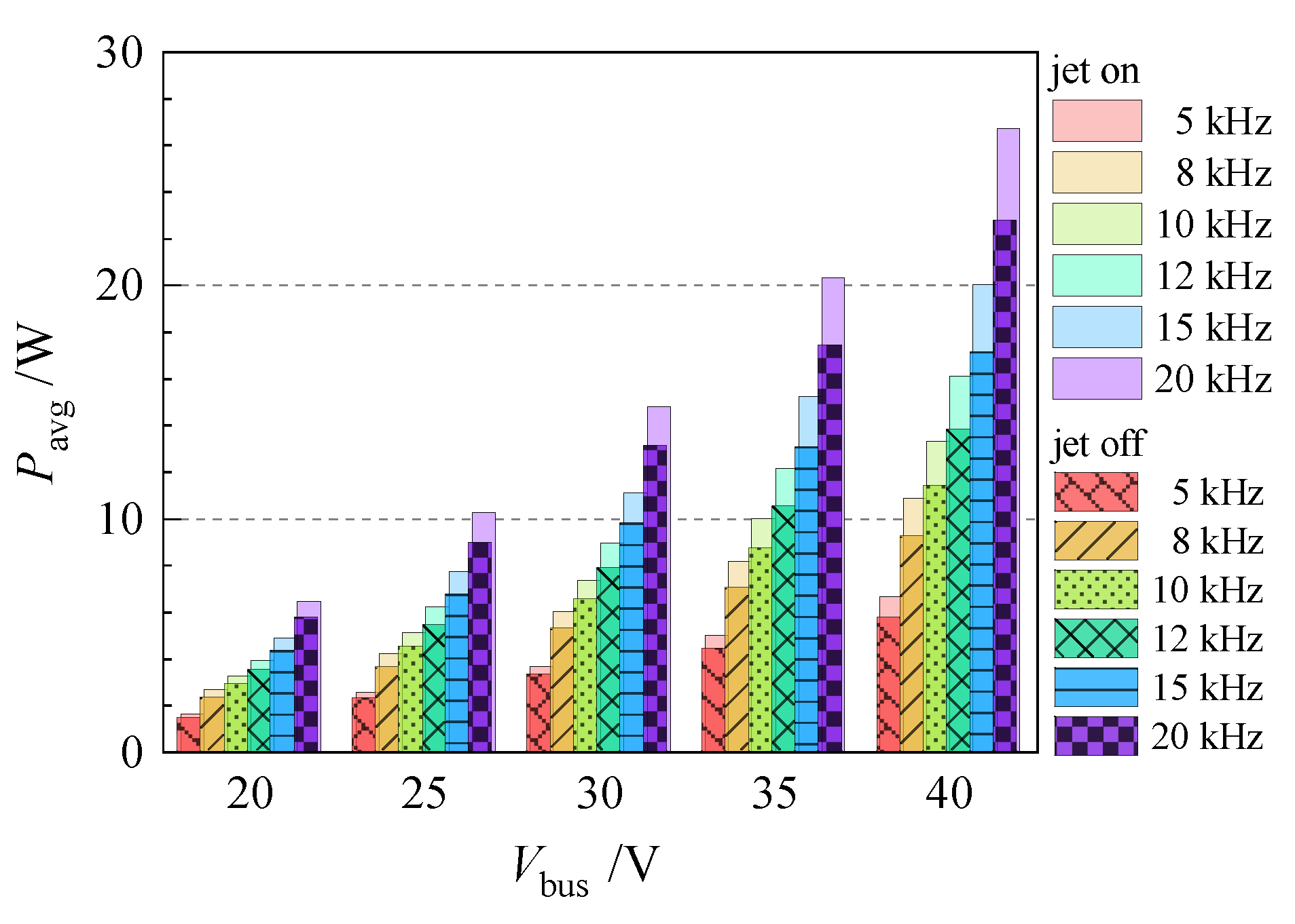
With the linear DC power supply, the average current I avg at different V bus can also be measured. Then the average power consumption P avg of the half-bridge circuit (which is the main energy-consuming part in the entire supply) is obtained by V bus · I avg . Figure 7 presents the experimental data P avg versus V bus during the plasma jet on or off. It is shown clearly that at the same frequency, the average power consumption increases with V bus , regardless of whether the plasma jet is on or off. Similarly, the average power consumption increases with frequency f at the same V bus .
The power consumption by the discharge and the plasma jet is small, which is indicated clearly in Figure 7. At V bus = 40 V and f = 20 kHz, the average power consumptions reach maximum values of 24.4 W (at jet off) and 26.7 W (at jet on), respectively. These values reduce to 1.5 W and 1.6 W at V bus = 20 V, f = 5 kHz. The ratio of energy used for the generation of discharge and plasma jets is less than 10%. It is considered that the energy is consumed mainly in the half-bridge circuit and in the core of the transformer. Therefore, further improvements in energy efficiency will be focused on optimizing the design of half-bridge circuit and the waveform shaping circuit.

3.4. Q–V Lissajous Figure

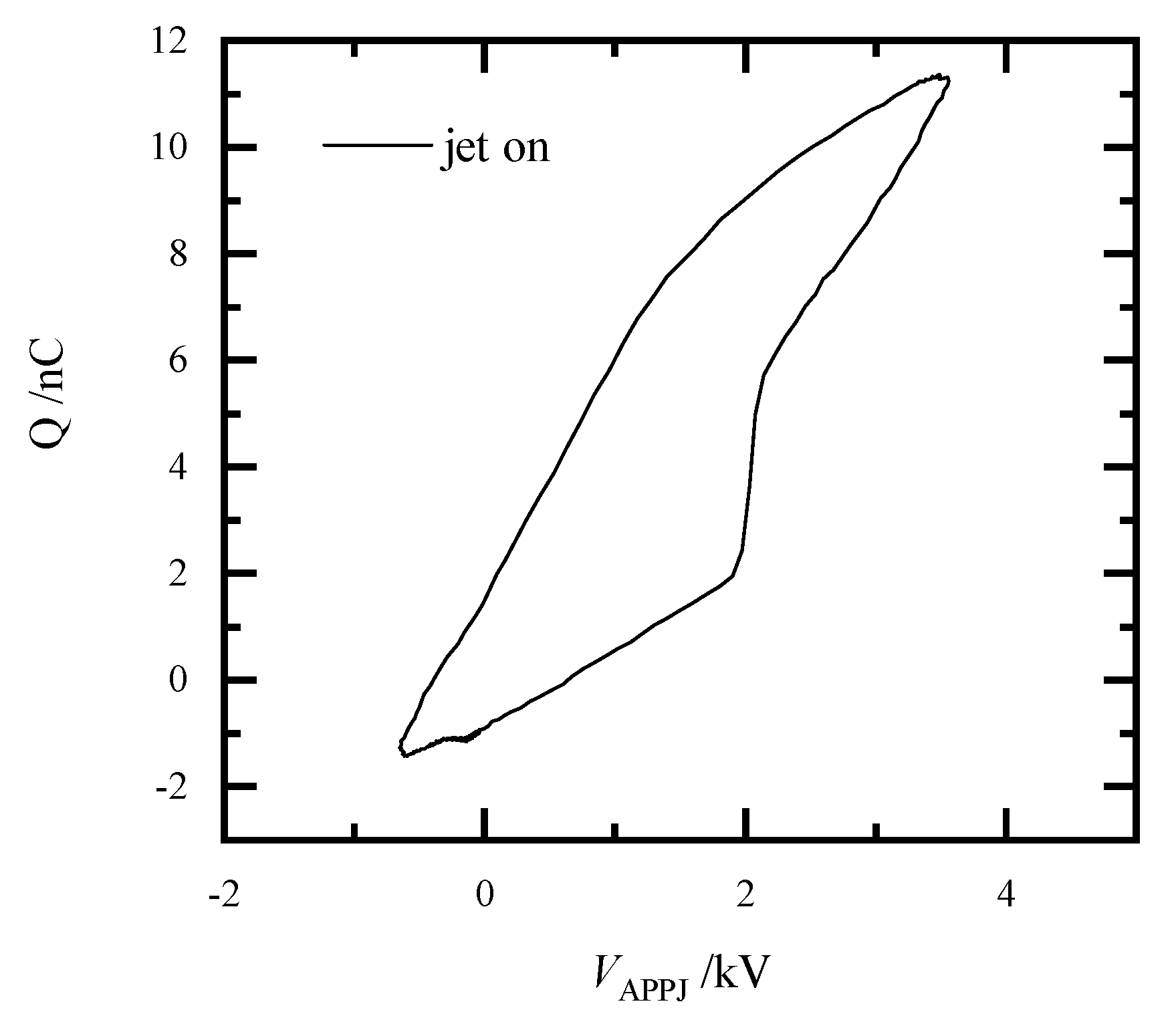
It should be noted that P avg in Figure 7 represents the average input power consumption of the half-bridge circuit, rather than the net power delivered to the plasma. To further evaluate the electrical behavior of the APPJ load, a representative QV Lissajous figure was obtained under V bus = 30 V, f = 10 kHz, and T W = 10  μs, as shown in Figure 8. In the measurement, a sampling capacitor C s = 200 pF was connected in series with the grounded electrode, and the transferred charge was obtained from the voltage across this capacitor:
Q ( t ) = C s V s ( t ) ,
The energy transferred to the load during one period can be estimated from the enclosed area of the Lissajous figure:
E DBD = V APPJ d Q .
The corresponding average discharge power is then given by
P DBD = f E DBD .
For Figure 8, the enclosed area of the QV Lissajous figure is approximately 15 kV · nC , corresponding to a transferred energy of 15 μJ per cycle and an average discharge power of about 0.15 W at f = 10 kHz . The intrinsic capacitance of the APPJ structure was also estimated from the slope of the QV curve during the discharge extinguished, and the value is approximately 1.5 pF.

4. APPJ Driven by μs Pulse

4.1. Effects of V amp and f on Jet Length

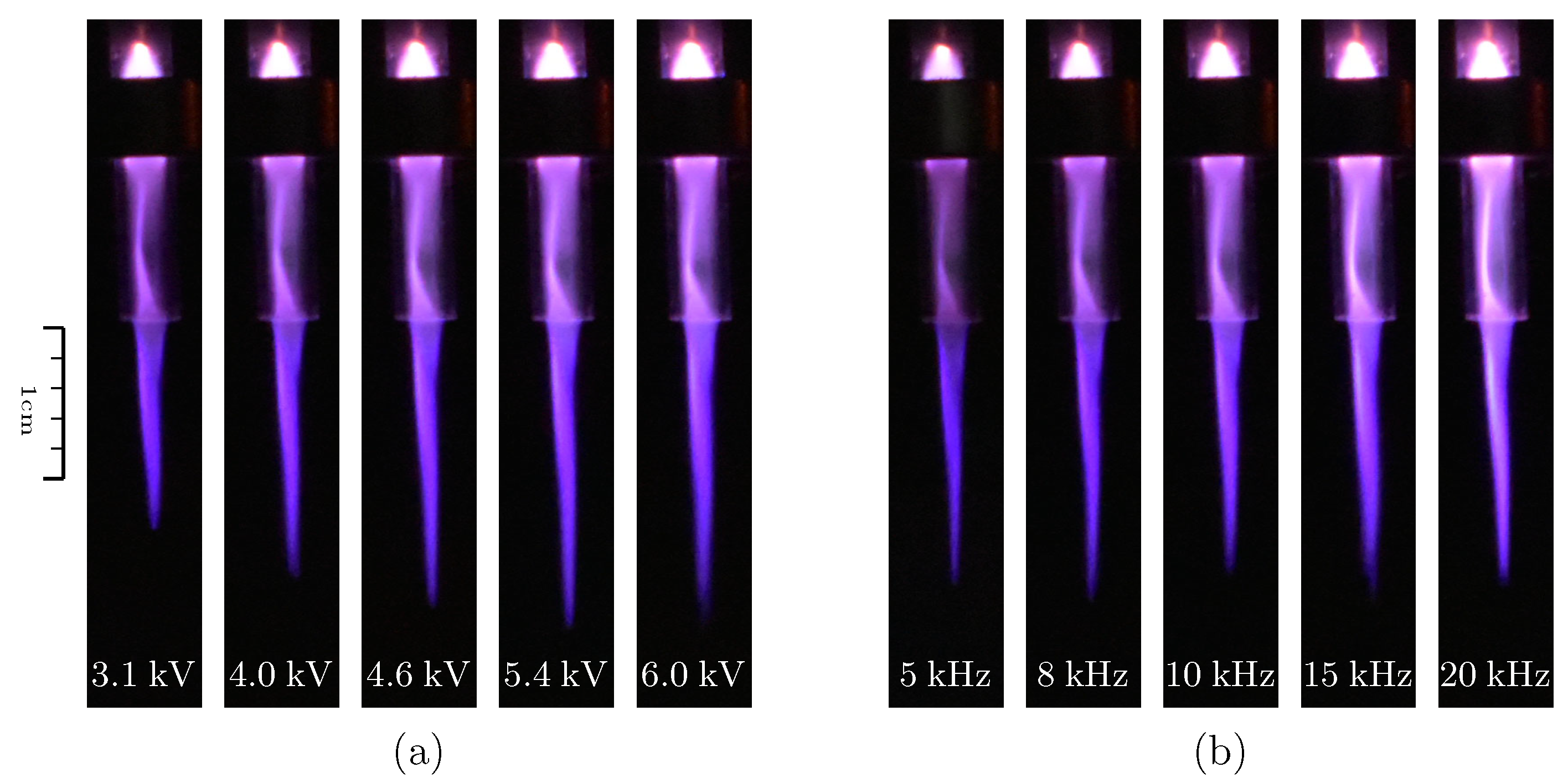
Using the uni-polar pulses, the helium plasma jet in the system of Figure 2 can be obtained. In the experiments, the pulse width of high voltage T W is maintained at 10 μs, and the flow rate of helium is fixed at 1400 sccm. Figure 9 presents the time-integrated images of the plasma jet recorded by the CCD camera. The exposure time of all images is 0.5 s.
Figure 9a shows the results at different voltage amplitudes with f = 10 kHz. The images show that the length of the helium plasma jet is influenced by V amp significantly. At V amp = 3.1 kV, the length of the jet is about 12 mm and increases to ∼20 mm at V amp = 5.4 kV. However, when further increasing V amp , the jet length tends to become saturated or even decrease.
The jet length is affected by pulse frequency slightly. At V amp = 4 kV, when the pulse frequency increases from 5 kHz to 20 kHz, the jet length changes only about 1 mm, as shown in Figure 9b. While the brightness of the plasma jet increases with f significantly. The effects of voltage and frequency on the plasma jet are similar to that in Ref. [38].

4.2. Discharge Current

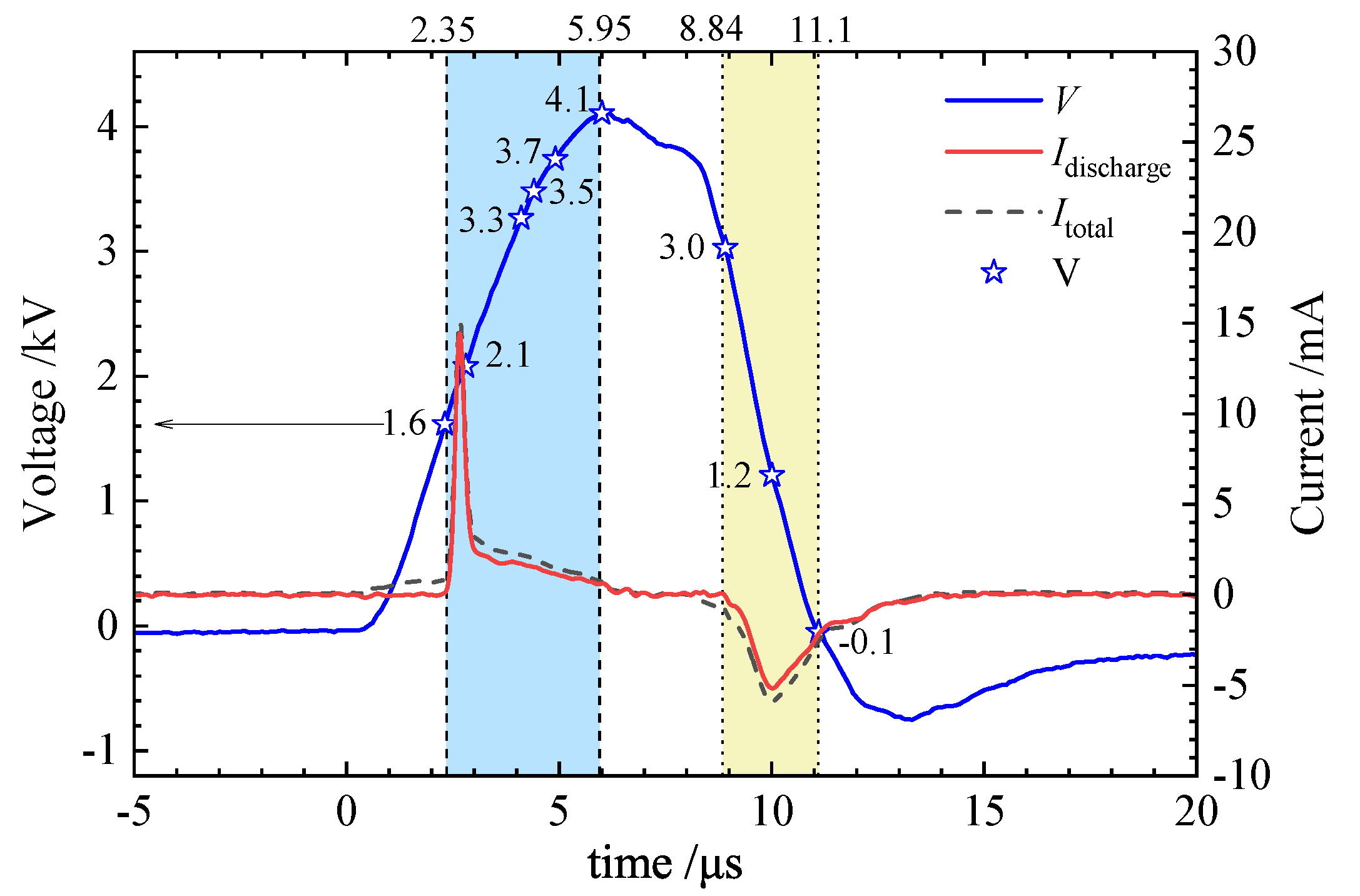
The generation of helium plasma jet depends on the discharge process. Figure 10 provides two typical discharge current waveforms and a corresponding voltage waveform on the needle electrode with f = 10 kHz and T W = 10  μs. The gray dashed curve is the total current I total measured on the grounded electrode, and the red solid curve is the discharge current I discharge obtained by subtracting the displacement current from I total . As can be seen from Figure 10, the waveform of the discharge current I discharge almost coincides with that of the total current I total . At the rising and falling edges, the voltage of the microsecond pulse changes much more slowly than the nanosecond pulse; therefore, the displacement current is very small and can be ignored.
The current in Figure 10 shows that driven by the microsecond uni-polar pulse, a positive current pulse and a negative pulse are observed at the rising and falling edges of the voltage waveform, respectively, just as in many studies of nanosecond or microsecond pulse DBDs. The durations of the two current pulses are about 4∼6 μs. It can be found that the current increases rapidly at a voltage of 1.6 kV, which means that the discharge is ignited. The positive current pulse reaches a peak value of 18 mA as the voltage increases to ∼2.8 kV. Then, the current decreases to 3 mA within 1 μs, and the state of small current is maintained for about 4 μs. During the falling edge, reverse discharge is ignited, and a negative current pulse begins to occur when the voltage drops to 3 kV. This is caused by the charges accumulated on the quartz tube wall. The negative current peak is only about 6.6 mA. Both positive and negative peaks of discharge current are much lower than that in nanosecond pulsed plasma jets [20,24,25], which reduces the electromagnetic interference of the discharge significantly.

4.3. Propagation of the Plasma Jet

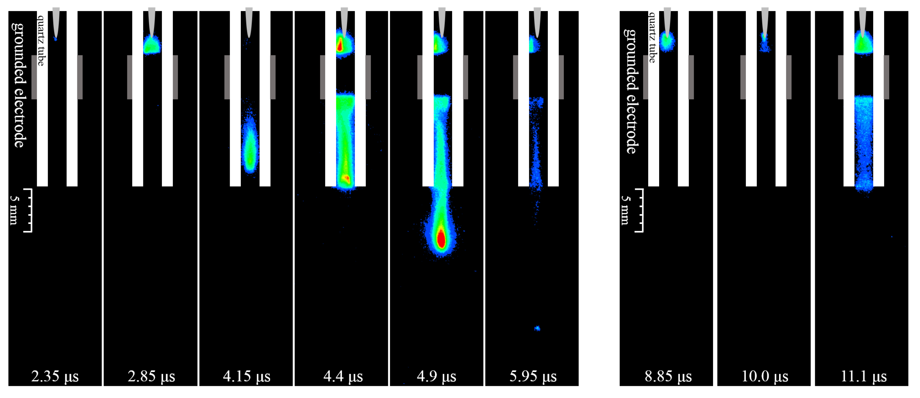
Figure 11 presents the ICCD time-resolved images of the light emission by the discharge and jet plasma with the high-voltage pulse in Figure 10. The number of accumulations of ICCD is 1, which means that each image is obtained by a single shot. The gate width and the gate step of ICCD are both 50 ns. All images are drawn with the same levels of intensity. The time of each image is marked with an asterisk within the two shaded areas of Figure 10. From Figure 11a, it can be seen that at about 2.35 μs, the discharge during rising edge is ignited at the needle tip. At this moment, the voltage on needle is 1.6 kV, as shown in Figure 10. Then the discharge develops from the needle electrode towards the ground electrode quickly, and a bright plasma channel is built between the needle and the grounded electrode at 2.85 μs. The discharge at this stage forms the peak of the positive current pulse in Figure 10. After that, the plasma channel between the power electrode and grounded electrode begins to decay, while the plasma moves towards the outlet of quartz tube gradually, as shown by the image of 4.15 μs in Figure 11a.
At 4.4 μs, the light emission in the whole region between the needle and the tube outlet is observed. The intensity also becomes stronger. It is considered that the voltage on the needle is increased to 3.5 kV, which enhances the discharge. Thereafter, the plasma jet is formed and propagates outside the tube. During the phase, both the luminescence and size of plasma bullet increase significantly (see image of 4.9 μs). Then, the plasma bullet attenuates gradually with propagating.
The time-resolved images of the plasma during the falling edge of the high-voltage pulse are presented in Figure 11b. The results show that no plasma jet is observed outside the quartz tube. There is only a weak discharge between the needle and the ground electrode. The strongest radiation appears at the tip of the power electrode, which is consistent with negative corona discharge. The discharge at this stage is caused by the electric field of the charges accumulated on the inner wall of the quartz tube. Due to the decrease of applied voltage and the elimination of wall charges, the electric field is always weak, so a strong discharge and plasma jets cannot be generated. The jets are only formed during the rising edge of the pulsed voltage, which makes the jet propagation at different frequencies (under the same pulsed voltage) more consistent. Therefore, the jet length changes slightly as the frequency increases.

4.4. Spectra of the Jet

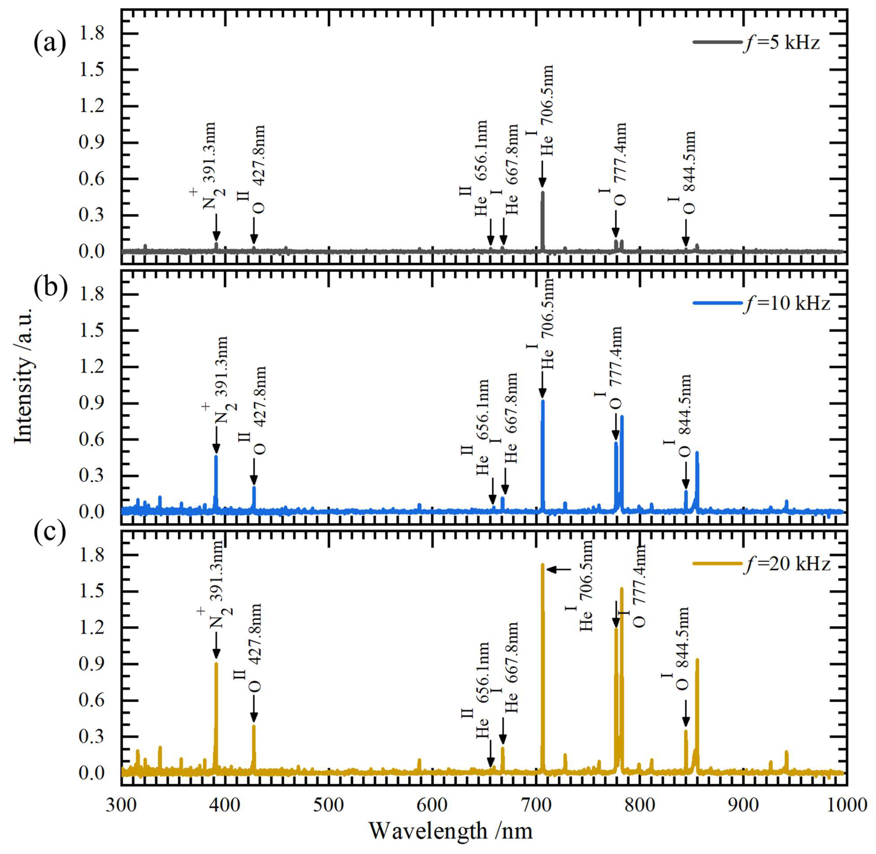
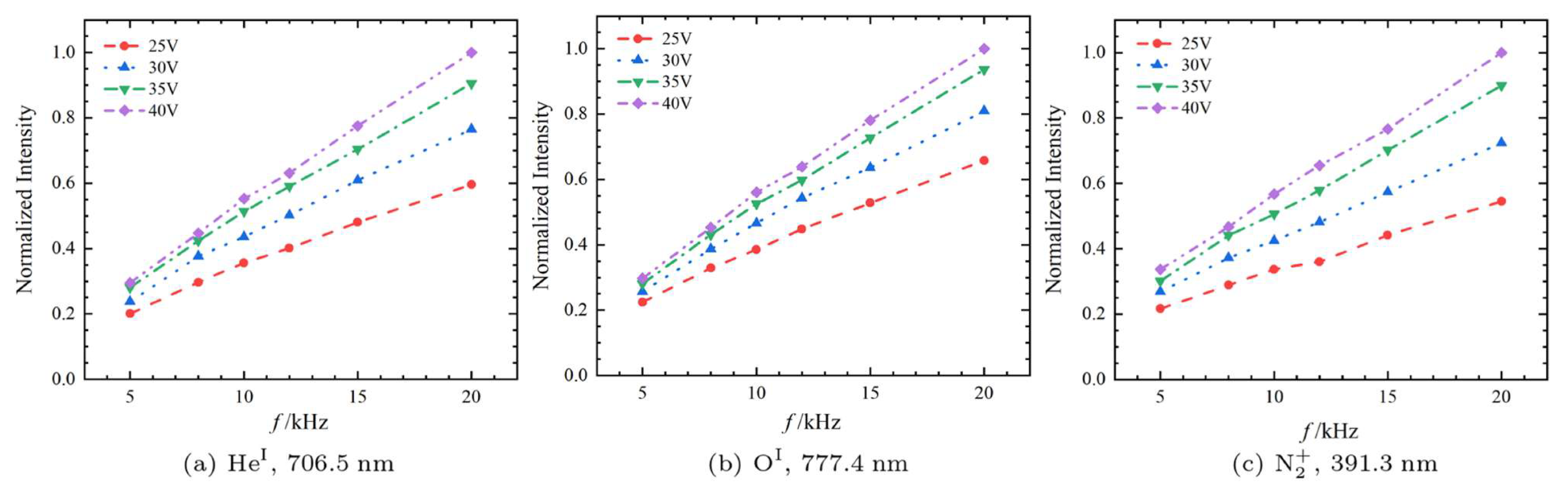
Figure 12 shows the emission spectra of plasma jet at different frequencies. The integration time is 3 s to cover several discharge pulses. The pulse widths T W and V amp are fixed at 10 μs and 4 kV, respectively. As with the results in many helium plasma jets, the emission spectra measured in our experiment mainly include the spectral lines of helium (HeI 706.5 nm, HeI 667.8 nm), oxygen (OI 777.4 nm, OI 844.5 nm), and nitrogen ( N 2 + 391.3 nm). The normalized intensities of the selected emission lines are further summarized in Figure 13. The results show that the intensities of HeI 706.5 nm, OI 777.4 nm, and N 2 + 391.3 nm exhibit approximately linear increasing trends with pulse frequency in the voltage range of this work. Thus, although the generation of reactive species in the plasma jet depends on more complex processes, it is still expected that the number of species can be controlled by changing the frequency of the pulsed source.

5. Conclusions

In this paper, a low-cost, compact microsecond pulsed power source is designed. The pulsed supply can be powered by a 12 V low-voltage DC unit. And the maximum bus voltage supplied to the half-bridge circuit is 36 V, which can use low-voltage and low-price devices in the power supply. Uni-polar and bi-polar quasi-square high-voltage pulses can be generated by this pulsed source. The amplitude of high-voltage pulse can be adjusted by DC voltage linearly from 0 to 5 kV with frequency up to 20 kHz. The minimum of the pulse width is ∼10 μs with rising and falling edges around 3∼5 μs. The uni-polar pulse was used to drive a helium plasma jet with needle-ring configuration. At both rising and falling edges of the pulsed voltage, a single pulse of the discharge current is obtained. The propagation of plasma bullets outside the quartz tube was observed only at the rising edge of the voltage pulse, which makes the jet development at different frequencies (with the same pulsed voltage) more consistent. Therefore, the length of the plasma jet is almost unaffected by the frequency. The normalized intensities of the emission lines increase linearly with pulse frequency.

Author Contributions

Conceptualization, C.M. and F.H.; methodology, C.M. and F.H.; investigation, C.M., L.Y. and J.L.; writing—original draft preparation, C.M.; writing—review and editing, F.H.; supervision, F.H.; and funding acquisition, F.H. All authors have read and agreed to the published version of the manuscript.

Funding

This work was supported by the National Science Foundation of China under Grant No. 11475019.

Institutional Review Board Statement

Not applicable.

Informed Consent Statement

Not applicable.

Data Availability Statement

The data presented in this study are available in the article.

Conflicts of Interest

The authors declare no conflicts of interest.

Abbreviations

The following abbreviations are used in this manuscript:
APPJAtmospheric pressure plasma jet
DBDDielectric barrier discharge
DCDirect current
ICCDIntensified charge-coupled device
OESOptical emission spectra
PWMPulse-width modulation
RFRadio frequency

References

  1. Winter, J.; Brandenburg, R.; Weltmann, K.-D. Atmospheric pressure plasma jets: An overview of devices and new directions. Plasma Sources Sci. Technol. 2015, 24, 064001. [Google Scholar] [CrossRef] [Scilit]
  2. Kumar, N.; Attri, P.; Choi, E.H.; Uhm, H.S. Influence of water vapour with non-thermal plasma jet on the apoptosis of SK-BR-3 breast cancer cells. RSC Adv. 2015, 5, 14670–14677. [Google Scholar] [CrossRef] [Scilit]
  3. Viegas, P.; Slikboer, E.; Bonaventura, Z.; Guaitella, O.; Sobota, A.; Bourdon, A. Physics of plasma jets and interaction with surfaces: Review on modelling and experiments. Plasma Sources Sci. Technol. 2022, 31, 053001. [Google Scholar] [CrossRef] [Scilit]
  4. Shang, H.; Ning, W.; Shen, S.; Wang, R.; Dai, D.; Jia, S. Atmospheric pressure plasma jet for surface treatment: A review. Rev. Mod. Plasma Phys. 2025, 9, 3. [Google Scholar] [CrossRef] [Scilit]
  5. Xu, C.-H.; Shen, P.-Y.; Chiu, Y.-F.; Yeh, P.-W.; Chen, C.-C.; Chen, L.-C.; Hsu, C.-C.; Cheng, I.-C.; Chen, J.-Z. Atmospheric pressure plasma jet processed nanoporous Fe2O3/CNT composites for supercapacitor application. J. Alloys Compd. 2016, 676, 469–473. [Google Scholar] [CrossRef] [Scilit]
  6. Toshifuji, J.; Katsumata, T.; Takikawa, H.; Sakakibara, T.; Shimizu, I. Cold arc-plasma jet under atmospheric pressure for surface modification. Surf. Coat. Technol. 2003, 171, 302–306. [Google Scholar] [CrossRef] [Scilit]
  7. Stoffels, E.; Kieft, I.E.; Sladek, R.E.J. Superficial treatment of mammalian cells using plasma needle. J. Phys. D Appl. Phys. 2003, 36, 2908–2913. [Google Scholar] [CrossRef] [Scilit]
  8. Lu, X.; Jiang, Z.; Xiong, Q.; Tang, Z.; Pan, Y. A single electrode room-temperature plasma jet device for biomedical applications. Appl. Phys. Lett. 2008, 92, 151504. [Google Scholar] [CrossRef] [Scilit]
  9. Laroussi, M.; Lu, X. Room-temperature atmospheric pressure plasma plume for biomedical applications. Appl. Phys. Lett. 2005, 87, 113902. [Google Scholar] [CrossRef] [Scilit]
  10. Pei, X.; Kredl, J.; Lu, X.; Kolb, J.F. Discharge modes of atmospheric pressure DC plasma jets operated with air or nitrogen. J. Phys. D Appl. Phys. 2018, 51, 384001. [Google Scholar] [CrossRef] [Scilit]
  11. Schweigert, I.V.; Alexandrov, A.L.; Zakrevsky, D.E. Self-organization of touching-target current with ac voltage in atmospheric pressure plasma jet for medical application parameters. Plasma Sources Sci. Technol. 2020, 29, 12LT02. [Google Scholar] [CrossRef] [Scilit]
  12. Gazeli, K.; Svarnas, P.; Lazarou, C.; Anastassiou, C.; Georghiou, G.E.; Papadopoulos, P.K.; Clément, F. Physical interpretation of a pulsed atmospheric pressure plasma jet following parametric study of the UV-to-NIR emission. Phys. Plasmas 2020, 27, 123503. [Google Scholar] [CrossRef] [Scilit]
  13. Reuter, S.; von Woedtke, T.; Weltmann, K.-D. The kINPen—A review on physics and chemistry of the atmospheric pressure plasma jet and its applications. J. Phys. D Appl. Phys. 2018, 51, 233001. [Google Scholar] [CrossRef] [Scilit]
  14. Rath, S.; Kar, S. Microwave atmospheric pressure plasma jet: A review. Contrib. Plasma Phys. 2025, 65, e202400036. [Google Scholar] [CrossRef] [Scilit]
  15. Jiang, C.; Sözer, E.B.; Song, S.; Lai, N.; Vernier, P.T.; Guo, S. Modulation of ROS in nanosecond-pulsed plasma-activated media for dosage-dependent cancer cell inactivation in vitro. Phys. Plasmas 2020, 27, 113513. [Google Scholar] [CrossRef] [Scilit]
  16. Li, S.-Z.; Xu, M.-C.; Zhang, X.; Zhang, J.-L. A pulse-modulated nonequilibrium atmospheric-pressure microwave argon plasma discharge preionized by a kilohertz excited plasma jet. Appl. Phys. Lett. 2012, 100, 174101. [Google Scholar] [CrossRef] [Scilit]
  17. Uchida, G.; Takenaka, K.; Setsuhara, Y. Effects of discharge voltage waveform on the discharge characteristics in a helium atmospheric plasma jet. J. Appl. Phys. 2015, 117, 153301. [Google Scholar] [CrossRef] [Scilit]
  18. Pinchuk, M.E.; Stepanova, O.M.; Gromov, M.; Leys, C.; Nikiforov, A. Variation in guided streamer propagation along a DBD plasma jet by tailoring the applied voltage waveform. Appl. Phys. Lett. 2020, 116, 164102. [Google Scholar] [CrossRef] [Scilit]
  19. Huang, B.; Zhang, C.; Sun, H.; Sorokin, D.A.; Tarasenko, V.F.; Shao, T. Enhancement of hydrogen radical density in atmospheric pressure plasma jet by a burst of nanosecond pulses at 1 MHz. Plasma Sources Sci. Technol. 2022, 31, 025019. [Google Scholar] [CrossRef] [Scilit]
  20. Shen, S.; Yan, J.; Wang, Y.; Wang, Y.; Ding, W.; Sun, G. Stepwise development of atmospheric pressure plasma jet driven by bursts of high-voltage nanosecond pulses at multi-tens MHz. Plasma Sources Sci. Technol. 2022, 31, 105003. [Google Scholar] [CrossRef] [Scilit]
  21. Ivankov, A.; Capela, T.; Rueda, V.; Bru, E.; Piquet, H.; Schitz, D.; Florez, D.; Diez, R. Experimental study of a nonthermal DBD-driven plasma jet system using different supply methods. Plasma 2022, 5, 75–97. [Google Scholar] [CrossRef] [Scilit]
  22. Patelli, A.; Scaltriti, S.G.; Popoli, A.; Martines, E.; Cristofolini, A. Plasma-substrate interaction in a dual frequency APPJ. Plasma Sources Sci. Technol. 2025, 34, 025010. [Google Scholar] [CrossRef] [Scilit]
  23. Wang, L.; Liu, C.; Wu, J.; Hu, X.; Chen, S.; Cheng, T.; Lu, H.; Chen, Z. Discharge characteristics of an atmospheric pulsed microwave Ar/CF4 plasma jet. AIP Adv. 2023, 13, 095023. [Google Scholar] [CrossRef] [Scilit]
  24. Lu, X.; Laroussi, M. Dynamics of an atmospheric pressure plasma plume generated by submicrosecond voltage pulses. J. Appl. Phys. 2006, 100, 063302. [Google Scholar] [CrossRef] [Scilit]
  25. Walsh, J.L.; Kong, M.G. Room-temperature atmospheric argon plasma jet sustained with submicrosecond high-voltage pulses. Appl. Phys. Lett. 2007, 91, 221502. [Google Scholar] [CrossRef] [Scilit]
  26. Walsh, J.L.; Kong, M.G. Portable nanosecond pulsed air plasma jet. Appl. Phys. Lett. 2011, 99, 081501. [Google Scholar] [CrossRef] [Scilit]
  27. Jiang, C.; Chen, M.T.; Gundersen, M.A. Polarity-induced asymmetric effects of nanosecond pulsed plasma jets. J. Phys. D Appl. Phys. 2009, 42, 232002. [Google Scholar] [CrossRef] [Scilit]
  28. Robert, E.; Barbosa, E.; Dozias, S.; Vandamme, M.; Cachoncinlle, C.; Viladrosa, R.; Pouvesle, J.M. Experimental study of a compact nanosecond plasma gun. Plasma Process. Polym. 2009, 6, 795–802. [Google Scholar] [CrossRef] [Scilit]
  29. Liu, Z.; Wang, S.; Pang, B.; Gao, Y.; Li, Q.; Xu, D.; Liu, D.; Zhou, R. A novel designed 3D multi-microhole plasma jet device driven by nanosecond pulse at atmospheric pressure. Plasma Sources Sci. Technol. 2022, 31, 05LT03. [Google Scholar] [CrossRef] [Scilit]
  30. Douat, C.; Kacem, I.; Sadeghi, N.; Bauville, G.; Fleury, M.; Puech, V. Space-time resolved density of helium metastable atoms in a nanosecond pulsed plasma jet: Influence of high voltage and pulse frequency. J. Phys. D Appl. Phys. 2016, 49, 285204. [Google Scholar] [CrossRef] [Scilit]
  31. Huang, B.; Zhang, C.; Zhu, W.; Lu, X.; Shao, T. Ionization waves in nanosecond pulsed atmospheric pressure plasma jets in argon. High Volt. 2021, 6, 665–673. [Google Scholar] [CrossRef] [Scilit]
  32. Zhao, S.; van de Wege, R.; Sobota, A. Nitric oxide (NO) production in a kHz pulsed Ar plasma jet operated in ambient air. Plasma Sources Sci. Technol. 2025, 34, 045013. [Google Scholar] [CrossRef] [Scilit]
  33. Hamdan, A.; Zamo, A. Interaction of an open-to-air helium plasma jet, produced by sub-microsecond discharges, with a polystyrene surface. Plasma Process. Polym. 2025, 22, 2400220. [Google Scholar] [CrossRef] [Scilit]
  34. Malik, M.A.; Schoenbach, K.H.; Abdel-Fattah, T.M.; Heller, R.; Jiang, C. Low cost compact nanosecond pulsed plasma system for environmental and biomedical applications. Plasma Chem. Plasma Process. 2017, 37, 59–76. [Google Scholar] [CrossRef] [Scilit]
  35. Shen, S.; Tampieri, F.; Garcia, M.C.; Canal, C. Design and characterization of a nano-pulsed atmospheric pressure plasma jet for biomedical applications. Plasma Process. Polym. 2024, 21, e2400086. [Google Scholar] [CrossRef] [Scilit]
  36. Zhang, C.; Shao, T.; Wang, R.; Zhou, Z.; Zhou, Y.; Yan, P. A comparison between characteristics of atmospheric-pressure plasma jets sustained by nanosecond- and microsecond-pulse generators in helium. Phys. Plasmas 2014, 21, 103505. [Google Scholar] [CrossRef] [Scilit]
  37. Mashayekh, S.; Cvetanović, N.; Sretenović, G.B.; Obradović, B.M.; Liu, Z.; Yan, K.; Kuraica, M.M. Experimental study of a microsecond-pulsed cold plasma jet. Eur. Phys. J. D 2023, 77, 115. [Google Scholar] [CrossRef] [Scilit]
  38. Zhang, C.; Shao, T.; Wang, R.; Huang, W.; Niu, Z.; Schamiloglu, E. A repetitive microsecond pulse generator for atmospheric pressure plasma jets. IEEE Trans. Dielectr. Electr. Insul. 2015, 22, 1907–1915. [Google Scholar] [CrossRef] [Scilit]
  39. Fang, Z.; Shi, Y.; Liu, F.; Zhou, R. Compact microsecond pulsed power generator driven by solar energy for dielectric barrier discharge applications. IEEE Trans. Dielectr. Electr. Insul. 2019, 26, 390–396. [Google Scholar] [CrossRef] [Scilit]
  40. Jia, F.; Wu, Y.; Min, Q.; Su, M.; Takeda, K.; Ishikawa, K.; Kondo, H.; Sekine, M.; Hori, M.; Zhong, Z. Characterization of a microsecond pulsed non-equilibrium atmospheric pressure Ar plasma using laser scattering and optical emission spectroscopy. Plasma Sci. Technol. 2020, 22, 065404. [Google Scholar] [CrossRef] [Scilit]
  41. Jin, S.; Chen, J.; Li, Z.; Zhang, C.; Zhao, Y.; Fang, Z. Novel RDD pulse shaping method for high-power high-voltage pulse current power supply in DBD application. IEEE Trans. Ind. Electron. 2022, 69, 12653–12664. [Google Scholar] [CrossRef] [Scilit]
  42. Jin, S.; Wang, S.; Zhao, K.; Jiang, Y.; Zhao, S.; Zhao, Y.; Fang, Z. A high-drive-performance microsecond pulse power module for portable DBD plasma source device. IEEE Trans. Power Electron. 2023, 38, 15072–15085. [Google Scholar] [CrossRef] [Scilit]
Figure 1. Schematic diagram (a) and photograph (b) of the microsecond pulsed power supply. (c) Geometry diagram of toroidal ferrite core used for P T 1 .
Plasma 09 00019 g001
Figure 2. Schematic of the APPJ experimental setup. The arrows indicate the helium flow direction and the measurement connections.
Plasma 09 00019 g002
Figure 3. Simulation of the μs pulse source. (a) The circuit model. (b) Voltage waveforms of the primary and secondary coils by simulation.
Plasma 09 00019 g003
Figure 4. Typical output waveforms of the μs pulsed power supply. (a) Uni-polar pulses. (b) Bi-polar pulses.
Plasma 09 00019 g004
Figure 5. Voltage waveforms of uni-polar pulse at different frequencies. V bus = 30 V.
Plasma 09 00019 g005
Figure 6. Voltage waveform and voltage amplitude V amp at different V bus . f = 10 kHz.
Plasma 09 00019 g006
Figure 7. Averaged power P avg versus the voltage V bus and frequency f.
Plasma 09 00019 g007
Figure 8. QV Lissajous curve of the APPJ. V bus = 30 V, f = 10 kHz, and T W = 10  μs. Gas flow rate is 1400 sccm.
Plasma 09 00019 g008
Figure 9. Time integrated images of the plasma jet driven by uni-polar pulse. T W = 10  μs. (a) At different V amp . f = 10 kHz. (b) At different frequencies. V amp = 4 kV.
Plasma 09 00019 g009
Figure 10. Voltage and current waveforms of the discharge during a uni-polar pulse. f = 10 kHz, T W = 10  μs.
Plasma 09 00019 g010
Figure 11. Time-resolved images of the helium plasma jet with μs voltage pulse. f = 10 kHz, T w = 10  μs.
Plasma 09 00019 g011
Figure 12. Representative two-dimensional emission spectra of the plasma jet at different pulse frequencies. (a) f = 5 kHz. (b) f = 10 kHz. (c) f = 20 kHz. T W = 10  μs, V amp = 4 kV.
Plasma 09 00019 g012
Figure 13. Normalized intensities of emission lines as functions of pulse frequency and V amp .
Plasma 09 00019 g013
Disclaimer/Publisher’s Note: The statements, opinions and data contained in all publications are solely those of the individual author(s) and contributor(s) and not of MDPI and/or the editor(s). MDPI and/or the editor(s) disclaim responsibility for any injury to people or property resulting from any ideas, methods, instructions or products referred to in the content.