


Abstract
Solar cell efficiency depends on both photogeneration and charge collection, with the active layer playing a key role in these processes. In organic solar cells (OSCs), where power conversion efficiency (PCE) remains relatively low, understanding the influence of active layer and metal contact thickness on device performance is essential. In this work, we investigate the effect of P3HT:PCBM and Ag thickness on OSC performance by analyzing the evolution of electrical parameters obtained from J-V measurements over five weeks, with particular attention given to resistance-related degradation behavior. The analyzed OSCs had a cell structure composed of Ag/P3HT:PCBM/TiO2/ITO/glass, and each material was corroborated by XRD and Raman spectroscopy. The thickness of P3HT:PCBM was modulated by varying the number of spin-coated layers from 1 to 3 (ranging from 75 to 160 nm). This variation increases light absorption, as demonstrated by the optical transmittance spectra. However, device degradation became evident after the third week of fabrication, mainly due to an increase in series resistance, which adversely affected the open-circuit voltage (VOC), fill factor (FF), and overall device efficiency. The best performance was obtained for devices fabricated with two P3HT:PCBM layers and 18 mg of Ag, achieving a maximum PCE of 0.5%.
1. Introduction
Organic solar cells (OSCs) have attracted significant attention due to their potential for use in flexible and lightweight devices, as well as their suitability for large-scale roll-to-roll processing [1]. Among these types of devices, OSCs stand out due to their blend of poly(3-hexylthiophene) (P3HT) and the fullerene derivative [6,6]-phenyl-C61-butyric acid methyl ester (PCBM), serving as donor and acceptor materials, respectively. Two materials are blended to form the known bulk heterojunction (BHJ), which is implemented to increase the interfacial area and exciton dissociation [2]. This type of OSC consists of three fundamental layers in its most basic form: two electrodes, which are typically a transparent conductive oxide (TCO) and a metallic layer, and the P3HT:PCBM active layer situated between them. Under this configuration, P3HT:PCBM-based OSCs have achieved photoconversion efficiencies of around 5% [3,4], which are lower compared to those obtained with other technologies. Consequently, they are currently in the research stage. The primary disadvantages of organic semiconductors are attributed to their inherent properties, including short diffusion lengths, low mobility, and rapid charge-carrier recombination [5]. To address these limitations, different investigations have been conducted. The basic structure can be modified by incorporating electron and/or hole transporter layers (ETL and HTL, respectively) [6], examining various material configurations [7], doping the P3HT:PCBM active layer with inorganic nanoparticles [8], and investigating different materials, including electrodes and substrates [9,10], among others.
While the improvements from these changes are limited, in the long term, they will prove significant because the development of photovoltaic devices tends to progress slowly. However, achieving successful improvement requires a comprehensive understanding of the contribution of each component and its interaction within the device. Improving solar cell performance typically involves enhancing photogeneration and charge collection, which are regarded as the most crucial parameters. These are mainly related to the active layer and metal contact. In the first case, a thicker material absorbs more light. In the second case, it might be thought that the current collection rises as the metallic contact thickness increases. However, it is necessary to determine the point at which the thickness of the active layer or the metal contact can positively affect device performance.
The Current Density–Voltage (J-V) curve is the most common tool for evaluating the operation of photovoltaic devices. This method enables the acquisition of crucial electrical parameters, including the short-circuit current density (Jsc), open-circuit voltage (Voc), and fill factor (FF), which are used to calculate conversion efficiency (ƞ) [11]. The series resistance (Rs), one of the two types of resistors that make up the equivalent circuit of a solar cell, is another parameter that can be determined. The value is determined primarily by the bulk resistance of the active layer and the contact resistance in the electrodes. The Rs is a critical parameter for photovoltaic device performance, with its effects mainly reflected in the FF value and, consequently, in the photoconversion efficiency. Rs are less than 5 Ω·cm2 in solar cells based on inorganic materials such as CdTe and silicon, since higher values result in device degradation [12,13,14]. This is the reason why several authors have devoted considerable effort to elucidating the origin of Rs and its correlation with the properties of the layers that compose the device structure.
Given the substantial influence of series resistance (Rs) on the performance of photovoltaic devices, careful evaluation of its behavior is crucial for advancing the stability and photoconversion efficiency of organic solar cells (OSCs) [14,15]. In this context, systematic monitoring of device operation provides a valuable framework to elucidate the contribution of each component to overall performance. In this study, we investigate the effect of active layer thickness by tracking the evolution of electrical parameters in P3HT:PCBM-based OSCs over a five-week period. Weekly J–V measurements enabled the assessment of key parameters, including Voc, FF, Rs, and efficiency (η), thereby establishing correlations between active layer thickness and device stability. Notably, degradation was observed to initiate after the third week, underscoring the critical role of series resistance in long-term device performance. The aim of this work is to investigate thickness-dependent electrical evolution and stability trends in simplified OSC architectures, rather than achieving state-of-the-art device efficiency.
2. Results and Discussion
In this section, the effects of the active layer on the electrical properties of the OSCs are analyzed. The results were divided into two parts. In the first part, the properties of P3HT:PCBM with different thicknesses are studied. In the second part, the evolution of the electrical parameters of OSCs over time is analyzed. Hereafter, the nomenclature used for P3HT:PCBM samples will be 1L, 2L, and 3L for the active layers obtained with one, two, and three spin-coating depositions, respectively.
2.1. Active Layer Thickness
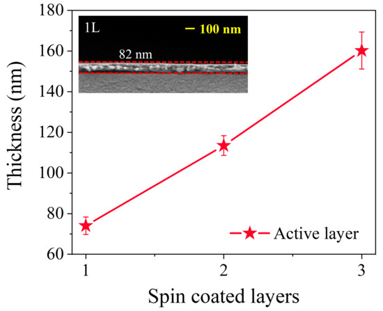
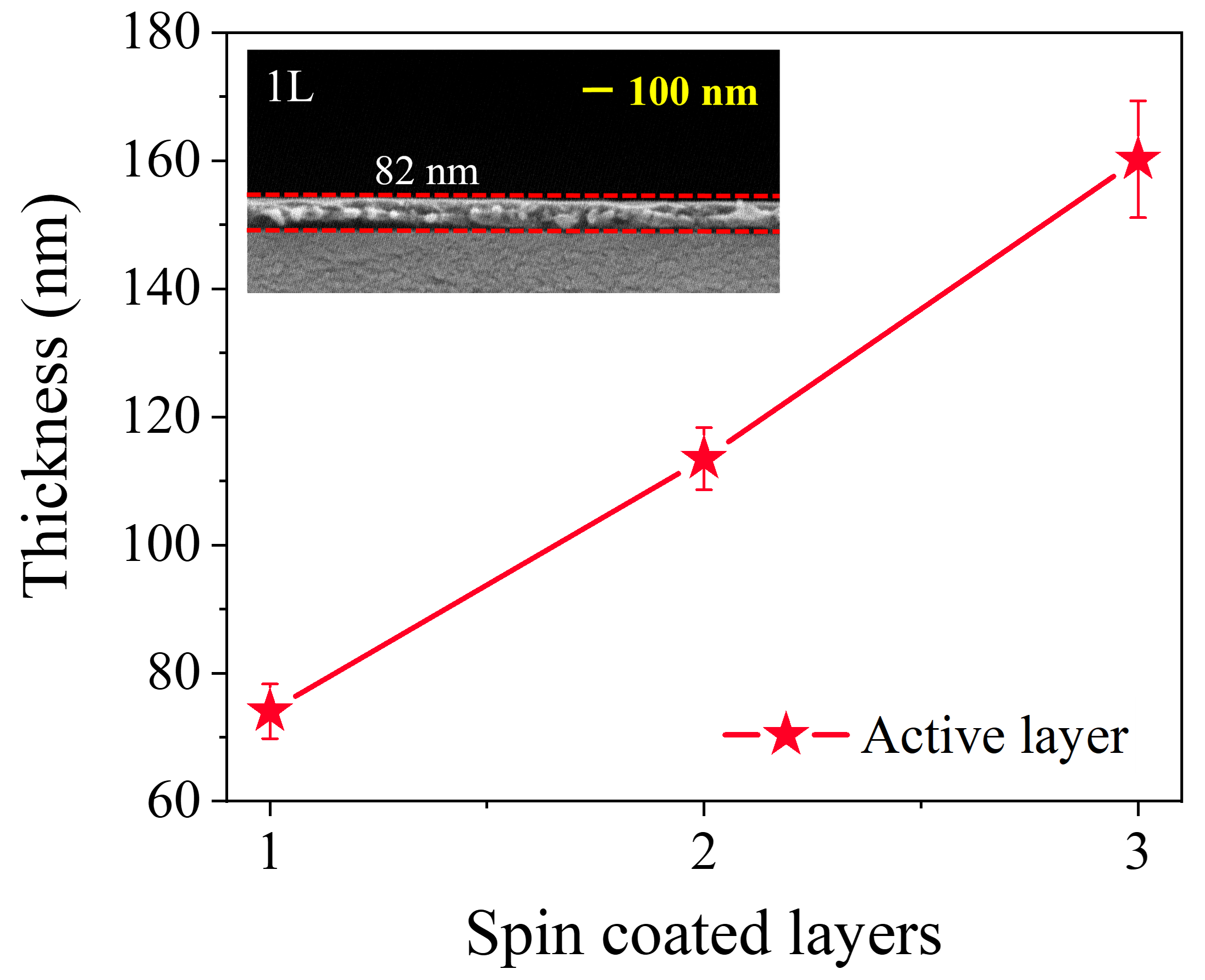
Figure 1 shows the thickness of P3HT:PCBM and Ag samples deposited onto glass substrates. It is worth noting that optical thickness measurements were performed at five points along the thin-film surface. Therefore, the reported values are an average of their respective error bars. As expected, the thickness of the active layer increases with an increasing number of spin-coated layers. The P3HT:PCBM thickness increased from 75 to 160 nm. In addition, cross-sectional FE-SEM images of the 1L sample corroborate the optical measurement of thickness, as shown in the inset of Figure 1.
Figure 1.
Thickness variation in P3HT:PCBM as a function of spin-coated layers.
2.2. Structural Properties
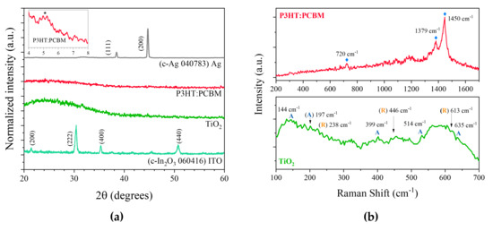
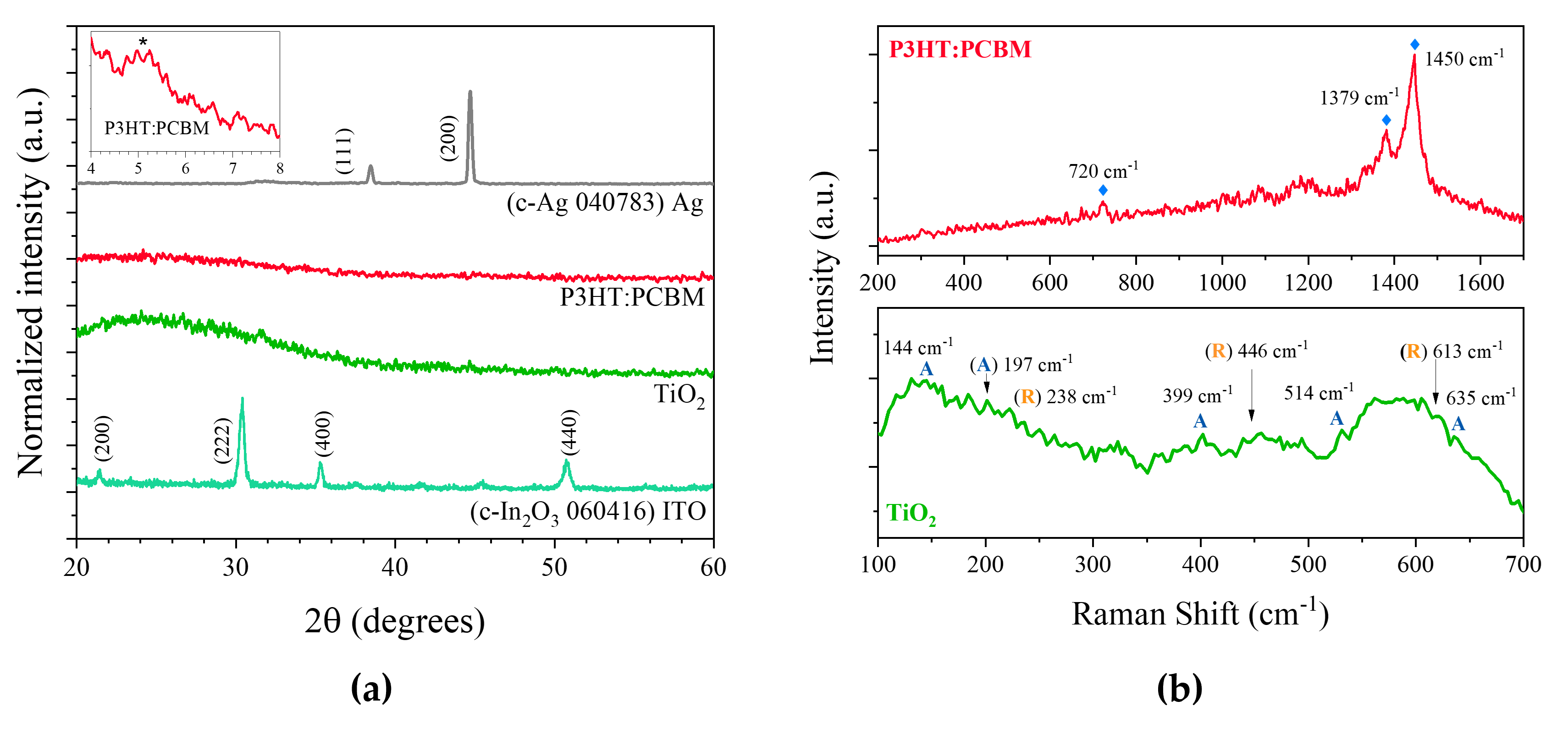
The fabricated organic solar cells are composed of four different materials, which are layered on top of each other and deposited by different deposition techniques. Therefore, it is essential to check their structural quality. Figure 2a shows the XRD patterns of each layer deposited on the glass substrates. Commercial ITO substrates possess a well-identified cubic structure according to JCPDS card number 06-0416. The XRD patterns display four peaks at 2Theta values of 21.4°, 30.4°, 35.3°, and 50.8°, corresponding to the (200), (222), (400), and (440) diffraction planes, respectively. In the case of the TiO2 thin film, no diffraction peaks are detected, revealing an amorphous film. In the P3HT:PCBM layer, no peaks were detected in the analyzed region. However, this organic material possesses a characteristic peak around 5° [16], as shown in the inset figure. The Ag metal contact shows a cubic crystalline structure (JCPDS card number 04-0783), with two intense and well-defined peaks at 38.4° and 44.7°, corresponding to the (111) and (200) planes, respectively.
Figure 2.
Structural properties of materials used for the OSC fabrication: (a) XRD patterns and (b) Raman spectra.
The Raman measurements of the TiO2 and P3HT:PCBM layers were performed to determine their structural nature. Figure 2b shows the corresponding spectra with a Raman shift range of 100 to 700 cm−1. TiO2 films exhibit vibrational modes that correspond to a mixture of anatase and rutile TiO2 phases. A possible cause of the absence of a crystallized film is the relatively low temperature used during the TiO2 deposition process [17,18]. In the case of the active layer, three distinct peaks are located at Raman shift 720, 1379, and 1450 cm−1, which are related to the P3HT:PCBM blend [19]. This section helps corroborate the presence of ITO, TiO2, the blended active layer, and Ag in the structure of the solar cell device.
2.3. Optical Properties
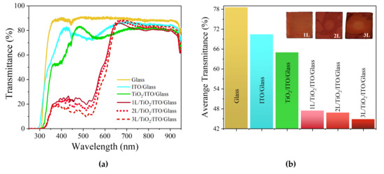
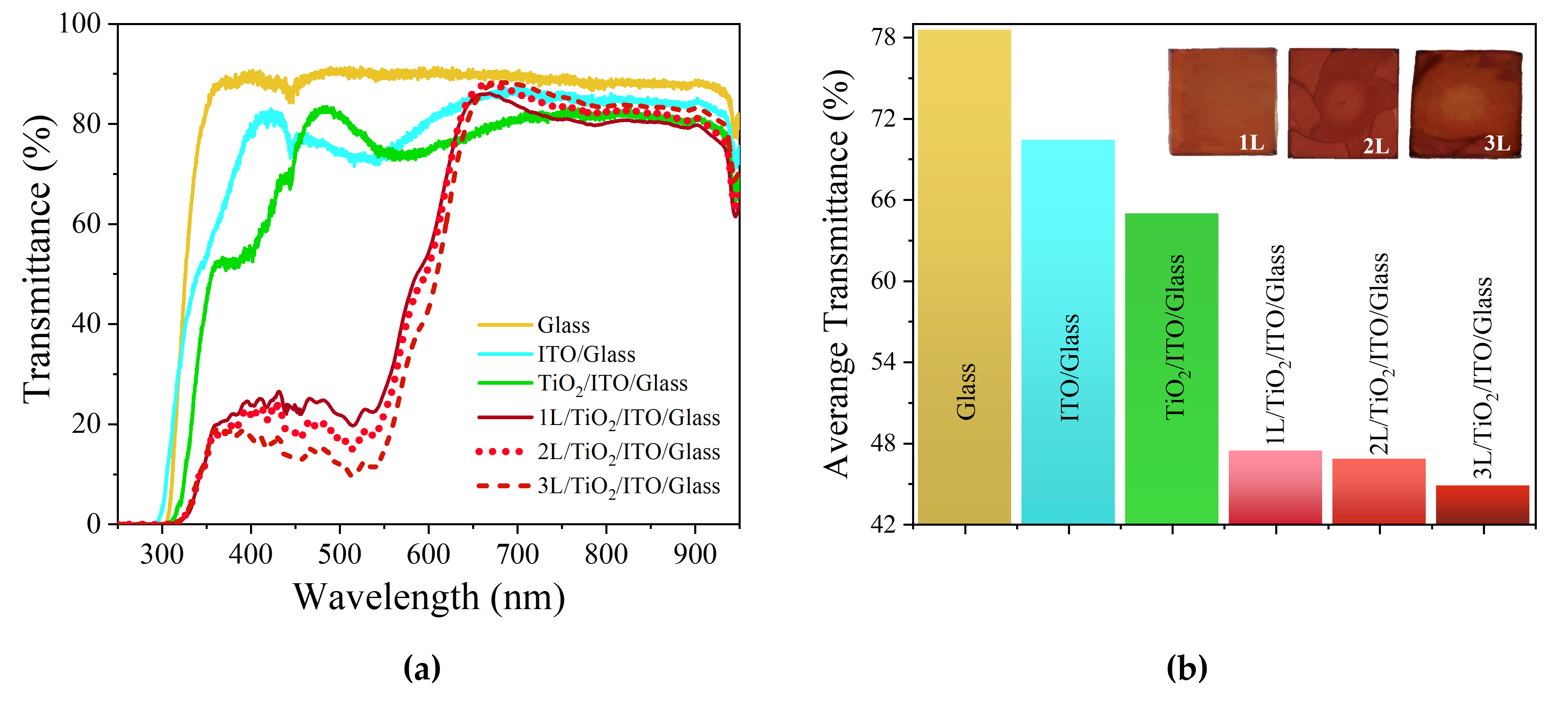
Ensuring effective light absorption by the active layer is a crucial factor during the fabrication of OSCs. In this context, the optical transmittance of each material in the device is a key factor. Therefore, the optical monitoring of the OSC structure during each manufacturing stage was carried out over the range 250–900 nm. Figure 3a exhibits the transmittance spectra of ITO/glass, TiO2/ITO/glass, and P3HT:PCBM/TiO2/ITO/glass. In addition, three different samples corresponding to the experimental conditions of 1L, 2L, and 3L are presented. As a new layer is incorporated into the OSC structure, the optical transmittance decreases, showing the minimum value with the addition of the active layer. This is corroborated by the average transmittance calculation, which was carried out in a range of 250–900 nm, as presented in Figure 3b. It is noteworthy that the commercial ITO substrate shows the highest value of approximately 70%, while the incorporation of the TiO2 layer reduces the average transmittance by six percentage points, exhibiting a value of around 64%.
Figure 3.
(a) Optical transmittance and (b) average transmittance of each material present in the device.
When an active layer is added, the structures with 1L, 2L, and 3L exhibit similar behavior, with two well-defined transmittance regions. The first one is located between 350 and 550 nm, and the second one is used for wavelengths higher than 650 nm, which are characteristic of P3HT and PCBM, respectively, since the active layer is a blend of both [20,21]. Furthermore, a notable variation is observed in the wavelength region between 450 and 600 nm, where a clear decrease in average transmittance is registered (from 47% to 44%) as the number of active layers increases from one to three. This increase in absorption and thickness is consistent with the findings reported by other researchers [22,23]. These variations are clearly visible in the inset images in Figure 3b, where samples appear red-purple and become progressively darker as the number of active layers increases. It is important to note that light absorption and photogeneration of charge carriers occur in the active layer; therefore, the increase in optical absorption could help to improve OSC performance.
2.4. Characterization of the Organic Solar Cell
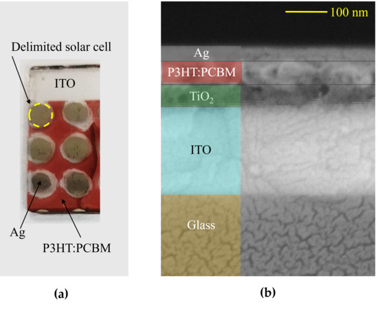
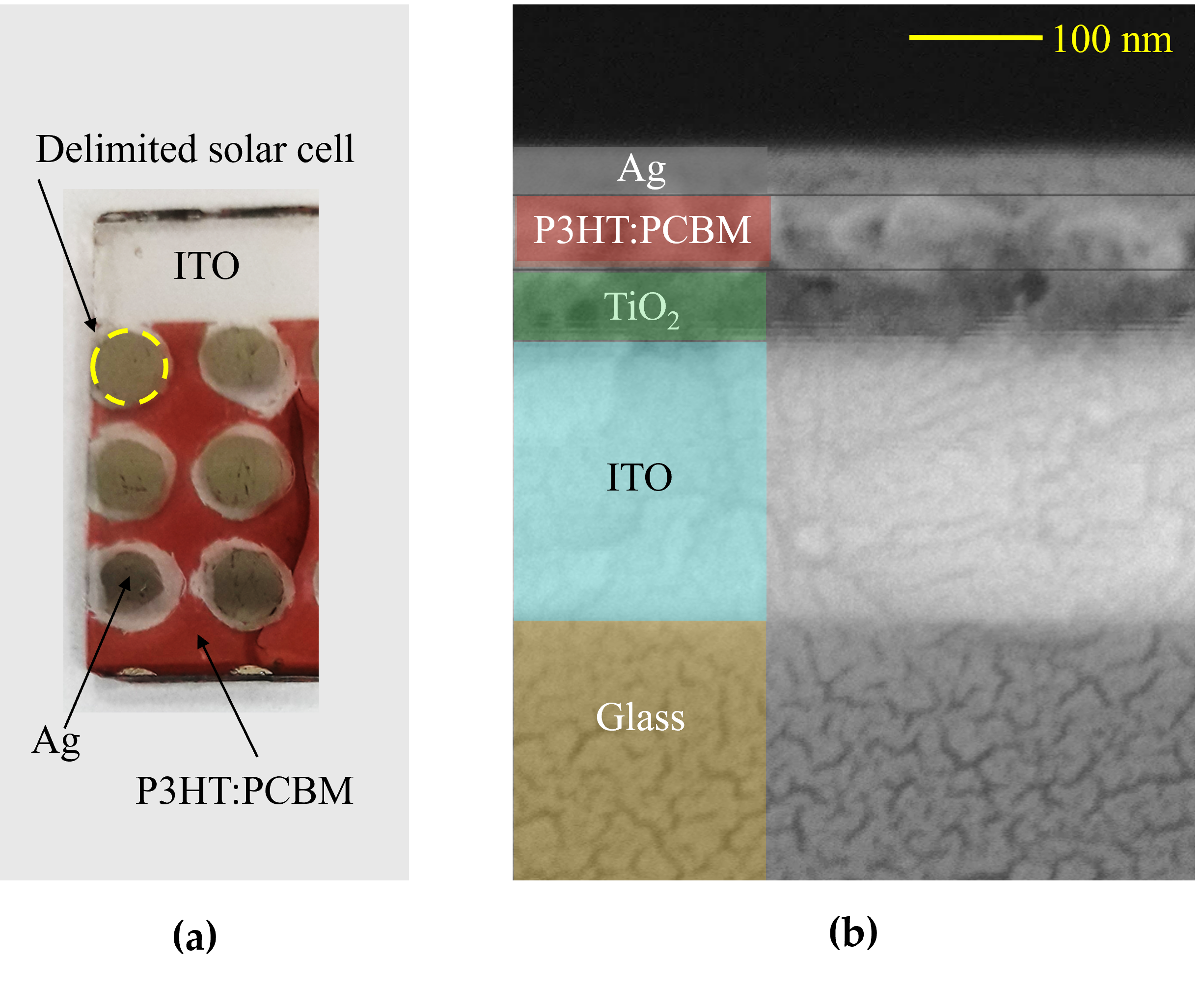
To analyze the thickness effect of P3HT:PCBM, Ag was evaporated on all cell structures (1L, 2L, and 3L), yielding six samples. Figure 4a shows a photographic image of the OSC fabricated and the nine individual cells obtained with the circular pattern mask used during the deposition of Ag metal contact. On the other hand, a cross-section SEM image of the Ag/P3HT:PCBM/TiO2/ITO/glass structure is presented in Figure 4b, where it is possible to observe each of the materials making up the device and the interfaces between them, which is necessary for understanding, improving, and developing the photovoltaic device.
Figure 4.
(a) Photograph and (b) cross-section image of the P3HT:PCBM solar cell.
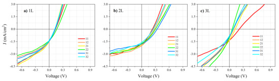
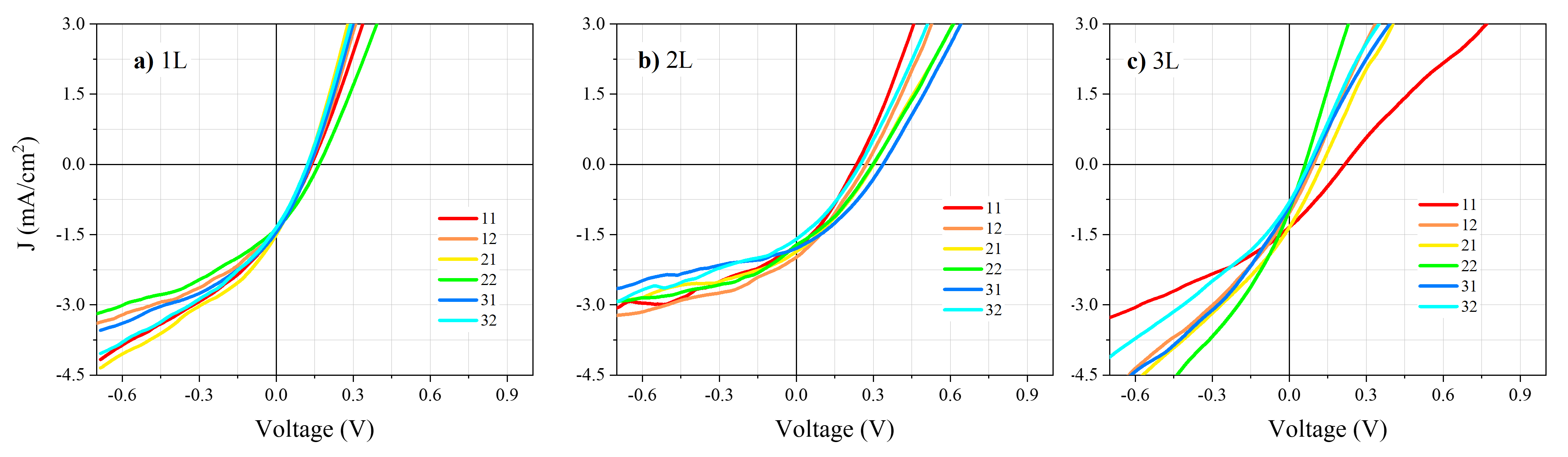
Figure 5 shows J-V curves representative of OSC structures with varying thickness of the active layers. It is important to note that the devices were measured on the same day that they were manufactured. Electrical parameters, including Jsc, Voc, and FF, were extracted from all solar cells in each sample, with average values summarized in Table 1. The efficiency (ƞ) was calculated using Equation (1), where Pin is the incident solar radiation:
Figure 5.
Representative J-V curves of P3HT:PCBM solar cells are shown as a function of the different active layer thicknesses.
Table 1.
Electrical parameters of the as-fabricated OSCs.
In general, the fabricated OSCs exhibit low electrical values: Jsc is around 1.5 mA/cm2, Voc is less than 300 mV, and FF is between 20 and 30%. This results in a photoconversion efficiency of around 0.1%. These results, although poor, are typical for these types of experimental/research devices given the properties of organic semiconductors [24]. However, the fabrication and study of OSCs are fundamental to understanding their behavior, the possible causes that generate it, and the relationship this holds with the variation in the thickness of the active layer. The most significant effects of increasing P3HT:PCBM thickness are mainly reflected in the values of Voc, which nearly doubles when the number of deposited layers is increased from one to two. In OSCs, the Voc has a linear relationship between the highest level of occupied molecular orbitals (HOMOs) of the donor material and the lowest level of unoccupied molecular orbitals (LUMOs) of the acceptor material [25]. Therefore, an improvement could indicate enhanced electronic and structural coupling between the acceptor and donor materials forming the P3HT:PCBM polymeric mixture. On the other hand, the Jsc exhibits a remarkable improvement, rising from 1.3 to 1.7 mA/cm2 as the thickness of P3HT:PCBM increases from 80 to 120 nm. This change could be directly linked to enhanced light absorption, as indicated by the optical transmittance spectra (Figure 3). If this trend continues, increasing the thickness of the active layer from two to three coatings would improve both Voc and Jsc. However, interestingly, an opposite behavior is observed: increasing the thickness of the active layer to 160 nm causes a decrease in electrical parameters and a distortion of the J-V curve, indicating a decay in the device’s performance. This reduction could be attributed to the intrinsic properties of organic semiconductors, such as their low mobility and short diffusion length, which limit the charge carriers’ mobility. Therefore, with a thicker active layer, the carriers are more difficult to collect at the electrical contacts of the device, increasing the probability of recombination and decreasing the current. Finally, according to some reports, an optimum active layer thickness of approximately 100 nm has been identified [14,26].
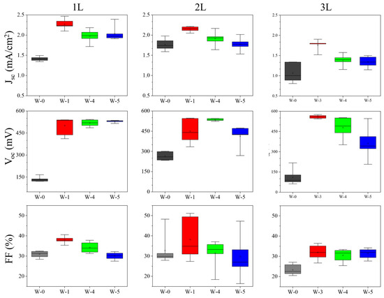
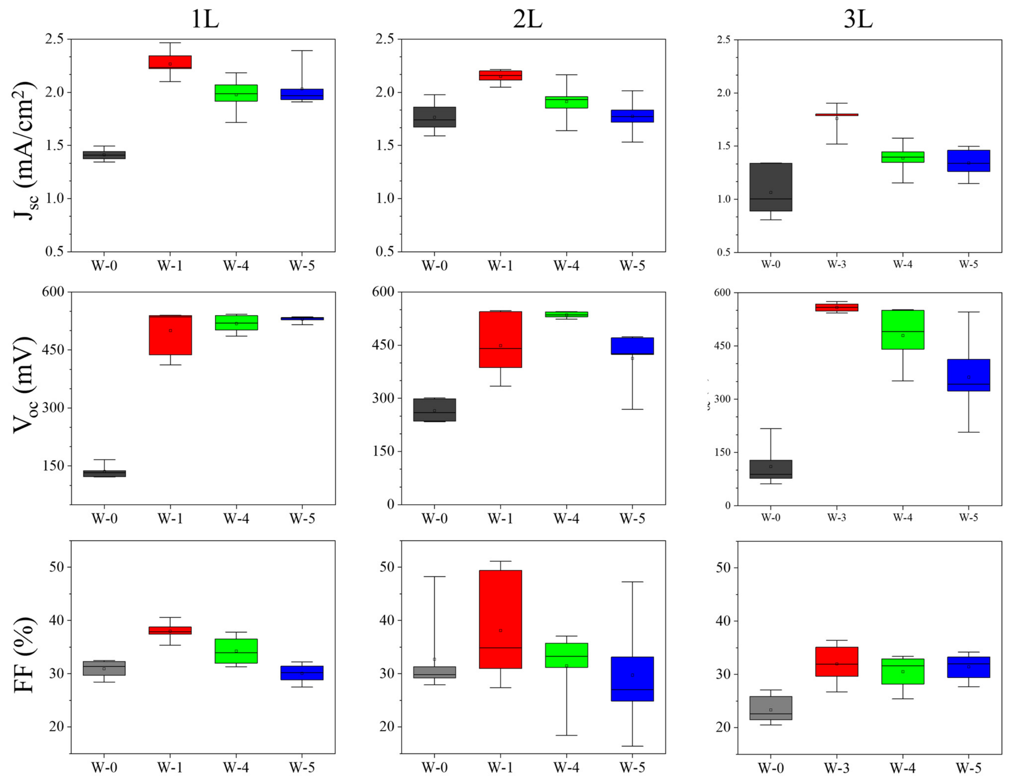
According to previous findings, the ideal thickness is approximately 120 nm, and this is achieved by applying two layers of P3HT:PCBM. However, as mentioned above, the results shown in Figure 5 correspond to the electrical characterization of the devices immediately after their manufacture. Here, low values may indicate the presence of defects within the cell structure, including irregular morphology, high carrier trapping, and improper interfacial layers. In the literature, it has been reported that a post-fabrication annealing process can improve electrical parameters by inducing a better molecular arrangement of the blend system and decreasing the defect states of the device [27,28]. Therefore, it is interesting to analyze their stability and evolution over time. The data presented in Figure 6 illustrates the progression of Jsc, Voc, and FF values over the first 5 weeks (W-X), with X denoting the corresponding week of measurement. These parameters were extracted from the J-V curves in Figure S1 (See Supplementary Material). The electrical parameters are represented in a box chart, with the statistical values of each of the parameters presented as a function of the number of weeks since manufacture.
Figure 6.
Box chart of Jsc, Voc, and FF for the structures 1L, 2L, and 3L during the first 5 weeks following the manufacture.
The values of Jsc range from 0.8 to 2.5 mA/cm2, with the maximum and minimum values obtained for the 1L and 3L structures, respectively. The value of Voc is approximately between 130 and 580 mV, and FF remains between 20 and 50%. In all cases, an improvement in the electrical parameters is observed up to W-3; thereafter, the values gradually begin to decrease. Jsc is the parameter with the least dispersion over time, while Voc is the most variable parameter. Regarding the devices, the one with the smallest variation since manufacture is 2L, followed by 1L, and, finally, 3L.
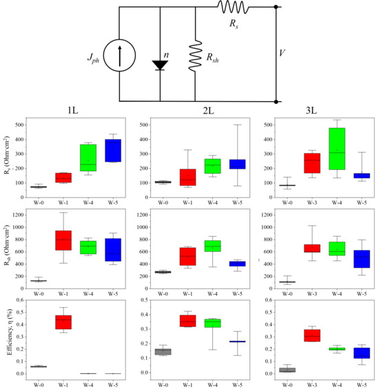
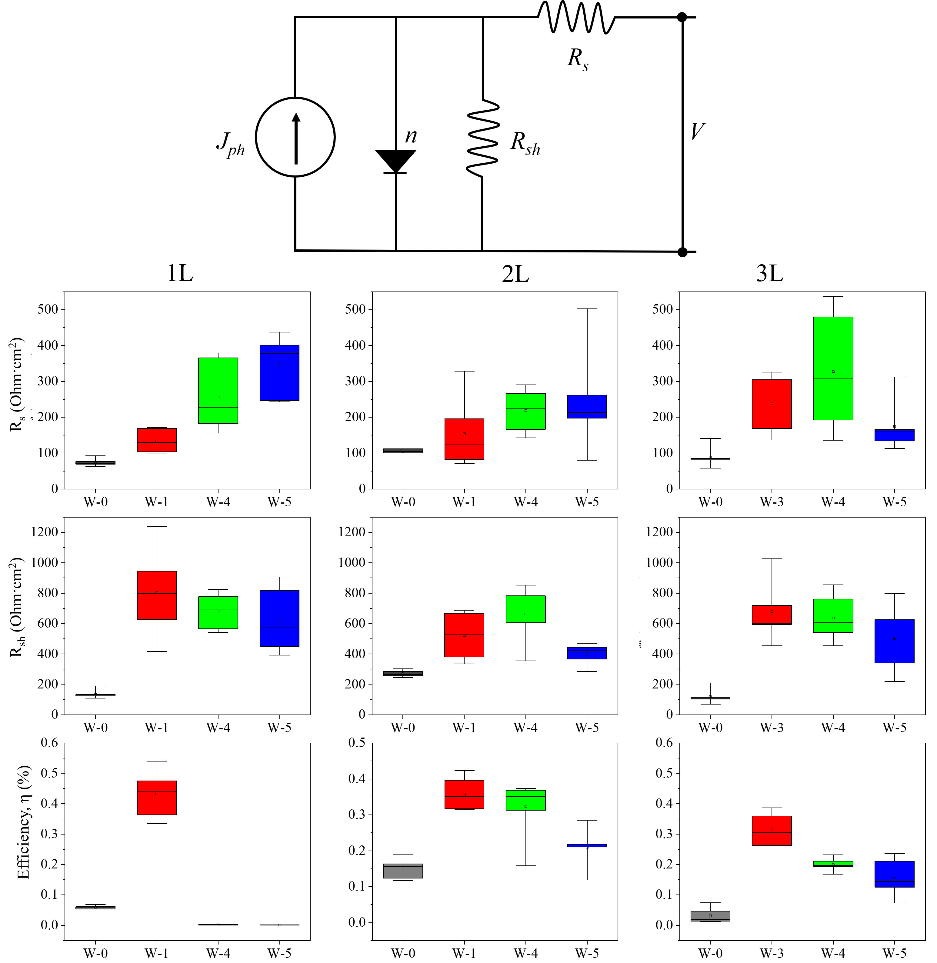
As the values of Jsc, Voc, and FF are modified, the shape of the J-V curve also undergoes modifications, including deformation, which is presented in the regions close to the intersection with both axes X and Y. This occurs in such a way that over time the curve acquires an S shape (see Figure S1). This behavior is frequently attributed to the electrical resistance effects, which are additional parameters that must be considered in evaluating the device’s performance. The equivalent circuit of a solar cell is composed of two types of resistors corresponding to the series and shunt resistances, as shown in Figure 7. The series resistance induces a voltage drop, as it divides the applied voltage; therefore, a high value of Rs produces a decreased drop voltage diode, while Rsh shows the opposite tendency. Their values can be obtained from the J-V curve, and it is well-known that series resistance has a strong influence on the FF, impacting the shape of the curve and causing a reduction in efficiency [14,29,30,31]. The Rs value mainly originated from the contact resistance between the materials that make up the photovoltaic device.
Figure 7.
Equivalent circuit and box chart of Rs, Rsh, and efficiency of the OSCs.
Figure 7 shows the behavior of both series and shunt resistance in a standard box chart. Rs increases as time passes, reaching values between 80 and 400 Ohm, while Rsh decreases as the number of weeks since the device’s manufacture increases. Increasing the thickness of the active layer from 1L to 2L produces more stable devices, as evidenced by Rs, Rsh, and the efficiency values obtained. This last registered a maximum value of 0.5%. However, for P3HT:PCBM thicknesses greater than 120 nm, there was a noticeable degradation in all electrical parameters.
As shown above, the active layer with a thickness of around 120 nm exhibited superior performance, as higher values reduce the OSC’s photoconversion. This effect can be attributed to the fact that, as the contact thickness increases, charge carriers must travel longer distances within the contact, and given their low mobility, thick layers are counterproductive to achieving optimal performance.
2.5. Metal Contact Effect
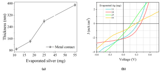
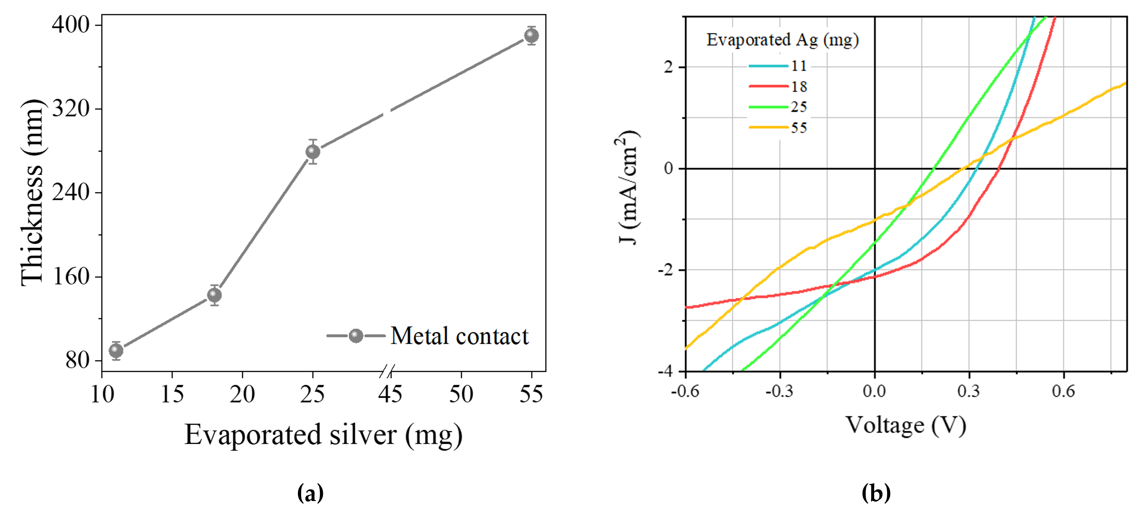
As shown above, the active layer, with a thickness of around 120 nm (2L), demonstrated superior performance in comparison to 1L and 3L. The photoconversion observed in 2L was notably higher than that in 1L and 3L. However, it is convenient to verify the thickness of the metal contact to ensure optimal PCE performance. Therefore, the amount of evaporated Ag for metal contact varied from 11 to 55 mg, corresponding to a Ag thickness of 90 to 390 nm (see Figure 8a). The J-V curves in Figure 8b indicate that a Ag metal contact with a thickness higher than 100 nm (18 mg of evaporated Ag) leads to a decrease in the current density and an increase in the series resistance. This phenomenon can be attributed to the fact that, as the thickness increases, charge carriers must travel a considerable distance within the contact. Given their limited mobility, thick metal layers are not the most effective solution to achieving optimal performance.
Figure 8.
(a) Variation in Ag thickness and (b) J-V curves of 2L solar cells as a function of the amount of evaporated silver.
In summary, the most favorable outcome of this study was achieved with an OSC fabricated with the 2L cell structure, reaching a conversion efficiency of 0.5%. Despite its modest value, this work reports valuable insights into the effects of thickness variations in the active layer and the Ag metal contact. This serves as a starting point for understanding their effects on the series resistance of the devices and, consequently, on the electrical parameters of the OSCs based on a P3HT:PCBM absorber layer, with the aim of contributing to the development of this kind of device.
Indeed, the highest efficiency achieved (0.5%) is below the values commonly reported for optimized P3HT:PCBM bulk heterojunction solar cells, where efficiencies above 3–5% are frequently obtained under highly optimized fabrication conditions [1,20]. However, it is important to emphasize that the main objective of the present study was not the optimization of device efficiency, but rather the systematic evaluation of the influence of active-layer thickness and Ag contact thickness on device behavior and temporal degradation. Consequently, the device architecture was intentionally kept relatively simple to isolate the effect of these parameters. In particular, the fabricated solar cells did not incorporate hole-transport layers such as PEDOT:PSS, MoO3, or LiF, which are widely recognized as essential components for improving interfacial energy alignment, reducing recombination losses, enhancing carrier selectivity, and facilitating charge extraction [24,32].
The absence of these interfacial engineering strategies is directly reflected in the electrical characteristics observed in the J-V curves obtained in this work. Compared with optimized P3HT:PCBM devices reported in the literature, our devices exhibit significantly lower short-circuit current densities (JSC), open-circuit voltages (VOC) below the typical range of 0.55–0.65 V, and modest fill factor (FF) values. In optimized devices, higher JSC values are generally associated with improved exciton dissociation and more efficient charge transport enabled by optimized donor–acceptor morphology and selective transport layers [33]. By contrast, the relatively low JSC values observed in our devices suggest limited carrier collection efficiency and increased recombination. Similarly, the reduced FF values and the shape of the J-V curves indicate the presence of significant series resistance (Rs) and non-ideal charge transport pathways, which become more evident during the degradation process. In fact, after the third week of fabrication, the increase in Rs strongly affected FF and PCE, indicating progressive deterioration of charge extraction and interfacial stability.
Additionally, the relatively low VOC values may also be related to imperfect energy-level alignment at the metal/organic interfaces due to the absence of interface-modifying layers. Previous studies have demonstrated that the inclusion of PEDOT:PSS and metal oxide buffer layers can substantially reduce contact resistance, improve built-in electric field distribution, and suppress recombination at the electrodes, thereby leading to considerable improvements in VOC, FF, and overall PCE [34]. Therefore, the low efficiency reported here should not be interpreted as an intrinsic limitation of the P3HT:PCBM system itself, but rather as a consequence of employing a non-optimized architecture specifically designed to investigate thickness-dependent optical absorption and degradation phenomena. Within this context, the observed trends remain scientifically relevant, particularly because the optical transmittance results demonstrated enhanced light absorption with increasing active-layer thickness, while the temporal evolution of the J-V parameters provided valuable information regarding possible degradation processes dominated by series resistance effects.
3. Materials and Methods
3.1. The Solar Cell Fabrication
The OSCs were fabricated in an inverted configuration composed of Ag/P3HT:PCBM/TiO2/ITO/glass. The substrates used in this study were commercial glasses (1 × 1 in2) from Delta Technologies (Loveland, CO, USA) coated with indium tin oxide (ITO). The substrates were cleaned in an ultrasonic bath, immersed successively in soapy water, acetone, methanol, and ethanol for 8 min each. Subsequently, the substrates were rinsed with distilled water and dried with air. Then, a thin film of titanium dioxide (TiO2) with a thickness of approximately 50 nm was deposited onto the ITO/glass substrates using the ultrasonic spray pyrolysis (USP) technique at 350 °C.
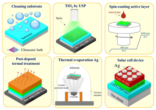
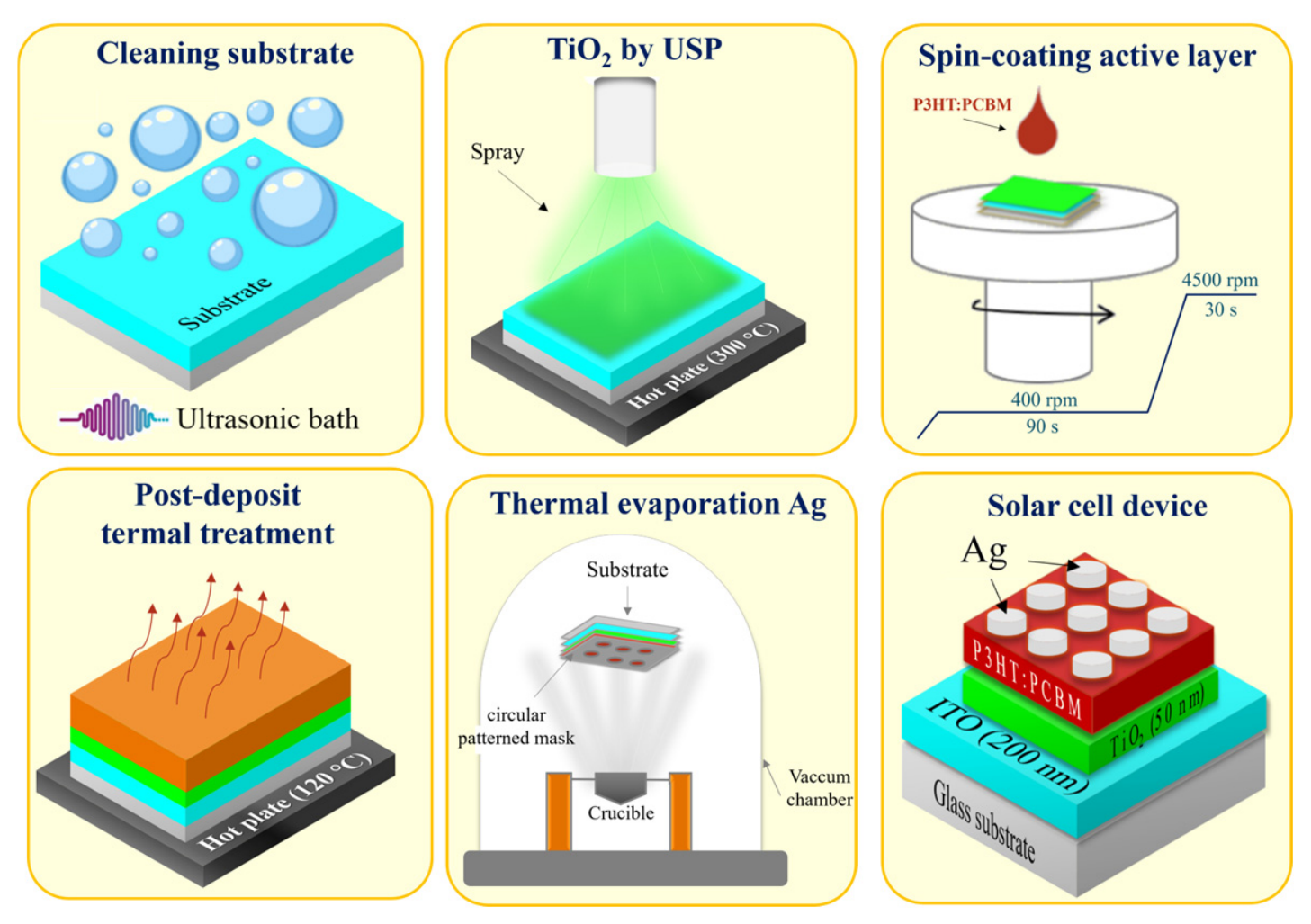
P3HT and PCBM were purchased from Sigma-Aldrich (St. Louis, MO, USA) with a purity higher than 99%. Both were dissolved in chlorobenzene (Sigma-Aldrich) at a weight ratio of 1:1 and a concentration of 20 mg/mL. The mixture was stirred in a glycerin bath at 53.5 °C for 18 h. A dynamic spin-coating method was employed to deposit the active layer (75–160 nm) onto the TiO2/ITO/glass structure, using two speed ramps. The first ramp was set at 400 rpm for 90 s, and the second ramp was set at 4500 rpm for 30 s. Subsequently, a post-deposition thermal treatment at 120 °C for 20 min was performed. Finally, Ag was evaporated as a metal electrode using a circular pattern mask with an area of 6 mm2. Figure 9 shows the process fabrication diagram and final device structure.
Figure 9.
Schematic representation of the solar cell process fabrication.
3.2. Characterization
The structural properties of the OSC layers were measured by X-ray diffraction (XRD) and Raman spectroscopy. Grazing incident X-ray diffraction (GI-XRD) patterns were recorded using a Siemens D-5000 diffractometer (Siemen, Munich, Germany). The measurement was performed in 2θ sweeping from 20° to 60° under a scan speed of 0.02°/3 s using a Cu kα tube (λ = 1.5406 Å) with an incident angle of 3°. Raman measurements were performed using a WITEC Alpha 300 Confocal Raman Microscope (WITEC, Ulm, Germany) at room temperature with an Ar+ ion laser, operating at an excitation wavelength of 632 nm. The optical transmittance of the device structure, before depositing the Ag contact layer, was measured over the wavelength range of 250–900 nm using a DH 2000 Ocean Optics spectrometer (Ocean Optics, Orlando, FL, USA). SEM images were obtained using a JEOL JSM 7600F Field Emission Scanning Electron Microscope (FE-SEM) (JEOL, Tokyo, Japan). The thickness of the P3HT:PCBM active layer was estimated by reflectance spectra with a Filmetrics F20 thin-film analyzer (KLA, San Diego, CA, USA), and cross-section SEM images were used to corroborate the results.
The photovoltaic device’s performance was monitored by J-V curve measurements, which were carried out in a home-made system using a Keithley 2450 source-meter (Keithley, Beaverton, OR, USA) under light irradiation from a halogen lamp. Evolution of J-V curves with time was evaluated over five weeks, analyzing the behavior of the electrical parameters of the fabricated OSCs.
4. Conclusions
Cell structures composed of Ag/P3HT:PCBM/TiO2/ITO/glass were successfully fabricated, and the presence of each material was corroborated by XRD and Raman spectroscopy measurements. The thickness of the P3HT:PCBM active layer in organic solar cells was modulated by varying the number of spin-coated layers (one to three), yielding values between 75 and 160 nm. Optical transmittance spectra demonstrated that increasing active layer thickness enhances light absorption, while J-V measurements revealed the corresponding effects on device performance. Electrical parameters monitored over five weeks showed that degradation begins after the third week, primarily due to increased series resistance, which negatively impacts Voc, fill factor (FF), and overall efficiency. Among the tested devices, the two-layer (2L) configuration achieved the most favorable outcome, with a conversion efficiency of 0.5%.
Although the objective of this work was not to develop state-of-the-art solar cells, the reported results provide valuable insights into how active layer thickness and Ag contact influence series resistance and, consequently, the electrical behavior of P3HT:PCBM-based OSCs. This study establishes a foundation for further optimization strategies aimed at improving the stability and efficiency of organic solar cells.
Supplementary Materials
The following supporting information can be downloaded at https://www.mdpi.com/article/10.3390/inorganics14060157/s1. Figure S1: Evolution over time of J-V curves of OSCs based on 1L, 2L, and 3L cell structures.
Author Contributions
Conceptualization, E.H.-R.; methodology, M.L.-P.; validation, I.R. and D.M.-R.; formal analysis, E.F. and E.H.-R.; investigation, I.R. and D.M.-R.; data curation, M.L.-P. and R.M.-F.; writing—original draft preparation, M.L.-P.; writing—review and editing, I.R., R.M.-F., E.F., D.M.-R. and E.H.-R.; visualization, E.F.; supervision, E.H.-R.; project administration, E.H.-R.; funding acquisition, E.H.-R. All authors have read and agreed to the published version of the manuscript.
Funding
This research was funded by CONACYT-México under the PDCPN-2015 (grant number 28) and SECIHTI-México by the postdoctoral scholarship of M.L-P. (CVU: 556332).
Institutional Review Board Statement
Not applicable.
Informed Consent Statement
Not applicable.
Data Availability Statement
The raw data supporting the conclusions of this article will be made available by the authors on request.
Acknowledgments
M. Loeza-Poot acknowledges SECIHTI-México for a postdoctoral scholarship (CVU: 556332) at the Mechanical Engineering Department of Universidad de Guanajuato. The authors acknowledge the Laboratorio Nacional de Nano y Biomateriales, Cinvestav-Unidad Mérida, for providing access to laboratory facilities within the projects FOMIX-Yucatán 2008-108160. The authors thank V. Rejón for technical support and useful discussions.
Conflicts of Interest
The authors declare no conflicts of interest.
References
- Grancharov, G.; Atanasova, M.-D.; Kalinova, R.; Gergova, R.; Popkirov, G.; Dikov, C.; Sendova-Vassileva, M. Flexible Polymer–Organic Solar Cells Based on P3HT:PCBM Bulk Heterojunction Active Layer Constructed under Environmental Conditions. Molecules 2021, 26, 6890. [Google Scholar] [CrossRef] [Scilit]
- Yu, G.; Gao, J.; Hummelen, J.C.; Wudl, F.; Heeger, A.J. Polymer Photovoltaic Cells: Enhanced Efficiencies via a Network of Internal Donor-Acceptor Heterojunctions. Science 1995, 270, 1789–1791. [Google Scholar] [CrossRef] [Scilit]
- Thompson, B.C.; Fréchet, J.M.J. Polymer–Fullerene Composite Solar Cells. Angew. Chem. Int. Ed. 2008, 47, 58–77. [Google Scholar] [CrossRef] [Scilit] [PubMed]
- Li, Y.; Huang, W.; Zhao, D.; Wang, L.; Jiao, Z.; Huang, Q.; Wang, P.; Sun, M.; Yuan, G. Recent Progress in Organic Solar Cells: A Review on Materials from Acceptor to Donor. Molecules 2022, 27, 1800. [Google Scholar] [CrossRef] [Scilit]
- Ghosekar, I.C.; Patil, G.C. Review on Performance Analysis of P3HT:PCBM-Based Bulk Heterojunction Organic Solar Cells. Semicond. Sci. Technol. 2021, 36, 045005. [Google Scholar] [CrossRef] [Scilit]
- Lattante, S. Electron and Hole Transport Layers: Their Use in Inverted Bulk Heterojunction Polymer Solar Cells. Electronics 2014, 3, 132–164. [Google Scholar] [CrossRef] [Scilit]
- Abdallaoui, M.; Sengouga, N.; Chala, A.; Meftah, A.F.; Meftah, A.M. Comparative Study of Conventional and Inverted P3HT: PCBM Organic Solar Cell. Opt. Mater. 2020, 105, 109916. [Google Scholar] [CrossRef] [Scilit]
- Wright, M.; Uddin, A. Organic—Inorganic Hybrid Solar Cells: A Comparative Review. Sol. Energy Mater. Sol. Cells 2012, 107, 87–111. [Google Scholar] [CrossRef] [Scilit]
- Li, Y.; Xu, G.; Cui, C.; Li, Y. Flexible and Semitransparent Organic Solar Cells. Adv. Energy Mater. 2018, 8, 1701791. [Google Scholar] [CrossRef] [Scilit]
- Lu, S.; Sun, Y.; Ren, K.; Liu, K.; Wang, Z.; Qu, S. Recent Development in ITO-Free Flexible Polymer Solar Cells. Polymers 2017, 10, 5. [Google Scholar] [CrossRef] [Scilit]
- Poortmans, J.; Arkhipov, V. (Eds.) Thin Film Solar Cells: Fabrication, Characterization and Applications, 1st ed.; Wiley: Hoboken, NJ, USA, 2006. [Google Scholar]
- Hädrich, M.; Kraft, C.; Löffler, C.; Metzner, H.; Reislöhner, U.; Witthuhn, W. Pathways to Thin Absorbers in CdTe Solar Cells. Thin Solid Film. 2009, 517, 2282–2285. [Google Scholar] [CrossRef] [Scilit]
- Peña, J.L.; Arés, O.; Rejón, V.; Rios-Flores, A.; Camacho, J.M.; Romeo, N.; Bosio, A. A Detailed Study of the Series Resistance Effect on CdS/CdTe Solar Cells with Cu/Mo Back Contact. Thin Solid Film. 2011, 520, 680–683. [Google Scholar] [CrossRef] [Scilit]
- Shen, Y.; Li, K.; Majumdar, N.; Campbell, J.C.; Gupta, M.C. Bulk and Contact Resistance in P3HT:PCBM Heterojunction Solar Cells. Sol. Energy Mater. Sol. Cells 2011, 95, 2314–2317. [Google Scholar] [CrossRef] [Scilit]
- Pysch, D.; Mette, A.; Glunz, S.W. A Review and Comparison of Different Methods to Determine the Series Resistance of Solar Cells. Sol. Energy Mater. Sol. Cells 2007, 91, 1698–1706. [Google Scholar] [CrossRef] [Scilit]
- Duraisamy, N.; Muhammad, N.M.; Hyun, M.-T.; Choi, K.-H. Structural and Electrical Properties of P3HT:PCBM/PEDOT:PSS Thin Films Deposited through Electrohydrodynamic Atomization Technique. Mater. Lett. 2013, 92, 227–230. [Google Scholar] [CrossRef] [Scilit]
- Castillo, N.; Olguín, D.; Conde-Gallardo, A.; Jiménez-Sandoval, S. Structural and Morphological Properties of TiO2thin Films Prepared by Spray Pyrolysis. Rev. Mex. Física 2004, 50, 382–387. [Google Scholar]
- Alaya, Y.; Souissi, R.; Toumi, M.; Madani, M.; El Mir, L.; Bouguila, N.; Alaya, S. Annealing Effect on the Physical Properties of TiO2 Thin Films Deposited by Spray Pyrolysis. RSC Adv. 2023, 13, 21852–21860. [Google Scholar] [CrossRef] [Scilit] [PubMed]
- Kumar, S.; Kumar, M.; Rathi, S.; Yadav, A.; Upadhyaya, A.; Gupta, S.K.; Singh, A. Study of P3HT/PCBM Morphology Using Raman Spectroscopy; AIP Publishing LLC.: Melville, NY, USA, 2018; p. 100074. [Google Scholar]
- Shaban, M.; Benghanem, M.; Almohammedi, A.; Rabia, M. Optimization of the Active Layer P3HT:PCBM for Organic Solar Cell. Coatings 2021, 11, 863. [Google Scholar] [CrossRef] [Scilit]
- Cook, S.; Katoh, R.; Furube, A. Ultrafast Studies of Charge Generation in PCBM:P3HT Blend Films Following Excitation of the Fullerene PCBM. J. Phys. Chem. C 2009, 113, 2547–2552. [Google Scholar] [CrossRef] [Scilit]
- Ulum, M.S.; Sesa, E.; Kasman; Belcher, W. The Effect of Active Layer Thickness on P3HT:PCBM Nanoparticulate Organic Photovoltaic Device Performance. J. Phys. Conf. Ser. 2019, 1242, 012025. [Google Scholar] [CrossRef] [Scilit]
- Vlahović, J.; Stanojević, M.; Gojanović, J.; Melancon, J.; Sharma, A.; Živanović, S. Thickness Dependent Photocurrent Spectra and Current-Voltage Characteristics of P3HT:PCBM Photovoltaic Devices. Opt. Express 2021, 29, 8710. [Google Scholar] [CrossRef] [Scilit]
- Balraj, B.; Raja, M.; Prabhu, T.G.V.; Balaji, M.; Chandrasekaran, J.; Nagarajan, S.K.; Bharathi, M.; Lee, S.; Sivakumar, C. A Critical Review on Decade Progress and Future Prospects of P3HT:PCBM Bulk Heterojunction Solar Cells. Sol. Energy 2025, 297, 113574. [Google Scholar] [CrossRef] [Scilit]
- Qi, B.; Wang, J. Open-Circuit Voltage in Organic Solar Cells. J. Mater. Chem. 2012, 22, 24315. [Google Scholar] [CrossRef] [Scilit]
- Lee, W.H.; Chuang, S.Y.; Chen, H.L.; Su, W.F.; Lin, C.H. Exploiting Optical Properties of P3HT:PCBM Films for Organic Solar Cells with Semitransparent Anode. Thin Solid Film. 2010, 518, 7450–7454. [Google Scholar] [CrossRef] [Scilit]
- Li, P.; Wang, X.; Huang, H.; Yang, X.; Zhou, T.; Jiang, Z. The Effect of Thermal Annealing on Defect States, Light Intensity and Photocurrent of Organic Solar Cells. Optik 2022, 265, 169488. [Google Scholar] [CrossRef] [Scilit]
- Domanski, A.L.; Lieberwirth, I.; Sengupta, E.; Landfester, K.; Butt, H.-J.; Berger, R.; Rauh, J.; Dyakonov, V.; Deibel, C. Effect of Morphological Changes on Presence of Trap States in P3HT:PCBM Solar Cells Studied by Cross-Sectional Energy Filtered TEM and Thermally Stimulated Current Measurements. J. Phys. Chem. C 2013, 117, 23495–23499. [Google Scholar] [CrossRef] [Scilit]
- Sze, S.M.; Ng, K.K. Physics of Semiconductor Devices, 1st ed.; Wiley: Hoboken, NJ, USA, 2006. [Google Scholar]
- Xue, J.; Uchida, S.; Rand, B.P.; Forrest, S.R. 4.2% Efficient Organic Photovoltaic Cells with Low Series Resistances. Appl. Phys. Lett. 2004, 84, 3013–3015. [Google Scholar] [CrossRef] [Scilit]
- Servaites, J.D.; Yeganeh, S.; Marks, T.J.; Ratner, M.A. Efficiency Enhancement in Organic Photovoltaic Cells: Consequences of Optimizing Series Resistance. Adv. Funct. Mater. 2010, 20, 97–104. [Google Scholar] [CrossRef] [Scilit]
- P3HT:PCBM-Based Organic Solar Cells: Through Strategic ETL and HTL Material Selection—IOPscience. Available online: https://iopscience.iop.org/article/10.1088/2631-8695/ae30cf (accessed on 12 May 2026).
- Mkawi, E.M.; Al-Hadeethi, Y.; Bazuhair, R.S.; Yousef, A.s.; Shalaan, E.; Arkook, B.; Abdel-Daiem, A.M.; Bekyarova, E. Fabricated Cu2Zn SnS4 (CZTS) Nanoparticles as an Additive in P3HT: PCBM Active Layer for Efficiency Improvement of Polymer Solar Cell. J. Lumin. 2021, 240, 118420. [Google Scholar] [CrossRef] [Scilit]
- Hu, Z.; Zhang, J.; Hao, Z.; Zhao, Y. Influence of Doped PEDOT:PSS on the Performance of Polymer Solar Cells. Sol. Energy Mater. Sol. Cells 2011, 95, 2763–2767. [Google Scholar] [CrossRef] [Scilit]

Disclaimer/Publisher’s Note: The statements, opinions and data contained in all publications are solely those of the individual author(s) and contributor(s) and not of MDPI and/or the editor(s). MDPI and/or the editor(s) disclaim responsibility for any injury to people or property resulting from any ideas, methods, instructions or products referred to in the content. |
© 2026 by the authors. Licensee MDPI, Basel, Switzerland. This article is an open access article distributed under the terms and conditions of the Creative Commons Attribution (CC BY) license.