


Abstract
The versatile surface reconstruction mechanisms, tunable surface properties, and exceptional electron emission characteristics of SrTiO3 films have garnered significant research interest. In this study, SrTiO3 films were synthesized on n-Si(100) substrates via radio frequency magnetron sputtering. To evaluate the impact of thermal annealing, the as-deposited films underwent post-deposition annealing in an oxygen ambient at 600 °C, 800 °C, and 1000 °C for a duration of 2 h each. The structural, chemical, and secondary electron emission (SEE) characteristics of the SrTiO3 films were characterized as a function of their high thermal process. Post-deposition annealing induced a significant improvement in crystallinity, which directly correlated with a heightened SEE yield (SEY). Furthermore, composition analysis revealed a marked stoichiometric reconfiguration at the surface, with the Sr:Ti:O ratio evolving from 1:0.32:1.14 to 1:0.22:0.94, suggesting a move toward an Sr-O terminated surface. The Sr-O terminated surface inherent to these SrTiO3 films promotes efficient electron escape due to its reduced work function. Following a 1000 °C annealing process, the peak SEY undergoes a significant shift from 2.11 to 2.76, representing a thermal optimization of the SEE performance by approximately 30.8%. High-temperature annealing enhances the SEE performance of SrTiO3 films, validating their significant potential for electron multiplication applications. This study provides a scalable pathway for developing highly efficient SEE materials with optimized crystalline and surface properties.
1. Introduction
Strontium titanate (SrTiO3, denoted as STO), a typical ABO3-type perovskite oxide, has become a cornerstone material in the emerging field of oxide electronics due to its high dielectric constant, low leakage current, and excellent optical properties [1,2,3]. Due to their excellent bulk and surface properties, STO single crystals and polycrystalline thin films have been extensively researched for diverse applications, ranging from photocatalytic water splitting to their use as substrates for high-temperature superconductors and components in micro/nanoelectronics devices [4,5,6]. Furthermore, STO thin films exhibit multifunctional properties that are highly dependent on their unique surface structures, such as the specific (2 × 1) reconstruction of the STO (001) surface [7]. The physical properties of STO thin films are closely linked to their surface microstructure, morphology, chemical composition, and chemical states—all of which play a critical role in determining their electronic characteristics [8,9]. STO thin films exhibit distinct optoelectronic behaviors compared to their single-crystal counterparts [10]; variations in the oxidation states of metal cations serve as the primary cause of these property changes. The optical bandgap of STO films exhibits significant variability, ranging from 2.70 eV to 4.26 eV [11,12], as influenced by specific fabrication techniques and processing parameters. Ti-O or Sr-O terminated surfaces on STO can be achieved using various processes, including Ar+ etching, chemical etching, or annealing [13,14]. Vienna Ab initio simulation package (VASP) and experimental studies confirm that the work function of SrO-terminated STO (001) surfaces is generally lower than that of TiO2-terminated surfaces, regardless of whether the samples are subjected to thermal annealing or surface pretreatment [15,16]. STO thin films can be prepared using various deposition techniques, including atomic layer deposition [17], molecular beam epitaxy [18], metalorganic chemical vapor deposition [19], and RF magnetron sputtering [12]. Among these methods, RF magnetron sputtering stands out as a low-cost and efficient fabrication technique that is also suitable for wafer-scale mass production.
A common strategy for studying the electronic properties of STO involves high-temperature annealing to improve film crystalline quality and surface characteristics. This yields several important periodic reconstructions—e.g., (1 × 1), (2 × 2), and (4 × 4)—some of which have been analyzed in detail. In 2019, Kim et al. grew STO thin films via atomic layer deposition [20], applying rapid thermal annealing before depositing a main STO layer on the seed layer, thereby achieving in situ crystallization. In a low work function surface study in 2022, Kamaratos et al. exposed the STO (100) surface to water vapor and cesium vapor [21], observing the formation of cesium oxide (Cs2O), which further reduced the surface work function by up to 0.35 eV. In 2023, Hong et al. reported that anomalously strong and coherent secondary photoelectron emission was observed on the reconstructed SrTiO3 (100) surface following simple vacuum annealing [22]. The low work function surface formed after annealing is key to determining these unique secondary electron emission characteristics. In 2024, Pérez reported an optical bandgap of 3.06 eV after annealing STO thin films in a reducing atmosphere [23], and this sample demonstrated superior performance regarding overpotential, Tafel slope, and 24-h stability. In 2025, Chien synthesized SrTiO3/TiO2/TiN heterostructure films [24], annealing them under varying partial pressures of nitrogen and oxygen, and the introduction of oxygen vacancies at the interfaces promoted efficient charge separation and suppressed recombination during photoelectrochemical responses.
Although research on STO thin films has been quite extensive, most studies primarily focus on the relationships among preparation methods, surface reconstruction, film quality, and optical/electrochemical properties. There are few reports that research the secondary electron emission (SEE) of STO films. Within the field of SEE research, the use of surface microstructure [25,26,27,28] and functional coatings [29,30,31] to regulate surface SEE yield (SEY) is of paramount importance. For functional coatings engineering, typically, functional films such as titanium nitride are applied within particle accelerators to reduce SEY and further mitigate the risk of cloud effect occurrence [32,33]. Materials such as magnesium oxide possessing high SEY are frequently employed in the dynodes of electron multipliers to achieve efficient amplification of electronic signals within the device [30,34,35,36]. Moreover, materials possessing high SEY can also be effectively utilized in engineering scenarios where the suppression of electrostatic discharge is required [37,38]. Since STO is a ceramic material possessing a high bandgap (approximately 3.2 eV) [39], STO functional films are supposed to demonstrate efficacy in scenarios involving the modulation of SEY like various other functional coatings, such as in the dynode of photomultiplier tubes requiring high SEE capability [30].
In this study, we employed magnetron sputtering to deposit STO thin films on n-Si substrates, followed by annealing in an oxygen atmosphere, to characterize the film properties. For comparison, additional STO films were deposited under varying argon and oxygen partial pressures. The primary objective is to investigate how these different sputtering and annealing conditions affect the secondary electron emission characteristics of the STO thin films.
2. Results and Discussion
2.1. Film Morphology of the STO Films
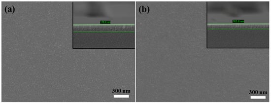
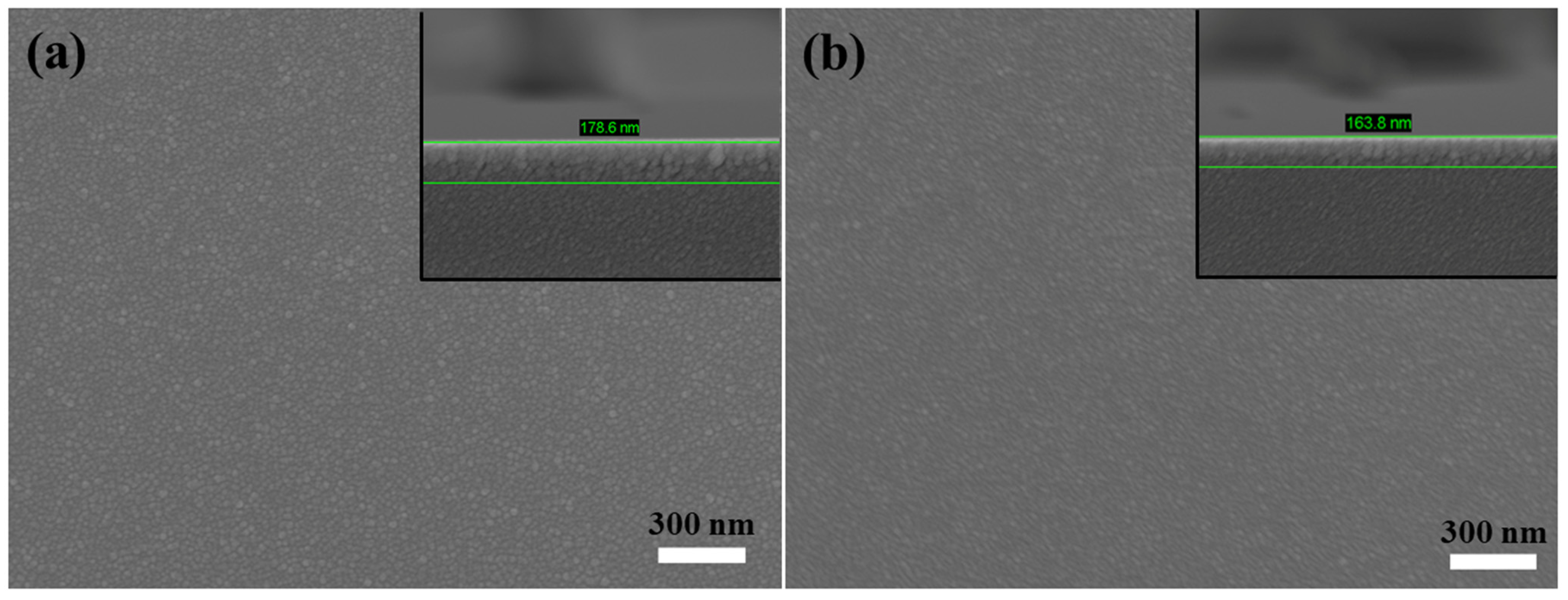
The surface morphology of the STO thin films, as characterized by plan-view field emission scanning electron microscopy (FESEM) [23,40], is illustrated in Figure 1. Figure 1a depicts the as-deposited state, while Figure 1b illustrates the morphological changes following a 2 h annealing treatment at 1000 °C under an oxygen atmosphere. The STO film exhibited a thickness reduction from 178.6 nm in the as-deposited state to 163.8 nm following high-temperature annealing. This volumetric contraction of approximately 8.3% is fundamentally attributed to thermal densification and the elimination of residual porosity inherent in room-temperature magnetron-sputtered oxide films. A detailed examination of the STO thin-film morphology reveals that the films remain dense both before and after annealing, with surface grain sizes in the range of several tens of nanometers. The thermal treatment did not significantly alter the overall surface morphology. It is inferred that while annealing promoted Ostwald ripening [41,42]—thereby improving crystalline quality and reducing surface energy—the surface remained continuous and devoid of observable cracks.
Figure 1.
FESEM images of STO thin film on n-Si substrates: (a) as-deposited (unannealed) and (b) annealed. The inset in the upper right corner of (a,b), confirm a thickness reduction from 178.6 nm (as-deposited) to 163.8 nm (post-annealing).
2.2. Elemental Composition of the STO Films
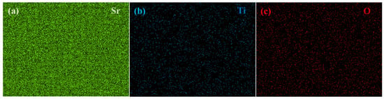
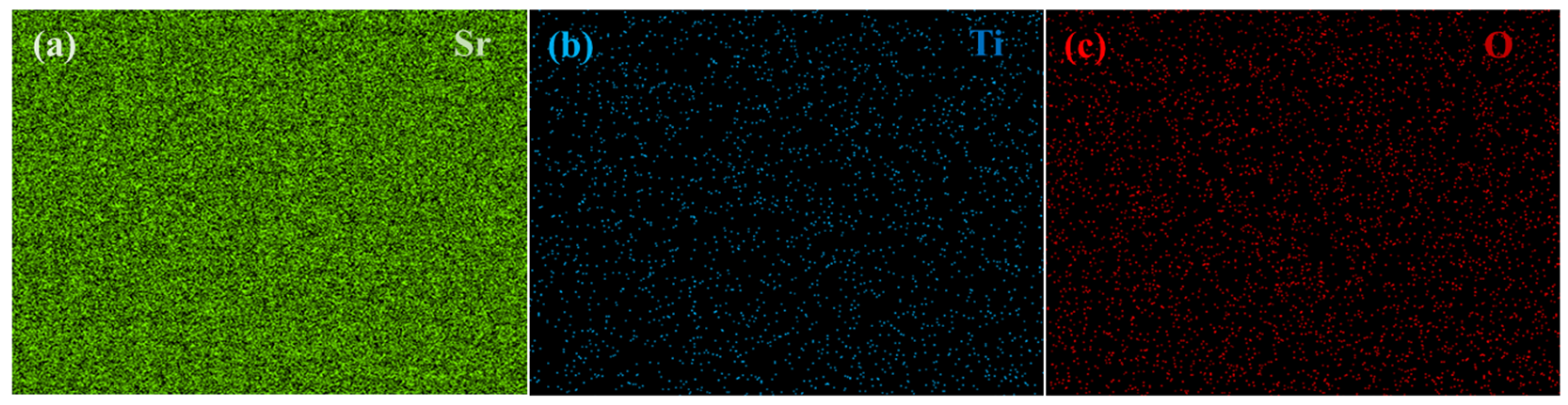
In addition to morphological characterization, we employed energy-dispersive X-ray spectroscopy (EDS) to examine the elemental distribution across the surface of the prepared STO films, as illustrated in Figure 2. Figure 2a–c, respectively, show the elemental densities of Sr, Ti, and O within the EDS testing regions. The distribution results of planar elements in Figure 2 show the uniform distribution of the three elements within the test are, and reveal a high density of Sr, while Ti and O exhibit relatively low densities. This indicates that the Sr content is markedly higher than that of Ti and O. Furthermore, based on the operating principle of EDS [43,44], we understand that its detection depth ranges from several hundred nanometers to the micrometer scale. Consequently, the elemental composition results measured in Figure 2 also indirectly indicate that the thickness of the prepared STO film is comparable to the EDS detection depth at accelerating voltage of 5 kV.
Figure 2.
EDS elemental mapping images of (a) Sr, (b) Ti, and (c) O.
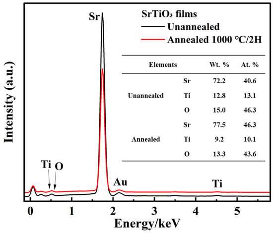
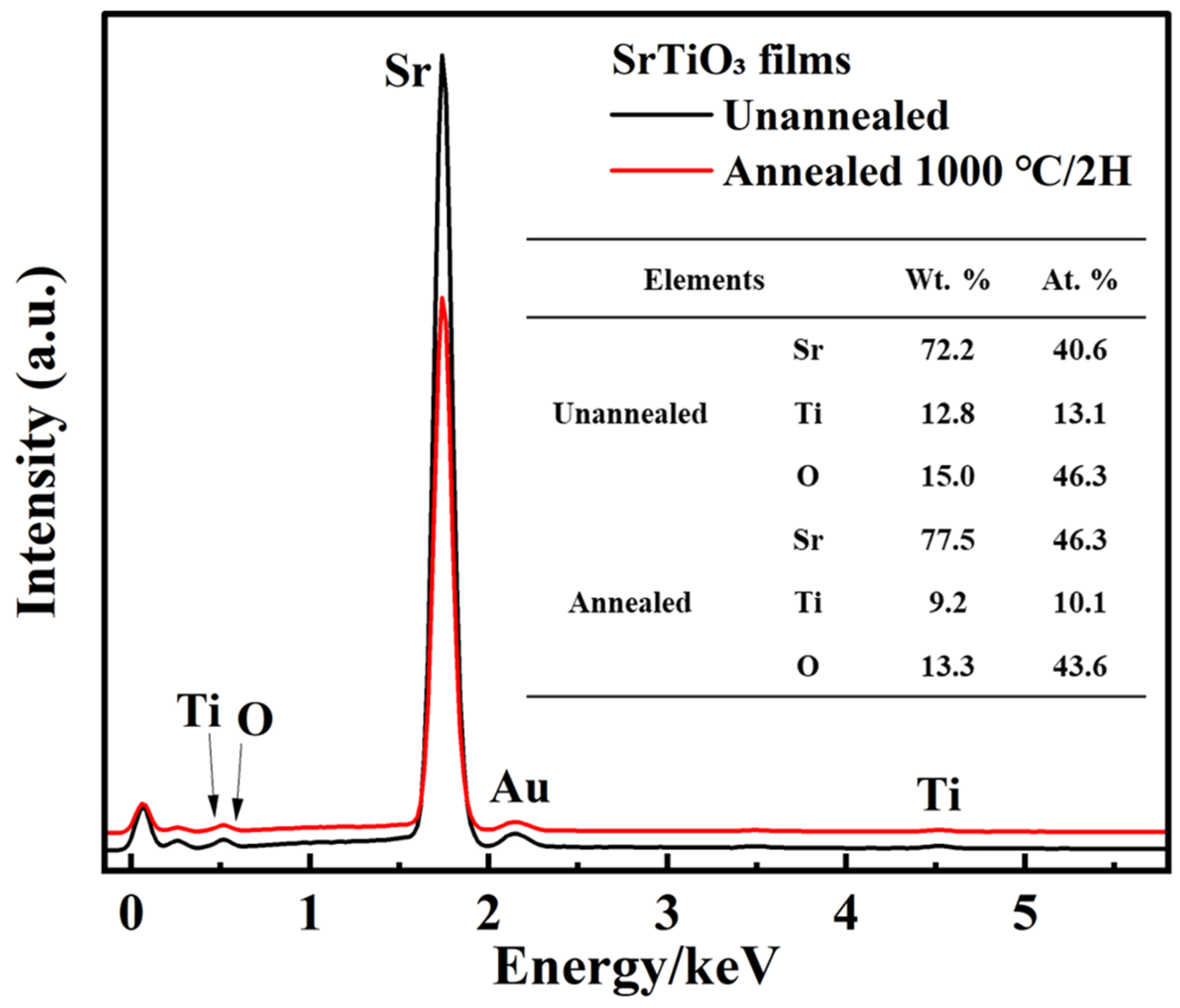
In addition to the elemental distribution density, we also employed EDS to determine the relative abundance of each element of the STO perovskite material after annealing, including the EDS spectra and elemental percentages, as shown in Figure 3. In Figure 3, the spectrum exhibits prominent peaks at the characteristic K-shell emission positions for Sr, Ti, and O. The quantitative elemental data are summarized in the inset table. The mass fractions (Wt. %) for Sr, Ti, and O—before and after annealing—were 72.2%/77.5%, 12.8%/9.2%, and 15.0%/13.3%, respectively. These correspond to atomic percentages (At. %) of 40.6%/46.3% (Sr), 13.1%/10.1% (Ti), and 46.3%/43.6% (O). Strontium and Titanium are major metal elements, and their relative atomic ratios should therefore be precise within a ±1.0% range; however, oxygen (a light element) typically has a much higher relative error a ±5.0% due to low X-ray yield and high absorption. The elemental atomic ratio in the unannealed sample (1:0.32:1.12) deviates sharply from ideal SrTiO3, revealing substantial Ti and O vacancies. After annealing, this ratio shifts to 1:0.22:0.93, demonstrating that high-temperature treatment exacerbates the surface Ti and O loss and increases the stoichiometric deviation. The elemental stoichiometry of sputtered STO films inherently deviates from the ideal 1:1:3 single-crystal ratio due to non-congruent sputtering. Multi-component perovskite targets rarely exhibit equal ejection rates; lighter species and those with lower binding energies are preferentially sputtered. While theoretical sputtering yields for Ti often exceed those of strontium Sr due to superior mass-matching with Ar, several synergistic factors contribute to the measured Sr enrichment:
Figure 3.
The corresponding EDS spectrum for these samples. The inset in image presents the EDS quantification data, showing the mass percentage (Wt. %) and atomic percentage (At. %) for Sr, Ti, and O, respectively.
- (1)
- Instrumental Sensitivity: The higher X-ray emission efficiency of heavier cations (Sr) can influence quantitative software results, particularly in standardless models where ZAF correction algorithms may carry inherent analytical uncertainties.
- (2)
- Target Stoichiometry: The initial SrTiO3 target may exhibit a slight Sr-rich bias, which is propagated during the deposition process.
- (3)
- Non-Congruent Transport: Specific sputtering parameters, such as low working pressures or elevated substrate temperatures, may modulate the sticking coefficients and re-sputtering rates, favoring Sr-incorporation over Ti.
- (4)
- Thermal Annealing: During annealing, the relative instability of Ti leads to preferential migration and volatilization, facilitating the formation of a stable SrOx-rich surface layer.
Given that the EDS interaction range significantly exceeds the thin-film thickness, the reported data represent a volumetric average of the Sr-rich surface and the stoichiometric bulk. Thus, the observed Sr > Ti ratio is a physical manifestation of integrated Ti-depletion rather than a preparation artifact. This fundamental alteration of the surface chemical state is likely responsible for the modified electronic properties and electron emission characteristics of the films.
In fact, under high-temperature oxidizing conditions, Ti species are prone to volatilization via the formation of TiO2 or volatile suboxides, especially at high-energy sites like grain boundaries. This process, coupled with thermally induced oxygen vacancies or chemical interactions with the underlying n-Si substrate, fundamentally alters the surface stoichiometry. The formation of a SrO–rich surface termination after thermal treatment is proposed to account for the signal attenuation of Ti, as the enriched overlayer limits the depth-sensitive detection of titanium cations. In 2019, investigations by Chambers and Sushko [16], utilizing UPS experiments and DFT calculations, revealed that the work function of STO (001) surfaces is highly termination-dependent: 3.1~3.6 eV for SrO-terminated surfaces and 4.5~4.8 eV for TiO2-terminated surfaces. A Sr-rich surface significantly reduces the samples’ effective work function, representing one of the most viable strategies for enhancing the SEE of STO films. Additionally, trace peaks associated with adsorbed carbon and the gold coating (sputtered for conductivity) were detected. The EDS elemental mapping of the annealed STO thin film in Figure 2a–c demonstrates a uniform spatial distribution of Sr, Ti, and O across the surface. Qualitatively, the higher image contrast observed in the Sr map suggests a significantly greater signal intensity compared to those of Ti and O, which aligns with the Sr enrichment observed in the quantitative analysis.
2.3. Phase Structure of the STO Films
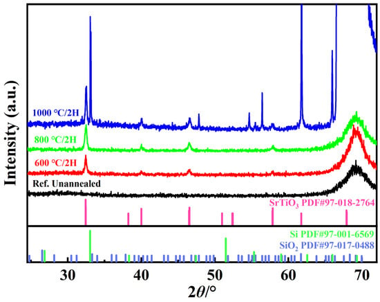
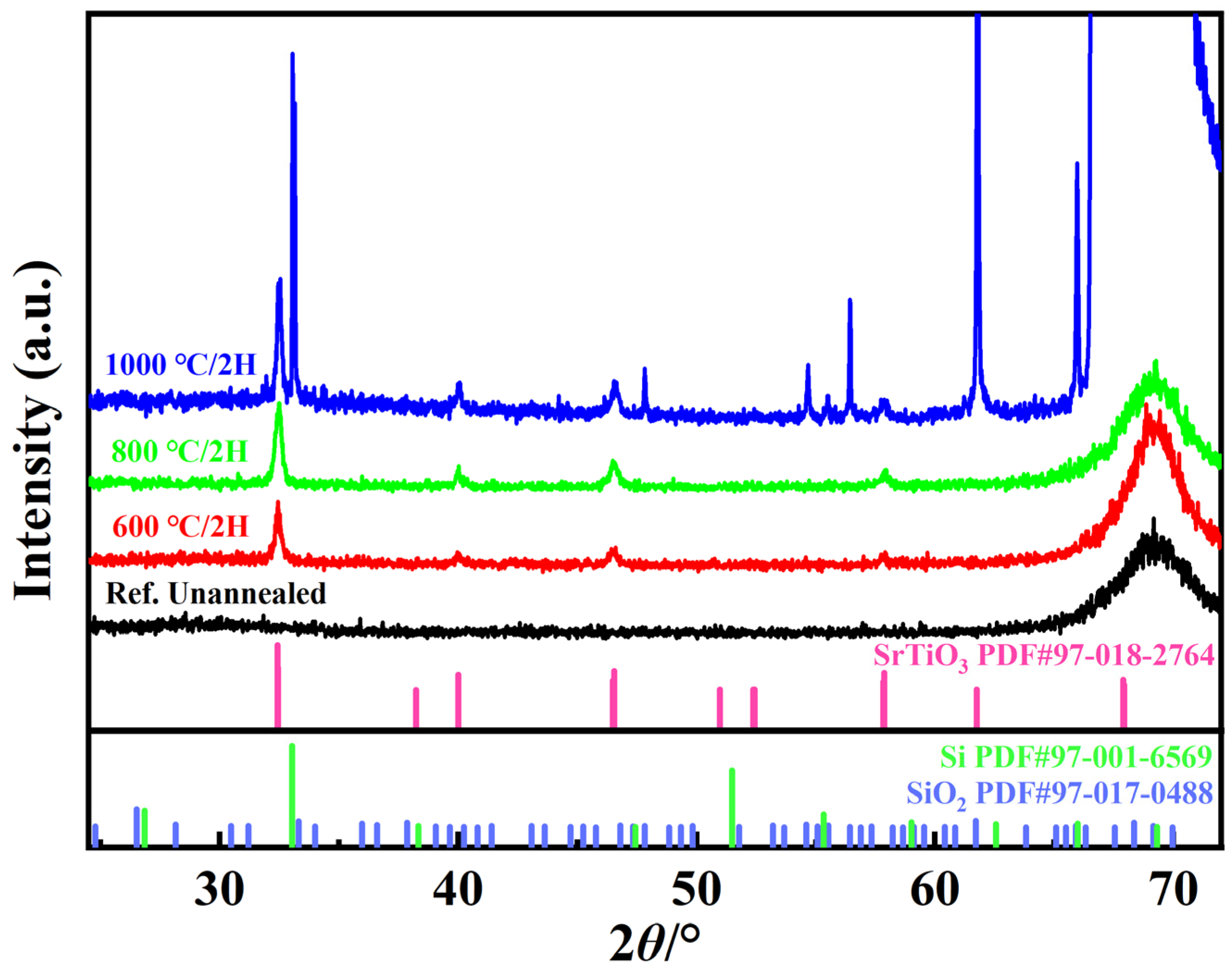
The crystallinity and phase evolution of the thin films are strictly governed by the deposition parameters and post-deposition annealing temperatures. Therefore, to further characterize the phase structure changes in STO films before and after annealing, we employed X-ray diffraction (XRD) techniques to examine the phase structure of the STO films. Figure 4 illustrates the XRD patterns for the as-deposited and thermally treated STO films. In the as-deposited state, the room-temperature-sputtered samples exhibited a purely amorphous phase, as corroborated by the reference patterns. Subsequent annealing at 600 °C, 800 °C, and 1000 °C in an oxygen (O2) ambient for two hours induced a progressive enhancement in crystallinity, facilitating a transition into a well-defined polycrystalline state. Compared to the amorphous as-deposited state, the emergence of sharp diffraction peaks between 30° and 70° signifies the development of a well-ordered crystalline phase. On the one hand, the polycrystalline structure was indexed to tetragonal STO (JCPDS PDF card No.: 97-018-2764), with characteristic reflections from the (112), (200), (202), (004), (220), (204), (312), and (321) planes identified at 2θ positions of 32.4°, 32.4°, 40.0°, 46.4°, 46.5°, 57.8°, 57.8°, and 61.7°, respectively. Notably, the proximity diffraction peaks from the (112) and (200) planes, as well as those from the (204) and (312) planes, results in peak overlap that precludes their individual resolution within the measured XRD patterns. On the other hand, the diffraction features observed at 33.0° and 65.9° in the sample annealed at 1000 °C are indexed to the n-Si substrate (JCPDS PDF card No.: 97-017-0488). Given the high-temperature treatment in an oxygen ambient, we have evaluated and subsequently ruled out the precipitation of titanium oxide (TiOx) or strontium oxide (SrOx) phases. Instead, the reflections identified at 47.8°, 54.6°, 55.5°, 56.4°, and 65.9° are attributed to the interfacial formed SiO2 layer (JCPDS PDF card No.: 97-017-0488) formed via thermal oxidation of the substrate. The broad diffraction envelope observed between 66.1° and 72° in Figure 4 results from the overlapping diffraction peaks from the n-Si substrate, the interfacial SiO2 layer, and the STO film. This high peak intensity, combined with the high degree of spectral congestion, precludes the precise resolve of individual peak positions within this range. Overall, the XRD results confirm that the crystalline quality of the room-temperature-sputtered STO films is significantly enhanced through high-temperature annealing in an oxygen ambient.
Figure 4.
XRD patterns of as-synthesized and annealed STO films (600 °C, 800 °C, and 1000 °C) in O2 for 2 h.
2.4. SEE Properties of the STO Films
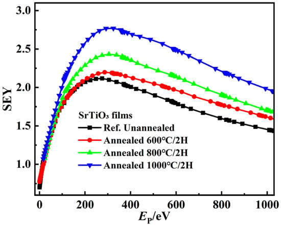
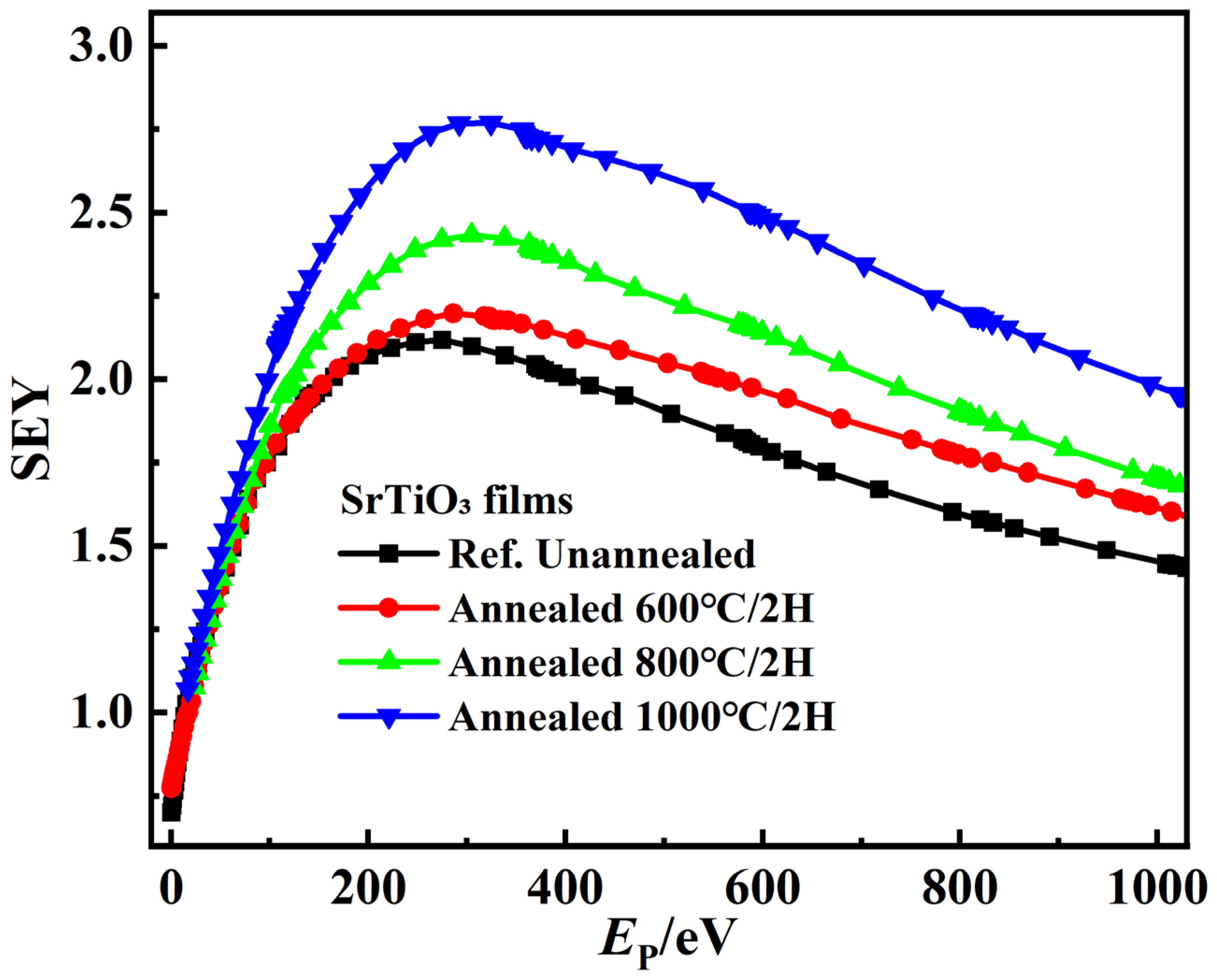
The impact of the post-deposition annealing process under an O2 atmosphere on the SEE properties of STO films was investigated through SEY measurements. The data confirm that thermal processing markedly improved the secondary electrons emission efficiency of the films. As illustrated in Figure 5, the SEY values exhibit a clear upward shift following the annealing treatment, far exceeding the SEY of the amorphous as-deposited samples. The critical parameters of the SEY profiles, specifically the optimal primary electron energy (Epm) and maximum yield (δm), are tabulated in Table 1 for the as-deposited and thermally treated STO thin films. The initial SEY curve’s peak of the as-deposited STO film, defined by (Ep,m, δm), was recorded at (260 eV, 2.11). Following thermal treatment in an oxygen ambient at 600 °C for two hours, the SEE characteristics exhibited a marginal enhancement to (306 eV, 2.19), representing a yield increase (Δδ%) of approximately 3.8%. Notably, the STO films annealed at 800 °C and 1000 °C demonstrate substantial performance further enhancements; their SEY peaks shifted to (304 eV, 2.43) and (305 eV, 2.76), respectively, corresponding to Δδ% improvements of 15.2% and 30.8% relative to the as-deposited state. While δm increases, Epm remains relative stable at approximately 305 eV, suggesting that the secondary electron escape depth in the STO thin films undergoes negligible variation. Consequently, the observed enhancement is primarily attributed to improved long-range crystalline order and refined surface conditions, which facilitate more efficient electron transport to the surface and a higher probability of emission following generation. Thermal treatment in an oxygen ambient effectively decontaminates the surface and mitigates structural defects, thereby optimizing the overall SEE efficiency. The results provide a scalable pathway for improving the performance of materials with modest inherent SEY, thereby broadening their suitability for high-performance secondary electron multiplication applications.
Figure 5.
SEY characteristics of STO films on n-Si substrates. SEY curves are presented for samples in the as-deposited (unannealed) state and annealed temperatures at 600 °C, 800 °C, and 1000 °C.
Table 1.
SEY characteristics of as-synthesized and annealed STO films.
3. Experimental Methodology
3.1. Film Deposition
STO thin films were deposited onto n-Si(100) substrates at ambient temperature using a GJP-400 dual-target magnetron sputtering system. High-purity argon and oxygen were utilized as the reaction gases. The deposition utilized a commercially sourced (Hefei Kejing Material Technology Co., Ltd., Hefei, China) high-purity ceramic STO target (3-inch diameter), with the target-to-substrate distance maintained at a fixed 55 mm. Prior to deposition, the n-Si substrates underwent sequential ultrasonic cleaning using deionized water, anhydrous ethanol, and acetone, and the substrates were then immediately dried using high-purity nitrogen flow. The chamber background vacuum was maintained at better than 10−4 Pa. The argon and oxygen flow rates were maintained at 20 sccm and 10 sccm, respectively, resulting in a fixed Ar:O2 flow ratio of 2:1. Deposition occurred at an RF power of 120 W, with a total pressure of approximately 1 Pa. To investigate the effect of annealing on the film structure and SEE properties, samples were annealed in an oxygen atmosphere, maintained at a constant pressure of 0.22 MPa. The annealing temperatures used were 600 °C, 800 °C, and 1000 °C, each maintained for 2 h with a heating rate of 5 °C/min. Annealed samples were stored in a vacuum container. The STO target was pre-sputter cleaned for 10 min before deposition and sealed for storage when not in use.
3.2. Film Characterization
The morphology of the STO thin films was investigated using FESEM with a Zeiss Gemini 500 instrument (Carl Zeiss AG, Oberkochen, Germany). Elemental composition was determined by EDS using an Oxford Instruments UltimMax 100 system attached to the FESEM (the UK). The crystal structure of the samples was characterized by XRD using a Bruker D8 ADVANCE (Bruker Corporation, Karlsruhe, Germany) diffractometer equipped with a Cu Kα radiation source (λ = 1.5405 Å), and the scans were performed in the 2θ range of 10~80°.
3.3. SEY Measurement
The SEE characteristics of the STO thin films were measured using a self-built SEY system based on the collector method. The working principle, instrument configuration, and testing procedure are detailed in our group’s previously published literature [45]. Measurements were conducted in a test chamber maintained under high vacuum (better than 10−5 Pa). The primary electron beam impinged on the sample surface, generating both a sample absorption current (Is) and a secondary electron beam/collector current (Ic). The primary electron current (IP) is defined as the sum of these two components (Ip = Is + Ic). The SEY can then be calculated using the following formula:
Due to the presence of backscattered electrons, the measured collector current (Ic) actually represents the total emitted electron current from the sample surface, which is the sum of both the true secondary electrons and the backscattered electrons.
4. Conclusions
In this study, we evaluated the evolution of SEE characteristics in STO films across their as-deposited and annealed states. The results demonstrate that high-temperature annealing conditions fundamentally modulate the surface chemical states, stoichiometry, and long-range crystalline order, which in turn govern the resulting electron emission performance. The room-temperature sputtered STO films exhibit robust adhesion to the n-Si substrate and initially possess a purely amorphous structure. EDS analysis reveals a surface stoichiometry of Sr:Ti:O = 1:0.32:1.14, highlighting an Sr-rich phase. Following the annealing process, the surface composition evolves to Sr:Ti:O = 1:0.22:0.94. This surface reconstruction toward an Sr-O termination is critical, as the associated reduction in work function facilitates a higher SEY at the film–vacuum interface. Thermal treatment in an oxygen ambient at 600 °C initiates the crystallization of the STO films, subsequently modulating their SEE properties. As the annealing temperature is further elevated to 800 °C and 1000 °C, the long-range crystalline order is progressively refined. This structural maturation drives a substantial enhancement in the SEE performance of the resulting polycrystalline STO films. At an annealing temperature of 1000 °C, the peak of the STO emission profile undergoes a significant transition from its initial state of (260 eV, 2.11) to (305 eV, 2.76). This evolution reflects a thermal optimization of the SEE process, signifying an enhancement of approximately 30.8% in the maximum yield. Optimizing STO-deposited conditions and subsequent thermal annealing enables the formation of a low-work-function Sr-O-terminated surface. This processing strategy significantly enhances the SEY, confirming the suitability of annealed STO films as a practical and efficient material for secondary electron multiplication applications.
Author Contributions
Conceptualization, W.L. and D.W.; methodology, W.L. and D.W.; software, W.L.; validation, W.L. and D.W.; formal analysis, D.W. and X.Z.; investigation, W.Z.; resources, Y.H.; data curation, W.L. and D.W.; writing—original draft preparation, W.L. and D.W.; writing—review and editing, D.W., Y.H. and G.Z.; visualization, W.L.; supervision, D.W., W.Z. and G.Z.; project administration, X.Z.; funding acquisition, X.Z. and G.Z. All authors have read and agreed to the published version of the manuscript.
Funding
This study was supported by the Natural Science Foundation of Gansu Province, China (Grant No. 23ZDGE001), the major scientific research instrument development project of the National Natural Science Foundation of China (Grant No. 52127817), the Fundamental Research Funds for the Central Universities (Grant. No. xzy012025052), the National Natural Science Foundation of China (Grant. No. 62101425), and the Shenzhen Science and Technology Program (Grant No. KJZD20231023100501003).
Data Availability Statement
The original contributions presented in the study are included in the article; further inquiries can be directed to the corresponding authors.
Conflicts of Interest
Author Xiangping Zhu was employed by the company ZhongKe Atomically Precise Manufacturing Technology Co., Ltd. The remaining authors declare that the research was conducted in the absence of any commercial or financial relationships that could be construed as a potential conflict of interest.
References
- Anderson, C.P.; Scuri, G.; Chan, A.; Eun, S.; White, A.D.; Ahn, G.H.; Jilly, C.; Safavi-Naeini, A.; Van Gasse, K.; Li, L.; et al. Quantum critical electro-optic and piezo-electric nonlinearities. Science 2025, 390, 394–399. [Google Scholar] [CrossRef] [Scilit]
- Siebenhofer, M.; Viernstein, A.; Morgenbesser, M.; Fleig, J.; Kubicek, M. Photoinduced electronic and ionic effects in strontium titanate. Mater. Adv. 2021, 2, 7583–7619. [Google Scholar] [CrossRef] [Scilit] [PubMed]
- Kim, J.Y.; Jin, M.J.; Hou, B.; Kim, M.P.; Um, D.-S.; Kim, C.-I. Reducing the oxygen vacancy concentration in SrTiO3-δ thin films via an optimized O2 plasma treatment for enhancing device properties. Appl. Surf. Sci. 2023, 639, 158271. [Google Scholar] [CrossRef] [Scilit]
- Kaiya, K.; Ueki, Y.; Kawamoto, H.; Watanabe, K.; Yoshino, S.; Yamaguchi, Y.; Kudo, A. Water splitting over transition metal-doped SrTiO3 photocatalysts with response to visible light up to 660 nm. Chem. Sci. 2024, 15, 16025–16033. [Google Scholar] [CrossRef] [Scilit] [PubMed]
- Scheerer, G.; Boselli, M.; Pulmannova, D.; Rischau, C.W.; Waelchli, A.; Gariglio, S.; Giannini, E.; van der Marel, D.; Triscone, J.-M. Ferroelectricity, Superconductivity, and SrTiO3—Passions of K.A. Müller. Condens. Matter 2020, 5, 60. [Google Scholar] [CrossRef] [Scilit]
- Shi, X.L.; Wu, H.; Liu, Q.; Zhou, W.; Lu, S.; Shao, Z.; Dargusch, M.; Chen, Z.-G. SrTiO3-based thermoelectrics: Progress and challenges. Nano Energy 2020, 78, 105195. [Google Scholar] [CrossRef] [Scilit]
- Matsuda, T.; Yoshida, Y.; Mitsuhara, K.; Kido, Y. The structure of SrTiO3(001)-2 × 1 surface analyzed by high-resolution medium energy ion scattering coupled with ab initio calculations. J. Chem. Phys. 2013, 138, 244705. [Google Scholar] [CrossRef] [Scilit]
- Deshmukh, V.V.; Ravikumar, C.R.; Kumar, M.R.A.; Ghotekar, S.; Kumar, A.N.; Jahagirdar, A.; Murthy, H.A. Structure, morphology and electrochemical properties of SrTiO3 perovskite: Photocatalytic and supercapacitor applications. Environ. Chem. Ecotoxicol. 2021, 3, 241–248. [Google Scholar] [CrossRef] [Scilit]
- Phoon, B.L.; Lai, C.W.; Juan, J.C.; Show, P.; Chen, W. A review of synthesis and morphology of SrTiO3 for energy and other applications. Int. J. Energy Res. 2019, 43, 5151–5174. [Google Scholar] [CrossRef] [Scilit]
- Liu, Y.; Wang, Z.; Meng, Q.; Zeng, Y.; Yin, Z.; Liu, Y.; Zhang, J.; Yang, J.; Li, W.; Li, Z.; et al. Tuning of optoelectronic performance of SrTiO3 by surface termination and thickness. Appl. Surf. Sci. 2024, 672, 160821. [Google Scholar] [CrossRef] [Scilit]
- Gao, Y.; Masuda, Y.; Yonezawa, T.; Koumoto, K. Preparation of SrTiO3 thin films by the liquid phase deposition method. Mater. Sci. Eng. B 2003, 99, 290–293. [Google Scholar] [CrossRef] [Scilit]
- Goldenberg, E.; Bayrak, T.; Ozgit-Akgun, C.; Haider, A.; Leghari, S.; Kumar, M.; Biyikli, N. Effect of O2/Ar flow ratio and post-deposition annealing on the structural, optical and electrical characteristics of SrTiO3 thin films deposited by RF sputtering at room temperature. Thin Solid Film. 2015, 590, 193–199. [Google Scholar] [CrossRef] [Scilit]
- Gellé, F.; Chirita, R.; Mertz, D.; Rastei, M.V.; Dinia, A.; Colis, S. Guideline to atomically flat TiO2-terminated SrTiO3(001) surfaces. Surf. Sci. 2018, 677, 39–45. [Google Scholar] [CrossRef] [Scilit]
- Yue, C.; Ying, P.; Xu, B.; Tian, Y. Surface Reconstructions of SrTiO3(110) Calibrated with STM and LEED. Phys. Status Solidi (B) 2019, 256, 1900277. [Google Scholar] [CrossRef] [Scilit]
- Ma, T.; Jacobs, R.; Booske, J.; Morgan, D. Understanding the interplay of surface structure and work function in oxides: A case study on SrTiO3. APL Mater. 2020, 8, 071110. [Google Scholar] [CrossRef] [Scilit]
- Chambers, S.A.; Sushko, P.V. Influence of crystalline order and defects on the absolute work functions and electron affinities of TiO2-and SrO-terminated n-SrTiO3(001). Phys. Rev. Mater. 2019, 3, 125803. [Google Scholar] [CrossRef] [Scilit]
- Chung, H.K.; Jeon, J.; Kim, H.; Jang, M.; Kim, S.-C.; Won, S.O.; Baek, I.-H.; Chung, Y.J.; Han, J.H.; Cho, S.H.; et al. Low temperature crystallization of atomic-layer-deposited SrTiO3 films with an extremely low equivalent oxide thickness of sub-0.4 nm. Appl. Surf. Sci. 2024, 664, 160243. [Google Scholar] [CrossRef] [Scilit]
- Yoon, H.; Truttmann, T.K.; Liu, F.; Matthews, B.E.; Choo, S.; Su, Q.; Saraswat, V.; Manzo, S.; Arnold, M.S.; Bowden, M.E.; et al. Freestanding epitaxial SrTiO3 nanomembranes via remote epitaxy using hybrid molecular beam epitaxy. Sci. Adv. 2022, 8, eadd5328. [Google Scholar] [CrossRef] [Scilit]
- Baki, A.; Abdeldayem, M.; Morales, C.; Flege, J.I.; Klimm, D.; Bierwagen, O.; Schwarzkopf, J. Potential of La-Doped SrTiO3 Thin Films Grown by Metal–Organic Vapor Phase Epitaxy for Thermoelectric Applications. Cryst. Growth Des. 2023, 23, 2522–2530. [Google Scholar] [CrossRef] [Scilit]
- Kim, S.H.; Lee, W.; An, C.H.; Kim, D.; Kwon, D.S.; Cho, S.T.; Cha, S.H.; Lim, J.I.; Hwang, C.S. Effect of the Annealing Temperature of the Seed Layer on the Following Main Layer in Atomic-Layer-Deposited SrTiO3 Thin Films. Phys. Status Solidi (RRL)-Rapid Res. Lett. 2019, 13, 1800557. [Google Scholar] [CrossRef] [Scilit]
- Kamaratos, M.; Giotopoulou, Ε.; Vlachos, D. The interaction mechanism of cesium with water on the SrTiO3(100) surface at room temperature. React. Kinet. Mech. Catal. 2022, 135, 3257–3274. [Google Scholar] [CrossRef] [Scilit]
- Hong, C.; Zou, W.; Ran, P.; Tanaka, K.; Matzelle, M.; Chiu, W.-C.; Markiewicz, R.S.; Barbiellini, B.; Zheng, C.; Li, S.; et al. Anomalous intense coherent secondary photoemission from a perovskite oxide. Nature 2023, 617, 493–498. [Google Scholar] [CrossRef] [Scilit] [PubMed]
- Pérez, J.J.P.; Solís-Cortés, D.; Jiménez, F.M.; Escalante, M.C.L. Reduced band gap SrTiO3 thin film prepared by magnetron sputtering for the oxygen evolution reaction. Mater. Today Commun. 2024, 41, 110492. [Google Scholar] [CrossRef] [Scilit]
- Chien, Y.T.; Yang, X.X.; Lu, F.H. High photoelectrochemical response of SrTiO3/TiO2/TiN films synthesized via hydrothermal-galvanic couple method with reductive annealing. Commun. Mater. 2025, 6, 230. [Google Scholar] [CrossRef] [Scilit]
- Wang, J.L.; Meng, X.C.; Liu, H.J.; Lian, Z.X.; Yao, K.W.; Li, J.L.; Li, R.B.; Zhang, G.H.; Wang, D. Circular coaxial filters with organic dielectric-loaded for secondary electron multiplication modulation and multipactor verification. IEEE Trans. Microw. Theory Technol. 2025, 73, 8415–8427. [Google Scholar] [CrossRef] [Scilit]
- Zeng, W.; Li, Z.; Wang, Y.; Cao, L.; Fu, L.; Wang, C. Nonlinear Electrical Conductance Triggered by Partial Discharge of Fluorinated Carbon Nanotube Clusters and its Applications in Field Grading. Inorganics 2025, 14, 18. [Google Scholar] [CrossRef] [Scilit]
- Wang, C.; Yang, Y.L.; Shi, X.R.; Li, W.D.; Sun, G.Y.; Chen, S.L.; Ran, S.L.; Zhang, G.J.; Chen, Z.Q. Secondary electron emission characteristics of 3D-printed ceramic insulators with functionally graded lattice structures. Appl. Phys. Lett. 2025, 126, 121601. [Google Scholar] [CrossRef] [Scilit]
- Wang, C.; Chen, Z.Q.; Yang, Y.L.; Chen, S.L.; Shi, X.R.; Jin, X.; Yang, X.; Ran, S.L.; Sun, G.Y.; Zhang, G.J. Design and 3D printing of ceramic insulation for surface flashover mitigation in vacuum. High Volt 2024, 10, 1593–1601. [Google Scholar] [CrossRef] [Scilit]
- Michizono, S.; Kinbara, A.; Saito, Y.; Yamaguchi, S.; Anami, S.; Matuda, N. TiN film coatings on alumina radio frequency windows. J. Vac. Sci. Technol. A 1992, 10, 1180–1184. [Google Scholar] [CrossRef] [Scilit]
- Lian, Z.X.; Wang, D.; Zhu, X.P.; He, Y.N. High-performance microchannel plates based on atomic layer deposition for the preparation of functional layers. J. Phys. D Appl. Phys. 2025, 58, 115106. [Google Scholar] [CrossRef] [Scilit]
- Gu, Y.Q.; Li, J.N.; Wang, D.; Zhang, N. Effect of Nitrogen Ratio in Sputtering on the Quality of Film Formation and Electron Emission Properties of Nitride Films. Coatings 2025, 15, 55. [Google Scholar] [CrossRef] [Scilit]
- Suetsugu, Y.; Fukuma, H.; Ohmi, K.; Tobiyama, M.; Flanagan, J.; Ikeda, H.; Mulyani, E.; Shibata, K.; Ishibashi, T.; Shirai, M. Mitigating the electron cloud effect in the SuperKEKB positron ring. Phys. Rev. Accel. Beams 2025, 28, 120101. [Google Scholar] [CrossRef] [Scilit]
- Kirby, R.E.; King, F.K. Secondary electron emission yields from PEP-II accelerator materials. Nucl. Instrum. Methods Phys. Res. A 2001, 469, 1–12. [Google Scholar] [CrossRef] [Scilit]
- Popecki, M.A.; Adams, B.; Craven, C.A.; Cremer, T.; Foley, M.R.; Lyashenko, A.; O’MAhony, A.; Minot, M.J.; Aviles, M.; Bond, J.L.; et al. Microchannel plate fabrication using glass capillary arrays with atomic layer deposition films for resistance and gain. J. Geophys. Res. Space Phys. 2016, 121, 7449–7460. [Google Scholar] [CrossRef] [Scilit]
- Gorelikov, D.; Sullivan, N.; Rouffignac, P.; Li, H.; Narayanamoorthy, J.; Tremsin, A.S. Development of atomic layer deposition-activated microchannel plates for single particle detection at cryogenic temperatures. J. Vac. Sci. Technol. A 2014, 32, 020605. [Google Scholar] [CrossRef] [Scilit]
- Li, W.Q.; Zhou, N.; Lian, Z.X.; Wang, S.Z.; Wang, D.; Zhang, G.H. Evolution impact of key parameters on device gain for the microchannel plates with secondary electron emission functional layer. Vacuum 2025, 241, 114703. [Google Scholar] [CrossRef] [Scilit]
- Tavant, A.; Croes, V.; Lucken, R.; Lafleur, T.; Bourdon, A.; Chabert, P. The effects of secondary electron emission on plasma sheath characteristics and electron transport in an ExB discharge via kinetic simulations. Plasma Sources Sci. Technol. 2018, 27, 124001. [Google Scholar] [CrossRef] [Scilit]
- Lian, Z.X.; Yao, K.W.; Wang, D.; Zhang, K.Y.; Wang, R.; He, Y.N. Surface potential evolution and DC discharge measurement of the microstrip antenna dielectric under electron beam irradiation. Vacuum 2025, 138, 114270. [Google Scholar] [CrossRef] [Scilit]
- Fareed, I.; Farooq, M.U.; Khan, M.D.; Ali, Z.; Butt, F.K. Band gap engineering of Strontium Titanate (SrTiO3) for improved photocatalytic activity and excellent bio-sensing aptitude. Mater. Sci. Semicond. Process. 2024, 177, 108327. [Google Scholar] [CrossRef] [Scilit]
- Jaya, R.P. 14-Porous concrete pavement containing nanosilica from black rice husk ash. In New Materials in Civil Engineering; Butterworth-Heinemann: Oxford, UK, 2020; pp. 493–527. [Google Scholar] [CrossRef] [Scilit]
- Yang, M.; Zhang, T.; Schulz, P.; Li, Z.; Li, G.; Kim, D.H.; Guo, N.; Berry, J.J.; Zhu, K.; Zhao, Y. Facile fabrication of large-grain CH3NH3PbI3−xBrx films for high-efficiency solar cells via CH3NH3Br-selective Ostwald ripening. Nat. Commun. 2016, 7, 12305. [Google Scholar] [CrossRef] [Scilit]
- Mahmud, M.A.; Elumalai, N.K.; Upama, M.B.; Wang, D.; Puthen-Veettil, B.; Haque, F.; Wright, M.; Xu, C.; Pivrikas, A.; Uddin, A. Controlled Ostwald ripening mediated grain growth for smooth perovskite morphology and enhanced device performance. Sol. Energy Mater. Sol. Cells 2017, 167, 87–101. [Google Scholar] [CrossRef] [Scilit]
- Frankel, R.S.; Aitken, D.W. Energy-Dispersive X-Ray Emission Spectroscopy. Appl. Spectrosc. 1970, 24, 557–566. [Google Scholar] [CrossRef] [Scilit]
- Hanson, V.F. Quantitative Elemental Analysis of Art Objects by Energy-Dispersive X-Ray-Fluorescence Spectroscopy. Appl. Spectrosc. 1973, 27, 309–334. [Google Scholar] [CrossRef] [Scilit]
- Lian, Z.X.; Xu, Y.N.; Meng, X.C.; Wang, D.; Chen, J.X.; Qi, K.C.; He, Y.N. Secondary electron emission reduction from boron nitride composite ceramic surfaces by the artificial microstructures and functional coating. J. Phys. D Appl. Phys. 2024, 57, 315304. [Google Scholar] [CrossRef] [Scilit]

Disclaimer/Publisher’s Note: The statements, opinions and data contained in all publications are solely those of the individual author(s) and contributor(s) and not of MDPI and/or the editor(s). MDPI and/or the editor(s) disclaim responsibility for any injury to people or property resulting from any ideas, methods, instructions or products referred to in the content. |
© 2026 by the authors. Licensee MDPI, Basel, Switzerland. This article is an open access article distributed under the terms and conditions of the Creative Commons Attribution (CC BY) license.