


Abstract
Monocrystalline silicon, with its high refractive index, high infrared transmittance, and excellent dimensional stability, serves as a key optical component in high-energy laser systems, infrared imaging, and guidance fields. Its processing quality directly affects the performance indicators of related systems. To address the challenges of nanoscale precision shape and property control during processing, methods such as ultra-precision cutting, magnetorheological polishing, laser micromachining, ion beam processing, plasma etching, and chemical–mechanical polishing have been adopted to improve the surface shape accuracy and repair defects of monocrystalline silicon components. This paper reviews the research progress of key technologies, including nanoscale precision surface shape control manufacturing technology, nanoscale precision property control generation methods, and combined processes for its nanoscale shape and property control, providing technical support for achieving nanoscale precision shape and property control manufacturing of monocrystalline silicon components.
1. Introduction
According to the 2024 Defense Technology White Paper released by SIPRI, the global R&D investment in high-energy laser systems for national defense reached USD 12.8 billion in 2023, with their “detect-and-destroy” target response time controlled within 0.5 s and single-engagement cost only 1/20 that of traditional missiles. Compared with conventional thermochemical weapons like guided bombs, these systems avoid collateral damage from explosive fragments and have a continuous combat capability. Currently, both the U.S. military and the Chinese People’s Liberation Army have listed high-energy laser systems as “core equipment for new-generation conventional confrontation,” confirming their potential to replace traditional thermochemical damage means [1,2,3,4,5,6]. In high-energy laser weapon systems, the laser system has always been the core of the laser generator and energy transmission system, and the precision and laser load-bearing capacity of optical components have become the key bottlenecks restricting the actual performance of laser systems [7]. Optical components need to achieve high-precision and high-stability beam transmission under the irradiation of high-energy laser beams. However, during beam transmission, the precision of components affects the beam transmission quality, and their laser load-bearing capacity cannot be ignored. If the laser load-bearing capacity fails to meet the required indicators, the components will suffer a series of damage and fail under high-energy laser irradiation, which in turn restricts the further improvement of the laser’s operation time and output power [8]. To improve the processing effect of high-flux surfaces, it is necessary to optimize methods and processes, including material removal in elastic-plastic domains and cleaning technologies [9,10,11,12,13]. However, grinding processes have limitations: they not only have low material removal efficiency but also belong to non-deterministic processing. The higher the requirement for the surface shape accuracy of the workpiece, the lower the processing efficiency [14,15].
Nevertheless, the manufacturing of monocrystalline silicon optical components faces dual challenges of nanoscale shape and property control: on the one hand, the surface shape accuracy of components directly affects beam transmission quality and must be controlled at the nanoscale to avoid beam distortion; on the other hand, surface and subsurface defects significantly reduce laser load capacity, leading to damage and failure of components under high-energy laser irradiation, thus restricting system performance. Traditional processing methods have limitations, such as low material removal efficiency and poor controllability of surface shape accuracy, making it difficult to meet the requirements of nanoscale precision manufacturing.
Compared with materials such as metals and glass, the precision manufacturing of monocrystalline silicon exhibits three significant unique characteristics due to its material properties and application requirements: First, monocrystalline silicon is a typical hard and brittle material with a Vickers hardness of 1150 HV, and its crystal structure has obvious anisotropy; processing along the (100) crystal plane tends to generate cleavage cracks, while processing along the (111) crystal plane requires higher cutting force. This imposes strict requirements on the wear resistance of processing tools (e.g., diamond tools) and the matching of process parameters. Second, when used as an optical component, monocrystalline silicon must simultaneously meet the dual requirements of “nanoscale surface shape accuracy” and “ultra-low defect density”, which is far higher than the machining accuracy requirements for metal components. Third, the lattice integrity of monocrystalline silicon directly affects its optical performance; if lattice distortion occurs during processing, the laser absorption rate will increase by more than 30%, significantly reducing its load-bearing capacity in high-energy laser systems. These unique characteristics determine that monocrystalline silicon requires the targeted development of “low-damage, high-precision, and highly controllable” dedicated manufacturing technologies, and cannot directly adopt general precision machining solutions.
Therefore, research on nanoscale precision shape and property control manufacturing technology for monocrystalline silicon has become a hot topic in the field of optical manufacturing. Based on existing research, this paper summarizes nanoscale precision surface shape control manufacturing technologies, nanoscale precision property control generation methods, and combined processes for nanoscale shape and property control, aiming to provide technical references for the production of high-precision, low-defect monocrystalline silicon optical components.
2. Nanoscale Precision Surface Shape Control Manufacturing Technology
With the continuous breakthroughs in energy transmission efficiency and irradiation distance of laser systems, nanoscale precision manufacturing technology has an increasingly prominent application value in multiple high-end technology fields, which also puts forward more stringent requirements for the quality standards of optical parts. The core of nanoscale precision manufacturing lies in stably controlling full-band errors at the nanoscale. At this precision level, macro-scale surface shape deviations and mid-high frequency roughness are of the same order of magnitude, and their mutual influence is significantly intensified. Carrying out basic research on sub-nanoscale precision manufacturing and improving processing accuracy from the nanoscale to the sub-nanoscale is of great significance for promoting the development of cutting-edge technologies in China’s ultra-precision processing field, and also meets the actual needs of national cutting-edge technology development. Currently, technologies such as magnetorheological polishing can improve the controllability of optical processing; using flexible media adaptable to surface shape changes as polishing tools can realize high-precision, high-efficiency, and low-damage processing of optical parts, providing strong technical support for the manufacturing of nanoscale precision optical surfaces [16].
2.1. Ultra-Precision Cutting for Surface Shape Accuracy Control
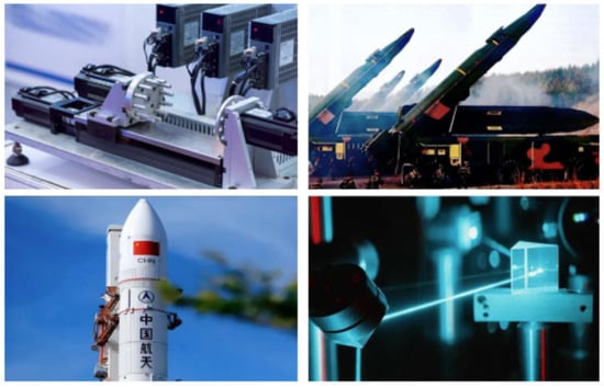
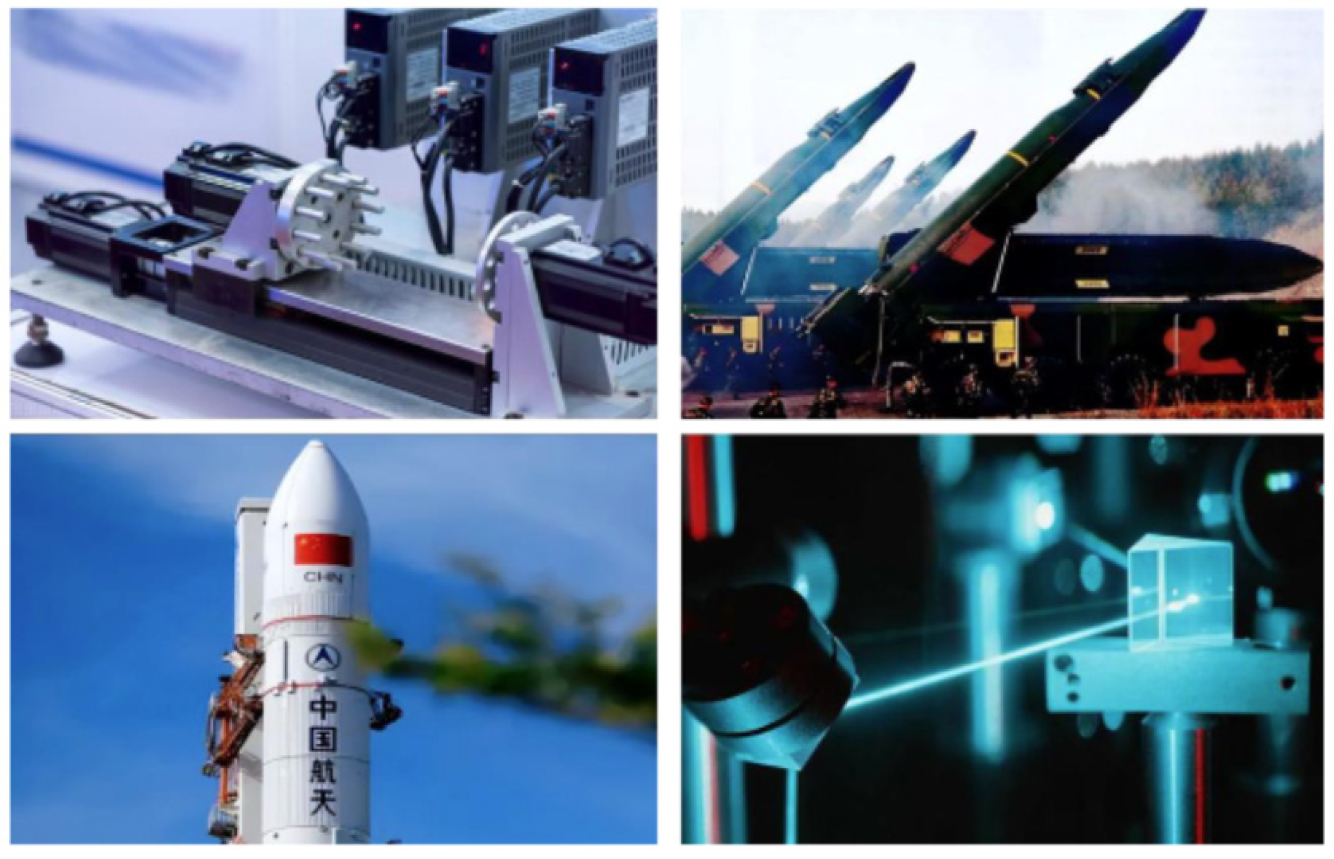
Monocrystalline silicon has significant characteristics such as a high refractive index, excellent light transmittance in the infrared band, and strong dimensional stability [17,18]. Curved optical lenses and mirrors made of monocrystalline silicon are widely used in national defense industrial equipment and large scientific devices such as infrared imaging and guidance systems, high-power laser cavity mirrors, and X-ray mirrors [7,19,20]. With the advancement of science and technology, ultra-precision cutting technology has developed rapidly and is widely used in high-precision product manufacturing, national defense and military, aerospace, optics, and laser fields. By cutting materials in the plastic domain, processing accuracy can be controlled within 10 nm [21]. Figure 1 showcases the key application scenarios of monocrystalline silicon in advanced manufacturing, aerospace, and defense-related fields.
Figure 1.
The applications of monocrystalline silicon [21].
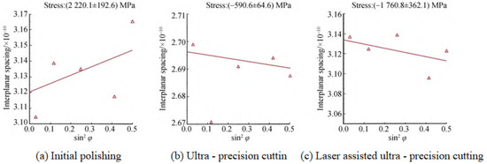
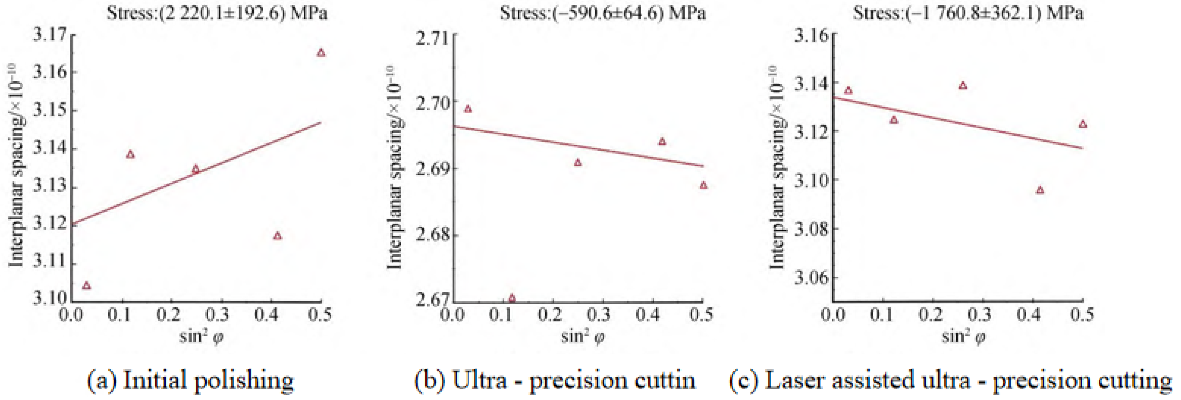
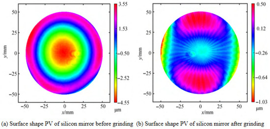
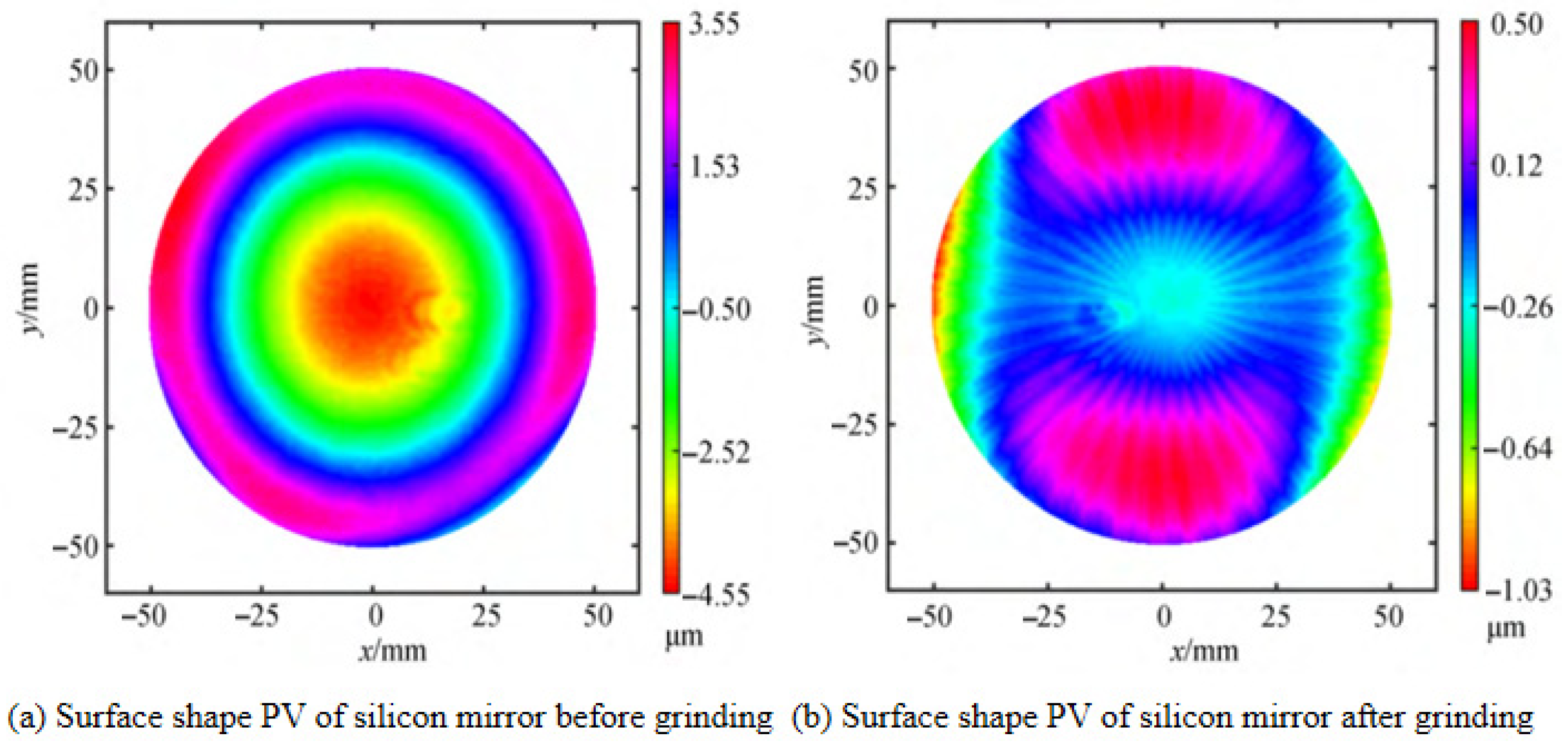
Chen Xiao [22] optimized the laser-assisted ultra-precision cutting process for monocrystalline silicon, using a Q-switched Nd:YAG laser (wavelength 1064 nm, power range 5–20 W) matched with a natural diamond tool (rake angle −15°, edge radius 50 nm). The cutting parameters were set as a feed rate of 3–8 μm/r, spindle speed of 2000 r/min, and laser focused spot diameter of 50 μm; the cutting zone temperature was monitored in real-time using an infrared thermometer (controlled at 200–300 °C to avoid lattice melting). After processing, surface shape accuracy was detected using a Zygo interferometer (resolution 0.1 nm), and subsurface damage was observed using a transmission electron microscope (TEM). By adjusting laser and cutting parameters, good surface shape control was achieved, with surface shape accuracy reaching 0.52 ± 0.03 μm (PV value, short for Peak-to-Valley, referring to the vertical distance between the highest and lowest points of a surface profile and a core indicator for evaluating optical component surface shape accuracy), effectively improving the surface shape quality of monocrystalline silicon optical components. Figure 2 shows the surface residual stress after initial polishing, ordinary ultra-precision cutting, and laser-assisted ultra-precision cutting, respectively. Yan J [23] found that during ultra-precision cutting of monocrystalline silicon, tool wear (micro-chipping and progressive wear) directly leads to decreased stability of cutting trajectories: when the cutting distance exceeds 8 km, feed error caused by tool wear increases the surface shape deviation (PV value) from the initial 0.3 μm to 0.8 μm, confirming the significant impact of tool wear on the surface shape accuracy of monocrystalline silicon optical components. Zhang Z [24] reviewed advanced high-precision material removal manufacturing technologies such as ultra-precision cutting, grinding, deterministic shape correction polishing, and ultra-smooth polishing. In terms of surface shape control for monocrystalline silicon optical components, the review noted that ultra-precision cutting can achieve nanoscale surface shape accuracy for monocrystalline silicon components; for example, by optimizing cutting parameters, surface shape errors can be controlled to less than 100 nm. Xie Lingbo [25] proposed a new pulsed ion beam (PIB) processing method. Experiments showed that the material removal resolution of PIB processing reaches 0.33 nm per 5 pulses. The use of the ant colony algorithm to optimize the processing trajectory reduced invalid paths by 57.7%. For monocrystalline silicon optical components with a 90 mm effective aperture, the surface shape accuracy was significantly improved to 0.552 nm after processing, opening a new path for surface shape control. Wang Ziguang [17] conducted research on ultra-precision grinding technology for monocrystalline silicon mirrors. They used ultra-fine grain diamond grinding wheels to process Φ100 mm × 5 mm monocrystalline silicon mirrors. The results showed that the surface roughness Ra of monocrystalline silicon was less than 10 nm, the subsurface damage depth was less than 100 nm, and the surface shape PV value was reduced from the initial 8.1 μm to 1.5 μm, achieving high-precision shape control. Figure 3 shows the comparison of surface shape PV values of silicon mirrors before and after grinding.
Figure 2.
Residual stress on the machined surface of single-crystal silicon [22].
Figure 3.
Comparison of surface shape Peak-to-Valley (PV) values of monocrystalline silicon mirrors before and after ultra-precision grinding [17].
2.2. Magnetorheological Polishing for Surface Shape Accuracy Control
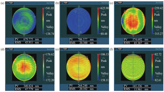
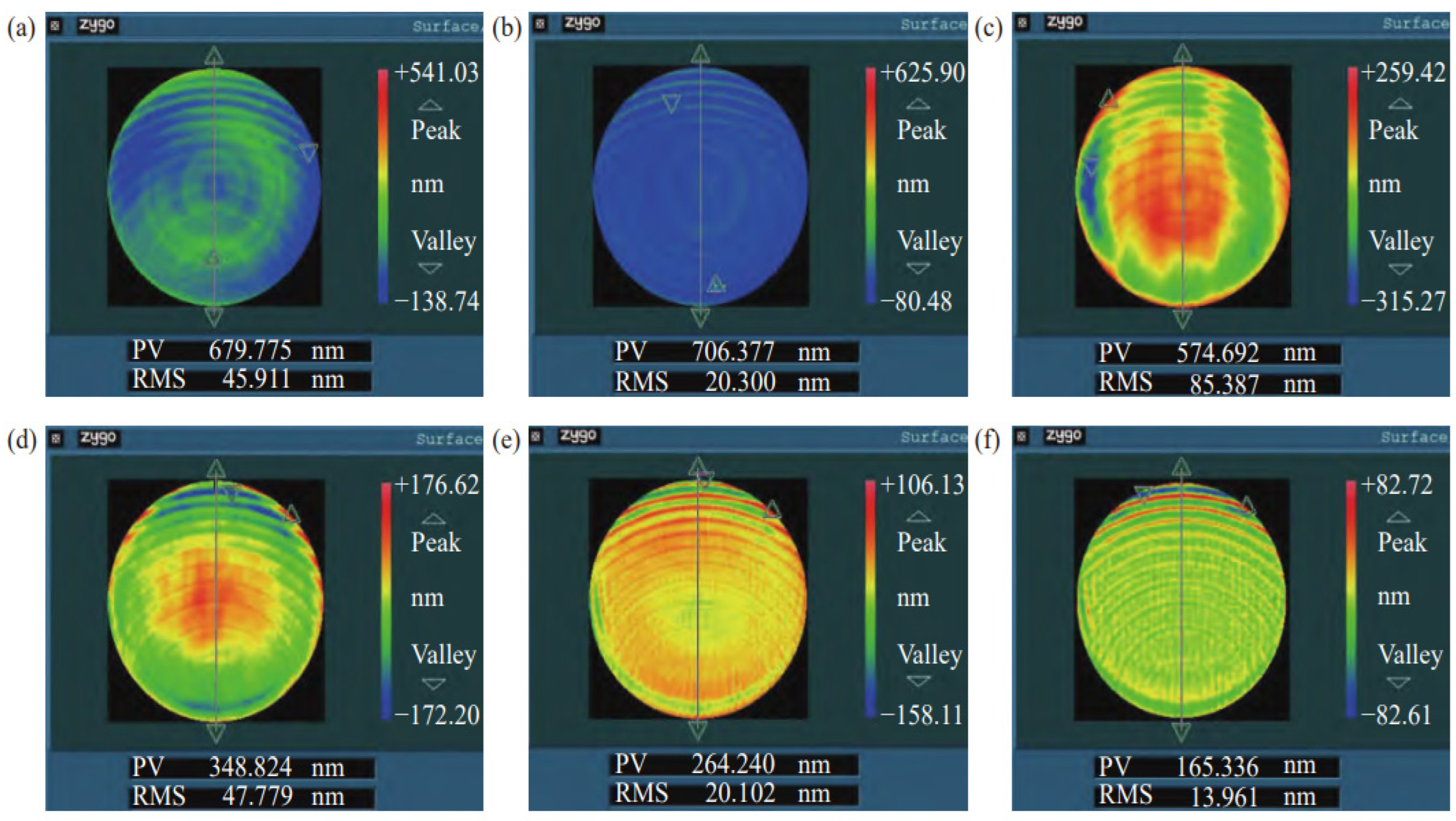
Magnetorheological polishing is an innovative, intelligent polishing technology integrating multiple fields, including flow dynamics, magnetic fields, mechanics, and tribology, spanning disciplines such as mechanical engineering, intelligent control, and electromagnetic materials [26]. During operation, the material removal function can be regulated by adjusting the control motor rotation speed, working gap, and magnetorheological polishing fluid flow rate [27]. Domestic research teams have explored shape control using this technology. Zhou Gang [28] proposed a composite processing technology combining magnetorheological polishing with pulsed ion beam processing. By dynamically adjusting the removal function, nanoscale surface shape control of monocrystalline silicon aspheric mirrors was achieved. Through active rotation of the magnetorheological removal function combined with ion beam shaping, the final surface shape accuracy of monocrystalline silicon components reached PV ≤ 0.836 μm (RMS ≤ 0.054 μm), enabling efficient shape correction. Khatri N [29] studied surface shape control of monocrystalline silicon in magnetorheological polishing. Through experimental and simulation analyses, the effects of parameters like magnetizing current, working gap, and rotation speed on surface shape accuracy were investigated, clarifying the correlation between each parameter and material removal uniformity to achieve effective convergence of surface shape errors. Kumar M [30] indicated that when applied to monocrystalline silicon optical components, magnetorheological polishing can control surface shape errors of planar components within λ/50 (RMS, λ = 632.8 nm) and achieve surface shape correction accuracy of λ/30 (RMS) for aspheric components. Manjesh K [31] reported that magnetorheological polishing for monocrystalline silicon optical components can achieve surface shape accuracy of PV ≤ 0.13 μm and RMS ≤ 0.012 μm. Gao Bo [32] conducted research on magnetorheological processing of monocrystalline silicon optical components. Uncertainty analysis of position and removal function errors revealed that both surface shape and mid-frequency errors had an uncertainty value of 3.5 nm. After processing, the RMS values of surface shape and mid-frequency errors were reduced to 20 nm and 14 nm, respectively, effectively enhancing surface shape accuracy. The process involved five iterations: four magnetorheological polishing steps and one smoothing process, as illustrated in Figure 4.
Figure 4.
Surface shape after actual machining. (a) Surface shape after the 1st magnetorheological polishing. (b) Surface shape after the 2nd magnetorheological polishing. (c) Surface shape after the smoothing process. (d) Surface shape after the 3rd magnetorheological polishing. (e) Surface shape after the 4th magnetorheological polishing. (f) Mid-frequency error distribution after the 4th magnetorheological polishing [32].
2.3. Laser Micromachining Technology for Surface Shape Accuracy Control
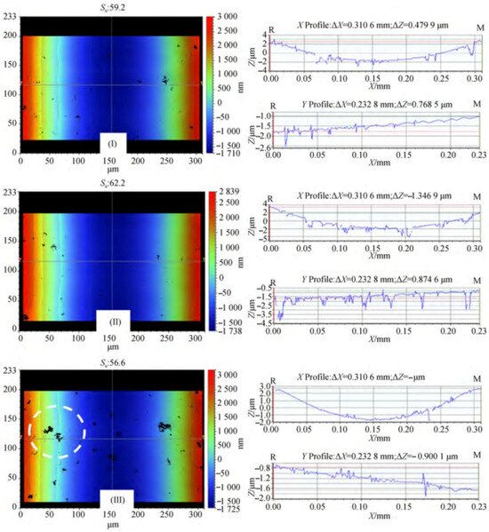
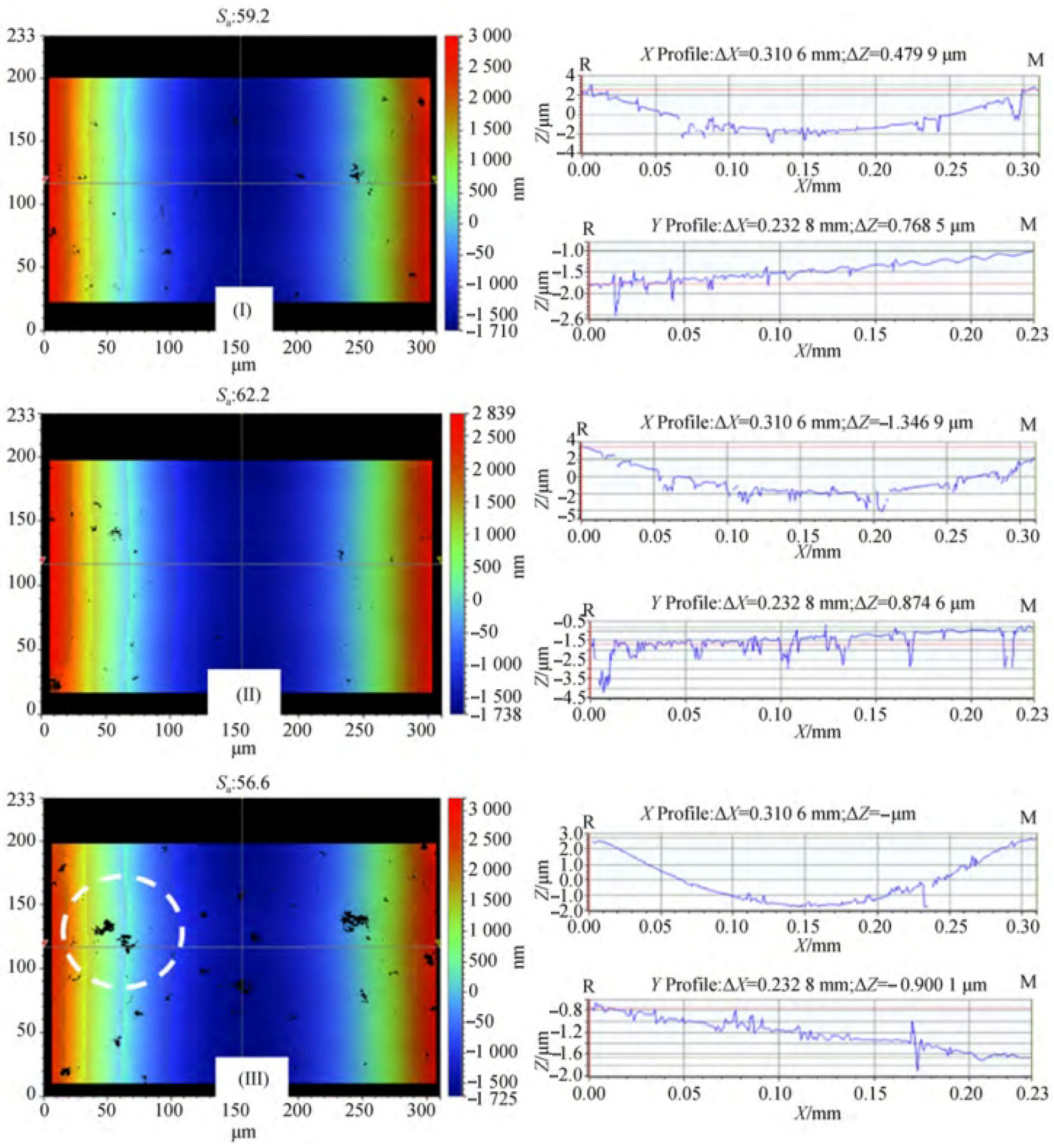
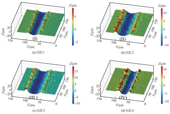
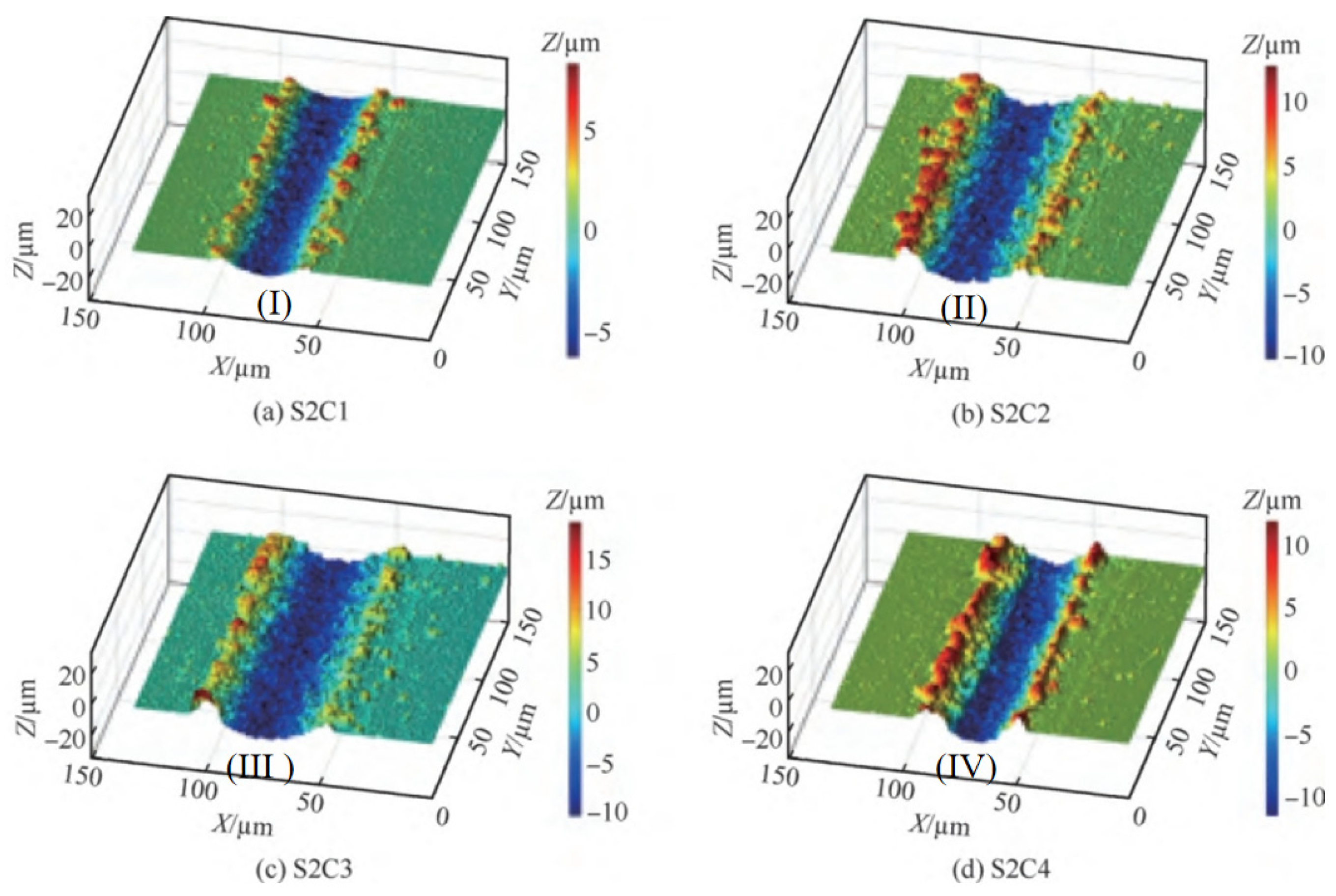
Laser processing technology has advantages such as strong adaptability to material types, no tool wear, and high processing accuracy, so its application in the processing field of hard and brittle materials is continuously expanding. With laser-induced methods, even micro-nano structures beyond the optical diffraction limit can be processed [33]. Domestic research teams have conducted studies on shape control using laser micromachining technology. Li Peizheng [34] adopted laser-assisted adaptive fly-cutting technology—based on the principle of “real-time topography detection-dynamic parameter adjustment”—to process micro-groove structures of monocrystalline silicon optical components. This technology uses a laser displacement sensor with a sampling frequency of 1 kHz to detect the workpiece surface profile online; after feeding data back to the numerical control system, it dynamically adjusts the tool feed rate to 5–15 μm/r and laser energy density to 10–30 J/cm2. A CO2 laser with a wavelength of 10.6 μm is employed to exert a thermal softening effect on monocrystalline silicon, which reduces material brittleness by over 40 and further reduces microcracks during cutting. On this basis, by further optimizing the tool trajectory through dynamic feed rate adjustment, precise control of the micro-groove surface shape accuracy was achieved: after processing, the verticality error of the micro-groove sidewall was ≤0.5°, the groove depth consistency error was controlled within ±3 μm, and the overall surface shape profile deviation (PV) was ≤5 μm. This effectively avoids surface shape distortion caused by brittle fracture and verifies the effectiveness of this technology in shape control of monocrystalline silicon microstructures. Figure 5 shows the roughness of micro-grooves cut by traditional fly-cutting at a feed rate of 8 mm/min under a segmented white light interferometer (The white dashed circle encloses the black spot-like brittle fracture and microcracks, and the blue curve is the actually measured surface profile curve of the sample). Huang W [35] conducted research on laser micro-polishing of monocrystalline silicon. The results showed that by controlling parameters such as laser energy density, the surface morphology of monocrystalline silicon can be effectively regulated. Under specific process conditions, the root mean square error (RMS) of the surface shape accuracy of monocrystalline silicon can be controlled within 1.2 nm. You Kaiyuan [36] conducted research on hard and brittle monocrystalline silicon. By systematically analyzing the laser-assisted nano-cutting process, relevant theories were constructed. The developed laser-assisted diamond turning system proposed a negative rake angle tool path generation and interference checking method, which improved the surface shape accuracy by 30% when processing monocrystalline silicon optical components. Yang Sishuo [37] conducted research on in situ laser-assisted turning repair of monocrystalline silicon. By optimizing laser power and turning parameters, precise repair of the surface shape of monocrystalline silicon optical components was achieved. Experiments showed that after repair, the surface shape accuracy PV value of the components decreased from the initial 2.1 μm to 0.58 μm, with a surface shape error repair rate of 72%. Zhang Quanli [38] showed that by adjusting the ultraviolet nanosecond laser power (5–20 W) and repetition frequency (10–50 kHz), the depth error of the processed grooves on the monocrystalline silicon surface can be controlled within ±0.8 μm, and combined with the width (10–30 μm) controlled with an accuracy of ±1.2 μm, precise creation of microstructure surface shapes was achieved, providing parameter references for improving the surface shape accuracy of optical components. Figure 6 shows the three-dimensional morphologies of monocrystalline silicon processed at different laser pulse repetition frequencies.
Figure 5.
Roughness of micro-grooves cut by traditional fly-cutting under a segmented white light interferometer at a feed rate of 8 mm/min [34].
Figure 6.
Three-dimensional morphologies of single-crystal silicon machined at different laser pulse repetition frequencies [38].
3. Nanoscale Precision Intrinsic Surface Property Control Generation Methods
During mechanical polishing of monocrystalline silicon surfaces, some common damage precursors are likely to be generated, such as absorbed impurities, cracks, and scratches. The specific types and distribution density of these damage precursors greatly affect the damage resistance of optical components. As a new category of surface and subsurface defects, nanoscale damage precursors can generally be divided into mechanical, pollution-related, and structural types. Studies on the processing methods for intrinsic surfaces of monocrystalline silicon show that technologies such as immersion polishing and ion beam processing can remove defects on the surface of optical components, obtain intrinsic surfaces with nanoscale precision, and thereby enhance the laser load-bearing capacity of monocrystalline silicon components.
3.1. Ion Beam Processing for Defect Removal
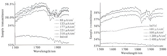
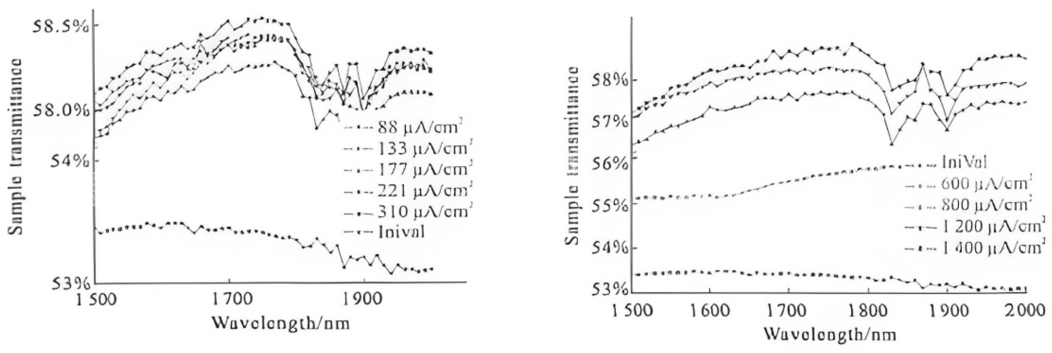
Ion beam polishing technology has many prominent features, such as good shape regularity and stability of the removal function, no edge effect, non-contact, non-destructive processing, and high processing accuracy, so it is often used as the final finishing process for high-precision optical parts [39]. Especially for microstructures with small feature sizes (<4 mm) and large local surface shape fluctuations (>2 μm/cm), ion beam polishing (IBF) offers more technical advantages than magnetorheological processing, which relies on large polishing wheels [40]. Domestic research teams have carried out relevant research on ion beam processing for defect removal. Shi Feng’s team [25] adopted an ultra-precision intelligent finishing strategy using pulsed ion beams for monocrystalline silicon optical components. By adjusting the ion beam energy density (50–80 eV) and pulse frequency, the surface microcrack density was reduced from 12/μm2 to 1.5/μm2, subsurface dangling bond defects were reduced by 78% ± 4%, and the damage layer depth was compressed from 2.3 μm to 0.2 μm, significantly reducing defects’ interference with optical performance. Chen Zhili, Liu Weiguo, et al. [41] conducted relevant research: when the ion beam energy was 1000 eV, the beam current density was 265 μA/cm2, and the sample was rotated and etched for 60 min, self-assembled dot structures formed on the (100) surface of monocrystalline silicon at different incident angles. When the angle increased from 0° to 25°, the roughness increased, the order of the dot structures was enhanced, and the average near-infrared transmittance was improved from 53% to over 57%, as shown in Figure 7, which presents the relationship between the sample’s transmittance and the etching beam current density as well as ion beam energy. Jiao Changjun, Li Shengyi, et al. from National University of Defense Technology [42] found that in ion beam processing of monocrystalline silicon optical mirrors, when the ion energy was 1200 eV and the beam current density was 220 μA/cm2, optimizing the pulse frequency and duty cycle reduced the surface microcrack density by 75%, and the subsurface damage layer depth from 1.8 μm to 0.3 μm, significantly enhancing the property control of the components. Qiao D, Shi F, et al. [43] found that with quantum dot sacrificial layers assisting pulsed ion beam sputtering of monocrystalline silicon, after processing, the surface microcrack density of monocrystalline silicon was reduced by 65%, and subsurface defects by 70%, effectively enhancing the property control of monocrystalline silicon optical components. Wanli Z, Feng S, et al. [44] found that in processing monocrystalline silicon optical components via ion beam sputtering and AMP technology, when ion energy was 1200 eV and beam current density 220 μA/cm2, the surface microcrack density was reduced by 75%, and subsurface damage layer depth decreased from 1.8 μm to 0.3 μm, effectively enhancing component property control. V.L.G and J.P.S [45] found that when using ion beams to modify monocrystalline silicon optical components, under specific parameters, the surface defect density of monocrystalline silicon can be reduced by approximately 60%, and the subsurface damage layer depth from 1.5 μm to 0.5 μm, effectively enhancing component property control and optimizing their optical performance.
Figure 7.
Relationship between the transmittance of monocrystalline silicon samples and etching beam current density, ion beam energy [41].
3.2. Plasma Etching for Defect Removal
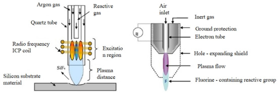
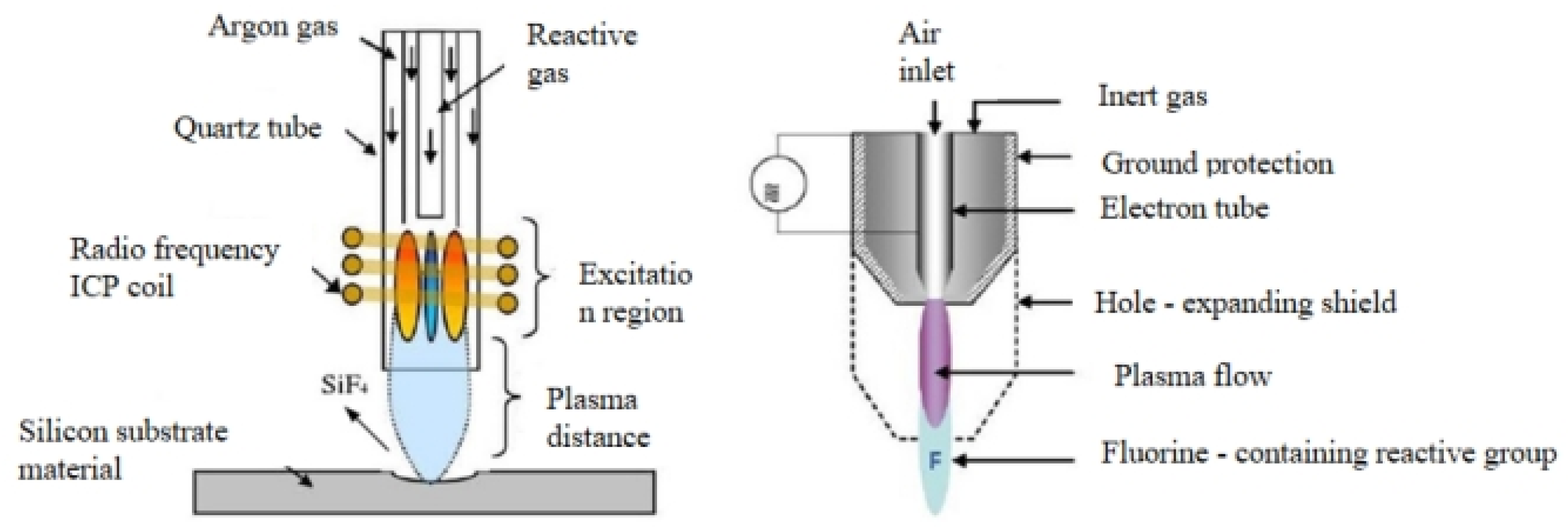
Plasma etching removes monocrystalline silicon defects via “physical bombardment-chemical reaction” synergy. Under a 13.56 MHz RF field, an Ar and CF4/O2 mixture becomes plasma. High-energy Ar+ bombards to break Si-Si bonds; F combines with Si to form volatile SiF4 for atomic-level removal. Adjusting pressure (10–50 Pa), gas ratio (CF4/O2 = 5:1–2:1), and RF power (300–800 W) enables control of etching rate (10–100 nm/min) and surface roughness, fitting for removing its microcracks and impurities. With the deepening of researchers’ exploration of plasma physics, many unique properties of plasma have been gradually revealed. At the same time, the processing of optical components is moving towards large aperture, non-destructive, and ultra-smooth directions. In this context, plasma processing technology has gradually been applied in the optical processing field. Among them, the successful development of non-contact polishing methods such as neutral ion beam polishing and plasma-assisted chemical polishing is the most representative [46,47]. Domestic research teams have conducted studies on plasma etching for defect removal. Li Kun [48] found in research that when radical plasma etches monocrystalline silicon optical components, under the conditions of a microwave power of 400 W, working pressure of 20 Pa, and CF4/O2 flow ratio of 5:1, the surface defect density was reduced by 68%, and the subsurface damage layer depth was reduced to 0.4 μm, effectively improving the property control of components. The working principle of plasma is shown in Figure 8.
Figure 8.
Working principle of plasma [48].
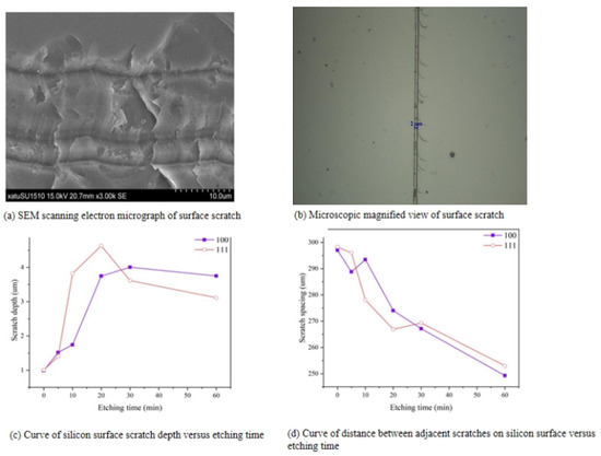
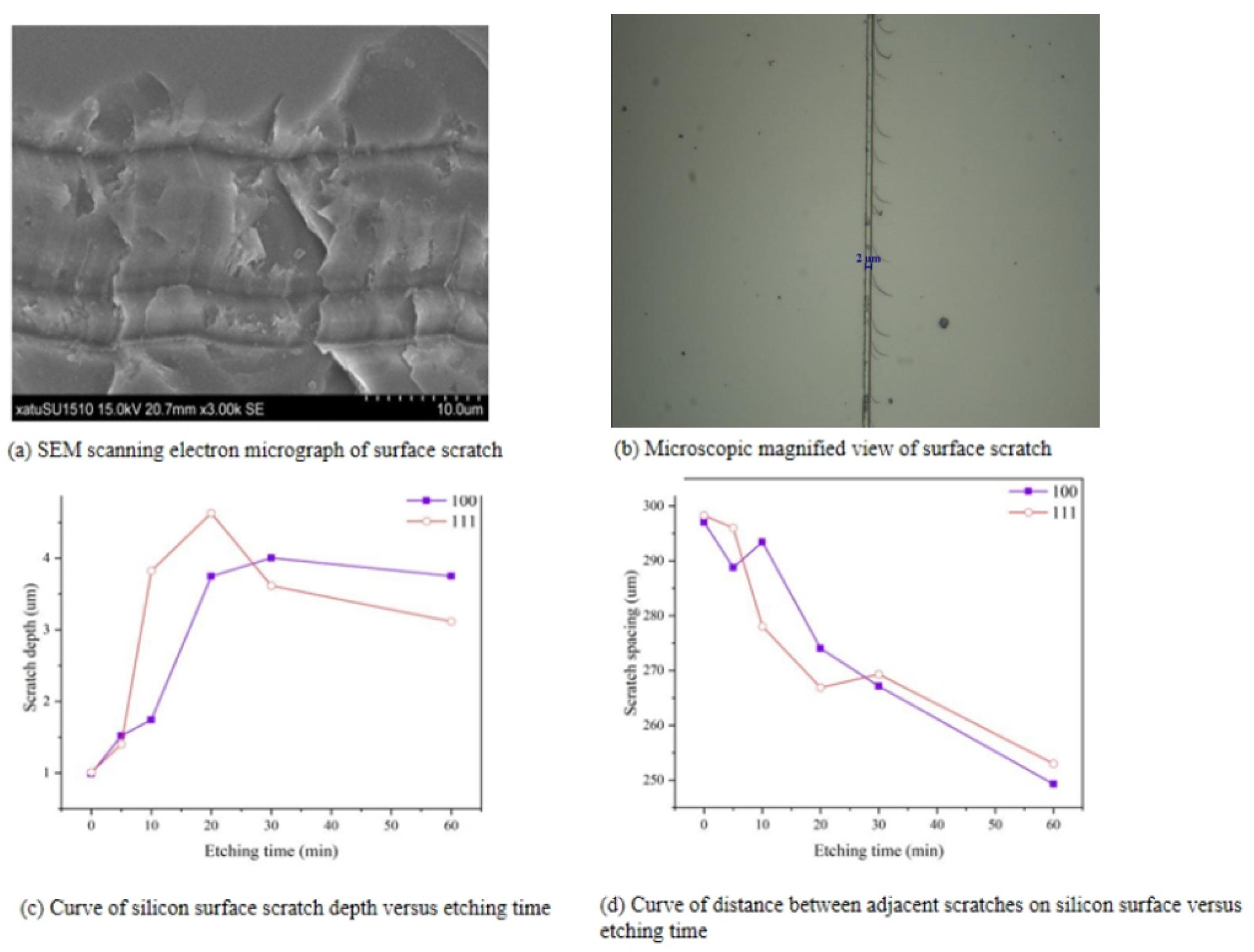
Zhidong F, Yi Z, et al. [49] proposed an ultra-precision polishing method based on plasma-induced atomic selective etching effect (PASE). For 2-inch monocrystalline silicon wafers, the surface Sa roughness was reduced from 195 nm to below 1 nm within 5 min, and TEM observation confirmed no subsurface damage, significantly reducing surface and subsurface defects. Bing W [50] conducted research and found that in an atmospheric inductively coupled plasma, the etching mode can be adjusted by changing the ratio of CF4/O2 reaction gases. When the CF4/O2 ratio is higher than 2:1, atomic selective etching is achieved, which can reduce the surface Sa roughness of monocrystalline silicon to 0.14 nm, effectively reducing surface defects and improving the property control of monocrystalline silicon optical components. Zhiping Z [51] found that in the processing of monocrystalline silicon photonic devices, by combining electron beam lithography and ICP etching, after optimizing the Cl2/C4F8 gas ratio, the sidewall roughness of silicon waveguides was reduced from 40 nm to below 10 nm, and the optical loss was reduced by 30%, effectively reducing defects. Marchack N [52] conducted research on monocrystalline silicon optical components. By optimizing the plasma etching chemical process and adjusting the CF4:CHF3 ratio, in the hard mask opening step of monocrystalline silicon waveguides, the line edge roughness (LER) of isolated waveguides could be reduced by 26–43% compared with the initial lithography value, with the minimum reaching 2.5 nm. Song Zirong [53] found that when using radical plasma to process monocrystalline silicon optical components, microwave power and fluorine-containing gas flow have a significant impact on the etching rate. When the processing time reaches 60 min, this method can reduce the depth of scratches on the monocrystalline silicon surface. Measured by a contact profilometer, the scratch depth was 1 μm. The morphology characteristics of scratches on the silicon surface were observed by SEM, as shown in Figure 9a; under a 1000× optical microscope, the width of a single scratch was measured to be 2 μm. Figure 9b,c is the curve of scratch depth on the monocrystalline silicon surface with different etching times measured by a contact profilometer, and Figure 9d is the curve of scratch spacing on the silicon surface with different etching times recorded by a contact profilometer.
Figure 9.
Multidimensional characterization of surface scratch characteristics and evolution law during the etching process of single-crystal silicon optical components [53].
3.3. Chemical–Mechanical Polishing for Defect Removal
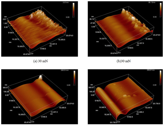
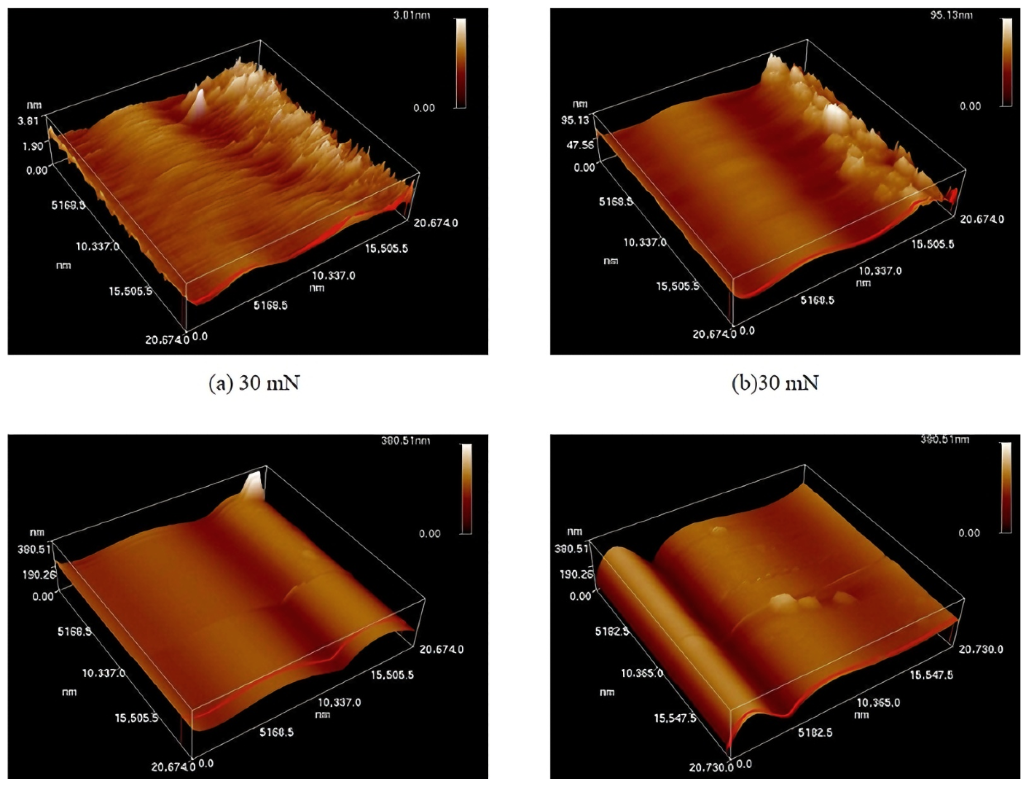
During chemical–mechanical polishing, due to the anisotropic characteristics of monocrystalline silicon materials, the evolution law of defects such as surface scratches is relatively complex [54,55,56,57,58]. Researchers at home and abroad have carried out a lot of relevant explorations on the defect problems in chemical–mechanical polishing. Xia Jingjing [59] conducted research on the evolution of scratches in chemical–mechanical polishing of monocrystalline silicon, clarified the variation law of the number and length of scratches with process parameters during polishing, and effectively reduced the performance defects of monocrystalline silicon optical components caused by scratches. Jiang B [60] studied the chemical–mechanical polishing process of silicon mirrors. By establishing an edge effect model and optimizing process parameters, micro-nano scale roughness control was achieved, with surface roughness RMS < 0.5 nm, and surface scratches and subsurface damage were effectively reduced, significantly improving the performance of monocrystalline silicon optical components. Jingjing X [61] constructed a microscale material removal model to study chemical–mechanical polishing of monocrystalline silicon. Experiments showed that when the impurity particle concentration was 0.00100%, there were few scratches on the monocrystalline silicon surface and they were easy to identify; when it increased to 0.00200%, scratches on the Si(111) surface overlapped with each other. Hou Baojiang [62] conducted chemical–mechanical polishing experiments on monocrystalline silicon wafers using a commercial polishing machine. It was found that when the rotation speed of the polishing pad and polishing head increased from 30 rpm to 60 rpm, the polishing load increased from 20 N to 50 N, the surface roughness was reduced from 52 nm to 18 nm, and the total thickness variation was reduced by 35%. Xing Y [63] synthesized silica sol using organic amine catalysis for monocrystalline silicon polishing fluid. Experiments showed that this sol reduced the number of microcracks on the monocrystalline silicon surface from 15/mm2 to less than 3/mm2, the subsurface damage depth from 45 nm to 12 nm, and the corrosion pit density by 80%. Chen Xiaochun [64] studied monocrystalline silicon optical components through a series of chemical–mechanical polishing tests. A mathematical model was established, showing that when the polishing pressure is 20–30 kPa and the rotation speed is 60–80 rpm, the material removal rate can reach 0.8–1.2 μm/h, which can effectively remove the damage layer, and the subsurface damage depth can be controlled within 20 nm, reducing defects caused by damage and ensuring component performance. Figure 10 shows the surface morphologies of monocrystalline silicon wafers under water lubrication conditions with polishing forces of 30 mN, 50 mN, 70 mN, and 90 mN while maintaining a sliding speed of 8.00 mm·s−1. Table 1 summarize the data on the displacement of the monocrystalline silicon substrate and subsurface damage depth obtained from simulations. The simulation results demonstrate that an increase in grinding depth significantly augments the damage thickness of the monocrystalline silicon substrate. Notably, after the amorphous SiO2 oxide layer is completely removed, the monocrystalline silicon substrate is directly subjected to the mechanical action of abrasive grains. This results in a significant increase in the surface damage thickness of the monocrystalline silicon.
Figure 10.
Surface morphology diagrams of wear scars of single-crystal silicon wafers under water-lubricated conditions with different polishing forces [64].
Table 1.
Displacement of monocrystalline silicon substrate and subsurface damage depth at a grinding distance of 9 nm [65].
4. Combined Processes for Nanoscale Precision Shape and Property Control
To achieve precise control of the shape and performance of nanoscale precision surfaces, based on in-depth research on various processing technologies, a set of high-precision, low-defect combined processes has been developed. Different from the traditional processing mode, where various processes are simply connected and converted, this combined process reasonably distributes the achievement of all indicators throughout the process flow, thereby realizing the controllable manufacturing of monocrystalline silicon components with high precision and low defects in terms of shape and performance.
4.1. Classification and Explanation of Nanoscale Shape and Property Control Processes for Monocrystalline Silicon
To systematically clarify the diversity of nanoscale shape control processes for monocrystalline silicon and their technical characteristics, this section classifies the processes based on the machining energy form and material interaction mechanism. Table 2 presents the classification of key shape control processes, including their typical implementations, core principles, and application scenarios, aiming to provide a clear framework for understanding the applicability and advantages of each process type.
Table 2.
Simplified classification of shape control processes.
4.2. Synergistic Process of Ultra-Precision Cutting Preforming and Magnetorheological Polishing Finishing
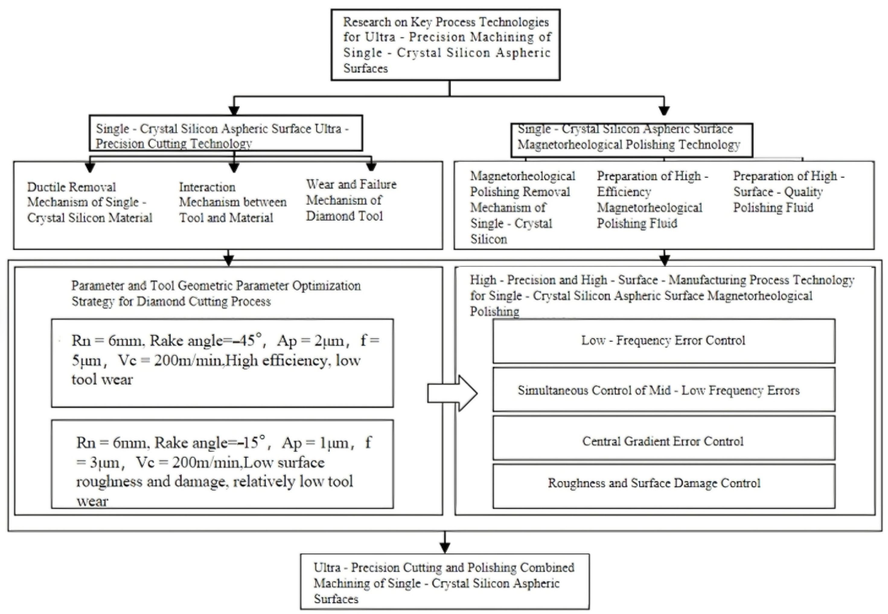
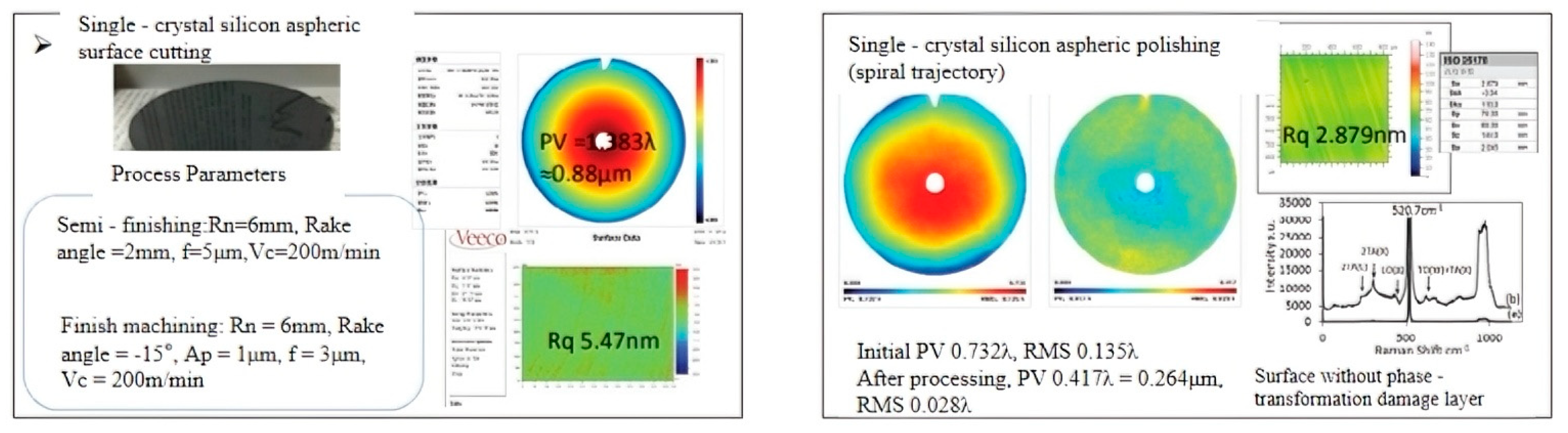
Combining magnetorheological polishing with ultra-precision cutting can not only make up for the efficiency shortage of magnetorheological polishing in aspheric processing but also eliminate the tool marks remaining on the surface of monocrystalline silicon after diamond cutting, effectively remove surface brittle cracks, reduce damage to the processed surface of monocrystalline silicon, and thus improve processing accuracy and surface roughness. Xu Feifei [66] adopted the combined process of ultra-precision cutting and magnetorheological polishing in the research on ultra-precision processing of monocrystalline silicon aspheric surfaces. Through parameter optimization, ultra-precision cutting can achieve surface shape accuracy with a PV value of 1–5 μm. Subsequent magnetorheological polishing can eliminate residual cutting tool marks, significantly reduce the surface roughness from the high value after cutting to below Ra 3 nm, and improve component quality. Figure 11 shows the combined processing method of diamond cutting and magnetorheological polishing for monocrystalline silicon aspheric surfaces, which has been verified by experiments, and the processing results are shown in Figure 12.
Figure 11.
Combined machining process method of diamond cutting and magnetorheological polishing for single-crystal silicon aspheric surfaces [66].
Figure 12.
Combined machining results of diamond cutting and magnetorheological polishing for single-crystal silicon aspheric surfaces [66].
Khatri N [29] conducted research aiming to achieve nanoscale surface generation of monocrystalline silicon using magnetorheological polishing. Through experimental exploration, under optimized process parameters, the surface roughness of monocrystalline silicon was significantly reduced from the initial high value to 6.4 nm. In terms of shape control, this process can effectively improve the surface microstructure, laying a good foundation for subsequent ultra-precision optical component processing. Niu Y [67] conducted research on monocrystalline silicon parabolic mirrors. Through ultra-precision grinding process experiments, in the processing of 195 mm diameter monocrystalline silicon parabolic mirrors, the surface shape accuracy peak–valley value was improved from 21.4 μm to 3.77 μm, and the roughness Rms value was improved from 0.625 μm to 0.11 μm, effectively improving the shape control accuracy of monocrystalline silicon optical components. Hongfei T [68] explored the ultra-precision grinding process of monocrystalline silicon wafers. The study found that grinding parameters significantly affect plastic deformation and subsurface damage. Under optimized parameters, the subsurface damage depth can be controlled within 50 nm, and the surface shape accuracy peak–valley value can reach 0.8 μm. Hongfei T deeply explored the mechanism of ultra-precision grinding of monocrystalline silicon wafers. A three-dimensional microstructure model was established to reveal the material removal law. Under optimized process parameters, the surface roughness Rz value of monocrystalline silicon wafers after grinding was as low as 10 nm, and the surface shape accuracy peak-valley value could reach 0.5 μm, providing key references for the application of ultra-precision grinding technology in the manufacturing of monocrystalline silicon optical components.
4.3. Case Study on High-Precision, Low-Defect Processing of Cylindrical Components
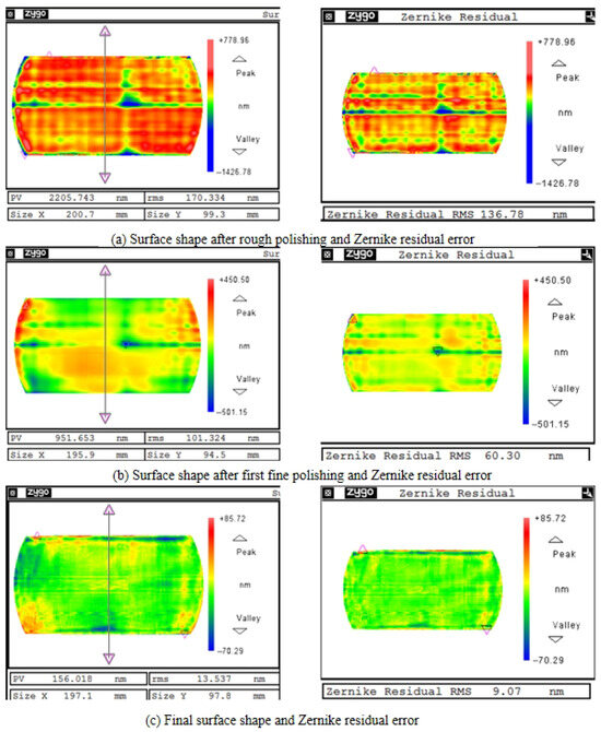
With the rapid advancement of science and technology, aspheric cylindrical mirrors are not only widely used in scanning systems in civil fields such as graphic and barcode scanning, digital fax equipment, medical instruments, and photographic equipment [69] but also play a key role in high-end military and aerospace fields such as laser transmitters [70], high-power laser resonator lenses [71], long-distance information transmission systems [72], satellite navigation systems [73], and periscopes [74]. Domestic research teams have carried out relevant explorations on high-precision, low-defect processing of cylindrical components. Zhao Shuang [75] adopted a combination of classical and modern processes to process a monocrystalline silicon plano-concave cylindrical mirror with dimensions of 300 × 150 × 50 mm and a radius of 4000 mm. Detected by a profilometer and interferometer, the actual radius after processing was 4028 mm, the surface shape error P-V value reached 0.15 μm, and the finish was grade III, successfully achieving high-precision shape control. Zhang Changda [76] proposed using silicon instead of low-refractive index quartz substrates to improve the numerical aperture of microlenses and preparation efficiency. Taking a silicon-based aspheric cylindrical microlens array with a numerical aperture of 2.9 as an example, through mask moving exposure, multiple glue-coating cycle exposure, and plasma etching, the prepared microlens array achieved a surface shape accuracy PV of 0.766 μm and a surface roughness Ra of 3.4 nm, realizing precise shape control. Jie L [77] conducted research on ultra-precision grinding of monocrystalline silicon cylindrical mirrors. Through optimizing process parameters and using advanced grinding equipment and methods, high-precision shape control was achieved. After grinding, the surface shape accuracy PV value of the cylindrical mirror reached 0.08 μm, the cylindricity error was controlled within 0.05 μm, and the surface roughness Ra was as low as 0.2 nm, effectively improving the optical performance and quality of monocrystalline silicon cylindrical mirrors. Zhang W [78] conducted research on the combined surface modification of monocrystalline silicon cylindrical mirrors. Through process optimization, precise shape control was achieved, with the surface shape accuracy PV value reaching 0.09 μm and the surface roughness Ra reduced to 0.25 nm, effectively improving optical performance, providing a new method for the shape and property control process of monocrystalline silicon optical components, and facilitating their application in optical systems. Tian Ye [79] developed a combined shape and property control process for the manufacturing of monocrystalline silicon mirrors. Through optimizing processing parameters, the surface shape accuracy PV value was better than 0.1 μm, and the surface roughness Ra was as low as 0.3 nm, effectively reducing the density of surface and subsurface defects, providing strong support for the application of monocrystalline silicon optical components in high-precision optical systems. Figure 13 shows the convergence process of the surface shape accuracy of a 200 mm convex cylindrical mirror. Table 3 shows that after machining, the actual radius is 4028 mm, the surface shape error (PV value) is 0.15 μm, the cylindrical accuracy is 0.1 μm, and the surface finish is Grade III.
Figure 13.
Convergence process of surface shape accuracy of 200 mm convex cylindrical mirror [79].
Table 3.
Machining results [75].
5. Conclusions
Monocrystalline silicon optical components are indispensable in high-energy lasers, infrared guidance, and other fields due to their high refractive index, high dimensional stability, and excellent infrared performance. Their nanoscale shape and property control manufacturing is the core to improving system performance. Based on existing research, the following conclusions are drawn:
Shape control technologies have achieved precision breakthroughs through multi-method collaboration. Ultra-precision cutting can achieve nanoscale surface shape accuracy through parameter optimization, for example, the PV value reaches 0.52 μm after laser-assisted cutting, but it is significantly affected by tool wear, with the surface shape deviation increasing to 0.8 μm after 8 km cutting; magnetorheological polishing can control the planar surface shape error within λ/50 (RMS, λ = 632.8 nm), and the PV value is as low as 0.13 μm after combining with ion beam shaping; laser micromachining can precisely control microstructures, such as micro-groove deviation ≤ 5 μm, and surface shape RMS ≤ 1.2 nm under specific processes. For structures such as cylindrical surfaces, combined processes (e.g., ultra-precision cutting + magnetorheological finishing) achieve high precision with PV 0.08 μm and cylindricity 0.05 μm.
Property control technologies focus on defect suppression and performance improvement. Ion beam processing reduces the microcrack density from 12/μm2 to 1.5/μm2, compresses the damage layer from 2.3 μm to 0.2 μm, and increases the near-infrared transmittance to over 57%; plasma etching reduces the roughness from 195 nm to below 1 nm within 5 min, with Sa reaching 0.14 nm under specific parameters; chemical–mechanical polishing reduces the number of microcracks from 15/mm2 to less than 3/mm2, and the corrosion pit density is reduced by 80%.
Combined processes break through the limitations of single processes, taking into account both precision and defect control. The current core issues include the following: there is still a contradiction between precision control and processing efficiency for complex structures; the quantitative characterization and control mechanism of nanoscale defects are not fully clarified; the intelligence level of multi-process collaboration is insufficient; parameter matching relies on experience accumulation. In the future, it is necessary to focus on developing data-driven intelligent processing systems, cross-scale in situ defect detection technologies, and new composite energy field processing technologies to lay the foundation for achieving the manufacturing goal of “ultra-high precision, ultra-low defects” for monocrystalline silicon components. On the premise of ensuring machining performance, efforts will be made to develop degradable machining media and low-energy-consumption machining equipment, and explore new modes such as “dry machining” and “near-zero-emission machining”, so as to reduce the environmental impact of nanoscale machining of monocrystalline silicon and contribute to the low-carbon transition of the manufacturing industry.
Author Contributions
S.Q.: Investigation, Data curation, Formal analysis, and Writing—original draft. Z.W.: Investigation and Writing—original draft. Z.H.: Data curation and Formal analysis. B.Z.: Investigation and Data curation. X.X.: Resources and Supervision. All authors have read and agreed to the published version of the manuscript.
Funding
This study was financially supported by the National Natural Science Foundation of China (62575308, 62375019), and the China Postdoctoral Science Foundation under Grant Number 2024M764130.
Data Availability Statement
The original contributions presented in this study are included in the article.
Conflicts of Interest
The authors declare that they have no known competing financial interests or personal relationships that could have appeared to influence the work reported in this paper.
References
- Hecht, J. Beam Weapons: The Next Arms Race; Plenum Press: New York, NY, USA, 1984. [Google Scholar]
- Seidel, R.W. From glow to flow: A history of military laser research and development. Hist. Stud. Phys. Biol. Sci. 1987, 18, 111–147. [Google Scholar] [CrossRef] [Scilit]
- Hecht, J. Beam: The race to make the laser. Opt. Photonics News 2005, 16, 24–29. [Google Scholar] [CrossRef] [Scilit]
- He, Q.; Zong, S. Development progress and thinking of shipborne laser weapons. Laser Infrared 2017, 47, 1455–1460. [Google Scholar]
- Ren, G.G.; Yi, W.W.; Qi, Y. U.S. theater and strategic UVA-borne laser weapon. Laser Optoelectron. Prog. 2017, 54, 100002. [Google Scholar]
- Cui, Y.; He, H.B.; Fan, Z.X. Development of high energy laser weapon and research of laser protective coatings. Laser Optoelectron. Prog. 2006, 43, 10–13. [Google Scholar]
- Song, C.; Tian, Y.; Shi, F.; Zhang, K.; Shen, Y. Optimization of ion beam inclined incidence processing parameters for monocrystalline silicon cylindrical mirrors. Acta Opt. Sin. 2020, 40, 167–177. [Google Scholar]
- Zegrya, A.G.; Sokolov, V.V.; Zegrya, G.G. The effect of the doping level of starting silicon single crystals on structural parameters of porous silicon produced by electrochemical etching. Tech. Phys. Lett. 2019, 45, 1067–1070. [Google Scholar] [CrossRef] [Scilit]
- Tian, Y.; Shi, F.; Dai, Y.F. Laser absorption precursor research: Microstructures in the subsurface of mono-crystalline silicon substrate. Appl. Opt. 2017, 56, 8507–8516. [Google Scholar] [CrossRef] [Scilit] [PubMed]
- Tian, Y.; Dai, Y.; Shi, F. Correlation between laser energy absorption coefficient and substrate surface quality of monocrystalline silicon mirrors. J. Natl. Univ. Def. Technol. 2015, 37, 26–29. [Google Scholar]
- Wang, P.; Wang, B.; Melkote, S.N. Modeling and simulation of phase transformation and crack formation during scribing of mono-crystalline silicon. Int. J. Mech. Sci. 2020, 175, 105527. [Google Scholar] [CrossRef] [Scilit]
- Zhang, X.; Huang, T.; Xiao, R. Behavior characteristics of monocrystalline silicon with different crystal planes under femtosecond laser action. Chin. J. Lasers 2017, 44, 0102012. [Google Scholar] [CrossRef] [Scilit]
- Zhu, Y.; Li, X.; Wang, Z. Prediction of subsurface damage in fixed abrasive grinding of optical hard and brittle materials. Opt. Precis. Eng. 2017, 25, 367–374. [Google Scholar]
- Cooke, F.; Brown, N.; Prochonow, E. Annual lapping of precision optical flatware. Opt. Eng. 1976, 15, 407–415. [Google Scholar] [CrossRef] [Scilit]
- Li, S.; Peng, X. Theoretical basis and methods of controllable flexible manufacturing for optical parts. J. Mech. Eng. 2013, 49, 1–9. [Google Scholar] [CrossRef] [Scilit]
- Wang, Y.; Sun, Y.; Mo, H. Research on milling parameters optimization of monocrystalline silicon lenses. Aeronaut. Manuf. Technol. 2021, 64, 90–94. [Google Scholar]
- Wang, Z.; Zhou, P.; Gao, s.; Dong, Z. Ultra-precision grinding process of monocrystalline silicon mirrors. Opt. Precis. Eng. 2019, 27, 1087–1095. [Google Scholar] [CrossRef] [Scilit]
- Liu, K.; Li, L. Review of air-to-air missiles and infrared guidance system development. Laser Infrared 2016, 46, 5–10. [Google Scholar]
- Li, M.; Wu, J.; Wu, Y. Current status and development of X-ray mirror development technology. Opto-Electron. Eng. 2020, 47, 62–73. [Google Scholar]
- Cui, J. Research on Micro-Nano Scale Ultra-Precision Cutting Characteristics of Monocrystalline Silicon. Ph.D. Thesis, Kunming University of Science and Technology, Kunming, China, 2024. [Google Scholar]
- Fang, F.Z.; Lai, M.; Wang, J.S. Nanometric cutting: Mechanisms, practices and future perspectives. Int. J. Mach. Tools Manuf. 2022, 178, 103–105. [Google Scholar] [CrossRef] [Scilit]
- Chen, X.; Ke, J.; She, Z. Optimization of laser-assisted ultra-precision cutting process and surface characteristics of monocrystalline silicon. Opt. Precis. Eng. 2023, 31, 99–108. [Google Scholar] [CrossRef] [Scilit]
- Yan, J.; Syoji, K.; Tamaki, J. Some observations on the wear of diamond tools in ultra-precision cutting of single-crystal silicon. Wear 2003, 255, 1380–1387. [Google Scholar] [CrossRef] [Scilit]
- Zhang, Z.; Yan, J.; Kuriyagawa, T. Manufacturing technologies toward extreme precision. Int. J. Extrem. Manuf. 2019, 1, 022001. [Google Scholar] [CrossRef] [Scilit]
- Xie, L.; Shi, F.; Tian, Y. Ultra-precision intelligent shaping strategy of optical components by pulsed ion beam (cover article · invited). Infrared Laser Eng. 2024, 53, 50–64. [Google Scholar]
- Dong, G.; Hu, H.; Li, S. Design and optimization of small-aperture magnetorheological polishing device based on permanent magnets. Nanotechnol. Precis. Eng. 2015, 13, 251–257. [Google Scholar] [CrossRef]
- Li, S. Analysis of Magnetorheological Polishing Removal Mechanism and Performance Optimization. Ph.D. Thesis, Shandong University of Science and Technology, Qingdao, China, 2019. [Google Scholar] [CrossRef]
- Zhou, G.; Guo, S.; Shi, F. Aspheric nanoscale precision controllable flexible manufacturing technology. Sci. China Technol. Sci. 2023, 53, 1337–1350. [Google Scholar]
- Khatri, N.; Tewary, S.; Manoj, J.X.; Garg, H.; Karar, V. Magnetorheological finishing of silicon for nanometric surface generation: An experimental and simulation study. J. Intell. Mater. Syst. Struct. 2018, 29, 2456–2464. [Google Scholar] [CrossRef] [Scilit]
- Kumar, M.; Kumar, A.; Alok, A. Magnetorheological method applied to optics polishing: A review. IOP Conf. Ser. Mater. Sci. Eng. 2020, 804, 012012. [Google Scholar] [CrossRef] [Scilit]
- Manjesh, K.; Narayan, H.Y.S.; Abhinav, K. An overview of magnetorheological polishing fluid applied in nano-finishing of components. J. Micromanuf. 2022, 5, 82–100. [Google Scholar]
- Gao, B.; Fan, B.; Wang, J. Process method for uncertainty error in magnetorheological processing of optical components. Infrared Laser Eng. 2024, 53, 211–220. [Google Scholar]
- Feng, Z.; Cheng, K.; Cao, K. Laser-induced periodic nano-structure patterns and coloring on free-form surfaces. Laser Optoelectron. Prog. 2020, 57, 111423. [Google Scholar] [CrossRef] [Scilit]
- Li, P.; Du, X.; Sun, Z. Efficient adaptive fly-cutting of infrared optical microstructure surfaces. Opt. Precis. Eng. 2022, 30, 1845–1856. [Google Scholar] [CrossRef] [Scilit]
- Huang, W.; Li, T.; Long, G. Surface topography and subsurface structure evolution in laser micro polishing of monocrystalline silicon. Opt. Laser Technol. 2024, 177, 111068. [Google Scholar] [CrossRef] [Scilit]
- You, K. Basic Research on Laser-Assisted Ultra-Precision Cutting of Hard and Brittle Materials. Ph.D. Thesis, Tianjin University, Tianjin, China, 2022. [Google Scholar] [CrossRef]
- Yang, S.; Huang, W.; Zhang, J. In-situ laser-assisted turning repair of monocrystalline silicon. China Surf. Eng. 2025, 1–10. Available online: http://kns.cnki.net/kcms/detail/11.3905.TG.20250416.1358.010.html (accessed on 20 November 2025).
- Zhang, Q.; Chu, C.; Zhai, J. Mechanism of surface feature creation in ultraviolet nanosecond pulsed laser ablation of monocrystalline silicon. Acta Aeronaut. Astronaut. Sin. 2022, 43, 515–527. [Google Scholar]
- Wang, T.; Ke, X.; Huang, L. Computer-controlled finishing via dynamically constraint position-velocity-time scheduler. J. Manuf. Process. 2023, 87, 97–105. [Google Scholar] [CrossRef] [Scilit]
- Wan, S.; Wei, C.; Hu, C. Novel magic angle-step state and mechanism for restraining the path ripple of magnetorheological finishing. Int. J. Mach. Tools Manuf. 2021, 161, 103673. [Google Scholar] [CrossRef] [Scilit]
- Chen, Z.; Liu, W. Nanostructures and optical properties of monocrystalline silicon induced by different ion beam parameters. Infrared Laser Eng. 2013, 42, 2490–2495. [Google Scholar]
- Jiao, C.; Li, S.; Xie, X. Process controllability analysis of ion beam processing removal function for optical mirrors. Opt. Tech. 2008, 5, 651–654. [Google Scholar]
- Qiao, D.; Shi, F.; Tian, Y. Ultra-smooth polishing of single-crystal silicon carbide by pulsed-ion-beam sputtering of quantum-dot sacrificial layers. Materials 2023, 17, 157. [Google Scholar] [CrossRef] [Scilit]
- Wanli, Z.; Feng, S.; Ci, S. Study on damage characteristics of fused silica under ion beam sputtering and AMP technique. Laser Part. Beams 2022, 2022, e6. [Google Scholar]
- Goncharova, L.V.; Simpson, P.J. Ion beam modification for Si photonics. Physics 2022, 4, 383–393. [Google Scholar] [CrossRef] [Scilit]
- Yuan, J.; Zhang, F.; Dai, Y. Research on the development of science and technology in the field of ultra-precision processing. J. Mech. Eng. 2010, 15, 165–181. [Google Scholar]
- Leistner, A.J.; Thwaite, E.G.; Lesha, F. Polishing study using Teflon and pitch laps to produce flat and supersmooth surfaces. Appl. Opt. 1992, 14, 252. [Google Scholar] [CrossRef] [Scilit] [PubMed]
- Li, K. Study on Radical Plasma Etching Characteristics of Silicon-Based Optical Components. Ph.D. Thesis, Xi’an Technological University, Xi’an, China, 2020. [Google Scholar] [CrossRef]
- Zhidong, F.; Yi, Z.; Rulin, L. An efficient approach for atomic-scale polishing of single-crystal silicon via plasma-based atom-selective etching. Int. J. Mach. Tools Manuf. 2020, 159, 103649. [Google Scholar]
- Bing, W.; Yi, Z.; Rong, Y. Tuning the plasma etching mode for the atomic-scale smoothing of single-crystal silicon. J. Phys. Chem. Lett. 2022, 13, 8580–8585. [Google Scholar]
- Zhou, Z. Accurate top-down processing of silicon photonic devices. J. Micro-Nanolithogr. SPIE Newsroom 2010, 9, 043001. [Google Scholar] [CrossRef] [Scilit]
- Marchack, N.; Khater, M.; Orcutt, J. Reducing line edge roughness in Si and SiN through plasma etch chemistry optimization for photonic waveguide applications. In Advanced Etch Technology for Nanopatterning; IBM Thomas J. Watson Research Center: Yorktown Heights, NY, USA; Northrop Grumman Corp.: Falls Church, VA, USA; Lam Research Corp.: Fremont, CA, USA, 2017. [Google Scholar]
- Song, Z. Research on Key Process Technologies of Radical Plasma Processing for Monocrystalline Silicon Components. Ph.D. Thesis, Xi’an Technological University, Xi’an, China, 2023. [Google Scholar] [CrossRef]
- Miller, P.E.; Suratwala, T.I.; Wong, L.L. The distribution of subsurface damage in fused silica. Proc. SPIE 2005, 5991, 599101. [Google Scholar]
- Suratwala, T.; Steele, R.; Feit, M.D. Effect of rogue particles on the sub-surface damage of fused silica during grinding/polishing. J. Non-Cryst. Solids 2008, 354, 2023–2037. [Google Scholar] [CrossRef] [Scilit]
- Suratwala, T.; Steele, R.; Destino, J. Sapphire advanced mitigation process: Wet etch to expose sub-surface damage and increase laser damage resistance and mechanical strength. Appl. Opt. 2020, 59, 1602–1610. [Google Scholar] [CrossRef] [Scilit]
- Suratwala, T.; Steele, R.; Shen, N. Lateral cracks during sliding indentation on various optical materials. J. Am. Ceram. Soc. 2020, 103, 1343–1357. [Google Scholar] [CrossRef] [Scilit]
- Sun, P.; Zhang, L.; Li, J. Influence of polishing fluid viscosity on material removal function in jet polishing. Acta Opt. Sin. 2018, 38, 1222003. [Google Scholar]
- Xia, J.; Yu, J.; Wang, Z. Research on scratch evolution in chemical mechanical polishing of monocrystalline silicon. Acta Opt. Sin. 2022, 42, 123–131. [Google Scholar]
- Jiang, B.; Zhao, D.; Wang, B. Flatness maintenance and roughness reduction of silicon mirror in chemical mechanical polishing process. Sci. China Technol. Sci. 2020, 63, 166–172. [Google Scholar] [CrossRef] [Scilit]
- Xia, J.; Yu, J.; Lu, S. Surface morphology evolution during chemical mechanical polishing based on microscale material removal modeling for monocrystalline silicon. Materials 2022, 15, 5641. [Google Scholar] [CrossRef] [Scilit]
- Hou, B.; An, Y.; Shui, Y. Study on basic characteristics of chemical mechanical polishing of monocrystalline silicon wafers. J. Ordnance Equip. Eng. 2019, 40, 163–166. [Google Scholar]
- Xing, Y.; Wang, W.; Liu, W. Enhancing slurry stability and surface flatness of silicon wafers through organic amine-catalyzed synthesis silica sol. Nanomaterials 2024, 14, 1371. [Google Scholar] [CrossRef] [Scilit]
- Chen, X. Study on Chemical Mechanical Polishing Experiments and Material Removal Mechanism. Ph.D. Thesis, Jiangnan University, Wuxi, China, 2014. [Google Scholar]
- Wu, Y.C. Study on Ultra-Precision Machining Mechanism and Damage of Semiconductor Silicon Wafers. Master’s Thesis, Anhui University of Science and Technology, Huainan, China, 2025. [Google Scholar] [CrossRef]
- Xu, F. Research on mechanism and key process technologies of ultra-precision processing of monocrystalline silicon aspheric surfaces. In Proceedings of the 2018 Annual Report of China Academy of Engineering Physics, Mianyang, China, 20 May 2018; pp. 52–54. [Google Scholar]
- Tao, H.; Liu, Y.; Zhao, D. Ductile deformation and subsurface damage evolution mechanism of silicon wafer induced by ultra-precision grinding process. Tribol. Int. 2023, 189, 108452. [Google Scholar] [CrossRef] [Scilit]
- Tao, H.; Liu, Y.; Zhao, D. The material removal and surface generation mechanism in ultra-precision grinding of silicon wafers. Int. J. Mech. Sci. 2022, 222, 107240. [Google Scholar] [CrossRef] [Scilit]
- Kamal, M.; Narayanswamy, S.; Packirisamy, M. An off-axis cylindrical mirror focused line scanning system with high imaging quality for broad spectral band. J. Opt. 2011, 13, 219–224. [Google Scholar] [CrossRef] [Scilit]
- Schellhorn, M.; Bullow, H.V. Improvement of the beam quality of a gasdynamically cooled CO laser with an unstable resonator by use of a cylindrical mirror. Opt. Lett. 1995, 20, 1380–1382. [Google Scholar] [CrossRef] [Scilit]
- Dyer, P.E.; James, D.J. Studies of a TEA CO2 laser with a cylindrical mirror unstable resonator. Opt. Commun. 1975, 15, 20–25. [Google Scholar] [CrossRef] [Scilit]
- Arnaud, J.A.; Ruscio, J.T. Guidance of 100 GHz beams by cylindrical mirrors. IEEE Trans. Microw. Theory Tech. 1975, 23, 377–379. [Google Scholar] [CrossRef] [Scilit]
- Yasui, T.; Ohtsuka, T.; Suzuki, T. Wide range detector using parabolic cylindrical mirror for THz applications. Int. J. Infrared Millim. Waves 2006, 27, 199–210. [Google Scholar] [CrossRef] [Scilit]
- Arnaud, J.A.; Ruscio, J.T. Focusing and deflection of optical beams by cylindrical mirrors. Appl. Opt. 1970, 9, 2377. [Google Scholar] [CrossRef] [Scilit] [PubMed]
- Zhao, S.; Fu, X.; Jia, Z. Processing and testing of monocrystalline silicon cylindrical mirrors. J. Chang. Univ. Sci. Technol. (Nat. Sci. Ed.) 2013, 36, 98–100. [Google Scholar]
- Zhang, C.; Gao, M.; Zhou, Y. Preparation method of silicon-based aspheric cylindrical microlens arrays. Infrared Laser Eng. 2022, 51, 387–395. [Google Scholar]
- Jie, L.; Lian, Z.; Houcai, M. Ultra-precision grinding of monocrystalline silicon cylindrical mirror. J. Phys. Conf. Ser. 2023, 2591, 012005. [Google Scholar]
- Zhang, W.; Shi, F.; Dai, Y. Research on combined surface modification of single crystal silicon cylindrical mirror. In Proceedings of the 9th International Symposium on Advanced Optical Manufacturing and Testing Technologies: Large Mirrors and Telescopes, Chengdu, China, 26–29 June 2018; National University of Defense Technology: Changsha, China, 2019. [Google Scholar]
- Tian, Y. Research on Key Technologies for High-Precision and Low-Defect Manufacturing of Monocrystalline Silicon Mirrors. Ph.D. Thesis, National University of Defense Technology, Changsha, China, 2018. [Google Scholar] [CrossRef]

Disclaimer/Publisher’s Note: The statements, opinions and data contained in all publications are solely those of the individual author(s) and contributor(s) and not of MDPI and/or the editor(s). MDPI and/or the editor(s) disclaim responsibility for any injury to people or property resulting from any ideas, methods, instructions or products referred to in the content. |
© 2025 by the authors. Licensee MDPI, Basel, Switzerland. This article is an open access article distributed under the terms and conditions of the Creative Commons Attribution (CC BY) license.