


Abstract
We developed a complete packaging strategy for a 128-channel optical phased array (OPA) for Light Detection and Ranging (LiDAR) applications operating at a 1550 nm wavelength. The process comprised three major steps: waveguide end-facet polishing, fiber-to-optical waveguide pigtailing, and electrical wire bonding. Sequential polishing with silicon carbide paper followed by colloidal silica reduced coupling losses to 0.74 dB per facet. An automated fiber alignment setup was used to perform edge coupling. The electrical connections, formed under optimized wire-bonding conditions (18 mW ultrasonic power), achieved a bond strength of 4.66 gf while maintaining electrode-pad integrity. The final packaged device demonstrated uniform optical throughput, with a throughput power variation maintained below 0.2 dB following the packaging process, and a uniform electrical resistance of 0.48% across all 128 channels, verifying the process stability and packaging integrity. These results confirmed that the proposed packaging scheme offers a dependable route for photonic integration in LiDAR applications.
1. Introduction
Optical phased arrays (OPAs) are emerging as important devices for beam steering in photonic systems. Instead of relying on mechanical movement, they adjust the phase of light at each waveguide element to steer the beam. This phase control between neighboring waveguides allows the output profile to be tuned with both high speed and fine angular precision. Because of these characteristics, OPAs are increasingly considered for applications that demand compact and reliable beam steering. Examples include Light Detection and Ranging (LiDAR), free-space optical communication [1,2,3], optical switching, and remote sensing [4,5].
OPAs can be implemented in terms of diverse technologies, such as liquid crystal arrays [6], micro-electromechanical systems (MEMS) [7], and photonic integrated circuits (PICs). Liquid-crystal-based OPAs offer a large field of view (FOV) and low driving voltages. MEMS-based OPAs offer improved speed through mechanical movement of optical elements; however, they still face reliability and scalability challenges. In contrast, photonic-integrated OPAs offer greater stability and a wider steering range. When fabricated using the complementary metal-oxide-semiconductor (CMOS) process, these devices can bring together all the key components such as light sources, power splitters, phase shifters, and optical antennas on a single chip. This high level of integration makes PIC-based OPAs a strong candidate for building scalable and reliable systems. They are especially attractive for applications that demand many channels and fast response times [8].
When developing PICs and verifying their functionality, the term packaging refers to the collection of techniques required to ensure optical alignment, electrical connectivity, thermal stability, and cost-effective system assembly [9,10,11]. For example, waveguide end-facet polishing reduces scattering and coupling losses [12,13]. Similarly, fiber-to-optical waveguide pigtailing requires sub-micron alignment tolerances to minimize insertion loss [14,15,16]. As system complexity increases, multi-tier wire bonding becomes necessary, requiring precise loop-height control and alignment in sequential bonding steps to ensure electrical integrity [17]. Furthermore, thermal management is also a key feature in maintaining the phase stability of thermo-optic (TO) modulators, especially in high-channel-density systems [18]. Moreover, wire bonding poses a risk of damaging sensitive electrode pads if ultrasonic parameters are not properly optimized [19]. Addressing these challenges is fundamental for developing scalable and reliable OPA packaging techniques suitable for real-world deployment.
Although significant progress has been made in OPA device design, most prior works provide limited insight into the packaging techniques required for scalable integration [20,21,22]. In our previous work, we successfully demonstrated a 32-channel OPA based on the integration of polymer and silicon nitride waveguides [23]. However, scaling to high channel counts introduces several challenges. The soft nature of the polymer material in our hybrid platform complicates the wire bonding process, absorbing ultrasonic energy and risking pad deformation. Furthermore, the increase in the density of electrical interconnects renders standard single-tier wire bonding prone to shorting and loop sagging.
To address these issues for practical LiDAR system deployment, we present a complete packaging roadmap integrating waveguide end-facet polishing, fiber coupling, and two-tier wire bonding optimized for a 128-channel PIC-based OPA. Following the detailed packaging workflow, we provide a comprehensive analysis of the optical and electrical performance. This packaging approach not only minimizes optical loss and improves thermal stability but also improves manufacturing yield, device reliability, and suitability for high-channel-count OPAs.
2. OPA Chip Preparation
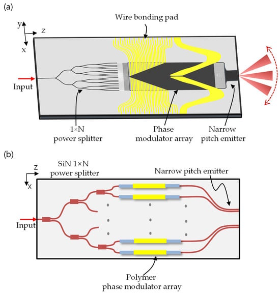
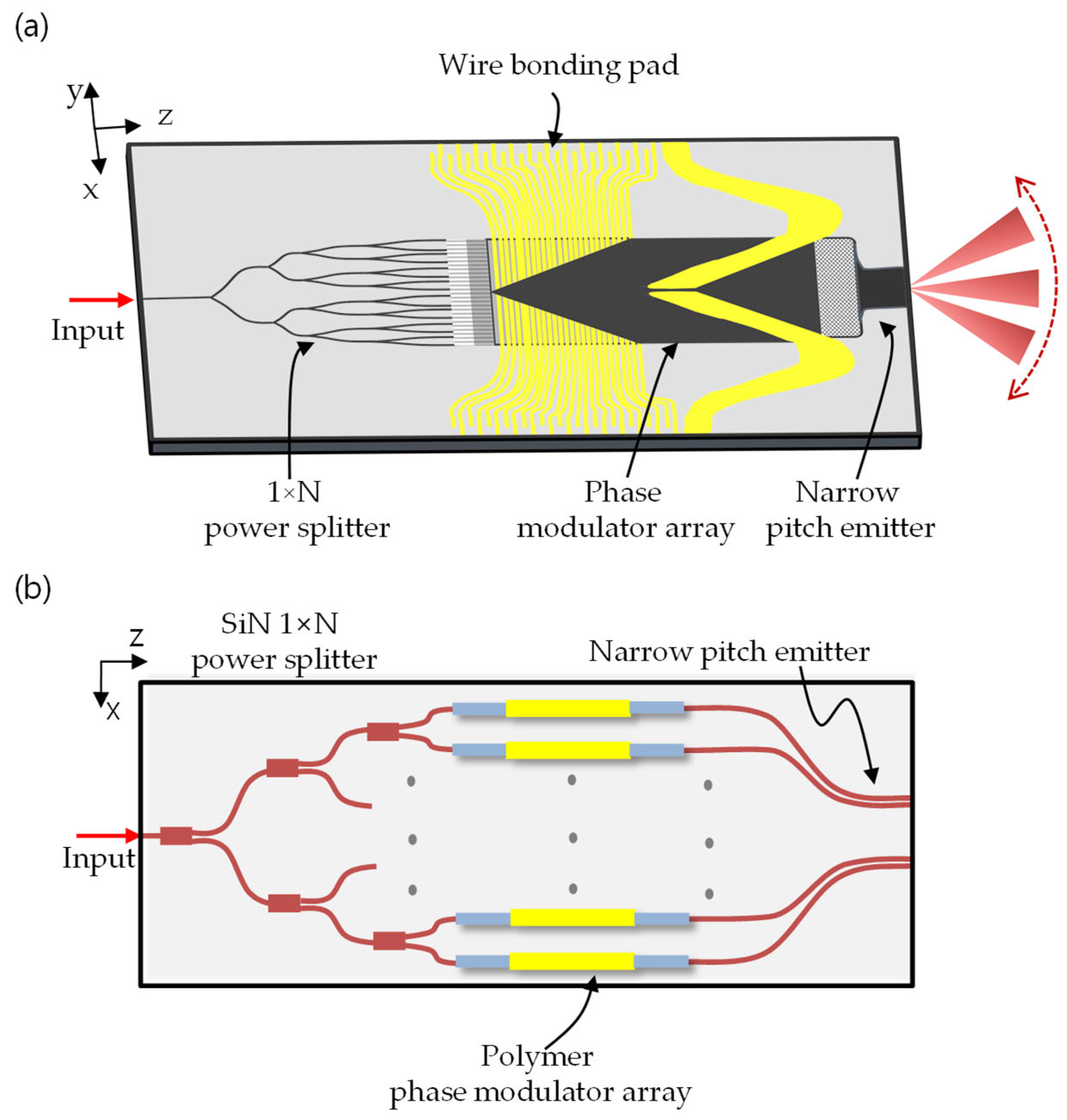
The OPA is designed to be used for a 1550 nm wavelength, which is chosen for its favorable atmospheric transmission characteristics and for the advantage of eye safety. The integrated OPA is made up of a narrow-pitch emitter, an N-channel phase modulator array, and a 1 × N power splitter, all of which are constructed on a single photonic chip, as depicted in Figure 1a. The power splitting and emission sections use silicon nitride (SiN) waveguides because of their compact size relative to polymer waveguides and low propagation loss. Effective TO tuning is made possible by the integration of polymer waveguides with microheaters in the phase modulation (PM) region, as depicted in Figure 1b.
Figure 1.
Configuration of the 128-channel OPA. (a) Complete device schematic of a 1 × N channel OPA, where the incident light is split into N-channels and directed through a polymer waveguide PM array and a narrow-pitch emitter. (b) Top view of the schematic OPA device configuration.
A 7-stage cascade of 1 × 2 multimode interference (MMI) couplers create a 1 × 128 splitter for dividing input optical signal into 128 SiN waveguides. After that, light is directed to the polymer-based phase modulators via SiN-to-polymer transition tapers [23]. After PM, the optical signal passes through another taper and is guided to a closely spaced array of output waveguides. Constructive interference of the in-phase emissions forms a forward-propagating beam. To minimize coupling loss at the fiber-to-chip interface, a tapered spot-size converter with a width of 0.2 µm is implemented at the input facet. This taper achieves an estimated coupling loss of approximately 0.9 dB per facet when interfaced with ultra-high numerical aperture (UHNA) fibers. Additional details regarding the device design and fabrication process can be found in our previous publication [23].
3. Optical Packaging
3.1. Polishing of Waveguide End-Facet
The optical packaging strategy utilizes a fiber V-groove for input edge-coupling with the output facet radiating the beam directly into free space. To ensure efficient optical coupling at the light injection and minimize the scattering at emission interfaces, polishing is performed on both the input and output facets of the OPA chip. The UV-curable epoxy (Daikin, Optodyne UV-2100, Osaka, Japan) used in the pigtailing process has a refractive index of 1.4615 at 1550 nm, closely matching that of the optical fiber. Although this index matching helps reduce Fresnel reflections, mechanical dicing often leaves deep striations and chipping with roughness exceeding 1 µm, introducing significant coupling loss. Therefore, the polishing process is necessary to ensure low-loss coupling and eliminate scattering loss.
The process begins with waveguide dicing that ensures the waveguide input and output is exposed to the end of the chip. To eliminate the roughness from waveguide end-facets, we perform polishing using manual polishing machine (R&B, RB 209 MINIPOL, Daejeon, Republic of Korea). First, the diced sample is mounted for planarization of the end-facet during mechanical polishing. Prior to polishing, an abrasive paper is attached on a rotating plate, and the sample is secured in a jig, positioned against the direction of moving plate. Silicon carbide (SiC) abrasive paper is used in sequence, including 600, 1000, and 2000 grit. These steps ensured that the facets are uniform and planarized.
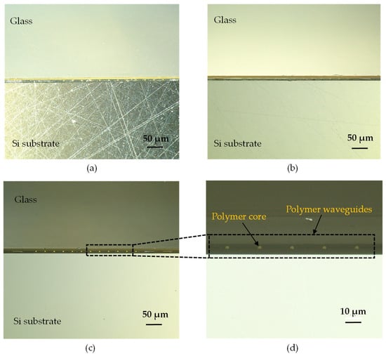
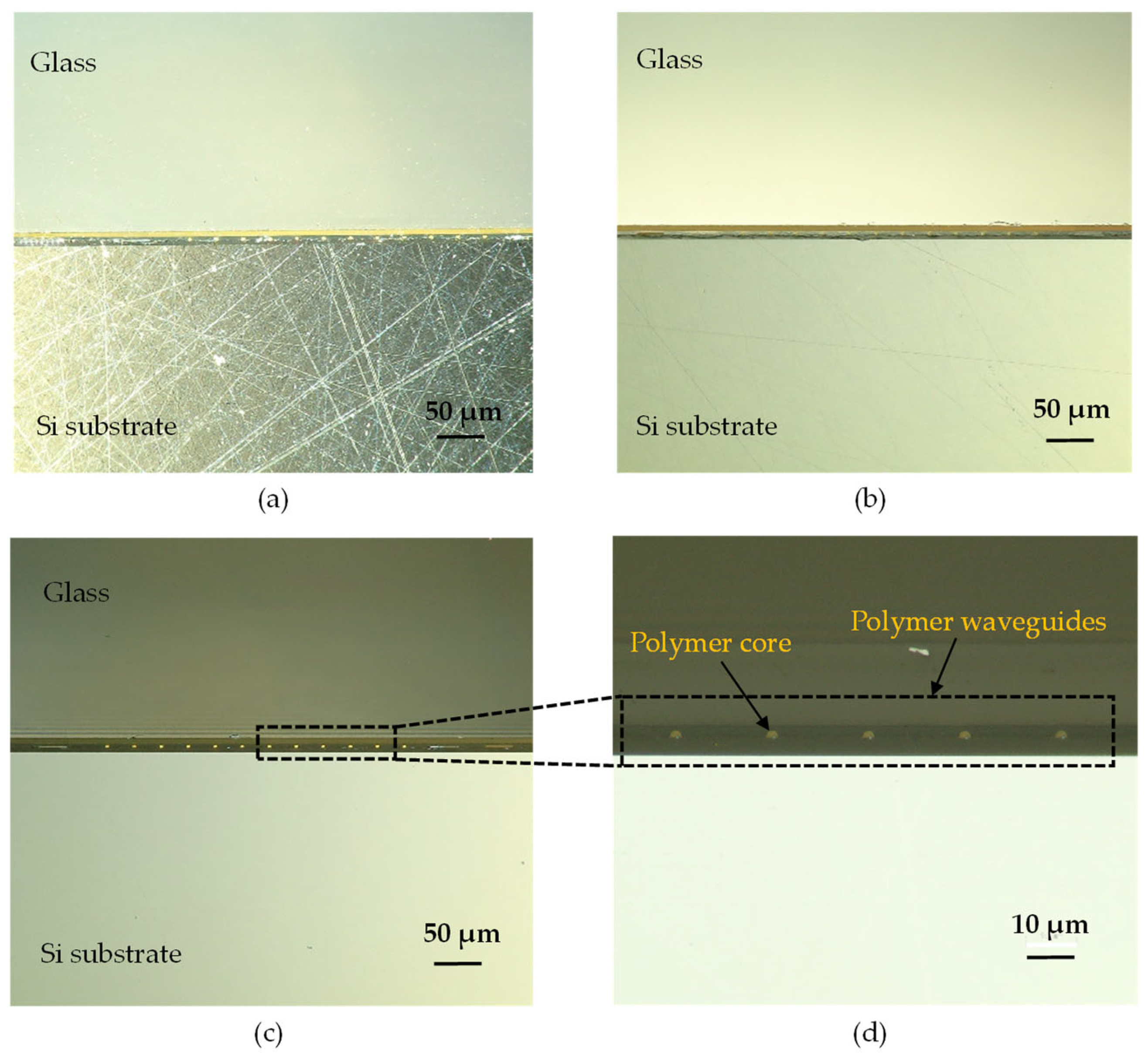
During polishing, the sample is continuously flushed with deionized (DI) water to keep the SiC paper wet, as using dry paper can generate additional scratches. Each grade of SiC paper is applied for 10 min until the deep striations from dicing disappear and only the uniform abrasive marks remain, as depicted in Figure 2a. After preliminary polishing, an ultra-polishing cloth is mounted on the rotating plate for intermediate polishing. A 1 µm polycrystalline diamond suspension is periodically dispensed to keep the cloth wet, and polishing is performed for 10 min. The sample is then cleaned with DI water and dried using a nitrogen (N2) blow gun to remove residual particles, as shown in Figure 2b. For final surface polishing, a DIA-MOL cloth is used together with a 0.06 µm colloidal silica slurry. The slurry consists of amorphous silica nanoparticles dispersed in water, with a silica content of 30%, enabling a smooth, damage-free finish through the polishing. The final polishing step follows the same procedure as the intermediate stage. To remove any remaining slurry, the sample is rinsed with isopropanol (IPA) and DI water, followed by N2 drying.
Figure 2.
Microscopic images of waveguide after each step: (a) preliminary polishing using SiC abrasive papers, (b) intermediate polishing with 1 µm polycrystalline diamond suspension, (c) final surface refinement using 0.06 µm colloidal silica slurry, and (d) magnified view of the polished polymer waveguides.
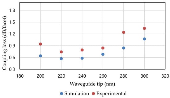
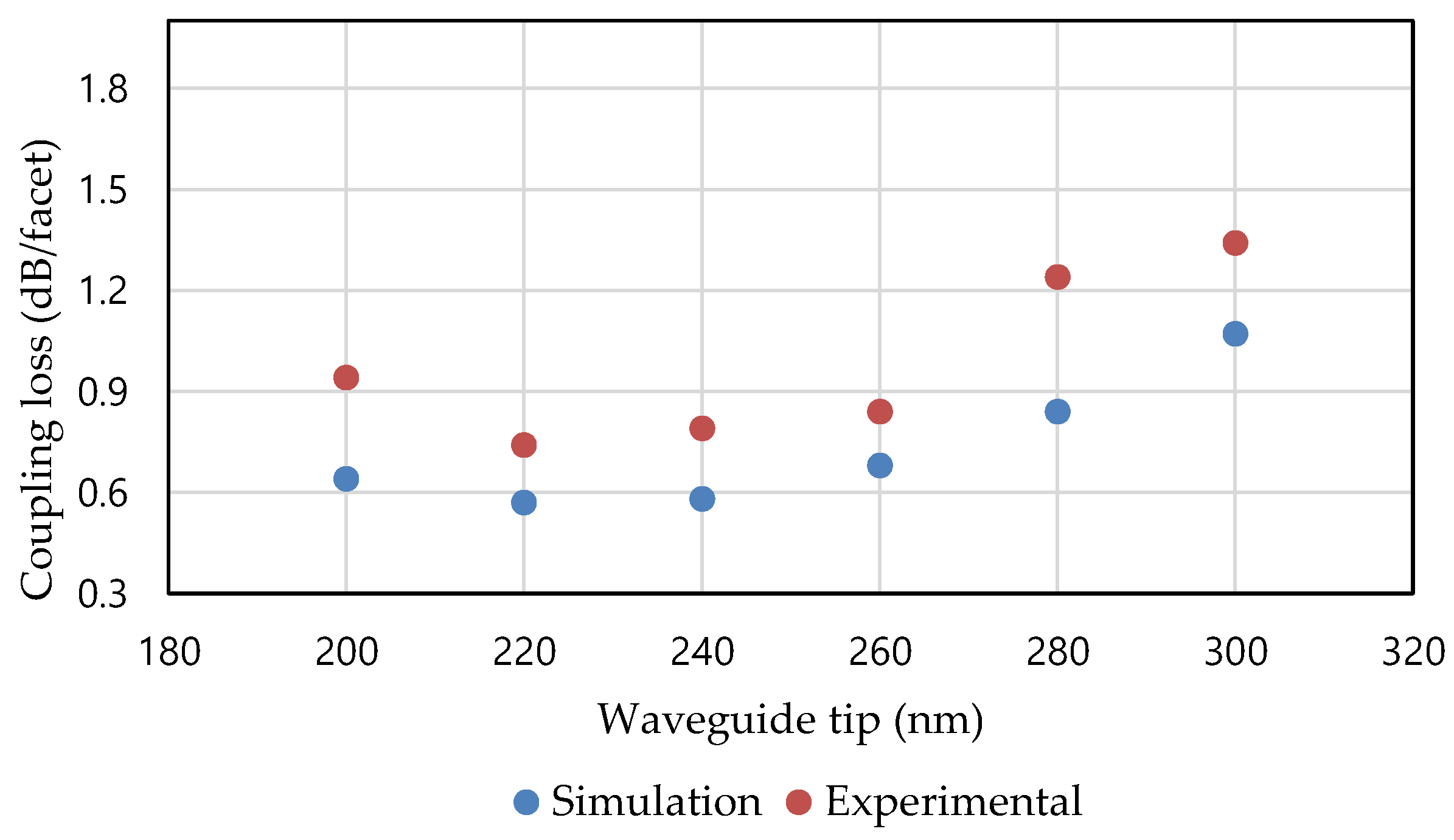
To verify the quality of the facet polishing, polymer waveguides fabricated adjacent to the SiN waveguide region were inspected as depicted in Figure 2c, with a magnified view shown in Figure 2d. Subsequently, insertion loss measurements were conducted across several waveguide tip widths of the SiN spot-size converter (SSC) to determine the coupling loss. The experimental results were then validated against 3D beam propagation method (BPM) simulations, as depicted in Figure 3. Specifically, for a 220 nm waveguide tip width, the simulated coupling loss is 0.57 dB/facet, while the polished samples exhibit coupling losses of 0.74 dB/facet under optimized polishing conditions.
Figure 3.
Coupling losses measured from polished waveguide depending on the waveguide tip width of SiN spot-size converter. The results are compared to the 3D-BPM simulations.
3.2. Fiber-to-Optical Waveguide Alignment
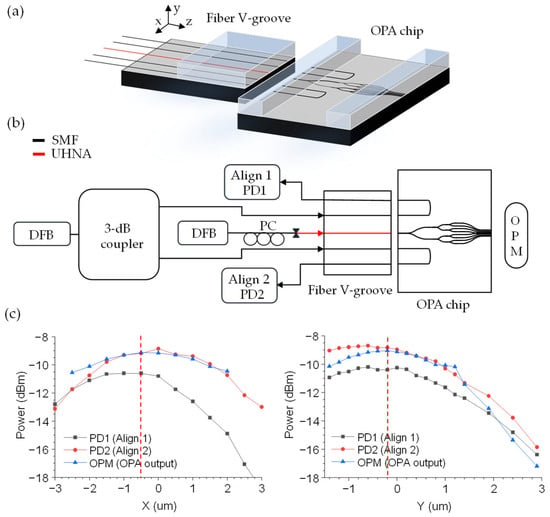
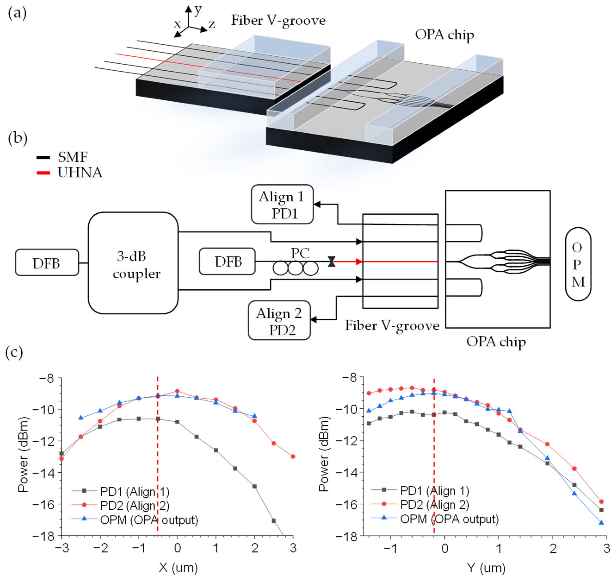
To achieve efficient light injection into the OPA chip, a fiber pigtailing process was implemented using a 5-channel fiber V-groove array and an automated alignment system. Waveguide alignment was typically challenging without real-time output mode monitoring via a charge-coupled device (CCD). However, in this work, we fabricated loop-back waveguide structures adjacent to the OPA input waveguide with the same pitch as the fiber V-groove array, as shown in Figure 4a. By monitoring the returned optical power through the loop-back configuration, precise alignment was achieved. The 5-channel V-groove accommodated both single-mode fibers (SMF) for coarse alignment and ultra-high numerical aperture (UHNA) fibers for precise coupling to the central waveguide as shown in Figure 4b. The alignment system used distributed feedback (DFB) lasers as an optical source and an optical power meter (OPM) for real-time throughput monitoring. A 3 dB coupler and a polarization controller (PC) were included in the setup to split the optical signal and manage the polarization state. The setup enabled continuous monitoring of returned powers during alignment using two photodetectors (PD1 and PD2). In this way, input fiber was precisely aligned to the center input waveguide of the OPA without observing the output mode.
Figure 4.
Fiber alignment setup and characterization. (a) Schematic diagram of the fiber V-groove array aligning to the OPA chip with a loop-back waveguide structure. (b) Experimental setup for detecting the returned power through the loop-back waveguide with two photodetectors (PD1 and PD2), and the power output through the OPA also monitored with an optical power meter (OPM). (c) Power variations during the alignment.
The pigtailing process followed a sequential alignment and bonding workflow. Initial alignment was performed using coarse and fine X-Y stage scanning, enabling sub-micron positioning of the fiber V-groove relative to the waveguide facets, as depicted in Figure 4c. Alignment characterization was conducted by scanning the fiber V-groove across the X and Y directions to determine the peak coupling efficiency.
Once optimal alignment was achieved, UV-curable epoxy was applied to secure the fiber V-groove, while the coupled power was continuously monitored to confirm stability during bonding. To block any radiating light over the top surface of waveguide, an aluminum film was placed nearby the lid glass. The film functions as a spatial filter, ensuring that the optical power meter records only the light guided through the OPA, thereby guaranteeing accurate throughput measurement. The fiber V-groove and OPA were then UV-cured in a controlled N2 atmosphere, which reduced oxygen inhibition and ensured uniform polymerization of the adhesive. This process ensured minimal misalignment throughout handling and curing. After UV curing, the assembly was placed in an oven and kept tension-free to prevent misalignment or contamination and thermally cured at 60 °C for 1 h to provide additional mechanical strength and long-term stability.
Following the packaging procedure, the OPA was enclosed in an aluminum case and prepared for wire bonding onto the printed circuit board (PCB). A thermoelectric cooler (TEC) was mounted on the case using silver epoxy (EPO-TEK, H20E, Billerica, MA, USA) and cured at 120 °C for 15 min, after which a heat sink was attached in the same manner. The PCB was then fixed inside the case with an adhesive and cured at room temperature. A thermistor was added for temperature monitoring, and both the TEC and thermistor were soldered to the PCB. Finally, the pigtailed OPA was mounted on the heat sink using silver epoxy and thermally cured at 80 °C for 3 h.
3.3. Electrical Wire Bonding
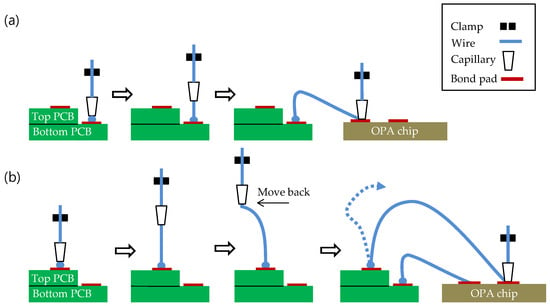
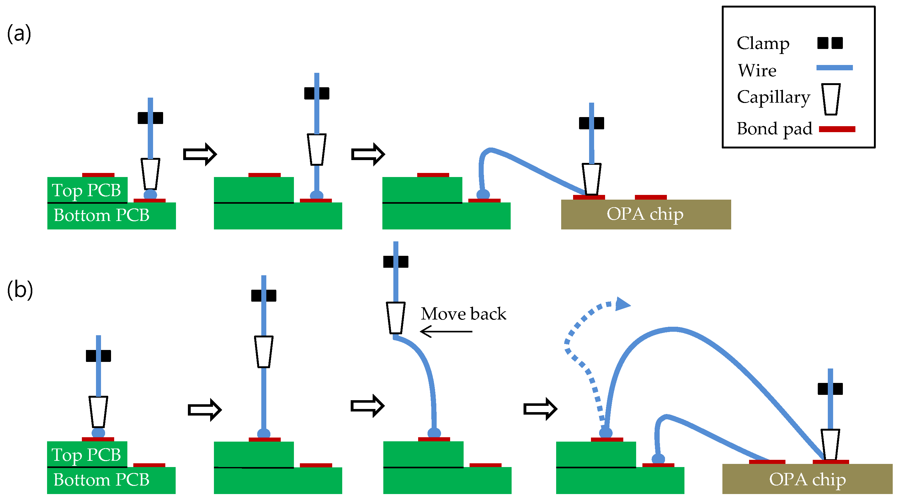
To achieve reliable two-tier wire bonding on the two-layer PCB structure, the loop profiles of bonding wire were carefully optimized to prevent wire shorting, sagging, and breakage. In the first layer, short-loop wire bonding was used to connect the bottom PCB pads to the OPA electrodes, with a loop height minimized to avoid interference and ensure consistent connections across all channels, as shown in Figure 5a. In the second layer, the top PCB was bonded by forming the initial ball bond and then gently pulling back the capillary to create a higher loop, as shown in Figure 5b. This controlled back-drag technique increased loop height, reduced the risk of short circuits between adjacent wires, and provided sufficient clearance above the bottom bonding layer.
Figure 5.
Two-tier wire bonding process between two-layer PCB and OPA chip. (a) First short-loop bonding from the lower PCB forms a low-profile wire. (b) The procedure of wire bonding from the second layer PCB to OPA chip. The dotted blue line shows the initial path of the gold wire, and the solid blue line shows the bonded wire.
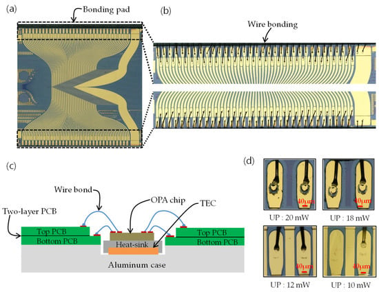
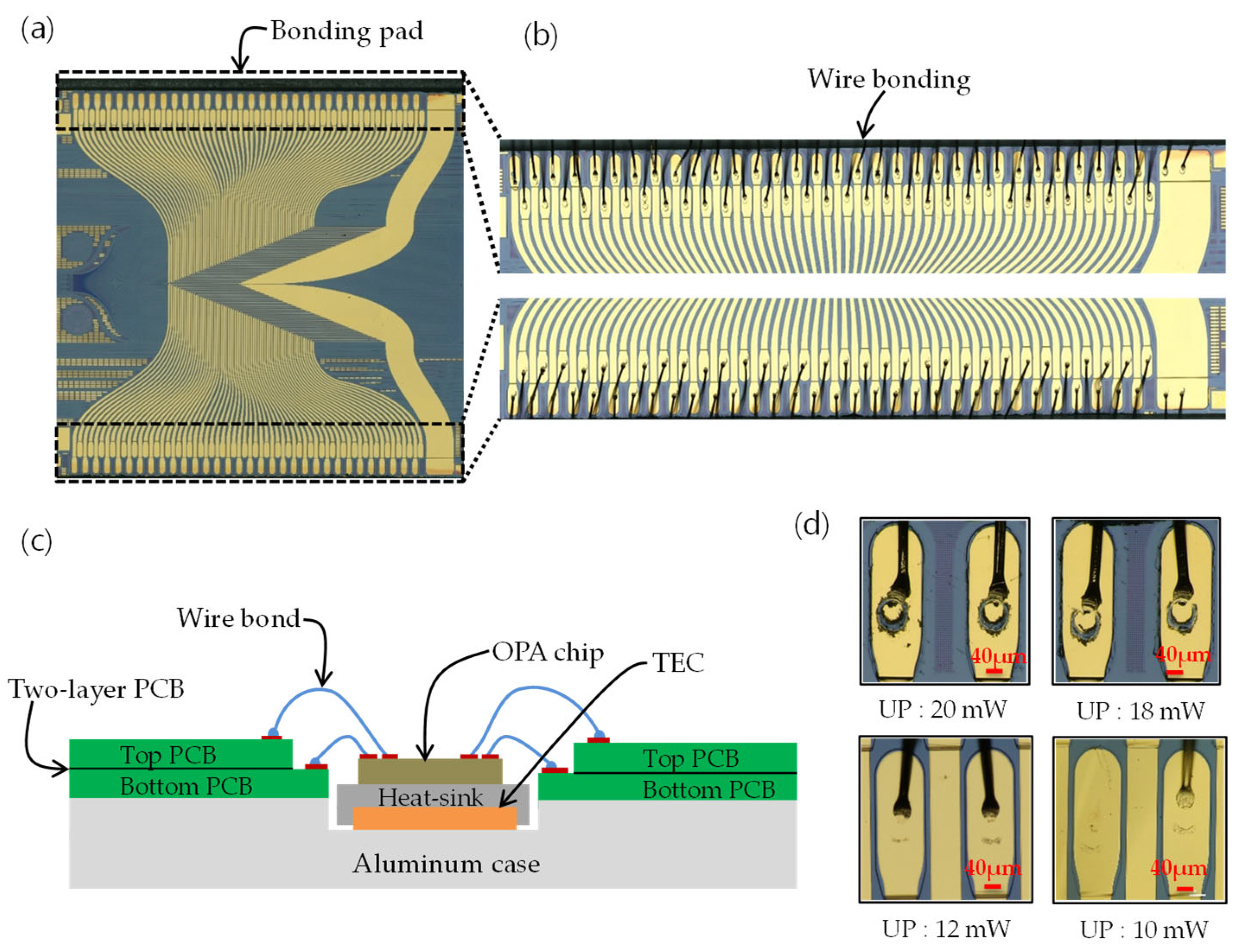
To complete the packaging process, electrical connections for the 128-channel OPA were established using two-tier gold wire bonding. The OPA chip features 120 µm-pitch electrode pads designed to match the minimum pitch of the PCB pads, ensuring precise pad-to-pad alignment and minimizing the chip size, as shown in Figure 6a. Each OPA electrode pad was connected to its corresponding PCB contact pad using a 25 µm diameter gold wire with 70 µm ball size. Wire bonding was performed at room temperature using a manual wire bonder (TPT, HB05, Karlsfeld, Germany) under optimized conditions: ultrasonic power (Pus) of 18 mW, bonding force of 30 mN, and bond time of 130 ms. Microscope images of ball-wedge bonds in Figure 6b, demonstrate uniform bond formation and strong adhesion throughout the array. The cross-sectional schematic configuration of the 128-channel OPA package after wire bonding is shown in Figure 6c.
Figure 6.
Microscopic and schematic illustration of the wire bonding process: (a) 128-channel electrode pad array for two-tier bonding, (b) completed wire bonds ensuring electrical connectivity and mechanical stability, (c) schematic cut-view of the 128-channel OPA package, and (d) bond quality under different ultrasonic power (Pus) conditions of 20, 18, 12, and 10 mW, respectively.
To optimize the bonding parameter, various Pus levels were investigated while maintaining a constant bonding time of 130 ms and bonding force of 30 mN for all tests. For each test condition, 15 bonds were subjected to the pull test to determine the average pull strength. The pull-test results under different Pus conditions are summarized in Table 1. At high Pus values (20–22 mW), the bonds showed moderate pull strength, but it had high risk of damaging the electrode pads. Such excessive bonding strength could reduce the long-term reliability of the device by inducing structural stress on the pads. The optimal condition was found at 18 mW, which provided the highest stable pull strength (4.66 gf) without damaging the pads. In contrast, low Pus levels (10–12 mW) resulted in bond failure, as insufficient ultrasonic energy prevented proper intermetallic formation. These trends are consistent with the microscopic images in Figure 6d, the bonds show insufficient strength, often resulting in bond failure or wire detachment during testing, thereby posing significant risks to device stability.
Table 1.
Pull test results of wire bonds under varying ultrasonic power levels.
4. Packaged Device Inspection
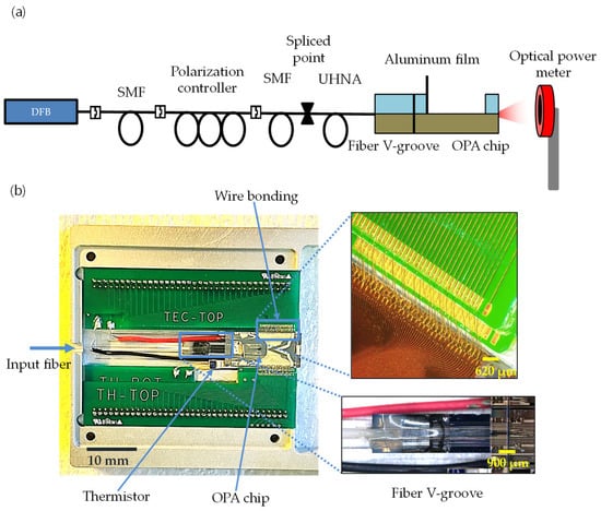
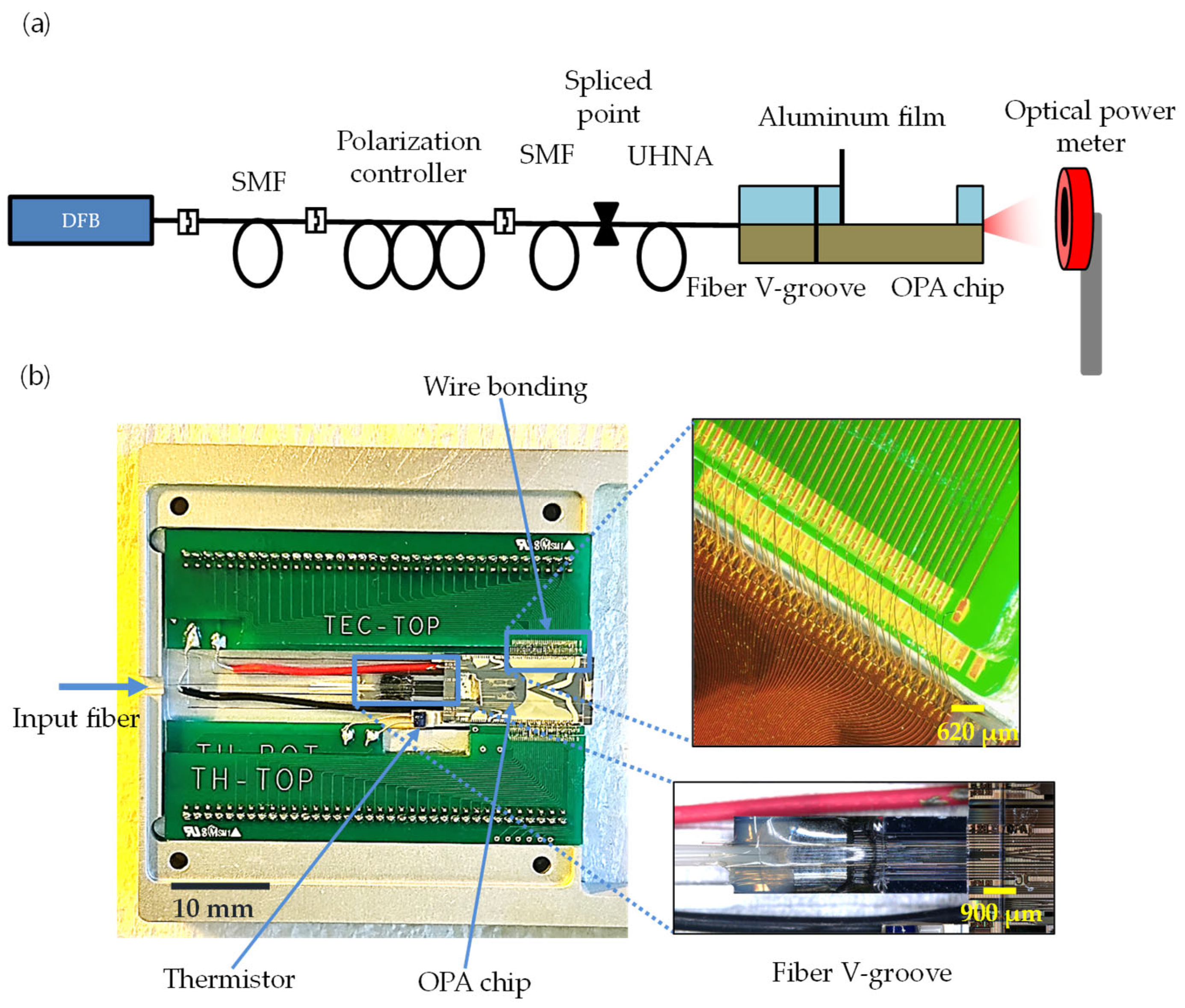
To inspect the packaged OPA, we measured the optical throughput and compared it with the designed value after confirming all the electrical wire bonding. The optical throughput was measured using the setup shown in Figure 7a. A 1550 nm DFB laser was connected to an SMF, followed by a polarization controller to set the transverse electric (TE) input. The output from the controller was then coupled into a UHNA fiber spliced to the SMF. This UHNA fiber in a V-groove was pigtailed to the OPA input facet, forming the complete package shown in Figure 7b. In our measurement setup, the input optical power delivered to the SMF fiber after the polarization controller was set to 0 dBm. The absolute optical power measured at the output of the packaged device was −6.0 dBm.
Figure 7.
Optical throughput measurement and packaged device. (a) Schematic diagram of the optical throughput measurement setup used to evaluate the packaged OPA. (b) Photograph of the fully packaged 128-channel OPA device, where the two-tier wire bonding pad and pigtailed fiber V-groove are magnified in the inset.
To clarify the overall loss budget, we analyzed the components contributing to this loss. For the input fiber, the mode field diameter mismatch between a standard SMF (10.4 µm) and UHNA fiber (4.0 µm) leads to significant loss over 3 dB. To minimize this, we utilized an optimized annealing process on the fusion splicer (Vytran, FFS2000, Morganville, NJ, USA), achieving a splice loss of 0.2 dB. The input coupling loss to the SSC with a tapered tip width of 200 nm was measured at 0.9 dB. The estimated on-chip loss was 4.9 dB, including SiN waveguide propagation loss of 2.4 dB, MMI splitter excess loss of 1.7 dB, SiN-polymer transition loss of 0.2 dB, polymer waveguide propagation loss of 0.2 dB, and the emitter taper excess loss of 0.4 dB. The cumulative sum of these loss components was 6.0 dB, which aligned perfectly with the measured total throughput.
During the packaging process, experiencing elevated baking temperature of 80 °C, the throughput variation remained below 0.2 dB, indicating excellent stability and robustness of the alignment.
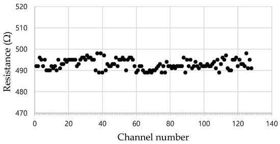
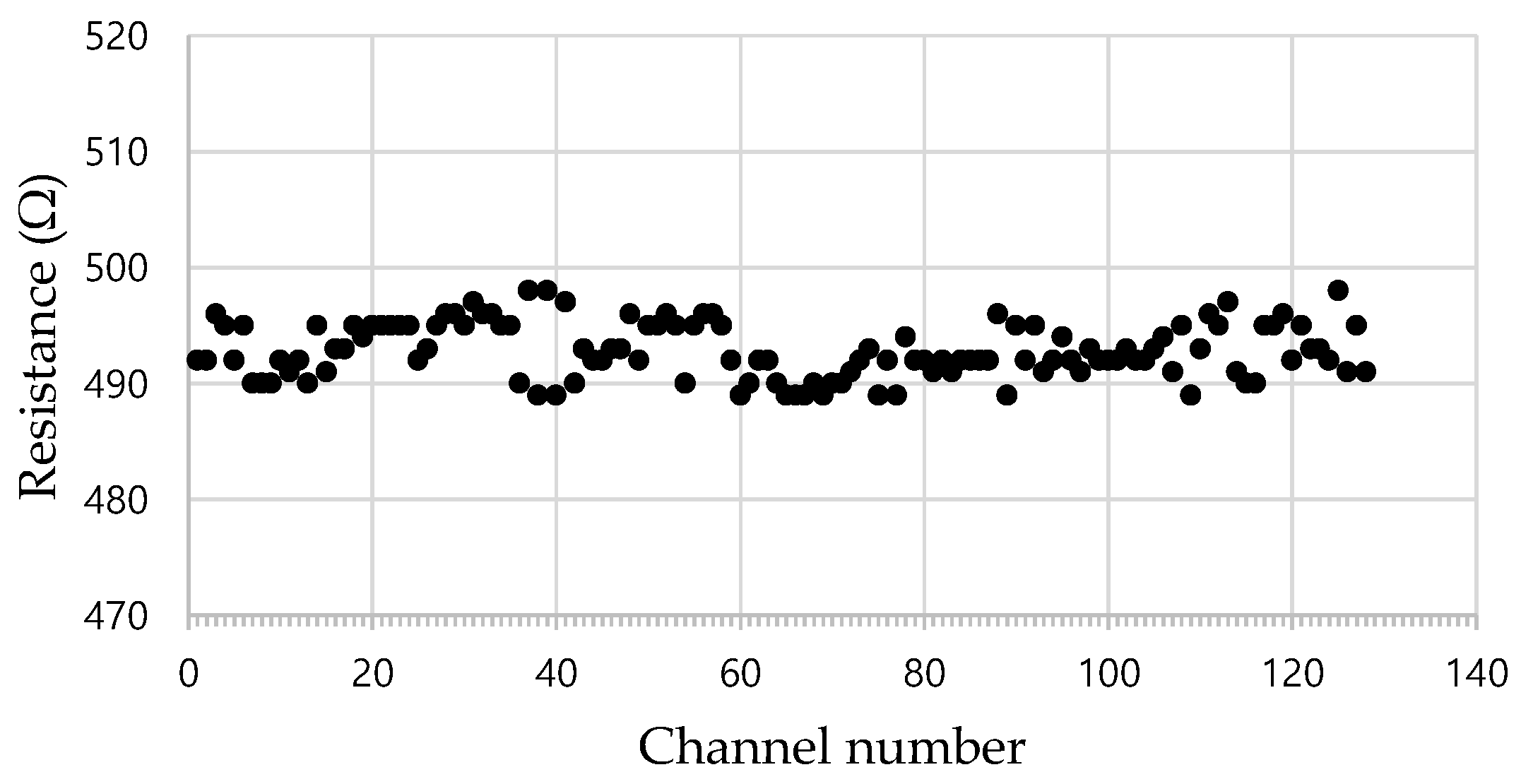
To examine the electrical characteristics of the packaged device, the resistances of all 128 bonded channels were measured after completing the wire-bonding step as shown in Figure 8. All channels maintained proper electrical connections without any open or short circuits, confirming the success of the two-tier wire-bonding process and the reliability of the electrode-to-pad connections. The average resistance was 492.84 Ω with a standard deviation of 2.35 Ω, corresponding to a high uniformity of 0.48% across all channels. In our best experimental result, bonding yield reached 100%, demonstrating that the optimized ultrasonic bonding parameters ensured both strong mechanical adhesion and consistent electrical performance throughout the 128-channel OPA package.
Figure 8.
Electrical resistance measured from 128-channel phase modulators in the OPA device after the wire bonding.
5. Discussion
The low-loss edge coupling employed in this work is significant for high performance LiDARs. Although grating couplers are widely used in silicon photonics due to their relaxed alignment tolerances, they typically suffer from limited bandwidth and high coupling losses [24,25]. In contrast, the edge coupling packaging strategy employed here achieves a low coupling loss of 0.74 dB per facet. Superior coupling efficiency is critical for LiDAR applications, where maximizing the transmitted optical power directly translates to extended detection ranges. Furthermore, the close agreement between the estimated loss budget and the measured total throughput serves as a rigorous validation of the optical packaging quality.
In terms of the electrical interconnects, scaling from 32 to 128 channels necessitated a fundamental shift in the packaging strategy. The implementation of the two-tier bonding technique was instrumental in overcoming the density constraints. As evidenced by the high bonding yield and resistance uniformity, this method effectively manages the spatial crowding of wires. Unlike the rigid silicon substrates, the soft polymer layer absorbs ultrasonic energy, which can lead to either pad damage or weak bonding. By identifying the optimal parameters to navigate this constraint, our work establishes a reliable baseline for scaling to even higher channel counts required for future LiDAR systems.
For practical solid-state LiDAR, the stability of the packaged device is a critical issue. The proposed package maintained stable optical throughput and electrical interconnection throughout the packaging assembly and subsequent device characterization in the laboratory. However, harsh environmental tests were not conducted for this package, which will require further validation for commercialization.
Regarding LiDAR system architecture, it is worth noting that the OPA in this study operates as a transmitter, while the return signal is collected by a separate high-sensitivity detector. Consequently, our packaging focused on emission efficiency and stray light management using an aluminum film to ensure a clear far-field. While our OPA has horizontal steering capability, the vertical beam size was not considered in this work. We acknowledge that vertical collimation is essential for practical LiDAR deployment; therefore, future module-level integration will incorporate cylindrical lenses at the output facet to achieve vertical beam collimation.
6. Conclusions
For the complete packaging of a 128-channel OPA device, the process of end-facet polishing, fiber-to-waveguide coupling, and two-tier wire bonding have been developed. The polishing and fiber pig-tailing process ensured low optical loss and highly stable throughput, achieving a throughput power variation in less than 0.2 dB throughout the entire epoxy baking process. The wire bonding process confirmed a uniform bonding resistance across all 128 channels with a deviation of 0.48%. The developed packaging procedure could pave the way for further advancements in photonic integration for LiDAR, free-space communication, and other related applications.
Author Contributions
Conceptualization, E.-S.L., K.-W.C., J.J., A.S. and M.-C.O.; methodology, A.S. and E.-S.L.; investigation, E.-S.L., K.-W.C., J.J. and M.-C.O.; formal analysis, E.-S.L. and M.-C.O.; data curation, A.S. and E.-S.L.; validation, E.-S.L., K.-W.C. and J.J.; writing—original draft preparation, A.S. and E.-S.L.; writing—review and editing, A.S., E.-S.L. and M.-C.O.; supervision, M.-C.O. All authors have read and agreed to the published version of the manuscript.
Funding
This research was supported by a 2-Year Research Grant by Pusan National University.
Institutional Review Board Statement
Not applicable.
Informed Consent Statement
Not applicable.
Data Availability Statement
The data presented in this study are available on request from the corresponding author.
Conflicts of Interest
The authors declare no conflicts of interest.
Abbreviations
The following abbreviations are used in this manuscript:
| OPA | Optical Phased Array |
| LiDAR | Light Detection and Ranging |
| MEMS | Micro-Electromechanical Systems |
| PIC | Photonic Integrated Circuits |
| FOV | Field Of View |
| CMOS | Complementary Metal-Oxide-Semiconductor |
| SiN | Silicon Nitride |
| PM | Phase Modulation |
| TO | Thermo-Optic |
| MMI | Multimode Interference |
| UHNA | Ultra-High Numerical Aperture |
| SiC | Silicon Carbide |
| DI | Deionized |
| CCD | Charge-Coupled Device |
| SMF | Single-Mode Fibers |
| DFB | Distributed Feedback |
| OPM | Optical Power Meter |
| PC | Polarization Controller |
| PCB | Printed Circuit Board |
| TEC | Thermoelectric Cooler |
| TE | Transverse Electric |
References
- Poulton, C.V.; Yaacobi, A.; Cole, D.B.; Byrd, M.J.; Raval, M.; Vermeulen, D.; Watts, M.R. Coherent solid-state LiDAR with silicon photonic optical phased arrays. Opt. Lett. 2017, 42, 4091–4094. [Google Scholar] [CrossRef] [Scilit] [PubMed]
- Poulton, C.V.; Byrd, M.J.; Russo, P.; Timurdogan, E.; Khandaker, M.; Vermeulen, D.; Watts, M.R. Long-range LiDAR and free-space data communication with high-performance optical phased arrays. IEEE J. Sel. Top. Quantum Electron. 2019, 25, 7700108. [Google Scholar] [CrossRef] [Scilit]
- Rabinovich, W.S.; Goetz, P.G.; Pruessner, M.; Mahon, R.; Ferraro, M.S.; Park, D.; Fleet, E.; DePrenger, M.J. Free Space Optical Communication Link Using a Silicon Photonic Optical Phased Array. In Proceedings of the Free Space Laser Communication and Atmospheric Propagation XXVII, San Francisco, CA, USA, 7–12 February 2015; Volume 9354, p. 93540B. [Google Scholar]
- Yang, S.; Wu, G.; Tang, K.; Yu, F.; Ji, X.; Xin, Y.; Jiang, W. Fast-beam-switching optical phased array for moving objects in wireless optical communication networks. Opt. Lett. 2024, 49, 1961–1964. [Google Scholar] [CrossRef] [Scilit]
- Fukui, T.; Kohno, Y.; Tang, R.; Nakano, Y.; Tanemura, T. Single-pixel imaging using multimode fiber and silicon photonic phased array. J. Light. Technol. 2021, 39, 839–844. [Google Scholar] [CrossRef] [Scilit]
- Wu, L.; Wang, X.; He, X.; Huang, Z.; Huang, X.; Xiong, C. Arbitrary multiple beam forming by two cascaded liquid crystal optical phased arrays. Opt. Express 2018, 26, 17066–17077. [Google Scholar] [CrossRef] [Scilit]
- Wang, Y.; Zhou, G.; Zhang, X.; Kwon, K.; Blanche, P.-A.; Triesault, N.; Yu, K.; Wu, M.C. 2D broadband beamsteering with large-scale MEMS optical phased array. Optica 2019, 6, 557–562. [Google Scholar] [CrossRef] [Scilit]
- Ma, Z.; Wan, Y.; Liang, H.; Fu, Y.; Tang, G.; Zhao, X.; Zhao, S.; Kuang, H.; Zhang, Y.; Wang, J. Photonic integrated optical phased arrays and their applications [Invited]. Chin. Opt. Lett. 2024, 22, 020041. [Google Scholar] [CrossRef] [Scilit]
- Ranno, L.; Gupta, P.; Gradkowski, K.; Bernson, R.; Weninger, D.; Serna, S.; Agarwal, A.M.; Kimerling, L.C.; Hu, J.; O’Brien, P. Integrated photonics packaging: Challenges and opportunities. ACS Photonics 2022, 9, 3467–3485. [Google Scholar] [CrossRef] [Scilit]
- Carroll, L.; Lee, J.S.; Scarcella, C.; Gradkowski, K.; Duperron, M.; Lu, H.; Zhao, Y.; Eason, C.; Morrissey, P.; Rensing, M.; et al. Photonic packaging: Transforming silicon photonic integrated circuits into photonic devices. Appl. Sci. 2016, 6, 426. [Google Scholar] [CrossRef] [Scilit]
- Zimmermann, L.; Preve, G.B.; Tekin, T.; Rosin, T.; Landles, K. Packaging and assembly for integrated photonics—A review of the ePIXpack photonics packaging platform. IEEE J. Sel. Top. Quantum Electron. 2011, 17, 645–651. [Google Scholar] [CrossRef] [Scilit]
- Ibrahim, M.H.; Kassim, N.M.; Mohammad, A.B.; Supa’at, A.S.M. Facet polishing technique for polymer on glass optical waveguide. Optoelectron. Adv. Mater. Rapid Commun. 2009, 3, 223–225. [Google Scholar]
- Schnarrenberger, M.; Zimmermann, L.; Mitze, T.; Bruns, J.; Petermann, K. Facet Preparation of SOI Waveguides by Etching and Cleaving Compared to Dicing and Polishing. In Proceedings of the 1st IEEE International Conference on Group IV Photonics, Hong Kong, China, 29 September–1 October 2004; pp. 72–74. [Google Scholar]
- Son, G.; Han, S.; Park, J.; Kwon, K.; Yu, K. High-efficiency broadband light coupling between optical fibers and photonic integrated circuits. Nanophotonics 2018, 7, 1845–1864. [Google Scholar] [CrossRef] [Scilit]
- Baek, K.; Kim, M.; Kim, H.-S.; Ahn, J.; So, H. Advanced optical integration processes for photonic-integrated circuit packaging. Adv. Mater. Technol. 2025, 10, e01848. [Google Scholar] [CrossRef] [Scilit]
- Mekis, A.; Gloeckner, S.; Masini, G.; Narasimha, A.; Pinguet, T.; Sahni, S.; De Dobbelaere, P. A grating-coupler-enabled CMOS photonics platform. IEEE J. Sel. Top. Quantum Electron. 2010, 17, 597–608. [Google Scholar] [CrossRef] [Scilit]
- Milton, B.; Kwon, O.; Huynh, C.; Qin, I.; Chylak, B. Wire Bonding Looping Solutions for High Density System-in-Package (SiP). In Proceedings of the International Symposium on Microelectronics, Raleigh, NC, USA, 9–12 October 2017; IMAPS: Pittsburgh, PA, USA, 2017; Volume 2017, p. 000426. [Google Scholar]
- Lee, E.-S.; Chun, K.-W.; Jin, J.; Oh, M.-C. Frequency response of thermo-optic phase modulators based on fluorinated polyimide polymer waveguide. Polymers 2022, 14, 2186. [Google Scholar] [CrossRef] [Scilit]
- Shah, A.; Mayer, M.; Zhou, Y.N.; Hong, S.J.; Moon, J.T. Low-stress thermosonic copper ball bonding. IEEE Trans. Electron. Packag. Manuf. 2009, 32, 176–184. [Google Scholar] [CrossRef] [Scilit]
- Kim, T.; Bhargava, P.; Poulton, C.V.; Notaros, J.; Yaacobi, A.; Timurdogan, E.; Baiocco, C.; Watts, M.R.; Stojanović, V. A single-chip optical phased array in a wafer-scale silicon photonics/CMOS 3D-integration platform. IEEE J. Solid State Circuits 2019, 54, 3061–3074. [Google Scholar] [CrossRef] [Scilit]
- Heck, M.J.R. Highly integrated optical phased arrays: Photonic integrated circuits for optical beam shaping and beam steering. Nanophotonics 2017, 6, 93–107. [Google Scholar] [CrossRef] [Scilit]
- Lee, J.S.; Carroll, L.; Scarcella, C.; Pavarelli, N.; Menezo, S.; Bernabé, S.; Temporiti, E.; O’Brien, P. Meeting the electrical, optical, and thermal design challenges of photonic-packaging. IEEE J. Sel. Top. Quantum Electron. 2016, 22, 409–417. [Google Scholar] [CrossRef] [Scilit]
- Lee, E.-S.; Jin, J.; Chun, K.-W.; Lee, S.S.; Oh, M.-C. High-performance optical phased array for LiDARs demonstrated by monolithic integration of polymer and SiN waveguides. Opt. Express 2023, 31, 28112–28121. [Google Scholar] [CrossRef] [Scilit]
- Cheng, L.; Mao, S.; Li, Z.; Han, Y.; Fu, H.Y. Grating Couplers on Silicon Photonics: Design Principles, Emerging Trends and Practical Issues. Micromachines 2020, 11, 666. [Google Scholar] [CrossRef] [Scilit]
- Lomonte, E.; Stappers, M.; Krämer, L.; Pernice, W.H.; Lenzini, F. Scalable and efficient grating couplers on low-index photonic platforms enabled by cryogenic deep silicon etching. Sci. Rep. 2024, 14, 4256. [Google Scholar] [CrossRef] [Scilit]

Disclaimer/Publisher’s Note: The statements, opinions and data contained in all publications are solely those of the individual author(s) and contributor(s) and not of MDPI and/or the editor(s). MDPI and/or the editor(s) disclaim responsibility for any injury to people or property resulting from any ideas, methods, instructions or products referred to in the content. |
© 2026 by the authors. Licensee MDPI, Basel, Switzerland. This article is an open access article distributed under the terms and conditions of the Creative Commons Attribution (CC BY) license.