


Abstract
A novel sense amplifier-based flip-flop (SAFF) is proposed for low-power operation. Since setup time is a key timing metric of a flip-flop, SAFF structures with near-zero setup time are advantageous for high-speed applications. However, reducing D-Q delay by increasing transistor size generally increases internal-node switching and power consumption. To address this trade-off, a conditional capture method using a modified NOR gate is proposed. The modified NOR gate compares D and Q and activates the sense amplifier only when required. As a result, unnecessary internal-node switching is reduced, leading to lower power consumption. In addition, unlike conventional conditional precharge sense amplifier-based flip-flop (CPSAFF), the proposed circuit does not require a separate setup time for precharge, which also helps reduce D-Q delay. The proposed circuit was implemented in the gpdk45nm process. Compared with CPSAFF, the proposed circuit achieved C-Q and D-Q delays of 89% and 66%, respectively, and PDPD-Q values of 82%, 78%, and 75% at switching activities of 0.1, 0.5, and 1.0, respectively. These results indicate that the proposed circuit is suitable for low-power mobile applications with long standby periods.
1. Introduction
The Internet of Things (IoT) has become a part of daily life. Mobile devices and wearable applications are key components of the IoT environment. These devices communicate with surrounding systems, including home appliances. They receive information, transmit commands, and interact with the physical world. Power consumption is a major challenge in mobile and wearable applications [1,2,3]. Device miniaturization is required for portability. However, reduced form factor limits battery capacity [4,5]. In general, operating speed and energy consumption exhibit a trade-off [4,6]. Low-power operation requires low supply voltage and small operating current. These conditions degrade circuit speed. Therefore, circuit design requires a proper balance between power consumption and operating speed [7,8].
Flip-flops are fundamental components of digital systems, especially in application-specific integrated circuits (ASICs). A modern processor may include millions of flip-flops [9]. Their power consumption can account for 20–40% of the total processor power [2,4,5,10,11,12,13]. In a flip-flop, setup time is the interval for which the input must remain stable before the clock edge. Hold time is the interval for which the input must remain stable after the clock edge [14]. The clock-to-output (C-Q) delay is the time required for the output to change after clock arrival. The data-to-output (D-Q) delay is defined as the sum of the setup time and the C-Q delay. Increasing transistor size and operating current can reduce the D-Q delay. However, this approach increases energy consumption. Therefore, reducing the setup time is an effective means of lowering the D-Q delay. A shorter setup time is also advantageous for high-speed operation and for securing timing margin [8,15,16,17]. Accordingly, various techniques have been proposed for setup-time reduction. The sense amplifier-based flip-flop (SAFF) is one of the representative structures [1,2,13,18,19,20,21,22].
A SAFF with near-zero setup time generally consists of a sense amplifier and a latch. At each clock event, the sensing result is delivered to the latch. In this operation, internal-node switching is a major contributor to power consumption [23].
This paper proposes a conditional capture scheme for the SAFF circuit. The scheme is implemented using a modified NOR gate. The sense amplifier operates only when D and Q are different. This operation reduces internal-node switching and lowers power consumption. The rest of this paper is organized as follows. Section 2 reviews the conventional SAFF. Section 3 presents the proposed conditional capture sense amplifier-based flip-flop (CCSAFF) and its operation. Section 4 presents the experimental evaluation. Section 5 discusses the results. Section 6 concludes the paper.
2. Conventional Sense Amplifier-Based Flip-Flop (SAFF)
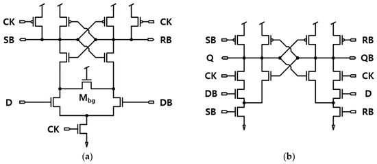
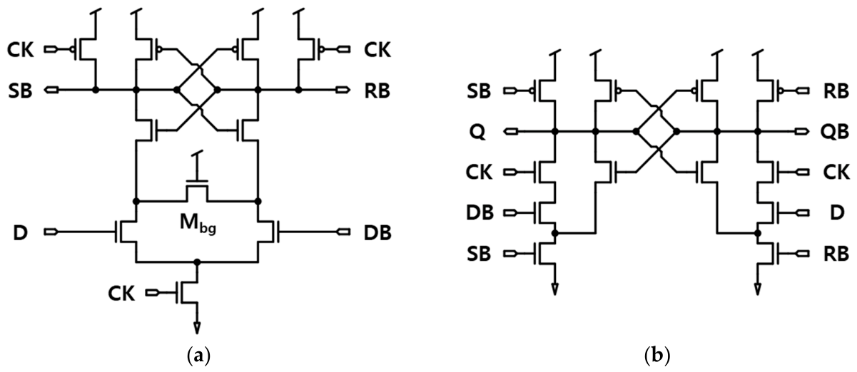
Figure 1 shows the glitch-free SAFF (GFSAFF) circuit. The circuit consists of a sense-amplifier (SA) stage and a latch stage. The SA stage detects the input signal. The latch stage stores and retains the data. The latch stage is composed of a driver circuit and a keeper circuit. The driver circuit receives the output of the SA stage and generates the output Q. The keeper circuit preserves Q [15]. The Q and QB signals are generated in the driver circuit of the latch stage through the SB and RB signals. When CK is low, the SB and RB nodes are precharged to VDD. In a conventional SAFF, when Q is high in the latch stage, a glitch may occur as CK transitions to high. During this event, the Q signal is momentarily discharged. In the proposed circuit, an additional transistor controlled by D and DB is inserted into the driver circuit. This transistor suppresses the glitch-induced energy loss. The Mbg transistor is introduced to improve the stability of SA operation under variations in D and DB during sensing. However, in this SAFF, Mbg remains continuously on. As a result, unnecessary power consumption occurs.
Figure 1.
Glitch-free sense amplifier-based flip-flop (GFSAFF): (a) sense-amplifier stage; (b) latch stage.
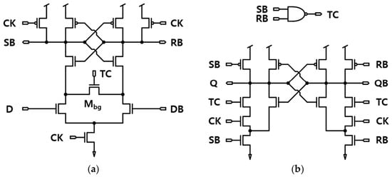
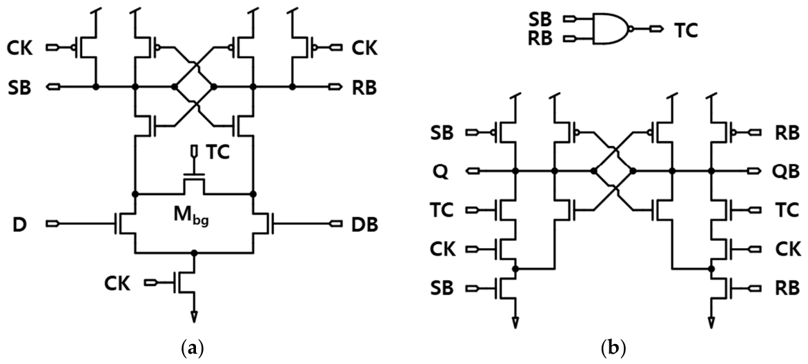
Figure 2 shows transition completion detection SAFF (TCDSAFF) circuit [24]. As in the SA stage, an Mbg transistor is included to ensure operational stability. However, its gate is not fixed at the supply voltage. Instead, it is controlled by the transition-completion signal. The transition-completion signal is generated from the SB and RB signals through an NAND gate. When CK is low, the SB and RB signals are precharged to the supply voltage. Accordingly, the transition-completion signal becomes 0. When CK goes high, either the SB or RB signal is discharged to 0 according to the input D. At the same time, the transition-completion signal changes to 1, indicating completion of SA operation. Because the Mbg transistor is not always active, power consumption can be reduced. However, this advantage may be offset by the continuous operation of the NAND gate.
Figure 2.
Transition completion detection sense amplifier-based flip-flop (TCDSAFF): (a) sense-amplifier stage; (b) latch stage and transition completion detection gate.
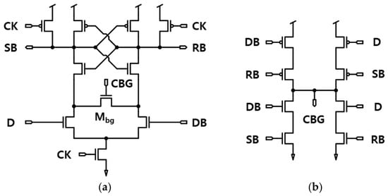
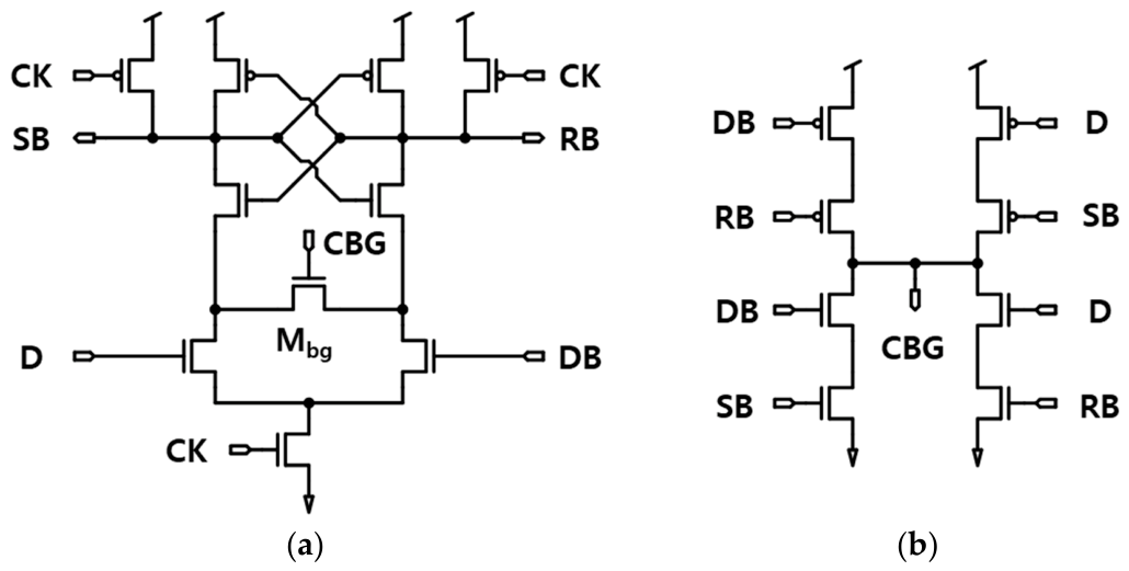
Figure 3 shows the conditional bridging SAFF (CBGSAFF) proposed [2]. In the SA stage, the Mbg transistor is controlled by the CBG signal. As shown in Figure 3b, CBG denotes the conditional bridge signal. When both SB and RB are at the supply voltage, CBG remains at 0. Even if either SB or RB is discharged, CBG remains at 0. However, when D or DB changes under this condition, CBG transitions to 1. Therefore, the CBG signal activates the Mbg transistor only when D or DB changes and the operation of the Mbg transistor is required. However, because the precharge of the SB and RB nodes is performed together with the SA-stage operation, switching activity still increases in proportion to power consumption.
Figure 3.
Conditional bridging sense amplifier-based flip-flop (CBGSAFF): (a) sense-amplifier stage; (b) conditional bridge.
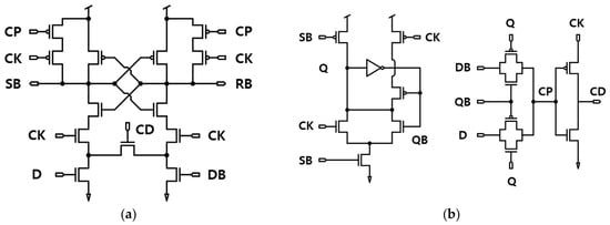
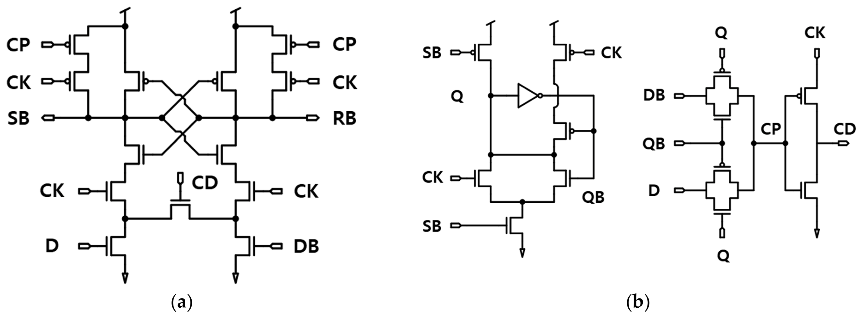
Figure 4 shows the conditional precharge SAFF (CPSAFF) circuit proposed [25]. The precharge method in the sense-amplifier stage differs significantly from those reported in previous studies. The operation is controlled by the CP signal. The CP signal compares the stored value Q with the current input D. It is set to 1 when the two values are identical and to 0 when they are different. Accordingly, the SA stage performs the precharge operation only when D and Q are different. This approach avoids unnecessary precharge operations and thus reduces power consumption. However, it requires an initial setup interval for the comparison of D and Q. In addition, the precharge operation introduces extra delays.
Figure 4.
Conditional precharge sense amplifier-based flip-flop (CPSAFF): (a) sense-amplifier stage; (b) latch stage.
3. Conditional Capture Sense Amplifier-Based Flip-Flop (CCSAFF)
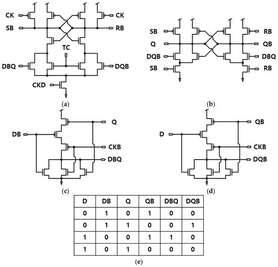
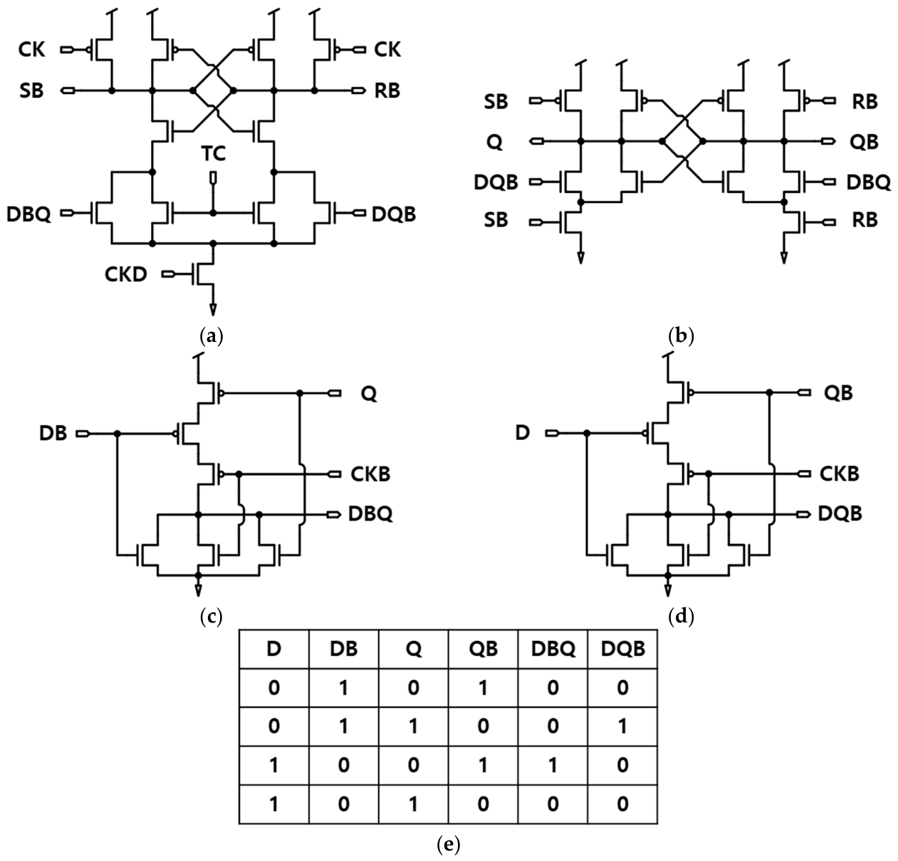
Figure 5 illustrates the proposed circuit. In the proposed SA stage, the D and DB signals are not directly applied. Instead, sensing is performed using the DBQ and DQB signals generated by the conditional capture gate. As shown in Figure 5d, the conditional capture gate has a modified NOR gate structure. In this structure, CKB operates as a switch. When CKB is high, the output remains 0. When CKB is low, the output follows the NOR logic. As in the conventional TCDSAFF, the TC signal is generated by an NAND gate driven by SB and RB. The latch stage consists of a driver circuit and a keeper circuit. The driver circuit controls the transitions of Q and QB through SB, RB, DQB, and DBQ. The keeper circuit preserves Q and QB by means of a cross-coupled latch structure during the low phase of CK. Similar to DQB, DBQ and CKD are generated by the proposed NOR gate. DBQ is generated by DB and Q. CKD is generated by grounding the two inputs other than CKB. As shown in Figure 5e, the SA stage is activated only when Q and D are different. When Q is 0 and D is 1, DBQ is 1 and DQB is 0. When Q is 1 and D is 0, the opposite condition occurs. When Q and D are equal and CK is low, DBQ and DQB are both 0. Under this condition, the SA stage is disabled. Figure 5b shows that the driver circuit in the latch stage is structurally simplified. Because the DQB and DBQ signals are controlled by CK, glitch generation is suppressed. The reduced driver depth is beneficial for low-voltage operation and delay reduction. Therefore, the simplified structure provides an advantage in high-speed operation. During sensing, the input D may fluctuate. To maintain operational stability, the proposed circuit employs a TC-controlled transistor to establish a pull-down path, similar to the conventional structure. Unlike the conventional approach, a change in D forces both DBQ and DQB to 0. Under this condition, the pull-down path is activated by the TC signal. The SA-stage enable signal, CKD, is a delayed version of CK generated by the modified NOR gate, as in DBQ and DQB. This delay is introduced to compensate for the NOR-gate propagation delay and to minimize its impact on sensing operation.
Figure 5.
Proposed conditional capture sense amplifier-based flip-flop (CCSAFF): (a) sense-amplifier stage; (b) latch stage; (c) conditional capture gate for signal DBQ; (d) conditional capture gate for signal DQB; (e) truth table of DBQ, DQB when CK = ‘high’.
A conditional capture method has been proposed in which the SA is activated only when D and Q differ. However, in the previous conditional scheme, precharge for the next sensing operation is not performed during the low phase of CK alone. Instead, precharge begins only after D is applied and a mismatch between D and Q is detected while CK is low. Therefore, an additional comparison interval is required. This interval functions as the setup time and increases the D-Q delay. In addition, Q is driven only by SB. Thus, when Q changes in response to D, its switching speed is lower than that of the conventional cross-coupled latch structure using complementary SB and RB signals. In the proposed method, the SA performs the precharge while CK is low. Therefore, as in the conventional SAFFs without conditional operation, the setup time is nearly zero. When D and Q have the same value, the pull-down path of the proposed SA is disabled by the output of the modified NOR gate. As a result, SB and RB retain their precharged values. Accordingly, no additional power is consumed during the next low phase of CK for the precharge. In addition, the cases in which DQB and DBQ become high correspond to the discharge conditions of Q and QB, respectively. Therefore, the latch stage does not require an additional transistor for glitch prevention. Compared with the conventional latch stage, the proposed latch stage is simplified. This simplification reduces the burden of transistor upsizing for minimizing the D-Q delay. However, the modified NOR gate used for D–Q comparison increases area overhead. In addition, if D and DB change before SB and RB respond during sensing operation, the pull-down path of the SA may be removed. Therefore, a strict hold-time constraint is required.
The operation of the proposed circuit is examined with respect to the input D and the stored data Q. DB and QB are the complementary signals of D and Q, respectively.
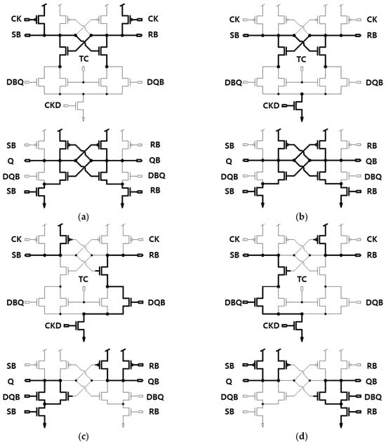
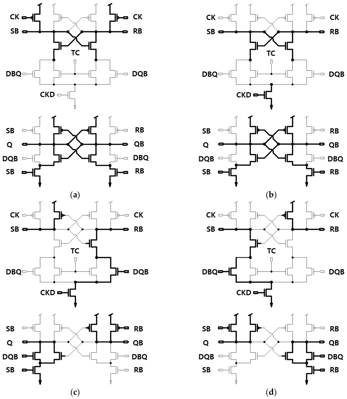
Case (1): CK = 0.
When CK is low, SB and RB are precharged to VDD. The delayed clock signal, CKD, also remains low. Therefore, the SA stage is inactive. Because CKD is low, DBQ and DQB remain low. Since SB and RB are both at VDD, TC remains low regardless of the values of D and DB. In the latch stage, the cross-coupled latch holds the stored values of Q and QB. The corresponding operation is illustrated in Figure 6a.
Figure 6.
Operation of conditional capture sense amplifier-based flip-flip (CCSAFF): (a) CK = 0; (b) CK = 1, D = Q; (c) CK = 1, D = 0, Q = 1; (d) CK = 1, D = 1, Q = 0.
Case (2): CK = 1, D = Q
When CK transitions to high, both DBQ and DQB remain at 0 because D and Q have the same value. As a result, SB and RB do not change, and TC also remains unchanged. Since DBQ and DQB are both 0 in the latch stage, the driver circuit is not activated. Therefore, the latch stage maintains the current values of Q and QB. The resulting operation is illustrated in Figure 6b.
Case (3): CK = 1, D = 0, Q = 1
When CK transitions to high, DQB goes high and DBQ remains low. Under this condition, RB is discharged, whereas SB remains at VDD. After RB is sufficiently discharged, TC transitions to high, allowing SA operation to continue even if D changes to 1. When RB reaches 0, the driver circuit in the latch stage drives QB to VDD. At the same time, Q is discharged to 0 through SB and DQB. The corresponding operation is shown in Figure 6c.
Case (4): CK = 1, D = 1, Q = 0
When CK transitions to high, DQB becomes 0 and DBQ becomes 1. The subsequent operations of the SA stage and the latch stage proceed in the same manner as in the previous case. The resulting operation is shown in Figure 6d.
4. Simulation Results
To verify the operation of the proposed conditional capture sense amplifier-based flip-flop (CCSAFF) and evaluate its performance, simulations were conducted using Cadence. The gpdk45nm process was adopted. The threshold voltages of the NMOS and PMOS transistors were 0.38 V and 0.36 V, respectively. The simulations were performed at a supply voltage of 1.0 V and a clock frequency of 1 GHz. Power consumption, setup time, hold time, and C-Q and D-Q delays were evaluated as functions of switching activity. To evaluate power efficiency, the power-delay product was examined under varying switching activities. To assess operational stability against supply-voltage variation, 200 Monte Carlo simulations were conducted. For performance comparison, the proposed circuit was compared with GFSAFF, TCDSAFF, CBGSAFF, and CPSAFF.
4.1. Conditional Capture Operation
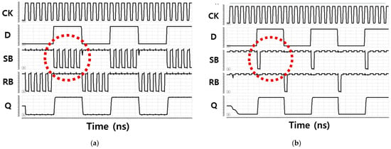
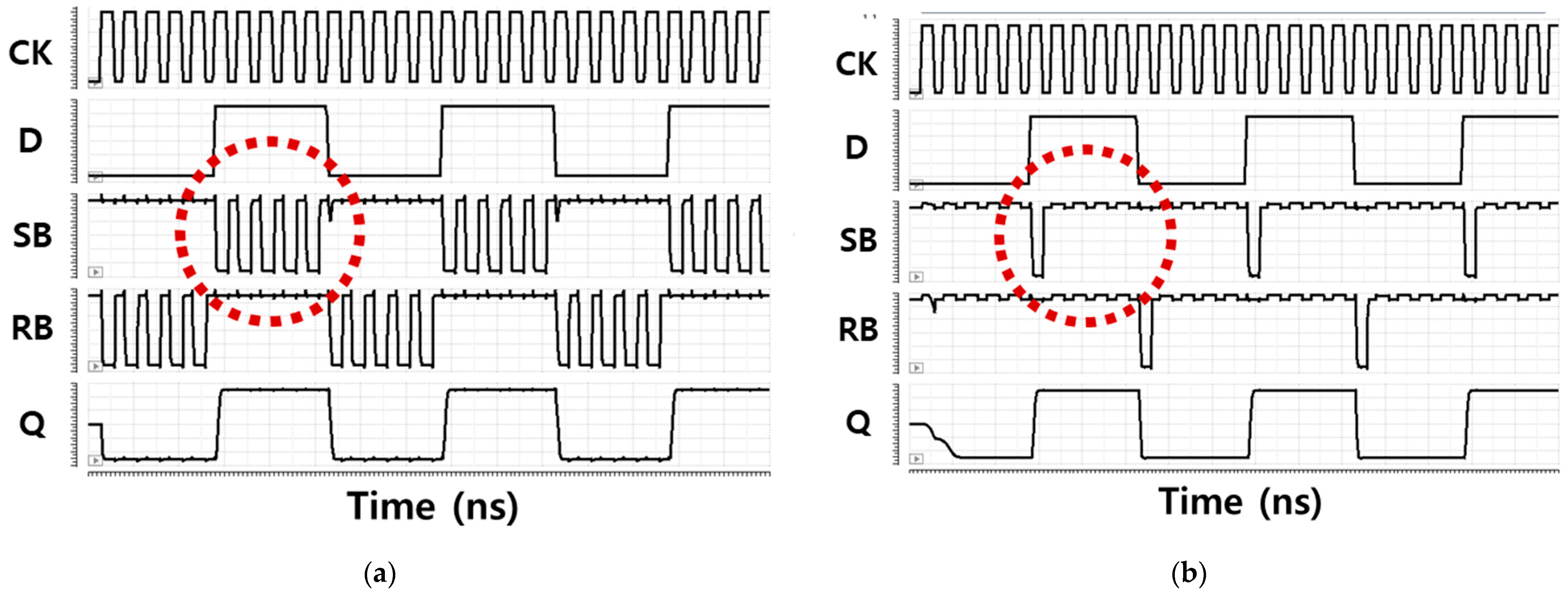
Figure 7 compares the operations of the GFSAFF and the proposed CCSAFF. As can be seen through SB within the red circle in Figure 7a, the GFSAFF exhibits repeated voltage transitions at either SB or RB whenever CK is applied, independent of data activity. Accordingly, the sense-amplifier stage is activated at every clock event. The SB or RB node is then precharged immediately after the sensing operation. By contrast, as can be seen through SB within the red circle in Figure 7b, in the proposed CCSAFF, the SB and RB nodes maintain their precharged levels when the stored value Q matches the input D. In this condition, only small voltage fluctuations are observed at SB and RB. These fluctuations occur because the nodes become floating during the high phase of CK and are affected by clock coupling. Since the internal SB and RB nodes do not undergo precharge or discharge when D and Q are equal, the proposed CCSAFF achieves lower power consumption.
Figure 7.
Changes in prechagre operation of sense amplifier-based flip-flop (SAFF): (a) GFSAFF; (b) proposed CCSAFF.
4.2. Power Consumtion with Switching Activity
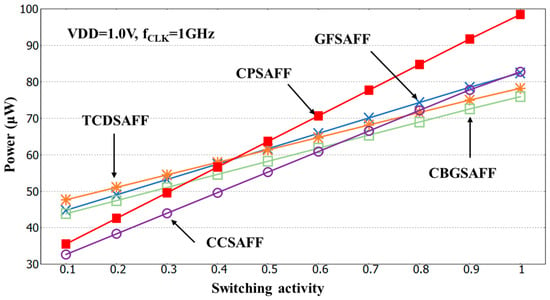
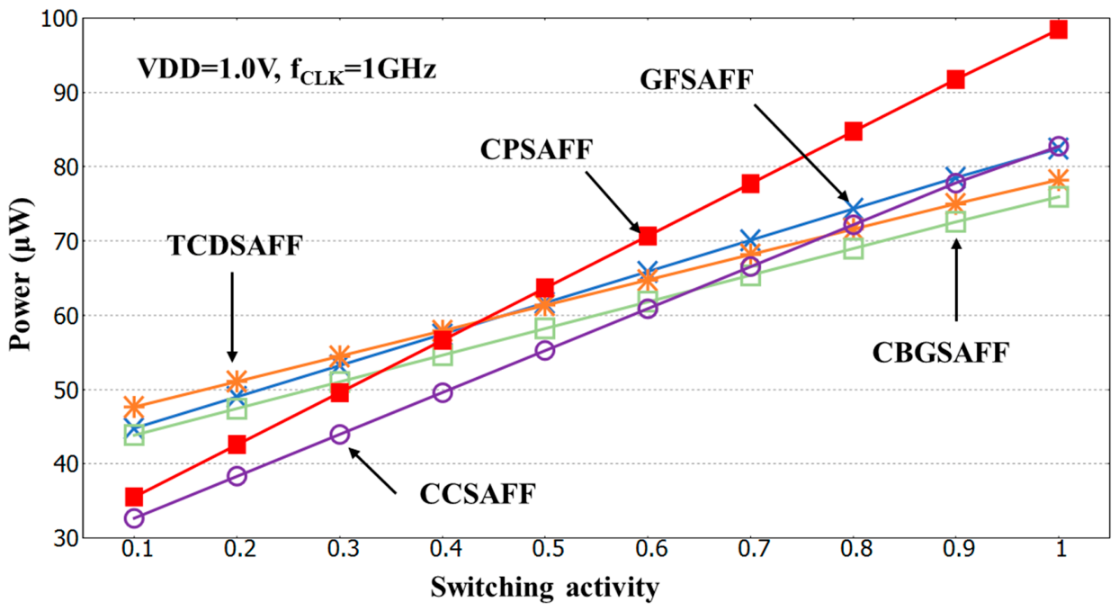
Figure 8 shows the power consumption measured according to switching activity. Data switching is defined as a change in the input D with respect to its previous value at the clock edge. A switching activity of 1.0 means that D changes at every clock cycle. The measurements were performed at 1.0 V and 1 GHz. Power consumption increases as switching activity increases.
Figure 8.
Power consumption comparison with switching activity.
This is because power is consumed during the precharge and discharge operations of the sense-amplifier stage and during the switching of Q and QB in the driver circuit of the latch stage. In general, switching activity in digital circuits is often assumed to be around 10% for representative workloads, although the exact value depends on the application and input patterns [25]. At a switching activity of 0.1, the proposed CCSAFF consumes 32.7 μW. This is 68.6% and 92% of the power consumed by GFSAFF and CPSAFF, respectively. In the CCSAFF, the sense-amplifier stage does not operate when switching activity is absent. As a result, the proposed circuit exhibits low power consumption under low-switching conditions. When the switching activity is 0.6 or lower, it shows the lowest power consumption among the compared circuits. The proposed CCSAFF uses a modified NOR gate at the input of the sense-amplifier stage to compare the stored value Q with the current input D. This comparison determines whether the sense amplifier is activated. To avoid setup time caused by the propagation delay of the modified NOR gate, the clock input to the sense-amplifier stage is also applied through the same gate. However, this additional circuitry increases power consumption as switching activity increases. At a switching activity of 1.0, the power consumption reaches 82.7 μW. This value is higher than the minimum value of 76 μW obtained for the CBGSAFF. This is because the modified NOR gate used for D-Q comparison contributes to increased power consumption at high switching activity.
Low-power operation is a key requirement for mobile applications. Under a static condition in which neither the clock nor input D changes, the power consumptions of GFSAFF, TCDSAFF, CBGSAFF, and CPSAFF were 1.09 nW, 1.05 nW, 1.10 nW, and 1.12 nW, respectively. The proposed CCSAFF consumed 1.11 nW. Although it did not provide the best static-power performance, the difference was marginal. In contrast, at a switching activity of 0.01, the power consumptions of GFSAFF, TCDSAFF, CBGSAFF, CPSAFF, and CCSAFF were 41.0 μW, 44.6 μW, 40.6 μW, 29.4 μW, and 27.4 μW, respectively. These results indicate that clock-induced switching at internal nodes significantly affects power consumption. Since the proposed CCSAFF achieves the lowest power consumption under low-switching conditions, it is well suited for applications with long standby times.
4.3. Set-Up, Hold Time C-Q, and D-Q Delay
Setup time and hold time are fundamental timing parameters of a flip-flop. They are defined as the minimum times for which the input data must remain stable before and after the active clock edge, respectively. The valid time window corresponds to the interval over which the input data is required to remain stable for correct operation, and it is given by the sum of setup time and hold time. The C-Q delay is defined as the propagation delay from the active clock edge to the output transition. The D-Q delay is defined as the total delay from the arrival of input data to the resulting output transition, and it is conventionally expressed as the sum of setup time and C-Q delay [6]. Therefore, when the setup time is defined as zero, the D-Q delay reduces to the C-Q delay. To determine the setup and hold times, the pulse width of input D was swept relative to CK, and the resulting timing variation at output Q was analyzed. The setup and hold times were defined as the points at which the delay of output Q exhibited a deviation of 5% or more [14].
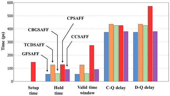
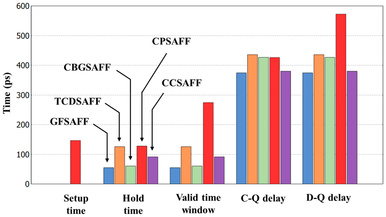
Figure 9 compares the timing performance of the proposed CCSAFF with that of conventional circuits. All simulations were performed at a supply voltage of 1.0 V. In general, SAFF structures have the advantage of near-zero setup time. However, CPSAFF requires a setup interval for the comparison between D and Q and for the precharge operation. As a result, CPSAFF exhibited a setup time and valid time window of 274 ps. The proposed CCSAFF achieved 91.4 ps.
Figure 9.
Comparison of the timing performance with sense amplifier-based flip-flops.
C-Q delay is the time from the clock edge to the output transition. It is determined by the sensing speed of the SA stage and the driving strength of the latch stage. The proposed CCSAFF has fewer transistor stacks in the latch-stage driver. This structure is favorable for driving Q and QB. The C-Q delay of CCSAFF is 379.8 ps. This value is comparable to that of GFSAFF with the C-Q delay of 374.3 ps. In the proposed CCSAFF, D is not directly applied to the sense-amplifier stage. Instead, a modified NOR gate compares D and Q, and the sense amplifier operates based on the comparison result. The hold time of CCSAFF is 91.4 ps, whereas that of CPSAFF is 127.6 ps. The D-Q delay of CCSAFF is 379.8 ps. In contrast, the D-Q delay of CPSAFF is 572.6 ps due to its setup-time requirement. These results indicate that the proposed CCSAFF provides improved timing performance compared with CPSAFF. The near-zero setup time of the proposed CCSAFF improves the timing margin. In addition, its short C-Q and D-Q delays demonstrate its suitability for high-speed operation.
4.4. Power Delay Product
The power-delay product (PDP) is defined as the product of power consumption and delay. It is a metric used to evaluate the trade-off between speed and energy efficiency.
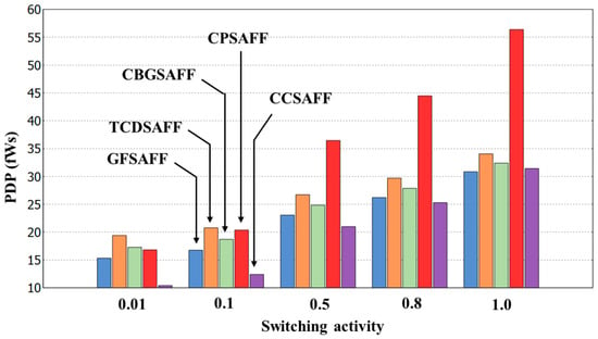
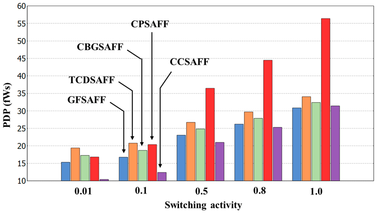
Figure 10 compares D-Q delay and power consumption according to switching activity at a supply voltage of 1.0 V. The proposed CCSAFF shows the smallest PDP in all cases. This result is attributed to the conditional capture scheme. It suppresses the switching of internal nodes associated with clock operation. As a result, power consumption is reduced. Although CPSAFF uses a conditional precharge scheme, its PDP remains relatively high. This is mainly due to the increase in D-Q delay caused by the setup time.
Figure 10.
Power X D-Q delay with switching activity.
In particular, at a switching activity of 0.01, which corresponds to an idle condition, the proposed CCSAFF shows a PDP of about 10.4 fWs. This value is about 62% of the 16.8 fWs of CPSAFF. These results indicate that CCSAFF is more suitable for mobile applications with long standby periods.
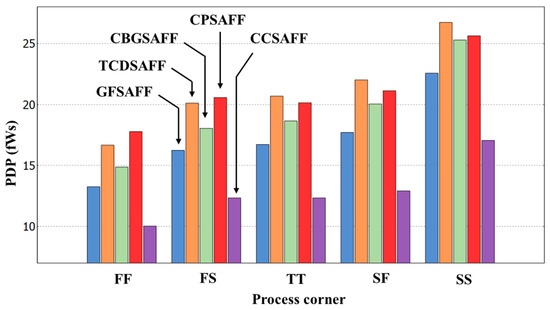
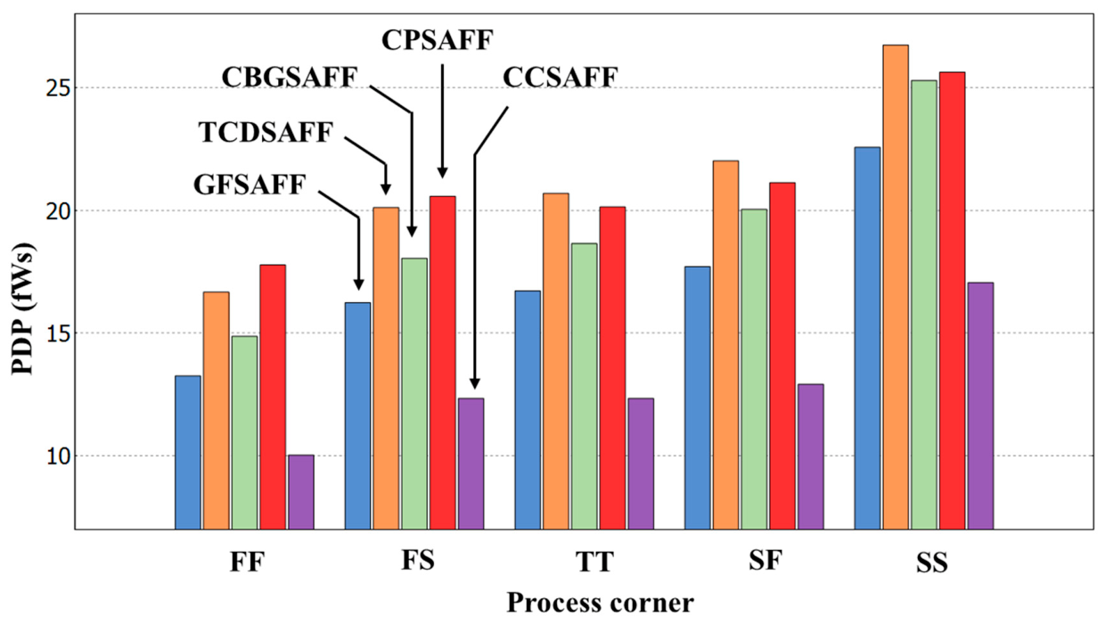
Figure 11 shows the PDP as a function of process corner at a switching activity of 0.1. In the FF corner, the larger driving current reduces the D-Q delay but increases power consumption. In contrast, in the SS corner, the D-Q delay increases while power consumption decreases. The proposed CCSAFF shows the lowest PDP in all process corners. The PDP values of CCSAFF are 10.0 fWs in FF, 12.4 fWs in TT, and 17.1 fWs in SS. These respective values correspond to 75.7%, 73.9%, and 75.6% of the values obtainable with the GFSAFF.
Figure 11.
Process corner variations in Power X D-Q delay (@ switching activity = 0.1).
The PDP differences between the FF and SS corners were 9.3 fWs, 10.1 fWs, 10.4 fWs, 7.8 fWs, and 7.0 fWs for GFSAFF, TCDSAFF, CBGSAFF, CPSAFF, and CCSAFF, respectively. Among them, CCSAFF shows the smallest difference. This result indicates that CCSAFF is less sensitive to process variation than the other designs. In other words, its performance is more stable across different process corners.
4.5. Operation Reliability
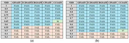
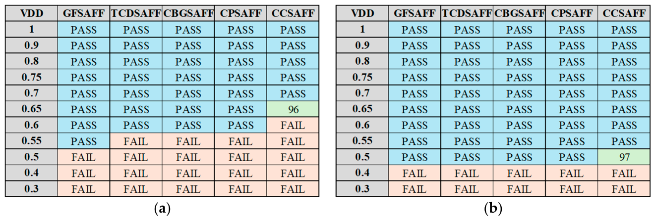
To assess operational stability, the flip-flop was evaluated under varying supply voltages. Figure 12a presents the results of 200 Monte Carlo simulations conducted with a 20 MHz clock under the SS corner at 125 °C. Figure 12b presents the corresponding results under the FF corner at −40 °C. Blue denotes a yield of more than 99%, whereas green denotes a yield of more than 95%. The proposed CCSAFF showed a yield of 96% at 0.65 V under the SS, 125 °C condition and 97% at 0.5 V under the FF, −40 °C condition. By comparison, conventional SAFF circuits showed yields above 99% at 0.6 V under the SS, 125 °C condition. This result suggests that CCSAFF has lower operational stability than conventional SAFF circuits. This is mainly due to the modified NOR gates that generate DBQ and DQB. In the low-voltage region, these gates require a longer time to generate valid logic levels. The transistor count of CCSAFF increased to 35, whereas that of the conventional GSSAFF was 24. However, the area penalty was held minimal because the number of stacked driver transistors in the latch stage was reduced. When the area of CCSAFF was normalized to 1, the relative areas of GFSAFF, TCDSAFF, CBGSAFF, and CPSAFF were figured to be 1.01, 1.07, 1.06, and 0.75, respectively. Enlarging the modified NOR gates can improve low-voltage operation, but it increases area overhead. Thus, a trade-off between low-voltage stability and area is necessary.
Figure 12.
Operability of flip-flops at scaled VDD obtained by 200 Monte-Carlo simulations: (a) SS corner, temperature 125 °C; (b) FF corner, temperature −40 °C.
Table 1 presents the overall performance comparison at 1.0 V and 1 GHz. The transistor count of CCSAFF is 35. The relative area of CCSAFF is normalized to 1, while those of CPSAFF and TCDSAFF are 0.75 and 1.07, respectively. Near-zero setup time is observed in all SAFF circuits except CPSAFF. The hold time of CCSAFF is 91.38 ps. The C-Q delay and D-Q delay are both 380 ps. Under the static condition without clock or data transitions, CCSAFF consumed 1.11 nW. Under switching activities of 0.01, 0.1, 0.5, and 1.0, the measured power consumptions were 27.4 uW, 32.7 uW, 55.2 uW, and 82.7 uW, respectively. The corresponding PDP values were 12.4 fWs, 21 fWs, and 31.4 fWs at switching activities of 0.1, 0.5, and 1.0, respectively. CCSAFF showed the lowest PDP among the circuits compared.
Table 1.
Comparison of various sense amplifier-based flip-flops at VDD = 1.0 V and fck = 1 GHz.
5. Discussion
CCSAFF achieves a favorable balance between timing performance and power efficiency, but this benefit is accompanied by reduced low-voltage operational stability. The area overhead is smaller than expected from the increased transistor count because the modified NOR gates use relatively small transistors as the number of stacked driver transistors in the latch stage is reduced. In contrast, CPSAFF shows the smallest area because its driver stage is controlled by a single SA output. The timing difference is also related to the circuit structure. In CPSAFF, the precharge operation depends on the comparison between D and Q, which requires a separate setup interval and results in a relatively long D-Q delay. By contrast, CCSAFF maintains a short D-Q delay with near-zero setup time. The power advantage of CCSAFF appears mainly during clocked operation. By suppressing redundant internal switching in the SA stage, it reduces power consumption under low-switching-activity conditions and shows the lowest PDP among the compared circuits. However, its low-voltage stability is limited by the small modified NOR gates. Therefore, further improvement of these gates is required, with careful consideration of the trade-off among area, power consumption, and D-Q delay.
6. Conclusions
A sense amplifier-based flip-flop circuit employing a conditional capture method to reduce energy consumption has been proposed. The proposed conditional capture sense amplifier-based flip-flop (CCSAFF) receives input signals through a modified NOR gate. The proposed circuit improves power consumption and D-Q delay characteristics despite the area increase caused by the addition of the modified NOR gate. The switching activity-based PDP results also confirm its high-power efficiency, particularly under low-switching-activity conditions. Therefore, the proposed circuit is a promising option for mobile applications with long standby periods and low-input-data activity. However, its practical application is limited by area overhead and degraded operational stability at low supply voltages. This limitation is mainly attributed to the reduced performance of the modified NOR gate under low-voltage conditions. Therefore, further optimization of the modified NOR gate structure is required to improve low-voltage operational stability and enhance its applicability as a viable component technology for future low-power systems.
Author Contributions
Conceptualization, C.L.; Methodology, C.L.; Validation, C.L.; Formal analysis, C.L.; Writing—original draft, C.L.; Writing—review & editing, H.Y.; Supervision, H.Y.; Project administration, H.Y. All authors have read and agreed to the published version of the manuscript.
Funding
This research received no external funding.
Data Availability Statement
The original contributions presented in this study are included in the article. Further inquiries can be directed to the corresponding author.
Acknowledgments
The EDA tool was supported by the IC Design Education Center (IDEC), Republic of Korea.
Conflicts of Interest
The authors declare no conflicts of interest.
References
- Anoop, D.; Nithin Kumar, Y.B.; Vasantha, M.H. High Performance Sense Amplifier Based Flip Flop for Driver Applications. In Proceedings of the 2017 IEEE International Symposium on Nanoelectronic and Information Systems (iNIS), Bhopal, India, 18–20 December 2017; pp. 129–132. [Google Scholar]
- Joo, B.; Kong, B.S. Low-Power High-Speed Sense-Amplifier-Based Flip-Flops With Conditional Bridging. IEEE Access 2023, 11, 121835–121844. [Google Scholar] [CrossRef] [Scilit]
- Hwang, H.C.; Kim, M.S.; Lee, D.S.; Kim, Y.G.; Kim, B.S.; Kang, K.H. An Area-Efficient True Single-Phase Clocked and Conditional Capture Flip-Flop for Ultra-Low-Power Operations in 7nm Fin-FET Process. In Proceedings of the 2024 IEEE Symposium on VLSI Technology and Circuits (VLSI Technology and Circuits), Honolulu, HI, USA, 16–20 June 2024; pp. 1–2. [Google Scholar]
- Joo, B.; Ko, M.; Lee, G.; Kong, B.S. A Single-Phase Contention- and Redundant Transition-Free Flip-Flop With Improved DQ Latency. IEEE J. Solid-State Circuits 2025, 60, 2249–2260. [Google Scholar] [CrossRef] [Scilit]
- Ko, M.; Joo, B.; Kong, B.S. A Low-Power Fully-Static Contention-Free Flip-Flop With Reduced Clock Load. IEEE Trans. Circuits Syst. II Express Briefs 2025, 72, 419–423. [Google Scholar] [CrossRef] [Scilit]
- Alioto, M.; Consoli, E.; Palumbo, G. Analysis and Comparison in the Energy-Delay-Area Domain of Nanometer CMOS Flip-Flops: Part I—Methodology and Design Strategies. IEEE Trans. Very Large Scale Integr. (VLSI) Syst. 2011, 19, 725–736. [Google Scholar] [CrossRef] [Scilit]
- Kim, J.C.; Jang, Y.C.; Park, H.J. CMOS sense amplifier-based flip-flop with two N-C2MOS output latches. Electron. Lett. 2000, 36, 498–500. [Google Scholar] [CrossRef] [Scilit]
- Khan, M.A.; Singh, M.K.; Upadhyay, A. A High-Speed Sense Amplifier Based Flip Flop with a Single Ended Latch Design and Low Voltage Operating Capabilities. In Proceedings of the 2023 3rd International Conference on Smart Generation Computing, Communication and Networking (SMART GENCON), Bangalore, India, 29–31 December 2023; pp. 1–7. [Google Scholar]
- Consoli, E.; Alioto, M.; Palumbo, G.; Rabaey, J. Conditional push-pull pulsed latches with 726fJ·ps energy-delay product in 65nm CMOS. In Proceedings of the 2012 IEEE International Solid-State Circuits Conference, San Francisco, CA, USA, 19–23 February 2012; pp. 482–484. [Google Scholar]
- Nikolic, B.; Oklobdzija, V.G.; Stojanovic, V.; Wenyan, J.; Chiu, J.; Leung, M. Improved sense-amplifier-based flip-flop: Design and measurements. IEEE J. Solid-State Circuits 2000, 35, 876–884. [Google Scholar] [CrossRef] [Scilit]
- Zhao, P.; Darwish, T.K.; Bayoumi, M.A. High-performance and low-power conditional discharge flip-flop. IEEE Trans. Very Large Scale Integr. (VLSI) Syst. 2004, 12, 477–484. [Google Scholar] [CrossRef] [Scilit]
- Teh, C.K.; Fujita, T.; Hara, H.; Hamada, M. A 77% energy-saving 22-transistor single-phase-clocking D-flip-flop with adaptive-coupling configuration in 40nm CMOS. In Proceedings of the 2011 IEEE International Solid-State Circuits Conference, San Francisco, CA, USA, 20–24 February 2011; pp. 338–340. [Google Scholar]
- Yao, M.; Zhang, X.; Chen, C.; Shen, L. Design of High-Speed and Low-Power Sense-Amplifier-Based Flip-Flop: Low redundancy flip-flop design. In Proceedings of the 2025 7th International Conference on Information Science, Electrical and Automation Engineering (ISEAE), Harbin, China, 18–20 April 2025; pp. 341–344. [Google Scholar]
- Okumura, T.; Hashimoto, M. Setup time, hold time and clock-to-Q delay computation under dynamic supply noise. In Proceedings of the IEEE Custom Integrated Circuits Conference 2010, San Jose, CA, USA, 19–22 September 2010; pp. 1–4. [Google Scholar]
- Strollo, A.G.M.; de Caro, D.; Napoli, E.; Petra, N. A novel high-speed sense-amplifier-based flip-flop. IEEE Trans. Very Large Scale Integr. (VLSI) Syst. 2005, 13, 1266–1274. [Google Scholar] [CrossRef] [Scilit]
- Kim, M.S.; Lee, H.; Park, J.S.; Kim, C.H.; Kang, J.; Shin, K.; Kagramanyan, E.; Jung, G.; Cho, U.; Shin, Y.; et al. Scan-controlled pulse flip-flops for mobile application processors. In Proceedings of the 2013 IEEE International Symposium on Circuits and Systems (ISCAS), Beijing, China, 19–23 May 2013; pp. 769–772. [Google Scholar]
- Shah, O.A.; Bansal, S.; Mavi, P.K.; Yadav, A.; Vats, S.; Ishrat, Z. Comparative Analysis of Dual-edge Triggered and Sense Amplifier Based Flip-flops in 32 nm CMOS Regime. In Proceedings of the 2023 International Conference in Advances in Power, Signal, and Information Technology (APSIT), Bhubaneswar, India, 9–11 June 2023; pp. 150–155. [Google Scholar]
- Nikolic, B.; Stojanovic, V.; Oklobdzija, V.G.; Wenyan, J.; Chiu, J.; Leung, M. Sense amplifier-based flip-flop. In Proceedings of the 1999 IEEE International Solid-State Circuits Conference, Digest of Technical Papers, ISSCC, First Edition (Cat. No. 99CH36278), San Francisco, CA, USA, 17 February 1999; pp. 282–283. [Google Scholar]
- Zhang, H.; Mazumder, P. Design of a new sense amplifier flip-flop with improved power-delay-product. In Proceedings of the 2005 IEEE International Symposium on Circuits and Systems (ISCAS), Kobe, Japan, 23–26 May 2005; Volume 1262, pp. 1262–1265. [Google Scholar]
- Kim, M.S.; Choi, W.; Kim, J.W.; Kim, C.; Oh, J.H.; Kong, B.S. Dynamic Differential Flip-Flop without Explicit Output Latching Stage for High-Speed SoC. In Proceedings of the 2021 28th IEEE International Conference on Electronics, Circuits, and Systems (ICECS), Dubai, United Arab Emirates, 28 November–1 December 2021; pp. 1–4. [Google Scholar]
- Shah, O.A.; Nijhawan, G.; Khan, I.A. Improved Sense Amplifier Based Flip Flop Design for Low Power And High Data Activity Circuits. J. Appl. Sci. Eng. 2022, 26, 1047–1053. [Google Scholar] [CrossRef]
- Yuan, A.; Zhao, H.; Li, Z.; Qiao, S. A novel high-speed low-power sense-amplifier-based flip-flop for digital circuits application. IEICE Electron. Express 2023, 20, 20230446. [Google Scholar] [CrossRef] [Scilit]
- Lin, J.F.; Hwang, Y.T.; Wong, C.S.; Sheu, M.H. Single-ended structure sense-amplifier-based flip-flop for low-power systems. Electron. Lett. 2015, 51, 20–21. [Google Scholar] [CrossRef] [Scilit]
- Jeong, H.; Oh, T.W.; Song, S.C.; Jung, S.O. Sense-Amplifier-Based Flip-Flop With Transition Completion Detection for Low-Voltage Operation. IEEE Trans. Very Large Scale Integr. (VLSI) Syst. 2018, 26, 609–620. [Google Scholar] [CrossRef] [Scilit]
- Zhao, X.; Li, Z.; Liu, J.; Li, L.; Zhao, Y.; Zhao, H.; Qiao, S. Low-power non-redundant transition sense amplifier based flip-flops with conditional pre-charge and completion detection. IEICE Electron. Express 2026, 23, 20250431. [Google Scholar] [CrossRef] [Scilit]

Disclaimer/Publisher’s Note: The statements, opinions and data contained in all publications are solely those of the individual author(s) and contributor(s) and not of MDPI and/or the editor(s). MDPI and/or the editor(s) disclaim responsibility for any injury to people or property resulting from any ideas, methods, instructions or products referred to in the content. |
© 2026 by the authors. Licensee MDPI, Basel, Switzerland. This article is an open access article distributed under the terms and conditions of the Creative Commons Attribution (CC BY) license.