


Abstract
In high-bandwidth memory (HBM) testing through the direct access (DA) port, the response-path bandwidth is far lower than the internal data bandwidth. Because most read responses are fault-free, transferring every response incurs substantial transfer overhead and test time. This paper proposes three fault-data transfer methods. Selective staggered read suppresses fault-free response transfers and overlaps faulty-response transfers with the subsequent read latency. Duplicate fault suppression replaces identical fault responses at consecutive addresses with a short duplicate code. Failing-bit indexing transmits only the positions of failing bits. The proposed architecture controls whether, when, and in which format each response is transferred without modifying the DA port interface or the March command and address sequence. Cycle-accurate simulation of an HBM2 test model shows that, across Random, Column-Correlated, and Row-Correlated Fault models with fault rates of 0.01–5%, the proposed method reduces the DA response data by 99.32–99.99% and the total test time by 44.86–45.01% compared with the conventional method. Synthesis shows that the added logic is smaller than that of on-chip fault collection and signature compaction schemes and independent of the memory capacity. The proposed architecture attains nearly the same test time as on-chip fault collection and signature compaction schemes while delivering every faulty response and its failing-bit positions to the tester, so that its diagnostic coverage is not bounded by on-chip storage.
1. Introduction
Recent advances in artificial intelligence, high-performance computing, and massively parallel computing systems have rapidly increased the demand for memory bandwidth [1,2]. To meet this demand, high-bandwidth memory (HBM) vertically stacks multiple dynamic random-access memory (DRAM) dies and interconnects them using through-silicon vias (TSVs), thereby providing both high data bandwidth and high integration density [3,4]. Compared with conventional single-die DRAM, however, HBM has a considerably more complex architecture that includes a vertically stacked structure, a wide I/O interface, a silicon-interposer-based package, and multiple internal channels. These structural characteristics make post-manufacturing test access and fault analysis more challenging [5]. Accordingly, test methods that achieve both high test quality and high test efficiency have become increasingly important for HBM [6,7,8].
Memory testing is generally classified into built-in self-test (BIST), which employs on-chip test circuitry, and external testing based on automatic test equipment (ATE). BIST integrates test-pattern generation, response comparison, and pass/fail decision functions within the memory, thereby enabling high-speed testing while minimizing external data transfer [9,10]. However, BIST offers relatively limited flexibility in modifying test algorithms and in collecting the detailed diagnostic information required for fault analysis. On-chip schemes that collect fault addresses in content-addressable memories for built-in self-repair (BISR) [7,8] or compact test responses into signatures for offline diagnosis avoid the transfer of responses, but the amount of fault information they can retain is bounded by the on-chip storage. These limitations are particularly significant for HBM, whose stacked architecture and multiple internal channels demand detailed diagnostic information such as fault locations, fault patterns, and fault recurrence characteristics. Flexible test control and detailed fault analysis using an external ATE therefore play an essential role in HBM testing.
For ATE-based test access, HBM provides a direct access (DA) port [11]. In DA-based testing, the ATE applies commands and addresses to control the test operations and collects fault information from the read responses or the internal comparison results [12]. This approach allows test patterns and address sequences to be controlled flexibly from outside the memory and gives the ATE direct access to the information required for fault analysis. However, the DA port provides substantially lower physical bandwidth than the functional HBM data I/O path. Because the DA interface must also carry control and status information, the resources available for transferring actual fault data are even more limited. Owing to the wide data width and large capacity of HBM, transmitting every read response or comparison result through this bandwidth-limited test path incurs considerable transfer overhead. Moreover, most addresses produce fault-free responses during testing, yet the conventional fixed-timing transfer method transmits every response regardless of whether it contains a fault. As a result, fault-free response data that are unnecessary for fault analysis occupy the DA path, aggravating the transfer bottleneck and increasing both the storage requirements and the post-processing workload of the ATE. Despite the flexibility of DA-based testing, the limited response bandwidth is thus a major contributor to the overall test time and test cost. To alleviate this data-transfer bottleneck, this paper proposes a fault-data transfer architecture for DA-based HBM testing that adaptively controls whether, when, and in which format a read response is transferred according to the internal comparison result, while preserving the existing DA-port interface and the command and address sequence of the March algorithm. The architecture comprises three complementary methods that target fault-free responses, repeated fault responses, and sparse fault responses, respectively.
The main contributions of this paper are summarized as follows.
- Selective staggered read suppresses the external transfer of responses that the internal comparison circuitry identifies as fault-free and overlaps the transfer of a faulty response with the read-latency interval of the subsequent read operation, thereby eliminating unnecessary transfers and reducing the additional cycles required for fault-data transfer.
- Duplicate fault suppression transmits a complete fault response only for its first occurrence and replaces identical responses at consecutive addresses with a short duplicate code, thereby eliminating repeated transfers of identical fault data.
- Failing-bit indexing transmits only the positions of failing bits as 7-bit index codes rather than the entire fault-data word, thereby reducing the amount of information required to represent sparse faults.
- The proposed methods are evaluated with a cycle-accurate C-based HBM2 test model under Random, Column-Correlated, and Row-Correlated Fault models. At a 5% random fault rate, the proposed method reduces the DA response data by 99.32% and the total test time by 44.86% compared with the conventional method. Across the three fault models with fault rates of 0.01–5%, it achieves response-data reductions of 99.32–99.99% and test time reductions of 44.86–45.01%.
- The hardware overhead, test time, and diagnostic coverage of the proposed architecture are compared with those of the conventional DA transfer, CAM-based fault collection, and signature-based compaction under the same memory organization.
The remainder of this paper is organized as follows. Section 2 reviews related work on HBM testing, on-chip fault-data handling, and the DA-based test architecture. Section 3 describes the proposed fault-data transfer architecture and the operating principles of the three methods. Section 4 presents the evaluation results and the comparison with the existing schemes, and Section 5 concludes the paper.
2. Related Work
Memory-cell testing commonly employs March algorithms, such as March C−, in which read and write operations are applied repeatedly over the entire address space and the result of each read operation is determined by comparing the read data with the expected value [13]. Effective HBM testing therefore requires not only an architecture that can efficiently control a large number of memory operations but also a mechanism for observing the responses or comparison results generated by those operations. Because HBM features a wide data interface and a large memory capacity, dedicated architectural support is essential for an efficient test environment.
To provide such control and observation capabilities on-chip, programmable BIST architectures have been studied in which test commands, addresses, and data are generated internally and read responses are compared with the expected values within the memory [9,10]. By configuring the associated control information, programmable BIST can flexibly support various March algorithms and construct test sequences tailored to the memory organization and the target fault models. In addition, because both test execution and response evaluation are performed on-chip, the control burden on the external ATE is reduced, and the functional status of the memory can be determined without transferring large volumes of raw read data off-chip.
Because programmable BIST evaluates read responses on-chip, the pass/fail decision requires no off-chip transfer of response data. However, the information required for fault analysis, namely the locations, patterns, and recurrence characteristics of the faults detected at individual addresses, exceeds the limited on-chip storage, so programmable BIST retains only a small portion of it. Its applicability is thus limited to test flows in which a pass/fail decision is sufficient. This limitation is particularly critical for HBM, whose stacked architecture and wide internal data path require analysis beyond simple pass/fail determination. Analyzing the spatial distribution and recurrence characteristics of faults requires external access to the detailed responses and internal comparison results of individual read operations. Consequently, programmable BIST must be complemented by a DA-based test-access architecture in which the ATE applies test commands and data through the DA port and directly observes the resulting read responses or internal comparison results.
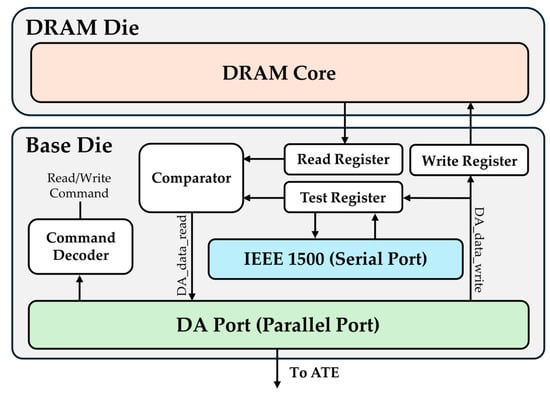
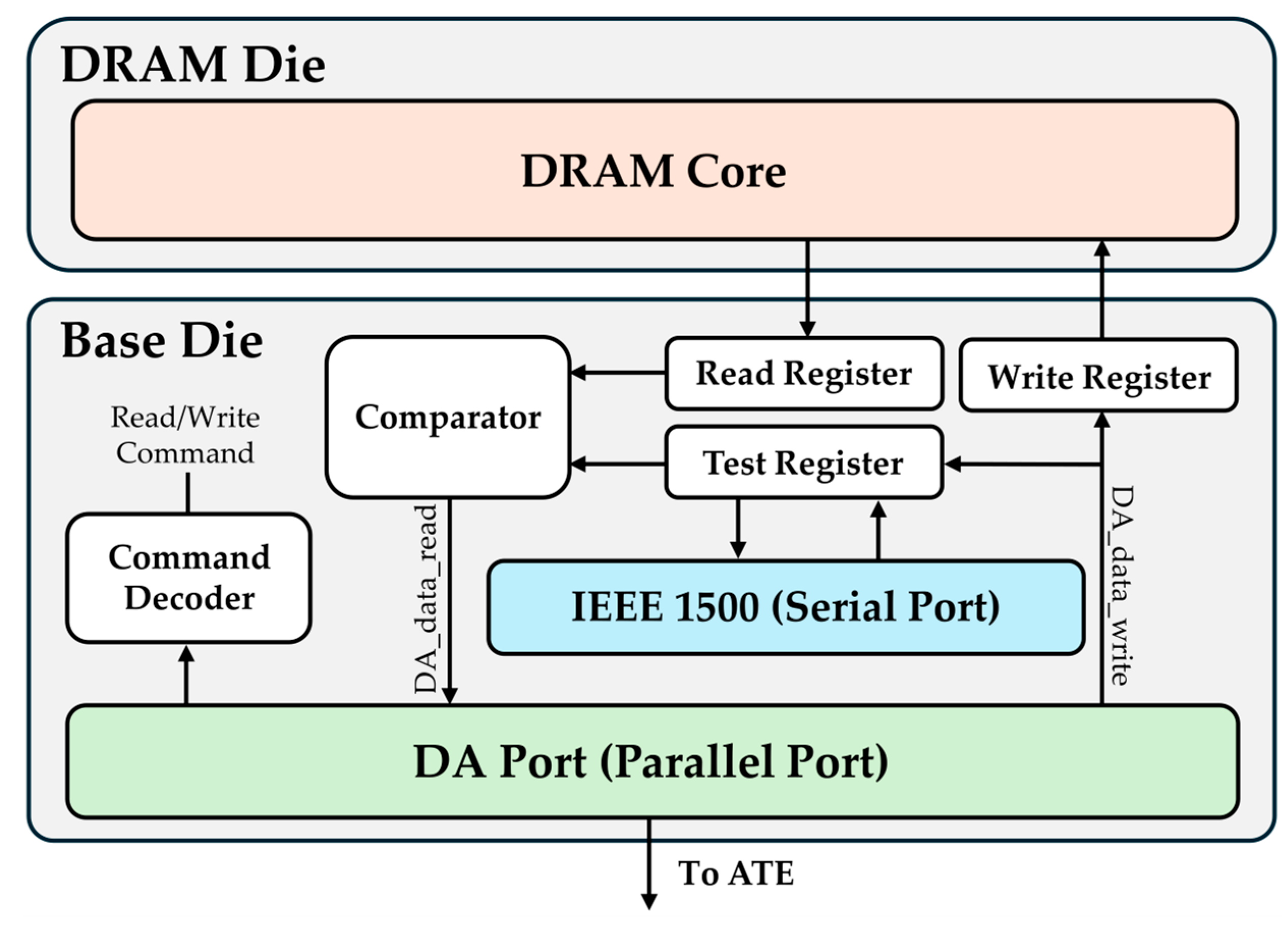
To provide such external test access, Lee et al. [12] proposed the DA-based HBM test architecture shown in Figure 1. In this architecture, an external ATE applies test commands and data through the DA port implemented in the HBM base die and retrieves the read responses of the memory cells and the internal comparison results. Test commands supplied through the DA port are decoded by the command decoder, write data are delivered to the DRAM core through the write register, and the data read from the memory cells are captured in the read register. The on-chip comparator compares the read data with the expected data held in the test register, and the comparison result is returned to the ATE through the bandwidth-limited DA response path, DA_data_read. An IEEE 1500-based serial port serves as an auxiliary path for loading the test register and for additional test control and observation [12,14]. The DA mode is defined in the HBM3 standard [15], and the challenges of testing HBM through such access paths have been surveyed in [16].
Figure 1.
DA-based HBM test architecture.
Although the DA-based test architecture provides direct test access to the memory cells and improves the observability of test responses, retrieving the response information externally incurs substantial transfer overhead. The response or comparison result of every read operation is transferred through the bandwidth-limited DA response path at a fixed timing, regardless of whether it contains a fault, so the data-transfer burden accumulates as testing proceeds. Moreover, because faults generally occur only sparsely over the address space, most of the transferred information is fault-free and unnecessary for fault analysis, yet it repeatedly occupies the available transfer resources. As a result, both the total test time and the amount of transferred data increase, while the utilization of the limited test path decreases. This problem is further aggravated by the bandwidth disparity between the high-speed internal HBM data path and the relatively narrow DA test port. Therefore, the transfer efficiency of the information delivered through the bandwidth-limited DA response path must be improved while preserving the test accessibility and fault observability of conventional DA-based HBM testing.
One way to avoid the transfer of read responses is to keep the fault information on-chip and to process it there. BISR and built-in redundancy analysis schemes collect the addresses of the detected faults in content-addressable memories (CAMs) and determine the spare allocation on-chip [7,8,17,18,19]. In the scheme of Yoon et al. [8], a fault whose row and column addresses differ from those of every stored fault is recorded in an address CAM, a fault that shares a row or a column with a stored fault is recorded in a hybrid CAM, and the number of entries of the two CAMs is determined by the number of spare rows and spare columns. Fault collection and repair analysis proceed concurrently with the test, so that the repair solution is available without additional analysis cycles when the test ends. Han et al. [17] place a common spare on the base die that is shared by all stacked dies, which raises the repair rate of 3D memory for the same hardware overhead, and Kim et al. [7] reduce the area of the fault address memory of HBM BISR with a hybrid memory structure. Earlier CAM-based analyzers exploit the characteristics of pivot faults to reduce the analysis hardware [18] and perform the analysis dynamically while the test is running [19]. Because these schemes serve repair rather than diagnosis, only the fault addresses are retained, and fault collection ends when the CAM entries are exhausted, after which the memory is classified as unrepairable.
Signature-based diagnosis retains the fault information in a different form. Mukherjee et al. [20,21] compact the comparator outputs at system speed into a fixed set of registers, which consist of a signature register driven by a multiple-input ring generator, a failing-word counter, and failing-row and failing-column indicators, and download the registers after each March element without interrupting the test. The error bitmap is then reconstructed offline from the downloaded values and reference signatures. Related schemes compress the diagnostic data of each faulty word on-chip before exporting them [22] or apply convolutional compaction to the diagnosis of emerging memories [23]. The amount of retained information is fixed by the register lengths regardless of the number of faults, so that the fault set can be identified only while it lies within the resolution of the signature. A programmable BIST with a diagnosis result memory stores the address and data of each mismatch without compression and suspends the test to dump the memory when it is full [24]. In all of these on-chip schemes, the number of faults that can be analyzed is bounded by the size of the on-chip storage, whereas DA-based testing delivers the fault information itself to the ATE and leaves its storage and analysis to the ATE.
Recent memory-test studies have reduced the external test-data and fail-data overhead by minimizing the number of ATE pins, reducing the output data, compressing the fail-address information, and selectively collecting the data required for redundancy analysis [25,26,27,28]. These approaches reduce the ATE resources needed to receive, store, and process the fail information after it has left the chip, rather than the volume of test responses that cross the bandwidth-limited DA path of HBM.
Programmable BIST, CAM-based fault collection, and signature-based compaction avoid transferring responses, but the fault information they retain is bounded by on-chip storage. The conventional DA-based architecture delivers the fault information itself to the ATE but transfers every response regardless of its content. None of the previous approaches reduces the volume of responses that cross the bandwidth-limited DA path while preserving the fault information delivered to the ATE. The fault-data transfer architecture proposed in this paper reduces the response volume on the DA path itself. The architecture preserves the DA-port interface and the command and address sequence of the March algorithm and transfers only the faulty responses, in a compact form and as soon as they are detected, so that no on-chip fault storage is required and the number of faults that can be analyzed is not limited by the storage capacity. Section 3 describes the three methods that implement the architecture, and Section 4 compares its hardware overhead, test time, and diagnostic coverage with those of the existing schemes.
3. Proposed Method
This section presents a fault-data transfer architecture that preserves the DA-port-based command and address input and response observation while adaptively controlling whether, when, and in which format fault information is transferred according to the internal comparison results. The proposed architecture consists of three methods: selective staggered read, duplicate fault suppression, and failing-bit indexing.
3.1. Selective Staggered Read
In DA-based HBM testing, all read responses are transferred through the bandwidth-limited DA response path regardless of whether faults are present. In this work, the test data width is 128 bits, and each read response is therefore transferred as a 128-bit word. Consequently, the repeated transfer of 128-bit fault-free responses, which constitute the majority of test responses, becomes a major source of additional test time. To address this issue, we propose a selective staggered read method that transfers only the responses in which a fault is detected and retains each selected response until the subsequent read command is issued. For fault-free responses, no valid output interval is generated, thereby eliminating unnecessary transfers. For faulty responses, the transfer is overlapped with the read latency (RL) interval of the subsequent read operation, which minimizes the additional cycles required for fault-data transfer.
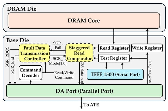
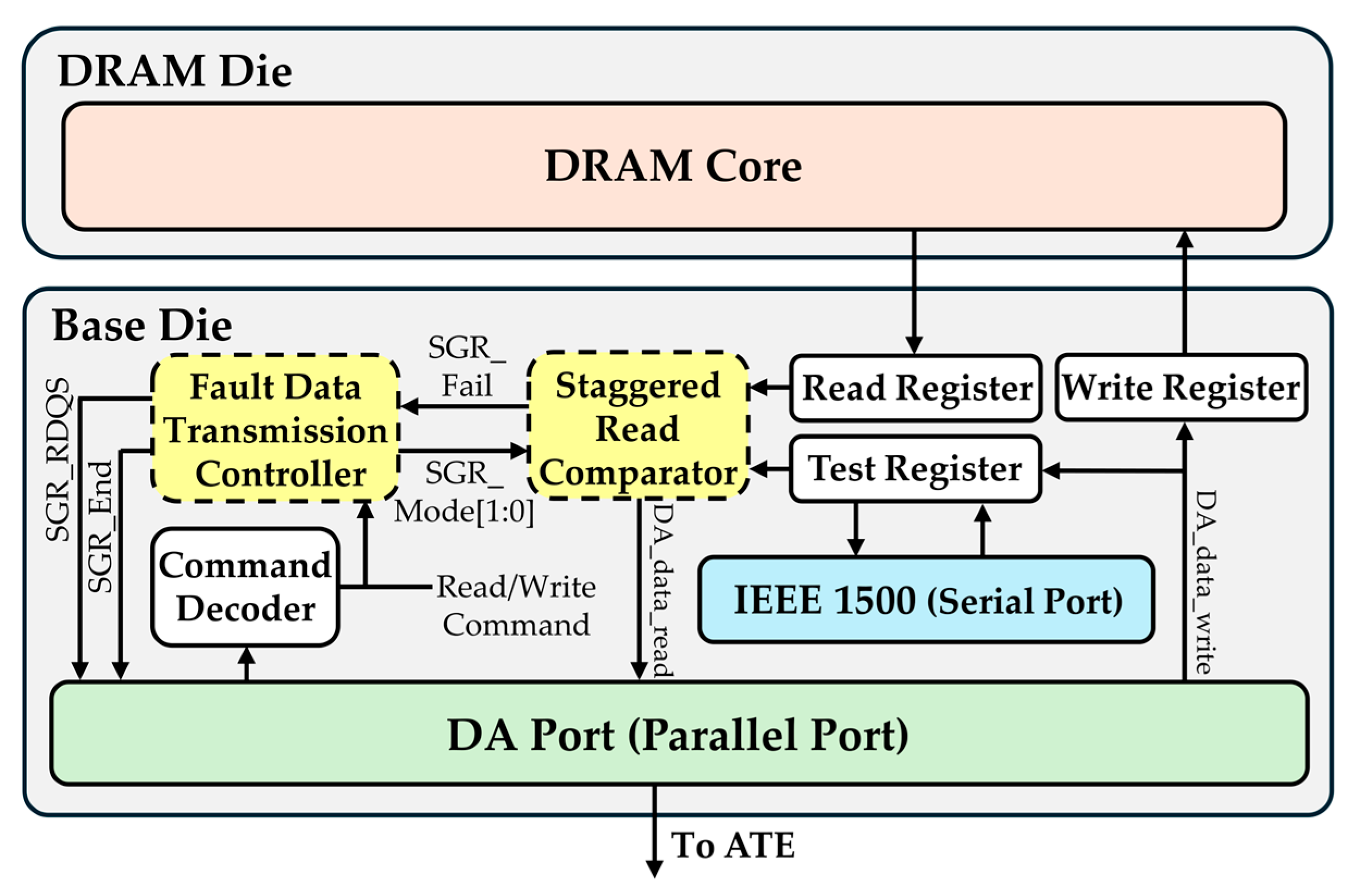
Figure 2 illustrates the control and data paths for the selective staggered read operation. The proposed architecture consists of a staggered read comparator, which performs bitwise comparison between the read data and the expected data and stores the resulting fault data, and a Fault Data Transmission Controller, which manages the storage state and transmission timing of the generated fault data. The Read Register and Test Register store the 128-bit data read from the memory cells and the corresponding expected data, respectively, and provide them as inputs to the staggered read comparator. The comparator stores the bitwise comparison results in its internal Result Register and generates SGR_Fail. The Fault Data Transmission Controller receives the read command from the command decoder together with SGR_Fail and generates SGR_Mode[1:0], SGR_RDQS, and SGR_End. SGR_Fail indicates whether the current read response contains at least one mismatch between the read data and the expected data. SGR_Mode[1:0] is a 2-bit control signal that determines the operation of the Result Registers: 2′b10 loads the comparison results, 2′b01 retains the stored fault data, and 2′b00 enables serial shifting of the stored fault data. SGR_RDQS serves as the read strobe of the DA response path. Analogous to the data strobe (DQS) of a conventional DRAM interface, it indicates that the read data transferred from the HBM to the ATE are valid while it is asserted. SGR_End is asserted when the transmission of the fault data associated with a read response is completed, so that the ATE can identify the end of each transferred response. Among these signals, SGR_Mode controls the comparator internally, whereas SGR_RDQS and SGR_End are delivered to the ATE through the DA port.
Figure 2.
Control and data paths for selective staggered read.
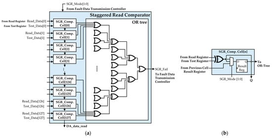
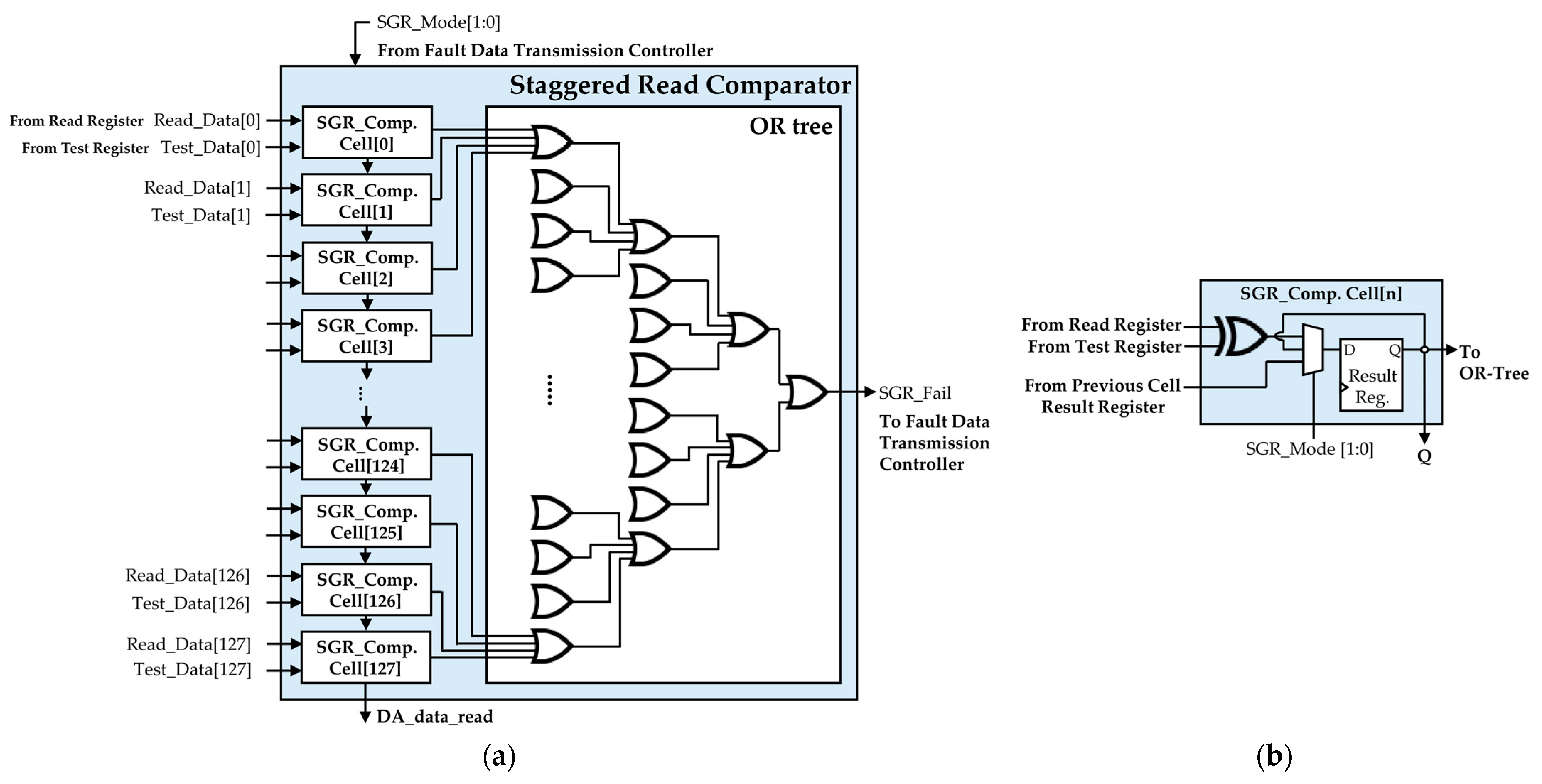
The detailed structure of the staggered read comparator is shown in Figure 3a. It consists of 128 comparison cells and an OR tree. Each cell corresponds to one bit of the 128-bit HBM data width, and the OR tree combines the fault bits generated by the individual cells. As shown in Figure 3b, each comparison cell receives the corresponding bits from the Read Register and Test Register and performs a bitwise XOR operation. The XOR output and the output of the Result Register in the preceding comparison cell are connected to a multiplexer controlled by SGR_Mode[1:0], and the selected value is stored in the Result Register. This structure enables each Result Register to store the comparison result during fault detection and to form a serial shift path during fault-data transmission. The fault bit Fi generated by the ith comparison cell is defined by Equation (1), where Ri and Ti denote the ith bits provided by the Read Register and Test Register, respectively.
Fi = Ri⊕Ti
Figure 3.
Structure of the staggered read comparator: (a) overall architecture of the 128-bit comparator and (b) detailed structure of an individual comparison cell.
If Ri = Ti, then Fi = 0, indicating a fault-free bit. Otherwise, Fi = 1, indicating a mismatch at the corresponding bit position. The fault bits stored in the Result Registers of all comparison cells are fed in parallel to the OR tree. Accordingly, SGR_Fail, which indicates whether the entire read response contains a fault, is defined by Equation (2). Thus, SGR_Fail is asserted when at least one of the 128 bits contains a mismatch and remains deasserted when all bits match. During fault-data transmission, the Result Registers operate as a serial shift chain, and the Q output of the final comparison cell, SGR_Comp_Cell[127], is transferred through DA_data_read. Once SGR_Fail is asserted, the Fault Data Transmission Controller manages the retention and transmission state of the corresponding fault response.
Algorithm 1 summarizes the operation of the selective staggered read method. When a read command and address are applied, the Fault Data Transmission Controller sets SGR_Mode to 2′b10, and the bitwise XOR results generated by the staggered read comparator are loaded into the corresponding Result Registers. The Result Register outputs are then combined through the OR tree to generate SGR_Fail, which the controller uses to determine whether the current read response contains at least one mismatch. When SGR_Fail = 0, the response is classified as fault-free. In this case, SGR_RDQS remains deasserted, and the test proceeds to the next read operation without generating a valid output interval on the bandwidth-limited DA response path. Consequently, the 128-bit comparison result of a fault-free response is not transferred to the ATE, and the serial-transfer cycles that would otherwise be required are eliminated. When SGR_Fail = 1, the fault data stored in the Result Register are not transmitted immediately. Instead, they are retained with SGR_Mode = 2′b01 until the next read command is issued. Upon arrival of the subsequent read command, the Fault Data Transmission Controller changes SGR_Mode to 2′b00 and asserts SGR_RDQS. The fault data from the previous address are then serially shifted out of the Result Register and transferred through the bandwidth-limited DA response path. At the same time, the read operation for the newly applied address proceeds in parallel. After the transmission of the previous fault data is completed, SGR_RDQS is deasserted, SGR_End is asserted, and SGR_Mode returns to 2′b01. The comparison result for the newly applied address is then loaded into the Result Register by setting SGR_Mode to 2′b10, and the same fault-detection and transfer procedure is repeated. In this manner, the proposed architecture overlaps fault-data transmission from the previous address with the processing of the subsequent read operation instead of executing these operations sequentially.
| Algorithm 1: Selective Staggered Read Operation | |
| 1: | procedure SELECTIVE_STAGGERED_READ |
| 2: | Enter DA test mode |
| 3: | Apply read command and address |
| 4: | while test operation is not completed do |
| 5: | SGR_Mode ← 2′b10 |
| 6: | for n ← 0 to 127 do |
| 7: | Result_Reg[n] ← Read_Data[n] ⊕ Test_Data[n] |
| 8: | end for |
| 9: | SGR_Fail ← OR(Result_Reg) |
| 10: | if SGR_Fail = 0 then |
| 11: | SGR_RDQS ← 0 |
| 12: | Apply next read command and address |
| 13: | else |
| 14: | SGR_Mode ← 2′b01 |
| 15: | Hold Result_Reg |
| 16: | Wait until the next read command is issued |
| 17: | SGR_Mode ← 2′b00 |
| 18: | SGR_RDQS ← 1 |
| 19: | for n ← 127 downto 0 do |
| 20: | DA_data_read ← Result_Reg[127] |
| 21: | Shift Result_Reg |
| 22: | end for |
| 23: | SGR_RDQS ← 0 |
| 24: | SGR_End ← 1 |
| 25: | SGR_Mode ← 2′b01 |
| 26: | end if |
| 27: | end while |
| 28: | end procedure |
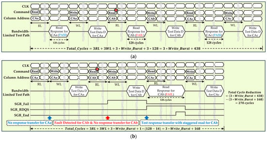
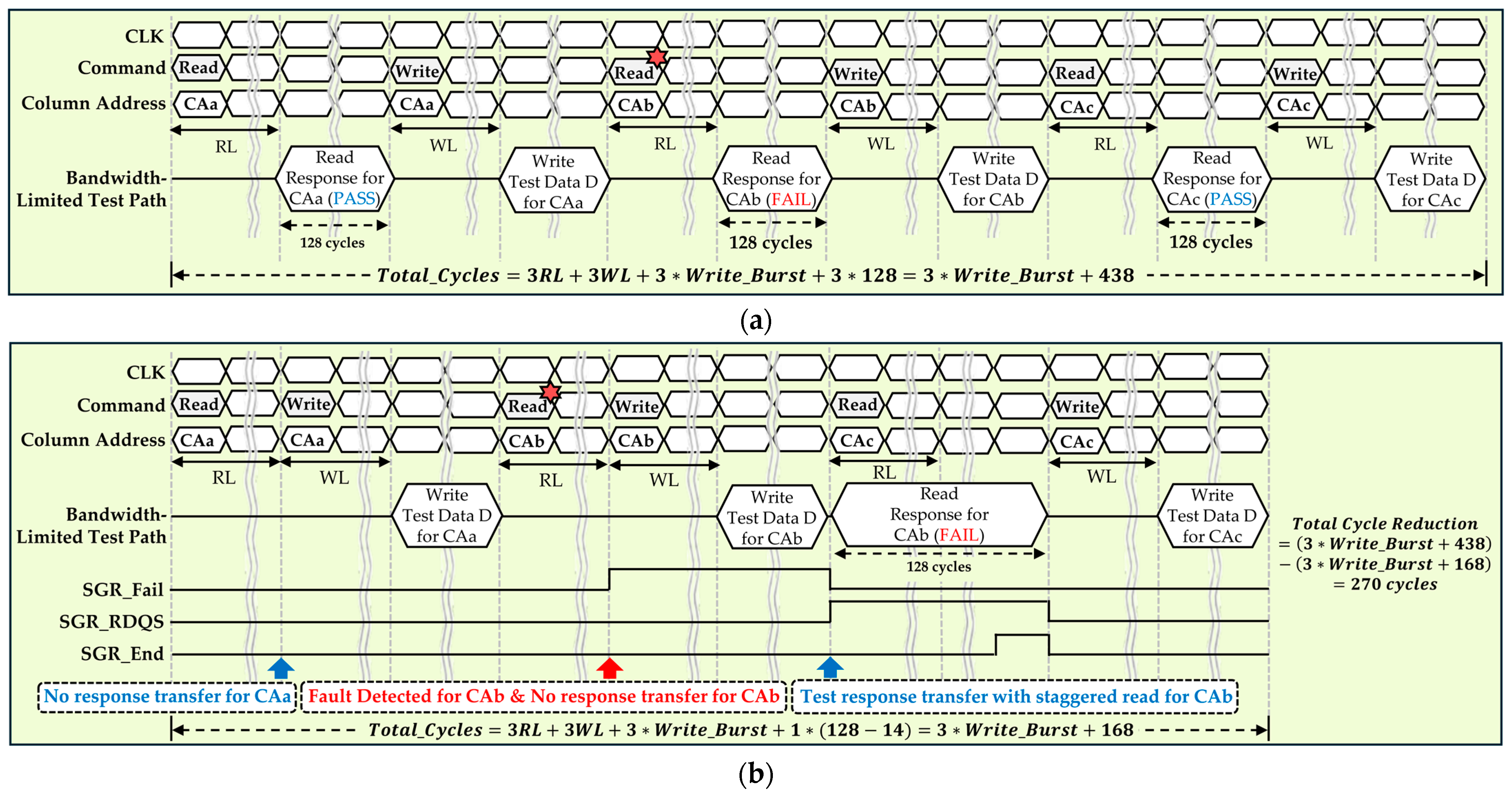
Figure 4 compares the response-transfer timing of the conventional method and the proposed selective staggered read method for three consecutive read operations at addresses CAa, CAb, and CAc. In this example, RL and the write latency (WL) are set to 14 and 4 cycles, respectively. The read responses at CAa and CAc are assumed to be fault-free, whereas a fault is detected in the response at CAb. Because the bandwidth-limited test path is one bit wide, transmitting a complete 128-bit read response requires 128 serial-transfer cycles. The transfers of write test data shown in the figure are common to both methods and are therefore represented by Write_Burst without a specific transfer length. In the conventional method shown in Figure 4a, every 128-bit read response is transferred immediately after RL regardless of whether the response is fault-free or faulty. Consequently, the responses at CAa, CAb, and CAc require a total of 3 × 128 = 384 response-transfer cycles, and the total cycle count is expressed as 3RL + 3WL + 3 Write_Burst + 3 × 128. In contrast, the proposed method shown in Figure 4b suppresses the response transfers at CAa and CAc because both responses are fault-free.
Figure 4.
Comparison of response-transfer timing: (a) conventional DA-based response transfer and (b) response transfer using the selective staggered read method.
When a fault is detected at CAb, SGR_Fail is asserted and remains high, and the CAb fault response is retained in the Result Registers instead of being transmitted immediately. When the subsequent read command for CAc is issued, the retained CAb fault response is serially transmitted. During this transfer, SGR_RDQS remains asserted to indicate that valid fault data are present on the bandwidth-limited test path. Because the first 14 cycles of the 128-bit CAb fault-response transfer overlap with the RL interval of the CAc read operation, only the remaining 128 − 14 = 114 cycles contribute additional response-transfer time. After the final fault-data bit is transferred, SGR_RDQS is deasserted and SGR_End is asserted to indicate completion of the response transfer. Therefore, for the three read operations shown in Figure 4, the proposed method reduces the transferred response data from 384 bits to 128 bits, corresponding to a 66.7% reduction. The response-transfer overhead is reduced from 384 serial-transfer cycles in the conventional method to 114 additional cycles in the proposed method, yielding a reduction of 270 response-transfer cycles. Because the transfers of write test data and their timing are identical in both methods, they do not affect this reduction. In general, if the length of a selected fault response does not exceed RL, its entire transfer can be hidden within the RL interval of the subsequent read operation; otherwise, only the portion exceeding RL contributes additional transfer cycles.
3.2. Duplicate Fault Suppression
The selective staggered read method presented in Section 3.1 suppresses the transfer of fault-free responses. However, faulty responses must still be transferred externally. For faults associated with wordlines or bitlines, identical fault data may occur repeatedly at consecutively accessed addresses, depending on the address sequence of the test. Transmitting all such responses results in repeated serial-transfer cycles even though they provide no new fault information. To address this issue, we propose a duplicate fault suppression method that transmits the complete fault response only for the first occurrence and replaces subsequent identical responses at consecutive addresses with a short code that indicates duplication.
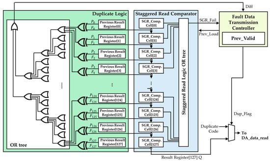
Figure 5 illustrates the hardware architecture for duplicate fault suppression. Rather than introducing a separate controller, the proposed architecture extends the Fault Data Transmission Controller described in Section 3.1 with functions for duplicate detection, storage of the previous fault data, and output selection. The 128-bit fault data of the current address are stored in the Result Registers of the staggered read comparator, and an additional Previous Result Register preserves the representative fault data of the preceding address. Duplicate detection is performed before the Previous Result Register is updated. The current and previous fault data are compared bit by bit using 128 XOR operations, and the resulting comparison bits are combined through an OR tree to generate a single Diff signal. Let Fi and Pi denote the ith bits of the Result Register and the Previous Result Register, respectively. Then, Diff is defined by Equation (3).
Figure 5.
Comparison and output-selection architecture for duplicate fault suppression.
When the current and previous fault-data words are identical, Diff = 0. When at least one bit position differs, Diff = 1. However, Diff indicates only whether the two register contents are identical, not whether the value stored in the Previous Result Register is a valid fault response of the immediately preceding address. To distinguish these cases, the Fault Data Transmission Controller maintains an internal state signal, Prev_Valid, which records whether the immediately preceding address produced a valid fault response. The controller classifies the current response as a consecutive duplicate only when Prev_Valid = 1 and Diff = 0. For a nonduplicate faulty response, Prev_Load is asserted to store the current Result Register contents in the Previous Result Register, Prev_Valid is set to 1, and Dup_Flag is cleared to 0. For a duplicate faulty response, the Previous Result Register is retained, Prev_Valid remains 1, and Dup_Flag is set to 1. In contrast, a fault-free response resets Prev_Valid and Dup_Flag to 0 without updating the Previous Result Register. This mechanism prevents identical fault data separated by a fault-free address from being incorrectly classified as consecutive duplicates.
Algorithm 2 summarizes the operation of the duplicate fault suppression method. After the current comparison result is stored in the Result Register, the Fault Data Transmission Controller first evaluates SGR_Fail. When SGR_Fail = 0, the current response is classified as fault-free, and its external transfer is suppressed according to the selective staggered read method described in Section 3.1. At the same time, Prev_Valid and Dup_Flag are reset to 0, terminating any sequence of consecutive duplicate fault responses before the next read operation proceeds. When SGR_Fail = 1, the controller compares the current Result Register with the Previous Result Register to generate Diff and evaluates it together with Prev_Valid. If Prev_Valid = 1 and Diff = 0, the current fault response is identical to that of the immediately preceding address and is therefore classified as a duplicate fault. In this case, the Previous Result Register is retained, Prev_Valid remains asserted, and Dup_Flag is set to 1. The output MUX then selects the Duplicate Code instead of the complete fault data for subsequent transmission. If Prev_Valid = 0 or Diff = 1, the current response is classified as a nonduplicate fault. The current Result Register contents are then stored in the Previous Result Register, Prev_Valid is set to 1, and Dup_Flag is cleared to 0. The output MUX selects the Result Register contents as the representative fault data for transmission. In both cases, the selected response is subsequently transferred according to the staggered transmission procedure described in Section 3.1.
| Algorithm 2: Duplicate Fault Suppression Operation | |
| 1: | procedure DUPLICATE_FAULT_SUPPRESSION |
| 2: | Store current comparison result in Result_Reg |
| 3: | if SGR_Fail = 0 then |
| 4: | Prev_Valid ← 0 |
| 5: | Dup_Flag ← 0 |
| 6: | Proceed to next read operation |
| 7: | else |
| 8: | Diff ← OR(Result_Reg ⊕ Previous_Result_Reg) |
| 9: | if Prev_Valid = 1 and Diff = 0 then |
| 10: | Retain Previous_Result_Reg |
| 11: | Prev_Valid ← 1 |
| 12: | Dup_Flag ← 1 |
| 13: | Select Duplicate_Code for transmission |
| 14: | else |
| 15: | Previous_Result_Reg ← Result_Reg |
| 16: | Prev_Valid ← 1 |
| 17: | Dup_Flag ← 0 |
| 18: | Select Result_Reg for transmission |
| 19: | end if |
| 20: | Proceed to next read operation |
| 21: | end if |
| 22: | end procedure |
The Duplicate Code indicates that the fault pattern of the current address is identical to that of the immediately preceding address. Upon receiving this code, the ATE does not need to receive another 128-bit fault-data word for the current address; instead, it reuses the most recently received representative fault data as the fault pattern of the current address. Therefore, when identical fault data occur over multiple consecutive addresses, the complete fault data are transferred only for the first address, whereas only the Duplicate Code is transmitted for the subsequent addresses. The ATE can thereby reconstruct the fault information associated with each address. Consequently, duplicate fault suppression eliminates repeated transfers of identical fault responses over consecutive address ranges, reducing both the amount of data transferred through the DA path and the required serial-transfer cycles.
3.3. Failing-Bit Indexing
The duplicate fault suppression method presented in Section 3.2 replaces repeated fault responses with a Duplicate Code when identical fault data occur at consecutive addresses. However, a nonduplicate faulty response is still transferred as the original 128-bit fault-data word. When only a few bits are faulty, most of the word consists of fault-free zeros, which are transmitted together with the actual fault information. To reduce this overhead, we propose a failing-bit indexing method that encodes the positions of the failing bits of a nonduplicate faulty response as 7-bit index codes and transmits only these codes.
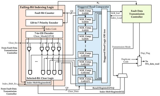
Figure 6 shows the overall architecture for failing-bit indexing and transmission-format selection. The 128-bit fault data stored in the Result Registers of the staggered read comparator are supplied to the Failing-Bit Indexing Logic under the control of Index_Load, which is generated by the Fault Data Transmission Controller. When Index_Load is asserted, the current 128-bit fault data are provided in parallel to the Fault Bit Counter and the 128-to-7 Priority Encoder. The Fault Bit Counter determines the number of failing bits, denoted by NF, and provides this value to the Fault Data Transmission Controller. Based on NF, the controller determines the transmission format and generates the control signals required for selected-bit clearing, serial index transmission, and output selection. Clear_En enables the Selected-Bit Clear Logic to clear the failing bit selected by the 7-to-128 Decoder, while Index_Shift_En controls the serial shifting of the 7-bit index stored in the Index Shift Register. Transmission_Mode controls the first output MUX to select either the raw fault data from the Result Register or the indexed data from the Index Shift Register. Dup_Flag, generated by the duplicate fault suppression operation described in Section 3.2, controls the final output MUX to select either the Duplicate Code or the raw or indexed data selected by the first MUX. The 128-to-7 Priority Encoder identifies one failing-bit position and generates a 7-bit index code, which is provided to both the 7-to-128 Decoder and the Index Shift Register. The selected output is then transferred through the bandwidth-limited DA response path, DA_data_read. Using the fault bits Fi defined in Equation (1), the number of failing bits is given by Equation (4).
Figure 6.
Architecture for failing-bit indexing and transmission-format selection.
Fault-free responses are suppressed by the selective staggered read method described in Section 3.1, and duplicate responses are replaced by the Duplicate Code, as described in Section 3.2. Therefore, the selection between Raw Mode and Index Mode is performed only for nonduplicate faulty responses. Once Index_Load is asserted, the current fault data are supplied to the Fault Bit Counter and the 128-to-7 Priority Encoder, and the controller determines the transmission format according to NF. Because each bit position in a 128-bit fault-data word can be represented with 7 bits, the total length of the indexed data, LI, is given by Equation (5).
LI = 7NF
When NF = 18, the indexed representation requires 126 bits, whereas NF = 19 requires 133 bits, which exceeds the 128-bit raw-data length. Therefore, the transmission format is selected according to Equation (6).
In Raw Mode, the Result Register output is selected by the first output MUX and transferred without index conversion. In Index Mode, the 128-to-7 Priority Encoder identifies the failing bit with the lowest index in the Result Register and generates its position as a 7-bit index code. The generated index code is supplied in parallel to the 7-to-128 Decoder and the Index Shift Register. The Index Shift Register stores the 7-bit index and serially transfers it through DA_data_read when Index_Shift_En is asserted. At the same time, the 7-to-128 Decoder converts the index code into a one-hot Clear_Mask[127:0], which is used together with Clear_En to clear the selected failing bit in the Result Register before the next index is generated. Let Qi denote the current value of the ith bit in the Result Register. The updated value after the selected-bit clear operation is given by Equation (7).
Clear_Data[i] = Qi∧¬(Clear_En∧Clear_Mask[i])
As illustrated in Figure 6, the clear control signal in Equation (7) is implemented using a NAND operation, and its output is ANDed with the corresponding Result Register output. When Clear_En = 1 and Clear_Mask[i] = 1, only the selected failing bit is cleared to 0, whereas all other bits retain their previous values. The resulting Clear_Data[127:0] is fed back to the Result Registers of the staggered read comparator so that the Priority Encoder can select the next remaining failing bit. Because the original fault-data word has already been stored in the Previous Result Register before the indexing operation begins, modifying the Result Register during index generation does not affect duplicate detection for the subsequent address.
Algorithm 3 summarizes the operation of the failing-bit indexing method. When SGR_Fail = 1, duplicate detection is first performed using Diff and Prev_Valid. If Dup_Flag = 1, the Duplicate Code is selected and transmitted instead of the complete fault response. If Dup_Flag = 0, Index_Load is asserted to provide the current Result Register contents to the Fault Bit Counter and Priority Encoder. The Fault Bit Counter then determines NF, and the controller selects Raw Mode when NF > 18 or Index Mode when 1 ≤ NF ≤ 18. In Raw Mode, the Result Register is selected for serial transmission. In Index Mode, the Priority Encoder generates the first 7-bit index, the corresponding failing bit is cleared through the Selected-Bit Clear Logic, and the index is stored in the Index Shift Register. When the next read command is issued, Index_Shift_En is asserted and the stored index is serially transferred through DA_data_read. If failing bits remain, the same index-generation, selected-bit clearing, and serial-transmission procedure is repeated until all failing bits have been processed. The ATE reconstructs the fault locations from the received index codes, while the raw-data path is used whenever indexing would require more bits than the original 128-bit fault response.
| Algorithm 3: Failing-Bit Indexing Operation | |
| 1: | procedure FAILING_BIT_INDEXING |
| 2: | if SGR_Fail = 1 then |
| 3: | Determine Dup_Flag using Diff and Prev_Valid |
| 4: | if Dup_Flag = 1 then |
| 5: | Select Duplicate_Code for transmission |
| 6: | Wait until the next read command is issued |
| 7: | Transmit Duplicate_Code |
| 8: | else |
| 9: | Index_Load ← 1 |
| 10: | NF ← Count_Failing_Bits(Result_Reg) |
| 11: | if NF > 18 then |
| 12: | Transmission_Mode ← 0 (Raw Mode) |
| 13: | Index_Load ← 0 |
| 14: | Wait until the next read command is issued |
| 15: | Serially transmit Result_Reg[127:0] via DA_data_read |
| 16: | else |
| 17: | Transmission_Mode ← 1 (Index Mode) |
| 18: | Index_Code ← Priority_Encode(Result_Reg) |
| 19: | Index_Shift_Reg ← Index_Code |
| 20: | Index_Load ← 0 |
| 21: | Clear_En ← 1 |
| 22: | Clear selected failing bit in Result_Reg |
| 23: | Clear_En ← 0 |
| 24: | Wait until the next read command is issued |
| 25: | while NF > 0 do |
| 26: | Index_Shift_En ← 1 |
| 27: | Serially transmit Index_Shift_Reg[6:0] via DA_data_read |
| 28: | Index_Shift_En ← 0 |
| 29: | NF ← NF − 1 |
| 30: | if NF > 0 then |
| 31: | Index_Load ← 1 |
| 32: | Index_Code ← Priority_Encode(Result_Reg) |
| 33: | Index_Shift_Reg ← Index_Code |
| 34: | Index_Load ← 0 |
| 35: | Clear_En ← 1 |
| 36: | Clear selected failing bit in Result_Reg |
| 37: | Clear_En ← 0 |
| 38: | end if |
| 39: | end while |
| 40: | end if |
| 41: | end if |
| 42: | Proceed to next read operation |
| 43: | end if |
| 44: | end procedure |
4. Experimental Results
4.1. Experimental Setup and Evaluation Methodology
To evaluate the effect of the proposed method, a cycle-accurate HBM test model was implemented in C. The model targets a single channel of HBM2 in Legacy Mode, and the memory organization, timing parameters, and data-transfer conditions are summarized in Table 1. The March C− algorithm with column-fast addressing was used for memory testing, and the bandwidth-limited DA response path was modeled as a 1-bit serial interface to evaluate performance under bandwidth-constrained conditions. The total test-cycle count reported in Table 1 corresponds to the conventional method, in which every read response is transferred through the DA port defined by the JEDEC HBM standard without any of the proposed fault-data transfer methods. This value therefore represents the baseline number of cycles required to test the memory organization assumed in this work, and it includes command and address transfers, read and write operations, and the associated memory timing constraints. Because March C− performs five read operations per address, a total of 20,971,520 read responses are generated during a complete test.
Table 1.
Experimental environment for evaluation.
In the conventional method, every read response is transferred in the original 128-bit format, whereas the proposed method suppresses fault-free responses and transfers faulty responses in raw, indexed, or duplicate-code format according to their fault characteristics. Performance was evaluated in terms of the total test-cycle count and the amount of response data transferred through the bandwidth-limited DA response path, and Section 4.3, Section 4.4, Section 4.5 and Section 4.6 compare the proposed method with the existing schemes in terms of hardware overhead, test time, and diagnostic coverage.
4.2. Performance of the Proposed Method Under Various Fault Models
Faults observed in actual HBM devices may exhibit not only random distributions but also spatial correlations along rows and columns [29,30]. To evaluate the proposed method under various spatial fault distributions, three fault models were therefore considered: Random Fault, Column-Correlated Fault, and Row-Correlated Fault. Random Fault represents faulty addresses that are independently distributed across the address space. Column-Correlated Fault represents faults exhibiting spatial correlation along the column direction, whereas Row-Correlated Fault represents faults exhibiting spatial correlation along the row direction. The fault rate denotes the fraction of faulty addresses among all addresses of the channel, and for each fault model it was set to 0.01%, 0.1%, 1%, and 5%. The two lower rates represent the sparse fault populations expected in the post-manufacturing test of a mature product, whereas the two higher rates represent dense fault populations such as those encountered in early yield learning or in heavily defective dies. The proposed method, which combines selective staggered read, duplicate fault suppression, and failing-bit indexing, was compared with the conventional method under every condition. Among all faulty addresses, 75% were assigned a single failing bit, 15% were assigned 2–4 failing bits, and 8% were assigned 5–18 failing bits. The remaining 2% were assigned 19–128 failing bits, representing high-density fault conditions for which raw transmission is more efficient than indexed transmission.
As shown in Table 2, the conventional method produces identical results under all fault conditions because every read response is transferred regardless of whether a fault is present. In contrast, over fault rates of 0.01–5%, the proposed method reduces the response-data volume by 99.32–99.99% and the total test-cycle count by 44.86–45.01%. The test-cycle reduction is nearly independent of the fault rate because the transfer of a faulty response is overlapped with the read-latency interval of the subsequent read and most indexed responses are completed within that interval. As a result, the reduction decreases by only 0.15 percentage points from the sparsest to the densest condition.
Table 2.
Performance comparison across fault models and fault rates.
The response-data volume grows in proportion to the number of faulty responses, and the response-data reduction therefore decreases from 99.99% to 99.32% as the fault rate increases, but it remains above 99% even at a fault rate of 5%.
4.3. Hardware Overhead, Power, and Timing Analysis
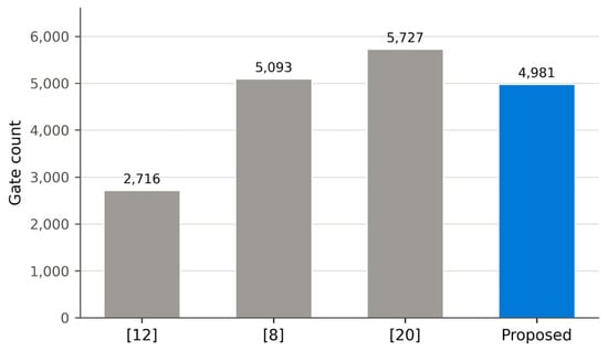
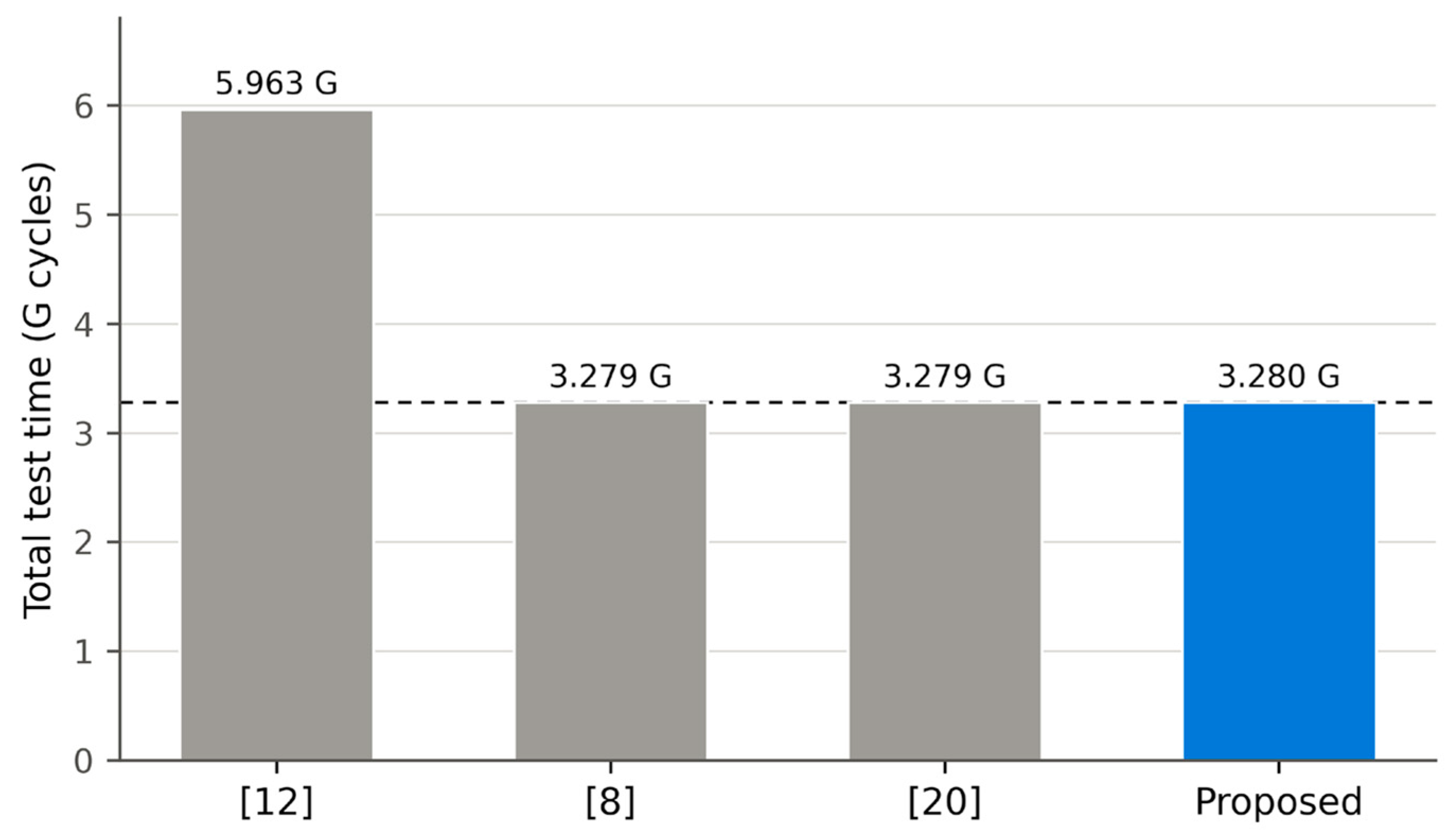
The proposed architecture was implemented in RTL and synthesized with Synopsys Design Compiler using a 14-nm educational standard-cell library, and the fault-data handling paths of the conventional DA transfer [12], the CAM-based fault collection [8], and the signature-based compaction [20] were synthesized under the same conditions. All schemes assume the memory organization of Table 1; the CAM-based scheme [8] has two spare rows and two spare columns with CAM reuse, and the signature-based scheme [20] uses its 64-bit signature. Figure 7 compares the NAND2-equivalent gate counts.
Figure 7.
Hardware overhead comparison.
The conventional DA transfer [12] forms the baseline that every DA-based scheme contains, namely the test register, the comparator, and the result register. The proposed architecture adds the transfer control, the Previous Result Register with its comparison logic, and the fault bit counter, priority encoder, decoder, and index register, all of which are fixed-size circuits determined by the data width alone, so the hardware does not grow with the memory capacity or the number of faults. The hardware of the CAM-based scheme [8] is dominated by the CAM entries and the analysis logic, whose size is determined by the number of spares and the address width and therefore grows with the repair resources and the memory capacity. The hardware of the signature-based scheme [20] is proportional to the data width and the signature length, and the 64-bit signature used in this comparison is the minimum required for the 512-Mbit channel of Table 1. As Figure 7 shows, the proposed architecture requires less hardware than either on-chip scheme while delivering every faulty response to the ATE, and its 83% increase over the conventional DA transfer [12] is a fixed cost that does not scale with the stack capacity.
The dynamic power of the proposed logic was estimated to be 1.2 mW. The logic operates only in the DA test mode, and in functional mode the test clock is stopped and the registers are held in reset, so that only leakage remains. The dominant contributors are the test register, the result register, and the comparator, which the conventional DA transfer [12] also contains. The added logic toggles only on the rare faulty responses, and the suppression of fault-free responses reduces the switching activity of the DA response path in proportion to the response-data reduction in Section 4.2.
The proposed logic resides in the DA test clock domain and is not inserted into the functional I/O path, so the functional timing of the HBM data path is unaffected. Within the test domain, the longest combinational paths are the fault bit counter and the 128-to-7 priority encoder. The synthesized logic met all timing constraints at the 1 GHz clock of Table 1, and because the DA test of HBM operates at a frequency well below this value, the proposed logic imposes no limitation on the DA test clock.
4.4. Test Time Comparison
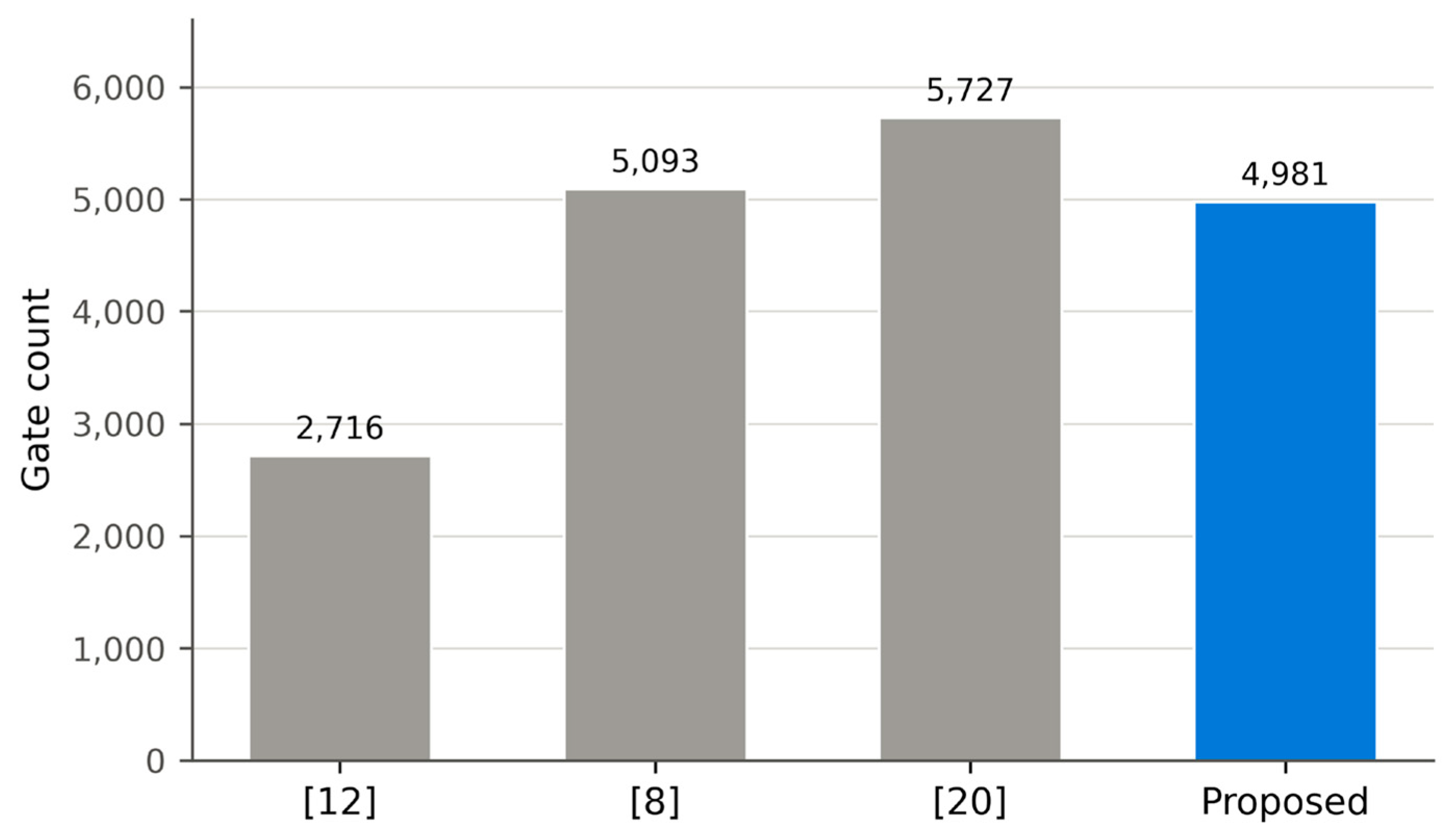
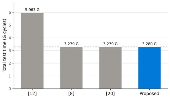
Test time was compared in terms of the total test-cycle count of the same March C− test on the memory organization of Table 1 under the Random Fault model with a fault rate of 1%. The count consists of the memory-operation cycles and the response-handling cycles. The memory-operation cycles include the command and address transfers, the read and write operations, and the timing constraints, and they are common to every scheme, whereas the response-handling cycles are those that each scheme adds. The BIST engines of the on-chip schemes [8,20] were assumed to issue the same command sequence at the same rate as the DA-based test. Figure 8 shows the results. The dashed line marks the memory-operation cycles, which form the lower bound for every scheme.
Figure 8.
Test time comparison.
The conventional DA transfer [12] transfers every 128-bit response serially through the 1-bit DA path after the read latency, without overlapping it with the subsequent read, so each response occupies the path for 128 cycles. The response-handling cycles are therefore comparable to the memory-operation cycles themselves, and the total in Figure 8 is nearly twice the lower bound. The CAM-based fault collection [8] evaluates the responses on-chip, collects the fault addresses concurrently with the test, and completes its repair analysis during the test without additional cycles, so its count equals the memory-operation cycles. The signature-based compaction [20] compacts responses at system speed and downloads the collector registers only once per March element, so the added cycles are negligible compared with the memory-operation cycles, and its count also coincides with the lower bound. The proposed architecture transfers only faulty responses, starts each transfer within the read-latency interval of the subsequent read, and shortens most responses with failing-bit indexing, so the cycles added by the faulty responses are three orders of magnitude fewer than those of the conventional transfer, and the total is indistinguishable from the lower bound at the scale of Figure 8.
Two observations follow from Figure 8. First, the proposed architecture reduces the test time by nearly half compared with the conventional DA transfer and nearly reaches the lower bound set by the on-chip schemes. The response transfer that dominated DA-based testing is thus almost entirely removed even though the response path remains 1 bit wide. Second, the on-chip schemes reach the lower bound by not transferring fault information during the test, and the same property bounds their diagnostic capability, as shown in Section 4.5. The proposed architecture obtains nearly the same test time while every faulty response and its failing-bit positions reach the ATE during the test.
4.5. Diagnostic Coverage Comparison
Diagnostic coverage DC is defined in Equation (8) as the fraction of the faulty cells in a memory whose locations are recovered at the ATE from one execution of the test, where NM is the number of faulty cells in the memory and NL is the number of faulty cells whose locations are recovered.
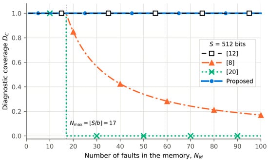
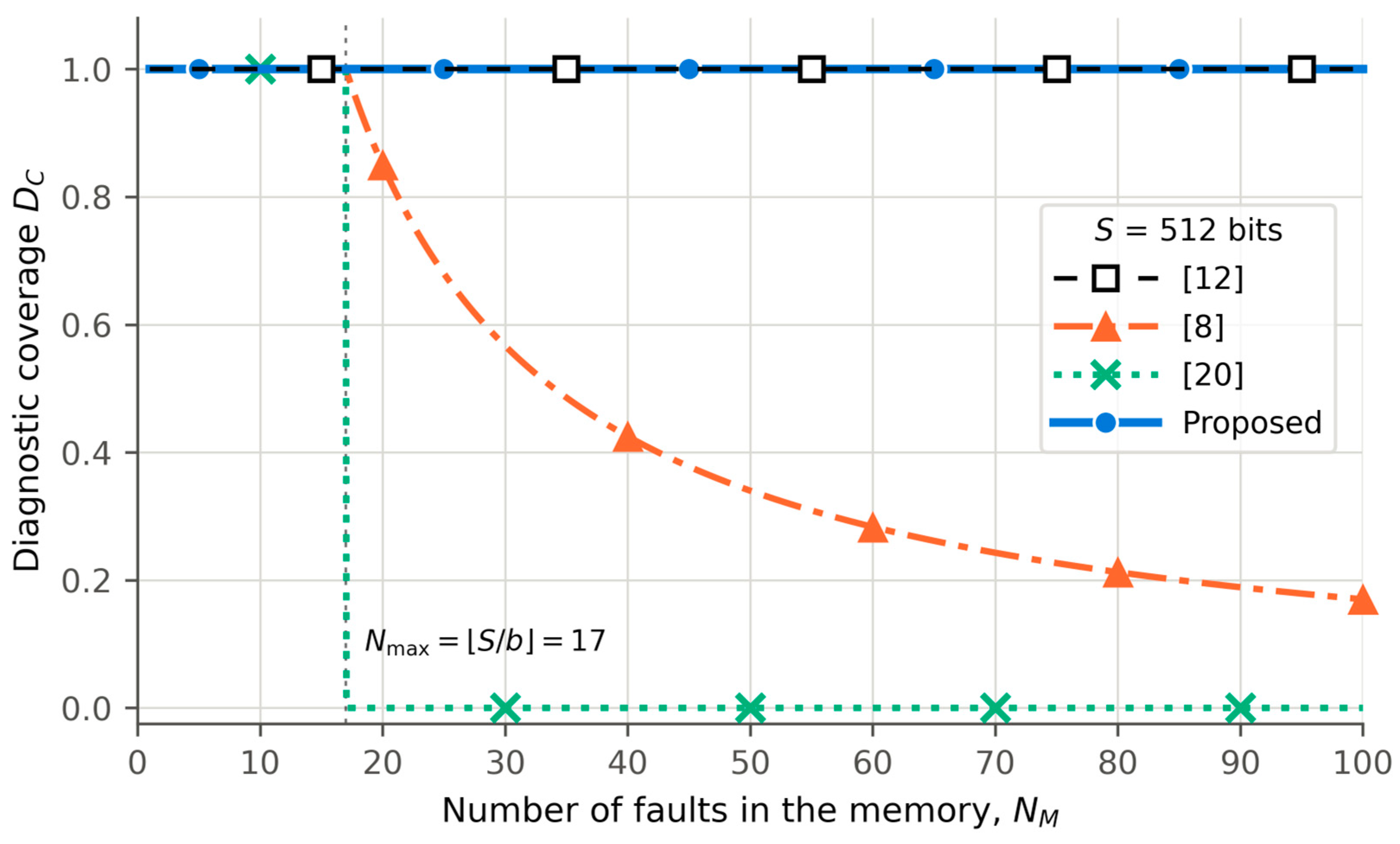
Locating one faulty cell requires its address and the position of the failing bit in the data word. For the memory organization of Table 1, the 4,194,304 addresses are encoded in 22 bits and the position among the 128 data bits in 7 bits, so one location requires b = 29 bits. Because b is the minimum number of bits per location, a scheme that keeps the fault data on-chip in S bits of storage can locate at most Nmax faulty cells, as given by Equation (9), regardless of the storage format. Hence DC = 1 for NM ≤ Nmax, and DC decreases beyond Nmax in a way that depends on how the scheme loses information.
The conventional DA transfer [12] and the proposed architecture transfer every faulty response to the ATE during the test and keep no fault data on-chip, so Equation (9) imposes no bound and DC = 1 for any number of faulty cells. The CAM-based fault collection [8] keeps the first Nmax fault addresses and discards the rest, so its coverage follows Equation (10).
The signature-based compaction [20] compacts the entire error sequence into one value, so the fault set can be identified only while the number of fault locations lies within the resolution of the signature, which is bounded for an S-bit signature in the same manner as Equation (9). Beyond that bound, an aliased signature identifies no individual location, so the coverage follows Equation (11).
DC = 1 for NM ≤ Nmax and DC = 0 for NM > Nmax
Figure 9 compares the diagnostic coverage of the four schemes against the number of faults in the memory, with a common storage of S = 512 bits for the on-chip schemes, which corresponds to Nmax = 17. The coverage of the CAM-based scheme [8] decreases gradually beyond Nmax because the first Nmax faulty cells remain located and the coverage follows Nmax/NM, whereas the coverage of the signature-based scheme [20] drops to zero as soon as NM exceeds Nmax because the signature is decoded either entirely or not at all. The conventional DA transfer and the proposed architecture keep the coverage at 1 over the whole range. A larger or smaller storage shifts Nmax along the horizontal axis of Figure 9 but leaves the shape of the curves unchanged, because any finite S bounds the number of faulty cells that can be located. The on-chip schemes obtain their low test time by retaining a bounded summary of the faults, so a memory whose fault population exceeds that bound can no longer be fully diagnosed from a single test. The proposed architecture, in contrast, retains the full diagnostic coverage of the conventional DA transfer, including the failing-bit positions that neither on-chip scheme delivers, at nearly the test time of the on-chip schemes.
Figure 9.
Diagnostic coverage comparison.
4.6. Overall Comparison
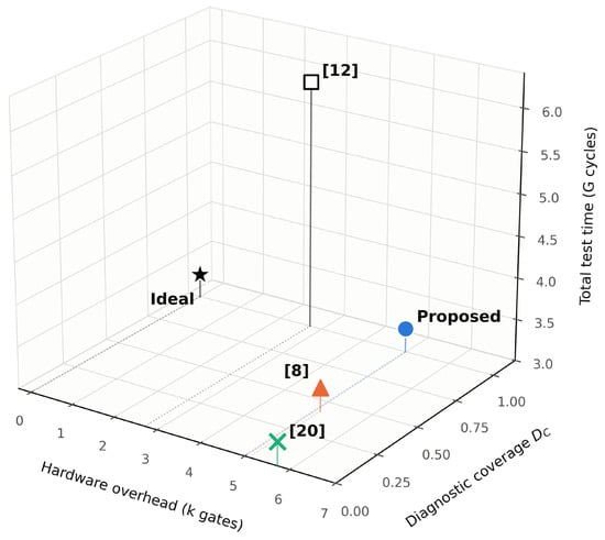
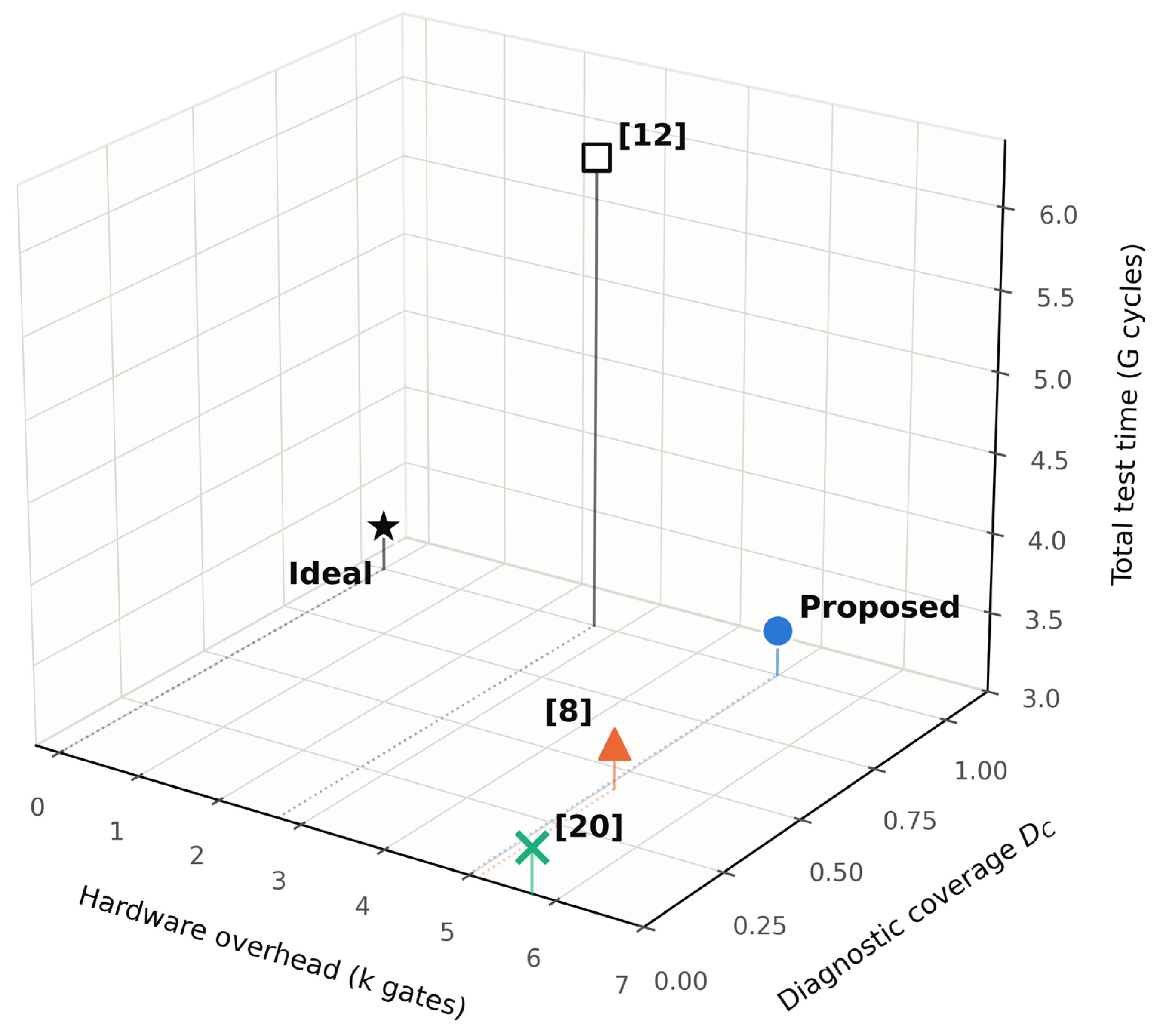
Figure 10 combines the three criteria of Section 4.3, Section 4.4 and Section 4.5 in one chart: the hardware overhead of the fault-data handling path, the total test time under the 1% Random Fault model, and the diagnostic coverage for a fault population that exceeds the retention bound Nmax of the on-chip schemes. An ideal scheme, which would add no hardware, add no response-handling cycles, and lose no fault information, is marked by a star for reference.
Figure 10.
Overall comparison of the proposed architecture and the existing schemes.
The conventional DA transfer [12] has the smallest hardware and full coverage but by far the longest test time, because every response crosses the DA path. The on-chip schemes [8,20] reach the ideal test time at the cost of the largest hardware, and their coverage falls beyond their retention bound. The proposed architecture lies closest to the ideal point. It combines the test time of the on-chip schemes with the coverage of the DA transfer and departs from the ideal point only in the added hardware, which is a fixed cost independent of the memory capacity and the number of faults.
5. Conclusions
In DA-based HBM testing, every read response is transferred through the bandwidth-limited DA response path regardless of whether it contains a fault. Because most responses are fault-free, this fixed-timing transfer incurs substantial overhead and additional test time. To alleviate this bottleneck, this paper proposed a fault-data transfer architecture that controls whether, when, and in which format each response is transferred according to the internal comparison result, while preserving the conventional DA-port interface and the command and address sequence of the March algorithm. Selective staggered read suppresses the external transfer of fault-free responses and overlaps the transfer of a faulty response with the read-latency interval of the subsequent read operation. Duplicate fault suppression replaces identical fault responses at consecutively accessed addresses with a short Duplicate Code, and failing-bit indexing transmits only the positions of the failing bits as 7-bit index codes.
Cycle-accurate simulation of an HBM2 test model showed that, for the Random, Column-Correlated, and Row-Correlated Fault models at fault rates of 0.01–5%, the proposed method reduces the DA response-data volume by 99.32–99.99% and the test time by 44.86–45.01% compared with the conventional method, and the test time reduction is nearly independent of the fault rate. Synthesis showed that the added logic is smaller than that of the CAM-based fault collection and signature-based compaction schemes and independent of the memory capacity and the number of faults. The proposed architecture attains nearly the same test time as the on-chip schemes while delivering every faulty response and its failing-bit positions to the ATE, so that its diagnostic coverage remains complete for any number of faults. By transferring only the fault information that the ATE needs, the proposed method shortens the test time and reduces the response data that the ATE must receive and process, thereby lowering the cost of HBM testing.
The evaluation in this work targeted a single HBM2 channel in Legacy Mode with a 1-bit DA response path and used synthetic fault models, which leaves two directions for future work. First, the single-channel model reflects ATE-based multi-site testing, in which few tester channels are assigned to each stack and the channels of a stack are tested in turn through the same DA resources. Testing the channels concurrently would shorten the test time of a stack at the cost of tester channels and sites. Because the proposed logic is instantiated per channel without shared state and the DA path carries only faulty responses, several channels are expected to share one response signal with little contention. This trade-off and the contention on a shared response signal will be quantified for newer HBM generations with a cycle-accurate multi-channel model that includes pseudo channels. Second, the proposed method will be evaluated with fault distributions observed in real HBM devices and combined with redundancy analysis and built-in self-repair flows, so that the fault information reconstructed by the ATE can be used directly for repair.
Author Contributions
Conceptualization, J.K., E.K. and D.S.; methodology, E.K. and D.S.; software, J.K.; validation, J.K., H.L. and H.-B.L.; investigation, J.K., H.L. and H.-B.L.; writing—original draft preparation, J.K.; writing—review and editing, J.K., E.K., H.L., H.-B.L. and D.S.; visualization, J.K. and E.K.; supervision, D.S.; project administration, D.S.; funding acquisition, D.S. All authors have read and agreed to the published version of the manuscript.
Funding
This work was supported by K-CHIPS (Korea Collaborative & High-tech Initiative for Prospective Semiconductor Research) (2410016659, RS-2025-02305546, 25062-15TC) funded by the Ministry of Trade, Industry & Energy (MOTIE, Republic of Korea).
Data Availability Statement
The original contributions presented in this study are included in the article. Further inquiries can be directed to the corresponding author.
Acknowledgments
The EDA tool was supported by the IC Design Education Center (IDEC), Republic of Korea.
Conflicts of Interest
The authors declare no conflicts of interest.
References
- Tran, K. The era of high bandwidth memory. In Proceedings of the 2016 IEEE Hot Chips 28 Symposium (HCS), Cupertino, CA, USA, 21–23 August 2016; pp. 1–22. [Google Scholar] [CrossRef] [Scilit]
- Chae, J.-H. High-bandwidth and energy-efficient memory interfaces for the data-centric era: Recent advances, design challenges, and future prospects. IEEE Open J. Solid-State Circuits Soc. 2024, 4, 252–264. [Google Scholar] [CrossRef] [Scilit]
- Jun, H.; Cho, J.; Lee, K.; Son, H.-Y.; Kim, K.; Jin, H.; Kim, K. HBM (High Bandwidth Memory) DRAM technology and architecture. In Proceedings of the 2017 IEEE International Memory Workshop (IMW), Monterey, CA, USA, 14–17 May 2017; pp. 1–4. [Google Scholar] [CrossRef] [Scilit]
- Chun, K.C.; Kim, Y.K.; Ryu, Y.; Park, J.; Oh, C.S.; Byun, Y.Y.; Kim, S.Y.; Shin, D.H.; Lee, J.G.; Ho, B.-K.; et al. A 16-GB 640-GB/s HBM2E DRAM with a data-bus window extension technique and a synergetic on-die ECC scheme. IEEE J. Solid-State Circuits 2021, 56, 199–211. [Google Scholar] [CrossRef] [Scilit]
- Jun, H.; Nam, S.K.; Jin, H.H.; Lee, J.-C.; Park, Y.J.; Lee, J. High-bandwidth memory (HBM) test challenges and solutions. IEEE Des. Test. 2017, 34, 16–25. [Google Scholar] [CrossRef] [Scilit]
- Sohn, K.; Yun, W.-J.; Oh, R.; Oh, C.-S.; Seo, S.-Y.; Park, M.-S.; Shin, D.-H.; Jung, W.-C.; Shin, S.-H.; Ryu, J.-M.; et al. A 1.2 V 20 nm 307 GB/s HBM DRAM with at-speed wafer-level IO test scheme and adaptive refresh considering temperature distribution. IEEE J. Solid-State Circuits 2017, 52, 250–260. [Google Scholar] [CrossRef] [Scilit]
- Kim, B.; Shin, S.-H.; Moon, Y.; Jeong, E.; Kang, S. A low-area built-in self-repair using hybrid fault address memory for HBM. IEEE Trans. Very Large Scale Integr. (VLSI) Syst. 2026, 34, 991–1003. [Google Scholar] [CrossRef] [Scilit]
- Yoon, J.; Lee, H.; Moon, Y.; Shin, S.-H.; Kang, S. A built-in self-repair with maximum fault collection and fast analysis method for HBM. IEEE Trans. Comput.-Aided Des. Integr. Circuits Syst. 2025, 44, 2014–2025. [Google Scholar] [CrossRef] [Scilit]
- Du, X.; Mukherjee, N.; Cheng, W.-T.; Reddy, S.M. Full-speed field-programmable memory BIST architecture. In Proceedings of the 2005 IEEE International Test Conference (ITC), Austin, TX, USA, 8–10 November 2005; pp. 1–9. [Google Scholar] [CrossRef] [Scilit]
- Park, Y.; Park, J.; Han, T.; Kang, S. An effective programmable memory BIST for embedded memory. IEICE Trans. Inf. Syst. 2009, E92-D, 2508–2511. [Google Scholar] [CrossRef] [Scilit]
- JESD235D; High Bandwidth Memory DRAM (HBM1, HBM2). JEDEC Solid State Technology Association: Arlington, VA, USA, 2021.
- Lee, D.U.; Kim, K.W.; Kim, K.-W.; Lee, K.S.; Byeon, S.J.; Kim, J.-H.; Cho, J.-H.; Lee, J.; Chun, J.H. A 1.2 V 8 Gb 8-channel 128 GB/s high-bandwidth memory (HBM) stacked DRAM with effective I/O test circuits. IEEE J. Solid-State Circuits 2015, 50, 191–203. [Google Scholar] [CrossRef] [Scilit]
- van de Goor, A.J. Using March tests to test SRAMs. IEEE Des. Test Comput. 1993, 10, 8–14. [Google Scholar] [CrossRef] [Scilit]
- IEEE Std 1500-2022; IEEE Standard Testability Method for Embedded Core-Based Integrated Circuits. IEEE: New York, NY, USA, 2022. [Google Scholar] [CrossRef] [Scilit]
- JESD238A; High Bandwidth Memory DRAM (HBM3). JEDEC Solid State Technology Association: Arlington, VA, USA, 2023.
- Abdennadher, S.; Altmann, M.; Xue, B. Challenges and emerging solutions in testing HBM IO & systems. In Proceedings of the 2018 IEEE 19th Latin-American Test Symposium (LATS), São Paulo, Brazil, 12–14 March 2018; pp. 1–4. [Google Scholar] [CrossRef] [Scilit]
- Han, D.; Lee, H.; Kang, S. Effective spare line allocation built-in redundancy analysis with base common spare for yield improvement of 3D memory. IEEE Access 2021, 9, 76716–76729. [Google Scholar] [CrossRef] [Scilit]
- Cho, K.; Lee, Y.-W.; Seo, S.; Kang, S. An efficient BIRA utilizing characteristics of spare pivot faults. IEEE Trans. Comput.-Aided Des. Integr. Circuits Syst. 2019, 38, 551–561. [Google Scholar] [CrossRef] [Scilit]
- Lee, H.; Han, D.; Lee, S.; Kang, S. Dynamic built-in redundancy analysis for memory repair. IEEE Trans. Very Large Scale Integr. (VLSI) Syst. 2019, 27, 2365–2374. [Google Scholar] [CrossRef] [Scilit]
- Mukherjee, N.; Pogiel, A.; Rajski, J.; Tyszer, J. High volume diagnosis in memory BIST based on compressed failure data. IEEE Trans. Comput.-Aided Des. Integr. Circuits Syst. 2010, 29, 441–453. [Google Scholar] [CrossRef] [Scilit]
- Mukherjee, N.; Pogiel, A.; Rajski, J.; Tyszer, J. High throughput diagnosis via compression of failure data in embedded memory BIST. In Proceedings of the 2008 IEEE International Test Conference (ITC), Santa Clara, CA, USA, 28–30 October 2008; pp. 1–10. [Google Scholar] [CrossRef] [Scilit]
- Hou, C.-S.; Li, J.-F.; Fu, T.-J. A BIST scheme with the ability of diagnostic data compression for RAMs. IEEE Trans. Comput.-Aided Des. Integr. Circuits Syst. 2014, 33, 2020–2024. [Google Scholar] [CrossRef] [Scilit]
- Grzelak, B.; Keim, M.; Pogiel, A.; Rajski, J.; Tyszer, J. Convolutional compaction-based MRAM fault diagnosis. In Proceedings of the 2021 IEEE European Test Symposium (ETS), Bruges, Belgium, 24–28 May 2021; pp. 1–6. [Google Scholar] [CrossRef] [Scilit]
- Bernardi, P.; Grosso, M.; Sonza Reorda, M.; Zhang, Y. A programmable BIST for DRAM testing and diagnosis. In Proceedings of the 2010 IEEE International Test Conference (ITC), Austin, TX, USA, 2–4 November 2010; pp. 1–10. [Google Scholar] [CrossRef] [Scilit]
- Lee, Y.; Lee, Y.W.; Seo, S.; Kang, S. Reduced-pin-count BOST for test-cost reduction. IEEE Trans. Comput.-Aided Des. Integr. Circuits Syst. 2022, 41, 750–761. [Google Scholar] [CrossRef] [Scilit]
- Lee, S.; Lee, H.; Lee, J.; Kang, S. A new pipelined output data reducer of BOST for improved parallelism. IEEE Trans. Comput.-Aided Des. Integr. Circuits Syst. 2025, 44, 765–776. [Google Scholar] [CrossRef] [Scilit]
- Lee, H.; Lee, S.; Kang, S. A new fail address memory architecture for cost-effective ATE. IEEE Trans. Comput.-Aided Des. Integr. Circuits Syst. 2024, 43, 1260–1273. [Google Scholar] [CrossRef] [Scilit]
- Lee, H.; Lee, S.; Kang, S. RA-aware fail data collection architecture for cost reduction. IEEE Trans. Very Large Scale Integr. (VLSI) Syst. 2024, 32, 1136–1149. [Google Scholar] [CrossRef] [Scilit]
- Wu, R.; Zhou, S.; Lu, J.; Shen, Z.; Xu, Z.; Shu, J.; Yang, K.; Lin, F.; Zhang, Y. Removing obstacles before breaking through the memory wall: A close look at HBM errors in the field. In Proceedings of the 2024 USENIX Annual Technical Conference (USENIX ATC ’24), Santa Clara, CA, USA, 10–12 July 2024; pp. 851–867. [Google Scholar]
- Olgun, A.; Osseiran, M.; Yağlıkçı, A.G.; Tuğrul, Y.C.; Luo, H.; Rhyner, S.; Salami, B.; Gómez-Luna, J.; Mutlu, O. Read disturbance in high bandwidth memory: A detailed experimental study on HBM2 DRAM chips. In Proceedings of the 2024 54th Annual IEEE/IFIP International Conference on Dependable Systems and Networks (DSN), Brisbane, Australia, 24–27 June 2024; pp. 75–89. [Google Scholar] [CrossRef] [Scilit]

Disclaimer/Publisher’s Note: The statements, opinions and data contained in all publications are solely those of the individual author(s) and contributor(s) and not of MDPI and/or the editor(s). MDPI and/or the editor(s) disclaim responsibility for any injury to people or property resulting from any ideas, methods, instructions or products referred to in the content. |
© 2026 by the authors. Licensee MDPI, Basel, Switzerland. This article is an open access article distributed under the terms and conditions of the Creative Commons Attribution (CC BY) license.