


Abstract
Thin-film capacitors and supercapacitors are gaining increasing attention due to the rapid development of modern electronics, flexible devices, microsystems and wearable technologies. Their small size, low weight and compatibility with integrated electronic systems make them promising components for next-generation applications and energy-storage systems. In recent years, significant progress has been achieved in the development of thin-film structures with improved capacitance, higher energy density, lower leakage current and better thermal and electrical stability. Advances in thin-film engineering have also enabled the use of high-k dielectric materials, ultrathin insulating layers, oxide-based electrodes and advanced carbon materials to enhance device performance. This review presents recent progress in thin-film capacitor and supercapacitor technologies, focusing on device architectures, dielectric and electrode thin films and reliability-related challenges. Different configurations, including metal–insulator–metal (MIM), metal–oxide–semiconductor (MOS), interdigital, flexible and three-dimensional structures, are discussed. Special attention is given to oxide thin films, nanostructured electrodes, interface quality, defect-related phenomena and scaling effects influencing electrical performance. Current market trends and commercial perspectives are also discussed in the context of emerging electronic applications. Finally, key technological challenges and future development directions for thin-film capacitors and supercapacitors are highlighted.
1. Introduction
The rapid development of modern electronics has significantly increased the demand for high-performance passive components. This trend is driven by the continuous miniaturization of electronic devices and the growing complexity of integrated systems. Modern applications, including the Internet of Things (IoT), wearable electronics, flexible devices, wireless communication systems and advanced microsystems, require components showing smaller dimensions, lower weight and improved electrical performance. At the same time, these components must provide high reliability, low power consumption and compatibility with modern microfabrication technologies [1,2,3].
Capacitors are among the most fundamental passive components in electronic circuits. They are used for energy storage, signal filtering, voltage stabilization, impedance matching, timing circuits, sensing and power management. Their performance directly influences the efficiency and stability of electronic systems [4]. Conventional discrete capacitors have been continuously improved over the past decades. However, their further miniaturization has become increasingly challenging due to physical and technological limitations. This has resulted in a rapid development of thin-film capacitor technologies [5].
Thin-film capacitors are fabricated by depositing functional layers directly onto rigid or flexible substrates. Their compact dimensions and low weight make them attractive for highly integrated electronic systems. Additionally, thin-film technologies enable precise control of film thickness, composition and interface quality. These advantages allow the fabrication of devices with high capacitance density, reduced leakage current and improved dielectric strength. Thin-film capacitors are now widely investigated for applications in integrated circuits, microelectromechanical systems (MEMS), radio-frequency (RF) electronics, sensors, medical devices and flexible electronic platforms [6,7].
In parallel, thin-film supercapacitors have attracted considerable attention as promising energy storage devices. Unlike conventional dielectric capacitors, they store energy through electrochemical mechanisms. This enables significantly higher energy density while maintaining high power density and excellent cycling stability. Their rapid charge–discharge capability makes them particularly attractive for autonomous sensors, wearable electronics, microsystems, and hybrid energy storage platforms. The increasing integration of energy harvesting technologies has further stimulated research on compact thin-film supercapacitors that can operate directly on electronic chips [8,9,10,11].
The performance of thin-film capacitors and supercapacitors depends on several interconnected factors. The dielectric material determines the capacitance, dielectric losses, breakdown strength, and leakage current. Electrode materials influence electrical conductivity, interface stability, and device durability. At the same time, thin-film thickness, crystallinity, surface morphology, interface quality, and defect concentration strongly affect electrical behavior. Consequently, continuous improvements in materials and fabrication technologies remain essential for achieving higher device performance [5,12].
Recent advances in dielectric and electrode materials have significantly improved the performance of thin-film capacitors. However, continued device miniaturization introduces challenges related to leakage current, dielectric breakdown, interface quality, and long-term reliability [6]. Alongside material development, thin-film capacitor architectures have evolved from conventional MIM and MOS structures toward interdigital, flexible, and three-dimensional configurations, offering new opportunities for device miniaturization, integration, and performance optimization [13].
Although numerous reviews have addressed individual aspects of thin-film capacitors and supercapacitors, an integrated perspective combining device architectures, functional thin-film materials, electrical performance, reliability, and emerging applications remains limited. This review therefore provides a comprehensive overview of recent developments in thin-film capacitors and supercapacitors, covering major device architectures, dielectric and electrode materials, key performance and reliability factors, and emerging applications. Current technological challenges, market perspectives, and future research directions are also discussed.
Numerous review articles have addressed different aspects of capacitor and supercapacitor technologies. However, many of these publications focus on specific research topics, particular material groups, or selected device architectures. For example, recent reviews have examined Si-doped CsSrI3 perovskites as potential dielectric materials for MIM capacitors [14], BiFeO3-based dielectric capacitors for energy storage applications [15], or polymer-based capacitors [16]. Other studies have provided broader discussions of capacitor technologies or focused on micro-supercapacitors, flexible devices, and three-dimensional architectures. Although these publications provide valuable insights into individual materials and technologies, the present review adopts a broader perspective, covering different thin-film capacitor and supercapacitor structures. Particular attention is given to functional thin-film materials, fabrication methods, electrical and electrochemical performance, reliability, technological integration, and practical applications. To illustrate the scope and added value of the present work, Table 1 compares the main topics covered in selected previously published reviews.
Table 1.
Comparison of the main topics covered in selected review articles and the present work.
As shown in Table 1, previous reviews have provided valuable discussions of different capacitor and supercapacitor technologies, often emphasizing specific device types, material groups, or fabrication methods. The present review brings together dielectric thin-film capacitors and thin-film-based supercapacitors, including conventional MIM and MOS structures, micro-supercapacitors, flexible devices, and three-dimensional architectures. It discusses how functional materials, fabrication technologies, and device architectures influence electrical and electrochemical performance. In addition, reliability, technological integration, practical applications, and market perspectives are considered. This combined approach provides a broader understanding of current developments and challenges in thin-film capacitor and supercapacitor technologies.
The literature for this review was collected using Google Scholar, ScienceDirect, Web of Science and Scopus. The search focused mainly on studies published between 2015 and 2026, while selected earlier publications were included to provide background information and explain fundamental operating principles. The main search terms included “thin-film capacitors”, “thin-film supercapacitors”, “MIM capacitors”, “MOS capacitors”, “high-k dielectrics”, “micro-supercapacitors”, “functional thin films”, “3D capacitors” and “flexible supercapacitors”. Publications were selected based on their relevance to device architectures, functional materials, fabrication methods, electrical and electrochemical performance, and reliability. Particular attention was given to studies reporting experimental results and quantitative performance parameters. The structures presented as representative examples were selected to illustrate different material systems, device architectures and technological approaches, rather than to identify the best-performing devices. Information on market trends, commercial developments and future market perspectives was additionally obtained from relevant industry reports and market analyses.
2. Thin-Film Capacitor and Supercapacitor Architectures
Capacitors and supercapacitors are both charge-storage devices described by capacitance, but they differ fundamentally in their mechanisms of energy storage. In a conventional dielectric capacitor, two conductive electrodes are separated by an electrically insulating dielectric layer. When a voltage is applied, equal and opposite charges accumulate on the electrodes, while the dielectric becomes polarized. The amount of stored charge and the resulting capacitance depend on the dielectric properties, electrode geometry, and separation between the electrodes. Supercapacitors operate according to a different principle. Instead of storing charge across a conventional solid dielectric layer, charge storage occurs mainly at or near the interface between an electronically conducting electrode and an ionically conducting electrolyte. In electric double-layer capacitors (EDLCs), ions from the electrolyte accumulate at the electrode surface and form an electric double layer. This process is primarily non-Faradaic and does not require charge transfer across the electrode–electrolyte interface. In pseudocapacitors, charge storage additionally involves fast and reversible Faradaic processes occurring at or near the electrode surface. Hybrid supercapacitors can combine different charge-storage mechanisms within a single device. The large accessible electrode–electrolyte interfacial area is one of the main reasons why supercapacitors can achieve much higher capacitance than conventional dielectric capacitors [23,24,25].
These different charge-storage mechanisms result in different characteristic performance parameters and design requirements. Conventional thin-film capacitors are commonly evaluated in terms of capacitance or capacitance density, dielectric loss, leakage current, breakdown strength, quality factor, and frequency response. Supercapacitors are more commonly characterized by gravimetric, areal, or volumetric capacitance, energy density, power density, equivalent series resistance (ESR), rate capability, and cycling stability. Direct comparison of capacitance values between these two device classes can therefore be misleading unless the charge-storage mechanism, normalization method, and device geometry are clearly considered [26,27].
The main differences between conventional dielectric capacitors and supercapacitors are summarized in Table 2. The comparison is intended to provide a common basis for the discussion of thin-film architectures presented in the following sections.
Table 2.
Fundamental differences between conventional dielectric capacitors and supercapacitors.
Despite these fundamental differences, capacitors and supercapacitors share several important architectural concepts. In both cases, device geometry determines how efficiently the available area or volume is used for charge storage. Planar structures provide straightforward integration with thin-film processing, while interdigital geometries enable lateral device configurations. Flexible architectures allow integration with mechanically compliant electronics, and three-dimensional structures increase the effective active area without a proportional increase in device footprint. However, the physical role of this geometrical enhancement differs between the two device classes. In dielectric capacitors, an increased effective area directly increases the electrode area participating in electrostatic charge storage. In supercapacitors, geometrical enhancement is beneficial when it increases the electrochemically accessible electrode–electrolyte interface and maintains efficient ion and electron transport.
This distinction is particularly important for the architectures discussed in the following sections. MIM and MOS structures represent established thin-film capacitor configurations based primarily on dielectric charge separation. Interdigital geometries can be used both for conventional capacitive structures and for planar micro-supercapacitors, although their charge-storage mechanisms remain different. Similarly, flexible and three-dimensional designs can be applied to both device classes to improve mechanical integration or increase the effective charge-storage area. The following sections therefore focus on device architecture, while the properties of the functional dielectric and electrode materials and their influence on device performance are discussed separately in Section 3.
2.1. Metal–Insulator–Metal (MIM) Capacitors
Metal–insulator–metal (MIM) capacitors are among the most common thin-film capacitor structures. A basic MIM capacitor consists of two conductive metal electrodes separated by a thin dielectric layer. The bottom electrode is deposited on a substrate, followed by the dielectric film and the top electrode. This forms a compact layered structure in which the dielectric prevents direct electrical contact between the two electrodes [28]. The described structure has been schematically presented below in Figure 1.
Figure 1.
Schematic representation of a MIM capacitor, showing the metal electrodes, dielectric layer, electrode area (A), dielectric thickness (d), accumulated charges, and electric field (E) across the dielectric.
When a voltage is applied between the electrodes, opposite charges accumulate on their surfaces. The dielectric prevents direct current flow between the electrodes under normal operating conditions. At the same time, the applied electric field causes polarization of the dielectric wherein the electrical energy is stored in the electric field formed across the dielectric layer. This charge-storage mechanism is different from that of supercapacitors [29]. In supercapacitors, energy storage is mainly related to processes at the electrode–electrolyte interface. Depending on the electrode material, these processes include electric double-layer formation, fast Faradaic reactions or a combination of both. Hence, although both device types store electrical energy, MIM capacitors and supercapacitors are based on different physical mechanisms. For an ideal MIM capacitor, the capacitance can be approximated using the parallel-plate capacitor Equation (1):
where C is the capacitance, ε0 is the vacuum permittivity, εr is the relative permittivity of the dielectric, A is the effective electrode area, and d is the dielectric thickness [30].
This equation shows that capacitance can be increased in three main ways: by increasing the dielectric permittivity, increasing the electrode area, or reducing the dielectric thickness. The latter two material and geometrical parameters are especially important for device miniaturization. However, reducing the dielectric thickness also increases the electric field across the dielectric:
where E is the electric field and V is the applied voltage. Therefore, thinner dielectric films can provide higher capacitance, but they can also lead to higher leakage current. At very small thicknesses, tunnelling and defect-assisted charge transport become more important. A high electric field can also lead to dielectric breakdown. The dielectric thickness must therefore provide a balance between high capacitance density, low leakage current, and sufficient dielectric strength [31].
One of the main approaches used to increase capacitance density is the use of high-k dielectric materials. These materials have a relatively high dielectric permittivity. Common examples include Al2O3, HfO2, ZrO2 and TiO2. Their use allows higher capacitance to be obtained without an extreme reduction in the physical thickness of the dielectric [32,33]. A thicker high-k layer can therefore reduce direct tunnelling while maintaining high capacitance. This is one of the main reasons why high-k oxides are widely investigated for thin-film MIM capacitors. However, dielectric permittivity and thickness are not the only parameters that control capacitor performance. The quality of the dielectric film is also important. Real thin films contain structural defects, impurities, and vacancies. In oxide dielectrics, oxygen vacancies can form electronic states within the bandgap. Such states may trap charge carriers or provide additional pathways for charge transport. Depending on the dielectric material and electric field, leakage current may involve several mechanisms, including Schottky emission, Poole–Frenkel emission, trap-assisted tunnelling and direct tunnelling [34,35,36].
The quality of the metal/dielectric interfaces also affects electrical performance. Interface defects and chemical reactions can influence charge trapping and charge injection into the dielectric. The electrode material is therefore important not only because of its electrical conductivity. The electrode should also have good chemical and thermal stability and should form a stable interface with the dielectric. Its work function affects the energy barrier for charge injection. As a result, the electrical properties of a MIM capacitor depend on the complete metal/dielectric/metal stack. Surface morphology is another important factor. Roughness of the bottom electrode can cause local changes in dielectric thickness. A locally thinner dielectric region is exposed to a stronger electric field at the same applied voltage. Such regions may therefore show higher leakage current and can become weak points where dielectric breakdown begins. This effect becomes especially important for dielectric layers with thicknesses in the nanometer range. Smooth interfaces and uniform dielectric films are therefore required for reliable MIM capacitors [37,38].
Thin-film deposition methods play an important role in controlling these properties. Atomic layer deposition (ALD) is widely used for dielectric layers because it provides precise thickness control and high film uniformity. It also enables conformal deposition on complex surfaces. These properties are especially important for nanometer-scale dielectrics and three-dimensional capacitor structures. Physical vapor deposition (PVD), sputtering, thermal evaporation, and electron-beam evaporation can be used for the deposition of metallic electrodes. The selected deposition method affects film morphology, thickness, defect concentration and interface quality. It can therefore have a direct effect on the electrical properties of the final capacitor [39,40,41,42].
A wide range of dielectric materials and dielectric stacks has been investigated for thin-film MIM capacitors. In addition to single high-k oxide layers, multilayer and nanolaminate structures are increasingly used to control the balance between capacitance density, leakage current and dielectric strength. The electrical properties also depend on dielectric thickness, electrode materials and deposition conditions. Representative MIM capacitor structures reported in the literature are summarized in Table 3.
Table 3.
Representative thin-film MIM capacitor structures reported in the literature.
As shown in Table 3, high capacitance density can be obtained using both single high-k dielectric layers and engineered multilayer structures. However, increasing the dielectric constant alone does not guarantee good device performance. Leakage current, dielectric strength, voltage stability and interface quality must also be considered. Multilayer structures are particularly useful because materials with different properties can be combined within one dielectric stack. A high-k layer can provide high capacitance, while additional insulating layers can limit charge transport and improve electrical stability. The examples also show that thin-film MIM technology can be extended from conventional rigid substrates to flexible electronic platforms.
2.2. Metal–Oxide–Semiconductor (MOS) Capacitors
Metal–oxide–semiconductor (MOS) capacitors are another important group of thin-film capacitor structures. A basic MOS capacitor consists of a conductive gate electrode, a thin insulating oxide layer, and a semiconductor, as schematically shown in Figure 2.
Figure 2.
Schematic representation of a MOS capacitor and its main operating regimes for a p-type semiconductor: (a) basic MOS structure, (b) accumulation of majority carriers, (c) formation of the depletion region and (d) inversion with minority-carrier accumulation at the semiconductor surface.
In contrast to MIM capacitors, one of the metal electrodes is therefore replaced by a semiconductor. Silicon is the classical semiconductor used in MOS structures, while SiO2 has traditionally been used as the insulating layer. However, high-k oxides such as Al2O3, HfO2, and ZrO2 are increasingly investigated as alternative dielectric materials [49].
The replacement of one metal electrode by a semiconductor strongly changes the electrical behavior of the capacitor. In a metal, the concentration of free charge carriers is high and is only weakly affected by the applied voltage. In a semiconductor, both the concentration and spatial distribution of electrons and holes near the oxide/semiconductor interface can change with the gate voltage. Therefore, the capacitance of a MOS structure is strongly related to the electrical response of the semiconductor [50].
The oxide layer itself can be described using the parallel-plate capacitor relation (3):
where Cox is the oxide capacitance, ε0 is the vacuum permittivity, εox is the relative permittivity of the oxide, A is the gate area, and tox is the oxide thickness.
A thinner oxide or a material with higher dielectric permittivity therefore provides a higher oxide capacitance. However, unlike in an ideal MIM capacitor, the total capacitance of a MOS structure also depends on the response of the semiconductor. This behavior can be explained using a p-type semiconductor as an example. Depending on the gate voltage, the MOS capacitor can operate in three main regimes: accumulation, depletion and inversion. These regimes result from changes in the distribution of charge carriers near the oxide/semiconductor interface and are accompanied by bending of the semiconductor energy bands. When a negative voltage is applied to the gate, holes, which are the majority carriers in a p-type semiconductor, are attracted toward the oxide/semiconductor interface. Their concentration near the surface increases and the device enters the accumulation regime. In this state, the semiconductor surface contains a high concentration of mobile charge carriers and the measured capacitance approaches the oxide capacitance Cox. When the gate voltage becomes more positive, holes are repelled from the semiconductor surface. A region depleted of mobile majority carriers is formed below the oxide. This depletion region mainly contains fixed ionized acceptor atoms and behaves as an additional capacitive region. The oxide capacitance and depletion capacitance can therefore be approximately treated as two capacitors connected in series based on the following Equation (4):
where Cdep is the capacitance associated with the depletion region. As the depletion width increases, Cdep decreases, which causes a decrease in the total measured capacitance [51,52].
At a sufficiently positive gate voltage, the concentration of minority carriers near the semiconductor surface increases. For a p-type semiconductor, these minority carriers are electrons. When their concentration at the surface becomes sufficiently high, an inversion layer is formed and the surface behaves locally as an n-type region. The transition between accumulation, depletion, and inversion is directly reflected in the capacitance–voltage (C–V) characteristic of the MOS capacitor. The shape of the C–V curve also depends on the measurement frequency. At low frequencies, minority carriers can respond to the alternating measurement signal and contribute to the measured capacitance in inversion. At sufficiently high frequencies, their response may be too slow, and the capacitance remains close to its minimum value in strong inversion. Consequently, both the applied gate voltage and measurement frequency must be considered when interpreting MOS capacitance measurements [53,54,55].
The C–V characteristic provides considerably more information than the capacitance value alone. It can be used to determine parameters such as the oxide capacitance, flat-band voltage, semiconductor doping concentration, and properties of the oxide/semiconductor interface. Deviations from the ideal C–V curve can also indicate the presence of electrically active defects. For example, interface traps can cause stretching and frequency dispersion of the C–V characteristic, while fixed oxide charges can shift the curve along the voltage axis. Charge trapping in the dielectric or near the interface can also produce hysteresis between forward and reverse voltage sweeps. Such effects have been observed experimentally in MOS structures based on Si as well as compound semiconductors such as GaN and GaSb [56].
The oxide/semiconductor interface is therefore one of the most important regions of a MOS capacitor. Dangling bonds, native oxides, impurities, structural defects, and chemical reactions at the interface can introduce electronic states within the semiconductor bandgap. These states can trap and release charge carriers and consequently affect capacitance, threshold-related voltages, leakage current, and electrical stability. In Al2O3/GaN MOS capacitors, for example, appropriate surface treatment before dielectric deposition has been shown to reduce the interface-state density to the order of 1011 cm−2 eV−1 and strongly reduce C–V hysteresis and frequency dispersion [57].
The choice of dielectric material is also important. Reduction in the SiO2 thickness increases capacitance, but very thin insulating layers can lead to increased tunnelling current. High-k materials provide an alternative approach because they allow a high capacitance to be obtained with a larger physical dielectric thickness. Al2O3 is frequently used in MOS structures because of its relatively high dielectric permittivity, wide bandgap, and good insulating properties. HfO2 and other high-k oxides can provide even higher dielectric permittivity. However, their practical performance depends not only on the dielectric constant but also on band alignment, defect density, thermal stability, and interface quality [58,59].
ALD is particularly important for the fabrication of thin high-k gate dielectrics. It provides precise thickness control and allows uniform and conformal films to be deposited at the nanometer scale. However, the final electrical properties depend strongly on the surface condition before deposition and on the ALD process itself. For example, different oxidants used during ALD of Al2O3 on GaN have been shown to change the interface trap density [60]. Surface cleaning, chemical passivation, plasma treatment, and post-deposition annealing can therefore be used to improve the oxide/semiconductor interface. In Al2O3/GaN MOS structures, surface passivation has produced substantial reductions in interface and border traps, while annealing has also been shown to modify the C–V response of Al2O3/Si structures [61,62].
MOS capacitors are not limited to silicon-based systems. The development of wide-bandgap and two-dimensional semiconductors has increased interest in MOS structures based on materials such as GaN and transition-metal dichalcogenides. In GaN devices, control of the dielectric/GaN interface is particularly important for power electronic applications. MOS capacitors have also been fabricated on MoS2 using ALD-grown HfO2 and Al2O3. In these structures, C–V frequency dispersion provides information about defects at the high-k/MoS2 interface, while the chemically inert MoS2 surface creates additional challenges for uniform dielectric nucleation [63,64,65].
Representative thin-film MOS capacitor structures reported in the literature are summarized in Table 4. The selected examples illustrate the use of different semiconductor/dielectric combinations and show the importance of dielectric deposition, interface engineering, and surface treatment.
Table 4.
Representative thin-film MOS capacitor structures reported in the literature.
As shown in Table 4, the electrical behavior of MOS capacitors depends strongly on both the dielectric material and the semiconductor surface. The interface becomes particularly important when high-k dielectrics are combined with compound or two-dimensional semiconductors. Surface treatment and dielectric deposition conditions can change the density of electrically active traps and consequently affect C–V hysteresis and frequency dispersion. The examples also show why MOS capacitors are useful not only as capacitor structures but also as test devices for evaluating new dielectric/semiconductor interfaces.
MOS capacitors are fundamental structures in semiconductor technology. Their operating principle forms the basis of the gate stack used in metal–oxide–semiconductor field-effect transistors (MOSFETs), while MOS capacitor test structures are widely used to evaluate gate dielectrics, semiconductor surfaces, interface quality, and charge trapping. The development of thin high-k films and improved interface-engineering methods therefore remains important for silicon electronics as well as emerging wide-bandgap and two-dimensional semiconductor devices.
2.3. Interdigital Capacitor Structures
Interdigital capacitor structures are based on two sets of conductive electrodes arranged in an interlocking finger-like pattern on the same plane. In contrast to MIM and MOS capacitors, where the main functional layers are stacked vertically, interdigital structures use an in-plane electrode geometry. The two electrodes are electrically isolated from each other by narrow gaps, while their alternating fingers increase the effective interaction length between the electrodes. A schematic representation of this architecture is shown in Figure 3.
Figure 3.
Schematic representation of interdigital capacitor architectures: (a) planar interdigitated capacitor with two interlocking conductive electrodes and fringing electric fields between adjacent fingers, and (b) interdigitated micro-supercapacitor with active electrode materials and an electrolyte, where charge is stored at the electrode–electrolyte interface. The blue dashed arrows in (a) indicate the electric field lines, while the red and blue arrows in (b) indicate the movement of cations and anions.
In a conventional interdigital capacitor, capacitance originates mainly from the electric field between adjacent electrode fingers. Unlike in a parallel-plate capacitor, the field is not confined between vertically stacked electrodes. Instead, fringing electric fields extend through the surrounding dielectric and the substrate. The capacitance therefore depends on both the electrode geometry and the dielectric properties of the surrounding materials. The main geometrical parameters include finger width and length, spacing between adjacent fingers, number of fingers, and electrode thickness. These parameters determine the effective interaction region and electric-field distribution. In general, increasing the finger length or number of fingers increases capacitance. Electrode spacing is also important because it controls the coupling between neighboring fingers. The geometry must therefore be optimized together with the properties of the substrate and dielectric layers [70,71].
An important feature of the interdigital geometry is the presence of electric fields above and below the electrode plane. Changes in the permittivity of materials located within this field region can modify the measured capacitance. This makes interdigital structures suitable for capacitive sensing. They have been used for humidity, moisture, and chemical sensing, often in combination with functional layers deposited on the electrode surface [72,73].
The same planar geometry is widely used in micro-supercapacitors (MSCs). However, the charge-storage mechanism is different. Adjacent fingers form the positive and negative electrodes and are in contact with an electrolyte. Charge is therefore stored mainly at or near the electrode–electrolyte interface. Depending on the electrode material, this can involve electric-double-layer formation, pseudocapacitive Faradaic processes, or a combination of both mechanisms [74].
The interdigital configuration offers several advantages for MSCs. Both electrodes can be fabricated on the same substrate. This facilitates integration with miniaturized and on-chip electronics. The planar configuration can also avoid the conventional separator used in stacked devices. Moreover, reducing the distance between adjacent fingers can shorten ion-transport pathways and decrease ionic resistance. This can improve the power capability and frequency response of the device [74,75].
Electrode spacing is therefore an important design parameter. However, the smallest gap does not necessarily provide the highest capacitance. Yuan et al. investigated MSCs with interdigital gaps of 200 nm, 500 nm, 1 μm and 2 μm. The gap affected both the electric-field distribution and electrochemical response. The highest capacitance was obtained for an intermediate gap of 500 nm. This result shows that electrode geometry should be optimized rather than simply minimized. Electrode thickness must also be considered. Increasing the thickness can increase the amount of active material and the areal capacitance. However, thicker electrodes may increase ion-transport distances and limit material utilization. The electrode architecture should therefore provide sufficient active material while maintaining efficient ionic and electronic transport [76].
Several methods can be used to fabricate interdigital structures. Photolithography provides precise control of electrode dimensions and is compatible with semiconductor processing. Laser patterning enables direct and mask-free fabrication of microscale structures. Printing techniques provide an alternative route for flexible and large-area devices. The selected method influences the achievable feature size, electrode morphology, thickness and substrate compatibility [77,78,79].
Despite their similar geometry, conventional interdigital capacitors and interdigitated MSCs require different performance parameters. Dielectric capacitors are typically evaluated using capacitance, dielectric loss, quality factor, frequency response, and breakdown behavior. MSCs are commonly characterized using areal or volumetric capacitance, energy and power density, equivalent series resistance, rate capability, and cycling stability. Representative interdigital capacitor and micro-supercapacitor structures are summarized in Table 5.
Table 5.
Representative interdigitated micro-supercapacitors reported in the literature.
As shown in Table 5, the performance of interdigitated MSCs depends on both electrode material and device geometry. High surface area and electrochemical activity increase the amount of stored charge, while short ion-transport pathways and good electrical conductivity support high-rate operation. The planar configuration also allows these properties to be combined within a small device footprint. Importantly, optimization of the finger dimensions, electrode thickness, and inter-electrode spacing must be considered together with the properties of the active material.
One of the main advantages of interdigital architectures is their compatibility with miniaturized and integrated electronics. Planar MSCs can be fabricated directly on rigid or flexible substrates and integrated with sensors, energy harvesters and other microdevices. This makes them attractive for wearable electronics, autonomous sensors, Internet of Things devices and other systems that require compact local energy storage. Recent research is increasingly focused on multifunctional MSCs that combine energy storage with flexibility, stretchability, self-healing, electrochromic behavior or integration with energy-harvesting components [82,83,84].
2.4. Flexible Thin-Film Capacitors
Flexible thin-film capacitors are designed to maintain their electrical or electrochemical performance during mechanical deformation. Unlike conventional devices fabricated on rigid substrates, flexible capacitors are formed on mechanically compliant substrates that allow bending, folding, or other forms of deformation [85,86]. Different capacitor architectures can be adapted to flexible systems, including vertically stacked thin-film capacitors and planar interdigital structures. Flexible supercapacitors can also be fabricated in planar, stacked, fiber-shaped or textile configurations. In all cases, flexibility requires the complete device structure to remain functional during deformation, as schematically illustrated in Figure 4.
Figure 4.
Schematic representation of flexible thin-film energy-storage devices: (a) flexible thin-film capacitor with a multilayer structure on a flexible substrate, illustrating tensile and compressive strain during bending, and (b) flexible supercapacitor with interdigitated electrodes and an electrolyte. The red and blue arrows indicate tensile and compressive strain.
Flexibility does not introduce a separate charge-storage mechanism. Flexible dielectric capacitors still store charge through dielectric polarization. Flexible supercapacitors rely on electrochemical processes at or near the electrode–electrolyte interface. The main difference from rigid devices is therefore mechanical. The substrate, electrodes, functional layers, and interfaces must tolerate deformation while maintaining stable electrical or electrochemical performance [87].
Mechanical strain is one of the main factors affecting flexible thin-film devices. During bending, the outer part of the structure experiences tensile strain, while the inner part is compressed. Between these regions, a neutral mechanical plane exists where the strain approaches zero). The strain within the functional layers depends on the device thickness, bending radius, and position relative to the neutral plane. Thinner structures and larger bending radii generally reduce the generated strain. Placing mechanically sensitive layers close to the neutral plane can further improve their resistance to bending. Mechanical deformation can affect several components simultaneously. Conductive layers may crack, interfaces may delaminate, and defects may develop within functional films. These changes can increase resistance and leakage current or modify capacitance. They can also reduce dielectric strength. In supercapacitors, deformation may additionally affect electrode–electrolyte contact and charge transport. Flexibility should therefore be evaluated through both mechanical deformation and the corresponding change in device performance [88,89].
The substrate strongly influences the mechanical properties and available fabrication conditions. Polymer films are widely used because of their low thickness, low mass, and mechanical compliance. Metal foils, paper, textiles, and other flexible supports can also be employed. However, flexible substrates may limit processing temperature and restrict the available deposition or patterning methods. Good adhesion between individual layers is also required to prevent delamination during repeated deformation [86,89].
Device thickness is another important design parameter. Reducing the total thickness generally improves bendability and decreases bending-induced strain. However, the individual layers must remain continuous and electrically functional. This is particularly important in multilayer devices. Differences in mechanical properties between adjacent layers can produce local stress concentrations at their interfaces. Several fabrication methods can be adapted to flexible devices. Vacuum-based deposition techniques provide good control of thin-film thickness and uniformity. Printing, coating, electrodeposition, and laser patterning provide alternative routes for flexible and large-area structures. Low-temperature processing is particularly important for polymer substrates. For flexible supercapacitors, planar, interdigital, fiber-shaped, and textile architectures can be used. Gel and solid-state electrolytes are also attractive because they facilitate compact device construction and avoid problems associated with liquid-electrolyte leakage [90,91].
Mechanical testing is essential for evaluating flexible capacitors and supercapacitors. Devices are commonly tested at different bending radii, bending angles, or strains. Repeated bending cycles are used to evaluate mechanical durability. These tests should be accompanied by electrical or electrochemical measurements. For dielectric capacitors, capacitance, leakage current, dielectric loss, and resistance can be monitored. For supercapacitors, capacitance retention, equivalent series resistance, charge–discharge behavior, and impedance provide information about electrochemical stability during deformation [92].
Direct comparison between reported flexible devices remains difficult. Bending radius, bending angle, strain, number of cycles, device thickness, and measurement conditions differ between studies. Some devices are characterized during bending, while others are measured only after deformation. Mechanical parameters should therefore be considered together with the corresponding performance retention. Representative flexible capacitor and supercapacitor structures are summarized in Table 6.
Table 6.
Representative flexible thin-film capacitor and supercapacitor architectures and their mechanical stability.
As summarized in Table 6, flexible capacitors and supercapacitors can maintain stable electrical or electrochemical performance under repeated mechanical deformation. However, direct comparison between individual devices remains difficult because flexibility is evaluated using different parameters, including bending radius, bending angle, strain, and number of deformation cycles. Importantly, mechanical deformation should be considered together with the corresponding change in device performance, since the ability to withstand a small bending radius or a large number of bending cycles does not itself demonstrate functional stability. The reported studies therefore highlight the importance of evaluating both mechanical durability and performance retention when assessing flexible energy-storage devices. This combined mechanical and functional stability is particularly important for wearable and conformable electronics, where energy-storage components may be subjected to repeated deformation during normal operation.
2.5. Three-Dimensional Capacitor Architectures
Three-dimensional (3D) capacitor architectures are designed to increase the effective surface area available for charge storage without a proportional increase in the planar footprint of the device. In conventional planar capacitors, the available electrode area is directly limited by the lateral dimensions of the structure. This becomes an important limitation in highly integrated electronic systems, where the available chip area is restricted. Three-dimensional architectures address this problem by extending the active structure in the vertical direction using trenches, pores, pillars, nanowires, or other high-aspect-ratio features. The basic concept of a 3D thin-film capacitor is illustrated in Figure 5. Instead of depositing the electrode–dielectric–electrode stack only on a flat surface, the functional layers are conformally deposited over a structured substrate. The resulting device can therefore provide a considerably larger effective electrode area than a planar capacitor occupying the same projected area [102,103].
Figure 5.
Comparison of planar and three-dimensional energy-storage architectures: (a) planar thin-film capacitor, (b) planar thin-film supercapacitor, (c) 3D thin-film capacitor, and (d) 3D micro-supercapacitor, illustrating the increased effective surface area enabled by three-dimensional structuring. The red and blue arrows indicate the movement of cations and anions.
For a dielectric capacitor, the benefit of increasing the effective surface area follows directly from the basic capacitance relation (5):
where Aeff represents the effective electrode area. In a planar structure, this area is closely related to the device footprint. In a 3D architecture, Aeff can be much larger because the capacitor stack follows the sidewalls and surfaces of the three-dimensional features. Consequently, capacitance per unit planar area can be increased without necessarily reducing the dielectric thickness. This distinction is important because increasing capacitance by decreasing dielectric thickness is accompanied by an increase in electric field at a given voltage and can increase tunnelling, leakage current, and breakdown-related problems. Three-dimensional structuring provides an alternative scaling strategy in which capacitance density is increased mainly through geometrical area enhancement. The final performance nevertheless depends on both the geometrical enhancement and the electrical quality of the deposited capacitor stack. Deep-trench capacitors are an important example of three-dimensional capacitor architectures. High-aspect-ratio trenches are formed in a substrate and coated with the functional capacitor layers. The trench sidewalls and bottom surfaces increase the effective capacitor area without increasing the device footprint. This approach is particularly attractive for integrated capacitors with high capacitance density. The aspect ratio describes the relation between the depth or height of a feature and its lateral dimension. A high aspect ratio can provide a large surface-area enhancement within a small projected area. For example, Si-based 3D MIM capacitors with deep trenches and an aspect ratio of approximately 30:1 have been demonstrated. The trenches were produced by deep reactive ion etching (DRIE). The capacitor stack was subsequently deposited by ALD. Increasing the aspect ratio also makes fabrication more demanding. The dielectric and electrode layers must uniformly cover the top surface, sidewalls, and bottom of the 3D structure. Non-uniform coverage can produce variations in dielectric thickness and local electric-field concentration. It can also increase leakage current and reduce breakdown reliability. Conformal deposition is therefore essential for high-aspect-ratio capacitors. ALD is particularly suitable for this purpose because its surface-controlled growth enables conformal deposition on complex 3D surfaces [104,105].
Three-dimensional architectures are also attractive for MSCs. In planar MSCs, active-material loading is limited by the available footprint. Simply increasing electrode thickness can restrict electrolyte accessibility and increase ion-transport distances. A 3D scaffold provides another strategy. It increases the available electrode surface and active-material loading while maintaining a small projected device area. Different structures can be used for this purpose. Examples include pillars, tubes, pores, nanowires, and hierarchical micro- and nanostructures. The active material is deposited on or incorporated into the 3D scaffold. This increases the electrode–electrolyte interfacial area available for charge storage. Three-dimensional interdigitated structures can further combine planar integration with surface-area enhancement in the vertical direction [106,107,108].
The geometrical benefit of a 3D structure can be described using the area enhancement factor (AEF). This parameter compares the effective surface area of a 3D structure with its projected footprint area. A higher AEF provides more surface within the same footprint. However, geometrical area alone does not determine device performance. The additional surface must remain electrically connected and accessible to the electrolyte. In dielectric capacitors, it must also be uniformly covered by the complete capacitor stack. Ion and electron transport are therefore important in 3D MSCs. Dense structures can provide a high surface area but may restrict electrolyte penetration. Thick active layers can increase material loading but may increase ion-transport distances. The optimum architecture must therefore balance surface area, active-material loading, electrolyte accessibility, and electrical conductivity. Hierarchical structures are particularly attractive because they can combine high surface area with open pathways for ion transport. Three-dimensional architectures can be fabricated using both top-down and bottom-up methods. Lithography, etching, and micromachining can produce trenches, pores, and micropillars. Bottom-up approaches can form nanowires, nanotubes, and other nanostructured scaffolds. More recently, additive manufacturing and laser-based processing have provided additional routes for complex 3D electrodes [106,107,108,109].
Despite their advantages, 3D architectures introduce additional fabrication challenges. These include conformal deposition, defect control, electrical continuity, electrolyte infiltration, and device integration. The highest geometrical surface area therefore does not necessarily provide the best practical performance. The complete architecture must be optimized for both charge storage and transport. Representative 3D capacitor and micro-supercapacitor architectures are summarized in Table 7.
Table 7.
Representative three-dimensional capacitor and micro-supercapacitor architectures reported in the literature.
As summarized in Table 7, the main advantage of three-dimensional architectures is the possibility of increasing the active surface area and charge-storage capability within a limited device footprint. However, the benefit obtained from geometrical enhancement depends on the accessibility and electrical functionality of the additional surface. In dielectric capacitors, this requires uniform and defect-free coverage of complex surfaces by the electrode–dielectric stack, whereas in micro-supercapacitors the 3D electrode must additionally provide efficient electrolyte penetration and ion transport.
Three-dimensional architectures therefore represent an important route toward increasing the capacitance and energy-storage capability of miniaturized devices without increasing their lateral dimensions. Their further development requires simultaneous optimization of geometry, fabrication precision, conformal coating, transport pathways, and device integration. These requirements are particularly important for on-chip capacitors and micro-supercapacitors, where high charge-storage capability must be combined with a small footprint and compatibility with microelectronic fabrication technologies.
2.6. Comparative Assessment of Capacitor and Supercapacitor Architectures
The selection of a capacitor or supercapacitor architecture depends on the intended application, as different structures offer different advantages and limitations. Conventional MIM capacitors provide a relatively simple structure and can be integrated with thin-film deposition technologies. However, their electrical performance depends strongly on dielectric properties, interface quality, leakage current, and capacitance stability under applied voltage [4]. MOS capacitors, in contrast, exhibit capacitance changes associated with the redistribution of charge carriers in the semiconductor, making their electrical behavior strongly dependent on the applied bias. Therefore, these two architectures serve different technological purposes and cannot be directly compared based on capacitance alone.
In micro-supercapacitors, planar interdigital architectures are attractive because they allow short ion transport distances and integration on a common substrate. Three-dimensional electrode structures can further increase the amount of active material and the available electrode surface within a limited device footprint, potentially improving areal energy storage performance [114,115]. However, these benefits depend on the accessibility of active surfaces and efficient ion and electron transport. Increasing electrode thickness or structural complexity does not necessarily improve practical performance, particularly when transport limitations become significant. Moreover, three-dimensional devices may require more complex fabrication, electrolyte incorporation, and packaging processes, which can limit their scalability and integration [106].
Flexible architectures are particularly attractive for wearable and portable electronics, where devices must operate under mechanical deformation. Their practical advantage is therefore related not only to electrochemical performance but also to their ability to maintain stable properties during bending or stretching. This requires suitable electrode materials, flexible substrates, and stable interfaces between the device components. Consequently, the most appropriate architecture should be selected by considering electrical or electrochemical performance together with fabrication requirements, mechanical stability, and compatibility with the intended application [19,21].
3. Dielectric and Electrode Thin Films for Capacitor Applications
The performance of thin-film capacitors and supercapacitors is determined not only by device architecture but also by the properties of the functional materials forming the active layers and interfaces. Dielectric permittivity, electrical conductivity, polarization behavior, defect concentration, surface and interface quality, and electrochemical activity directly influence charge storage and energy-storage performance. The selection and processing of functional thin films are therefore essential for controlling capacitance, energy density, electrical losses, leakage current, breakdown behavior, and long-term stability [13,116].
This section discusses the main groups of functional thin films used in capacitor and supercapacitor technologies and relates their physical and chemical properties to device performance. Particular attention is given to high-k dielectric and ferroelectric thin films, followed by electrode materials used in conventional capacitors and electrochemical energy-storage devices.
3.1. High-k Dielectric Thin Films
Dielectric thin films are key functional components of conventional thin-film capacitors. They electrically separate conductive electrodes and enable energy storage through polarization. For miniaturized devices, the dielectric should provide high capacitance while maintaining low leakage current, low dielectric loss, and sufficient breakdown strength. These requirements have increased interest in materials with high relative dielectric permittivity, commonly referred to as high-k dielectrics [117].
Dielectric permittivity reflects the ability of a material to polarize in response to an applied electric field. Several polarization mechanisms can contribute to the dielectric response. Electronic polarization results from displacement of the electron cloud relative to the atomic nucleus, while ionic polarization involves displacement of ions within the crystal lattice. Dipolar and interfacial polarization may also contribute depending on the material structure. Since these mechanisms operate on different time scales, the dielectric response can vary with frequency. Slower polarization mechanisms become less effective at higher frequencies, which can affect both permittivity and dielectric loss. High permittivity enables increased capacitance without requiring extremely thin dielectric layers. However, k cannot be considered independently of other electrical properties. A suitable dielectric should combine high permittivity with a sufficiently wide bandgap, favorable band alignment with the electrodes, low defect density, low dielectric loss, and high breakdown strength. These requirements often compete with each other. For example, materials with very high permittivity may exhibit a smaller bandgap or lower carrier-injection barriers, which can increase leakage current [118,119].
Defects and microstructure also strongly influence dielectric performance. Impurities, oxygen vacancies, and other structural defects can introduce electronic states within the bandgap and contribute to charge trapping or defect-assisted conduction. Crystallization may modify dielectric permittivity but can also introduce grain boundaries that provide preferential leakage pathways. The concentration and distribution of these defects depend on film composition, deposition conditions, and post-deposition processing. The electrode–dielectric interface is equally important. Interfacial reactions, contamination, roughness, and unintended interlayers can modify carrier-injection barriers and local electric-field distribution. These effects become particularly important for very thin dielectric layers, where defects and thickness non-uniformities can strongly affect leakage and breakdown behavior [120].
Among the most important high-k oxides used in thin-film capacitors are Al2O3, HfO2, ZrO2, TiO2, and Ta2O5. Al2O3 provides good insulating properties and a relatively wide bandgap, although its dielectric permittivity is moderate. HfO2 and ZrO2 offer higher permittivity and are attractive for scaled dielectric structures. TiO2 can provide a particularly high dielectric response, but leakage current may become a limitation. Ta2O5 combines relatively high permittivity with established use in capacitor technologies. Their final properties depend strongly on composition, phase, film thickness, and processing conditions [121,122].
3.2. Ferroelectric Thin Films
Ferroelectric thin films represent an important class of functional dielectric materials because their polarization can be reversibly switched by an external electric field. In contrast to conventional linear dielectrics, ferroelectric materials exhibit spontaneous polarization even in the absence of an applied field. This behavior originates from a non-centrosymmetric crystal structure, in which the centers of positive and negative charge do not coincide. The resulting electric dipole moments form ferroelectric domains, which can reorient under an applied electric field. This makes ferroelectric thin films attractive for capacitors, energy-storage devices, sensors, and integrated electronic systems [123,124].
The electrical response of a ferroelectric material is commonly described by the polarization–electric field (P–E) hysteresis loop. Important parameters include the remanent polarization Pr, saturation or maximum polarization Pmax, and coercive field Ec. For capacitor applications, the recoverable energy density corresponds to the area associated with the discharge branch of the P–E loop:
where Pmax is the maximum polarization reached under the applied electric field. The recoverable energy density is determined from the discharge branch of the P–E loop:
while the energy-storage efficiency can be expressed as:
The difference between the supplied and recoverable energy represents the energy dissipated during polarization switching and is related to the hysteresis-loop area. Consequently, a large Pmax alone does not ensure efficient energy storage. High Wrec generally requires a large difference between Pmax and Pr, together with a relatively narrow hysteresis loop and high dielectric breakdown strength. Materials exhibiting slim P–E loops are therefore particularly attractive for energy-storage applications [125,126].
Classical ferroelectric materials include BaTiO3 (BTO) and Pb(Zr,Ti)O3 (PZT), which exhibit spontaneous polarization associated with their non-centrosymmetric crystal structures. PZT provides a strong polarization response and well-established thin-film processing, although its Pb content limits its suitability for environmentally oriented applications. Lead-free alternatives such as BTO and related perovskite oxides are therefore widely investigated. More recently, ferroelectricity has also been demonstrated in HfO2-based thin films, particularly after appropriate doping and phase stabilization, making them attractive for highly scaled electronic devices [127,128,129].
The properties of ferroelectric thin films depend strongly on film thickness, crystal structure, phase composition, grain size, defects, interfaces, mechanical stress, and electrode configuration. These factors influence polarization switching, coercive field, leakage current, dielectric breakdown, and long-term stability. Processing conditions, including deposition method and post-deposition annealing, therefore play a key role in stabilizing the desired ferroelectric phase and controlling the electrical response. For energy-storage applications, an appropriate balance between high polarization, low remanent polarization, narrow hysteresis, and high breakdown strength is required. Therefore, the suitability of a ferroelectric thin film cannot be evaluated from polarization values alone but must be considered together with its dielectric losses, leakage current, breakdown strength, and cycling stability [130,131].
Representative ferroelectric thin films and their reported energy-storage properties are summarized in Table 8.
Table 8.
Representative ferroelectric and relaxor-ferroelectric thin films and their experimentally reported energy-storage performance.
As shown in Table 8, the reported energy-storage performance of ferroelectric and relaxor-ferroelectric thin films depends not only on their composition but also on the applied electric field, film thickness, and measurement conditions. In general, higher electric fields allow greater recoverable energy densities to be achieved, provided that dielectric breakdown does not occur. For example, the PZT and PLZT films in Ref. [132] exhibit recoverable energy densities of 10.3 and 68.2 J cm−3, respectively, but these values were obtained at different electric fields (1000 and 3600 kV cm−1). At the same field of 1000 kV cm−1, the corresponding values are 10.3 and 15.9 J cm−3, respectively. This demonstrates the importance of considering the applied field when evaluating differences between materials.
Film thickness is another important factor, as it can influence dielectric breakdown behavior, leakage current, and defect-related electrical properties. In addition, measurement frequency and temperature may affect polarization hysteresis and energy-storage efficiency. Consequently, the values summarized in Table 7 should be interpreted together with their experimental conditions rather than compared solely on the basis of the maximum reported energy density or efficiency.
Beyond the experimental conditions discussed above, the energy-storage performance of ferroelectric thin films is also determined by polarization behavior, dielectric breakdown strength, and hysteresis losses. A high polarization alone does not necessarily result in high recoverable energy density, particularly when it is accompanied by large remanent polarization and a broad hysteresis loop. Therefore, materials exhibiting a large difference between maximum and remanent polarization, together with high breakdown strength and a relatively slim polarization–electric field loop, are particularly attractive for energy-storage applications. The reported studies also demonstrate that compositional modification, doping, and microstructural control can substantially modify the polarization response and improve the balance between recoverable energy density and energy-storage efficiency. In addition to high initial performance, thermal, frequency, fatigue and mechanical stability are important for practical thin-film capacitors, since these factors determine whether the energy-storage properties can be maintained under realistic operating conditions.
3.3. Performance Trade-Offs and Practical Limitations of Functional Thin-Film Materials
The selection of functional thin-film materials involves a compromise between the desired electrical properties and the technological requirements of the device. In dielectric capacitors, high-k materials such as HfO2, ZrO2 and Ta2O5 are attractive because their higher relative permittivity allows greater capacitance to be achieved at a given dielectric thickness and electrode area. However, high permittivity alone does not guarantee better device performance. Leakage current, dielectric breakdown strength, defect concentration, and interface quality are equally important. For example, increasing the dielectric constant may improve capacitance density, but the benefits can be reduced if the material contains charge traps or conductive defects that increase leakage current. Therefore, dielectric selection should consider capacitance density, dielectric losses, breakdown behavior, and stability under operating conditions rather than permittivity alone [6,136,137].
Ferroelectric materials offer additional possibilities because of their strong polarization response and potential for high energy storage density. However, their performance depends on the polarization–electric field characteristics. A high maximum polarization is not sufficient to ensure efficient energy storage if the material also exhibits high remanent polarization or a wide hysteresis loop. In such cases, a significant part of the supplied energy is dissipated during charging and discharging. Materials with slim hysteresis loops and high breakdown strength may therefore provide better recoverable energy density and efficiency than materials exhibiting stronger polarization but greater losses [138]. The practical use of ferroelectric thin films is also influenced by crystallization requirements, interface defects, fatigue and compatibility with the thermal budget of the fabrication process [139].
Similar trade-offs occur in supercapacitor electrode materials. Carbon-based electrodes, including graphene and carbon nanotubes, generally offer high electrical conductivity, fast charge transport, and good cycling stability. However, their energy storage capability can be limited by the accessible surface area and the predominantly electrostatic charge storage mechanism. Transition metal oxides and conducting polymers can provide additional pseudocapacitance through reversible Faradaic processes, potentially increasing the stored charge [6,7]. Nevertheless, their performance may be limited by lower electrical conductivity, slower ion transport, structural changes during cycling, or degradation of the active material. Combining conductive carbon structures with pseudocapacitive components can help balance these properties, although the resulting performance depends on the quality of the interfaces and the accessibility of electrochemically active sites [140,141,142].
These comparisons indicate that the material showing the highest capacitance under laboratory conditions is not necessarily the most suitable for practical applications. High active-material loading, complex nanostructures, or additional functional layers may improve selected performance parameters but can also increase fabrication complexity, internal resistance, and production costs. Moreover, comparisons between reported devices should consider differences in testing conditions, including operating voltage, current density, electrode loading, electrolyte composition, and the method used to calculate capacitance or energy density. A reliable assessment therefore requires the simultaneous consideration of performance, stability, reproducibility, and compatibility with the intended device architecture [140,141,142].
3.4. Reliability and Failure Mechanisms
The long-term reliability of thin-film capacitors and supercapacitors depends on the stability of functional materials, interfaces and device architectures under operating conditions. Although both technologies are used for charge storage, their degradation mechanisms differ due to their distinct operating principles. Understanding these mechanisms is essential for improving device durability and maintaining stable electrical and electrochemical performance [143,144].
In thin-film dielectric capacitors, the main reliability challenges are associated with leakage current, dielectric breakdown and charge trapping. Structural defects, oxygen vacancies, impurities and interface imperfections can introduce electronic states within the dielectric bandgap, promoting charge transport and increasing leakage current [143,145]. Prolonged electrical stress may lead to the generation of additional defects and the formation of conductive pathways, eventually resulting in time-dependent dielectric breakdown (TDDB) [143,146]. Elevated temperatures can accelerate degradation by increasing charge transport and promoting thermally activated processes. Furthermore, local variations in dielectric thickness and electrode roughness may cause electric-field concentration, increasing the probability of breakdown. These effects are particularly important in miniaturized and three-dimensional capacitor architectures, where uniform dielectric coverage is essential for reliable operation [143,145].
In thin-film supercapacitors, degradation is mainly related to changes in electrode materials, electrolytes and their interfaces during repeated charge–discharge cycles. In EDLCs, surface oxidation, electrolyte decomposition and reduced ion accessibility may decrease the effective electrode surface area and capacitance. Pseudocapacitive materials, including transition-metal oxides and conducting polymers, may additionally undergo structural changes associated with repeated Faradaic reactions. These processes can lead to mechanical stress, cracking, partial dissolution or loss of electrical contact. As a result, capacitance retention decreases and ESR may increase. In flexible supercapacitors, repeated mechanical deformation can also cause cracking or delamination of functional layers [144].
Reliability is evaluated through electrical and electrochemical measurements performed under controlled operating conditions. For dielectric capacitors, leakage current measurements, breakdown tests and TDDB analysis provide information about insulating properties and resistance to electrical stress [146]. For supercapacitors, cycling stability, capacitance retention, electrochemical impedance spectroscopy (EIS) and self-discharge measurements are commonly used to assess degradation [144]. Improvements in reliability can be achieved through defect reduction, interface engineering, uniform thin-film deposition and suitable electrode–electrolyte combinations. In particular, ALD offers precise thickness control and conformal coverage, which are beneficial for complex capacitor structures [145,147]. Overall, achieving high reliability requires balancing electrical performance with material stability and resistance to electrical, thermal and mechanical stresses.
The integration of thin-film capacitors and supercapacitors into practical electronic systems introduces additional challenges related to fabrication compatibility, electrical connections and thermal management. In particular, the deposition temperature of functional layers must be compatible with the underlying electronic components, while reliable electrical contacts are essential for minimizing resistive losses. For three-dimensional and highly miniaturized structures, maintaining uniform film thickness and interface quality remains particularly important. In addition, the integration of supercapacitors requires suitable electrolyte containment and protection against environmental conditions. Addressing these challenges is essential for achieving stable operation and reliable performance in integrated electronic systems [148,149,150].
4. Market Trends and Commercial Perspectives
4.1. Global Market Size and Forecast
The development of advanced thin-film capacitors and supercapacitors is driven by the miniaturization of electronic systems, increasing demand for high energy density, and integration of energy-storage components with microelectronics. Compared with conventional ceramic and electrolytic capacitors, thin-film dielectric structures offer small dimensions, high thermal stability, and compatibility with complementary metal–oxide–semiconductor (CMOS) and microelectromechanical systems (MEMS) technologies.
The global capacitor market was valued at approximately USD 26.7 billion in 2025 and is expected to exceed USD 35.5 billion by 2030, with a compound annual growth rate (CAGR) of approximately 5.9%. This growth is mainly driven by the miniaturization of printed circuit boards (PCBs) and increasing demand from automotive and telecommunications electronics [151].
The thin-film capacitor segment is growing faster, with its market value projected to increase from approximately USD 2.66 billion in 2025 to nearly USD 4.8 billion by 2033 (CAGR of approximately 7.6%). This trend reflects the growing use of thin-film metal–insulator–metal (MIM) and metal–oxide–semiconductor (MOS) structures in radio-frequency (RF) circuits, mobile devices, and semiconductor modules [150]. The supercapacitor market is also expanding rapidly. Estimates for 2025 range from USD 1.35 to 2.80 billion, while forecasts for the next decade vary from USD 2.84 billion to over USD 12 billion, depending on the scope and methodology of individual market analyses. Despite these differences, the reports indicate strong growth, with projected CAGR values exceeding 16–18%, particularly in electromobility, energy recovery, renewable energy storage, and Internet of Things (IoT) applications [151].
A comparison of the market size and projected growth rates of the major capacitor segments is presented in Table 9.
Table 9.
Global market for advanced capacitors and supercapacitors.
The considerable differences between supercapacitor market estimates result mainly from different definitions of the market scope, including individual cells, modules, and complete systems.
Particular attention should be given to the micro- and thin-film supercapacitor segment, including micro-supercapacitors (MSCs), which remains relatively small in terms of market value but exhibits substantial potential for technological growth. The rapid development of flexible electronics, autonomous sensors and wearable devices is driving a steady increase in demand for integrated energy-storage solutions capable of delivering high instantaneous power. Unlike conventional modular supercapacitors, thin-film micro-supercapacitors can be directly integrated with integrated circuits, thus eliminating the need for external energy-storage components and reducing the overall system volume. From a commercial perspective, three sectors are expected to account for a substantial share of market growth by 2035, i.e., automotive electronics, energy infrastructure and consumer electronics. Particular importance is attributed to the development of electric vehicles, where capacitors and supercapacitors are employed in regenerative braking systems, voltage stabilization and systems supporting lithium-ion batteries. At the same time, the rapid expansion of artificial intelligence technologies and data centers is increasing the demand for passive components capable of operating at very high frequencies and high power densities.
4.2. Key Growth Drivers
The growth of the advanced thin-film capacitor and supercapacitor market is driven by digital transformation, transport electrification, expanding energy infrastructure, and increasing demand for high-power electronic systems. Thin-film capacitors are becoming important components in applications requiring high reliability, miniaturization, and efficient power management. Recent industry analyses identify artificial intelligence (AI), electric vehicles (EVs), 5G/6G networks, and power electronics as major growth drivers [151].
4.2.1. Artificial Intelligence and High-Performance Computing
The rapid development of AI infrastructure and data centers is increasing demand for advanced capacitors. Graphics processing units (GPUs) and AI accelerators can consume more than 700–1000 W per processor, requiring power delivery networks (PDNs) with numerous capacitors characterized by low equivalent series resistance (ESR) and parasitic inductance.
Thin-film metal–insulator–metal (MIM) and integrated silicon capacitors can be placed close to computing cores, reducing voltage fluctuations and improving power integrity. The development of chiplet architectures, 2.5D integration and three-dimensional integrated circuits (3D ICs) further increases the demand for high-capacitance-density components. AI servers also require more high-performance passive components than conventional servers, contributing to the growth of this market segment [151].
4.2.2. Electrification of Transport
The electrification of transportation is another important market driver. Modern electric vehicles use thousands of passive components in traction inverters, DC/DC converters, onboard chargers (OBCs), battery management systems (BMSs), and regenerative braking systems.
The adoption of 800 V vehicle architectures increases requirements for dielectric strength, thermal stability, and capacitor lifetime. Thin-film and advanced film capacitors are therefore gaining importance due to their reliability and low energy losses. Supercapacitors can also complement lithium-ion batteries by handling short power pulses and supporting regenerative braking, reducing battery stress and improving energy recovery efficiency [152,153,154].
4.2.3. 5G/6G Networks and High-Frequency Electronics
The expansion of 5G-Advanced and future 6G networks is increasing demand for passive components operating at frequencies of tens of gigahertz, with low dielectric losses and high stability.
Thin-film MIM and interdigital capacitors are particularly suitable for radio-frequency (RF) circuits due to their low parasitic inductance and integration compatibility. High-permittivity dielectrics also enable device miniaturization, which is important for phased-array antennas, communication modules, and automotive radar systems operating at 77–81 GHz. These applications additionally require reliable components capable of long-term operation under varying environmental conditions [155].
4.2.4. Internet of Things, MEMS and Wearable Electronics
The growing number of Internet of Things (IoT) devices is increasing demand for compact energy-storage systems with long operating lifetimes. Thin-film micro-supercapacitors are particularly attractive for integration with microelectromechanical systems (MEMS), radio-frequency identification (RFID) devices, and energy-harvesting systems due to their rapid charging and long cycle life.
The development of smart textiles, flexible electronics, and biomedical devices is also driving interest in flexible electrodes based on graphene, MXenes, carbon nanotubes (CNTs), and conductive polymers. Further progress in these applications is supported by fabrication techniques such as ALD, inkjet printing, and roll-to-roll coating [156,157].
4.3. Renewable Energy Sources and Power Electronics
The energy transition is increasing demand for efficient power electronic components used in photovoltaic systems, wind turbines, and energy-storage systems. Thin-film capacitors are employed in power converters, filtering circuits, and power factor correction systems [158].
Renewable energy applications require components capable of long-term operation under elevated temperatures and humidity. Therefore, self-healing dielectrics and polymeric materials with improved aging resistance are gaining importance. Market analyses also indicate growing demand for film and thin-film capacitors in the renewable energy sector [159].
4.4. Manufacturing Economics and Commercialization
Despite advances in functional materials and device architectures, the commercialization of thin-film capacitors and supercapacitors remains strongly dependent on manufacturing costs. Compared with conventional multilayer ceramic capacitors (MLCCs), thin-film devices often require advanced vacuum processes, lithography, and precise quality control, increasing production complexity and costs. However, their performance advantages can justify their use in high-value applications.
Thin-film capacitor manufacturing shares several economic characteristics with semiconductor fabrication, including high capital expenditures (CAPEX) for equipment and infrastructure. Production costs also depend on operating expenditures (OPEX), production volume, and the utilization of manufacturing facilities. Integration with existing semiconductor production lines may therefore improve economic viability.
4.4.1. Thin-Film Manufacturing Cost Structure
The main manufacturing costs of thin-film capacitors are associated with functional materials, thin-film deposition, lithography, quality control, and final assembly. Deposition processes can contribute significantly to overall costs due to equipment requirements, processing time and energy consumption.
ALD provides precise thickness control, high uniformity, and conformal coating of complex structures. However, its relatively low deposition rate and throughput can increase manufacturing costs compared with physical vapor deposition (PVD) techniques such as magnetron sputtering. ALD is therefore particularly attractive for applications requiring precise control of dielectric layers and interfaces.
Magnetron sputtering generally offers higher deposition rates, while solution-based methods, chemical solution deposition (CSD) and inkjet printing, provide alternative fabrication routes that may reduce processing complexity and costs, particularly for flexible devices. The main manufacturing stages and their associated cost-driving factors are presented in Table 10.
Table 10.
Main manufacturing stages and cost-driving factors in thin-film device production.
One of the major economic challenges remains the very high capital investment required to establish industrial-scale production. The cost of a single ALD reactor used in semiconductor manufacturing can exceed several million USD, while a complete production line incorporating lithography, plasma etching, deposition and metrology equipment may require investments amounting to tens or even hundreds of millions of USD. Consequently, new companies rarely establish their own fabrication facilities from the ground up, instead preferring to collaborate with existing foundries or specialized electronic component manufacturers. Operating expenditures primarily include the consumption of chemical precursors, process gases and electricity as well as cleanroom operation and maintenance and the periodic calibration of process and analytical equipment. In thin-film technologies, quality control also represents a significant component of OPEX, requiring advanced characterization techniques such as scanning (SEM) and transmission electron microscopy (TEM), X-ray photoelectron spectroscopy (XPS) and ellipsometry.
However, as production volumes increase, significant economies of scale can be achieved. In high-volume manufacturing, the unit cost decreases through improved equipment utilization, reduced material losses, and the automation of quality-control processes. This effect is particularly important for the future commercialization of micro-supercapacitors, whose current manufacturing costs remain too high for widespread mass-market applications.
4.4.2. Manufacturing Technology and Cost Competitiveness
A comparison of the most commonly used fabrication technologies indicates that there is no universally optimal method suitable for all applications. Vacuum-based technologies provide the highest thin-film quality but are associated with high capital expenditures and relatively limited production throughput. In contrast, printing techniques, such as inkjet printing and aerosol jet printing, can significantly reduce the manufacturing costs of flexible electronic devices; however, they are still characterized by limited resolution and lower reproducibility of electrical properties.
Roll-to-roll (R2R) technologies are attracting increasing industrial interest as they enable the continuous manufacturing of thin-film capacitors on flexible polymer substrates. From an economic perspective, R2R processing represents one of the most promising approaches for wearable electronics, smart RFID tags and printed electronics, as it can substantially increase production throughput while reducing material consumption. A comparative overview of the economic and technological characteristics of the major fabrication methods is presented in Table 11.
Table 11.
Economic comparison of selected fabrication technologies.
Despite their higher manufacturing costs, thin-film capacitors offer significantly greater added value than conventional passive components. Their economic advantage does not arise from a lower unit cost, but rather from their ability to be integrated with integrated circuits, reduce printed circuit board (PCB) footprint, improve electrical and energy-related performance, and enhance the reliability of end-use devices. In many applications, including space electronics, medical electronics, and telecommunications infrastructure, the cost of an individual component represents only a small fraction of the total system cost, whereas its contribution to overall system reliability is critical.
5. Market Challenges
Despite advances in functional materials and thin-film deposition technologies, the commercialization of advanced capacitors and supercapacitors still faces technological and economic challenges. Unlike conventional passive components, thin-film technologies remain at different levels of industrial maturity. Their market success depends not only on electrical performance but also on production scalability, reliable supply chains, and manufacturing costs. Industry analyses by Yole Group, IDTechEx, and SEMI highlight the difficulties associated with transferring laboratory-scale technologies to industrial production. This challenge is particularly relevant to thin-film micro-supercapacitors, flexible capacitors, and devices based on two-dimensional (2D) materials.
5.1. High Manufacturing Costs and Limited Economies of Scale
High manufacturing costs remain a major barrier to commercialization. Thin-film capacitor fabrication often involves semiconductor processing techniques, including ALD, PVD, chemical vapor deposition (CVD), lithography, and plasma etching. These processes increase production complexity and costs compared with conventional ceramic or film capacitors. This challenge is particularly important for micro-supercapacitors, whose laboratory fabrication frequently requires expensive substrates, multistep patterning, and precise electrode deposition. In addition, production volumes remain much lower than those of conventional multilayer ceramic capacitors (MLCCs), limiting economies of scale and increasing the investment payback period.
5.2. Availability and Criticality of Functional Materials
Another challenge concerns the availability and cost of functional materials, including hafnium, tantalum, platinum, ruthenium, and scandium. The geographical concentration of raw material extraction and processing can increase supply-chain risks and price fluctuations, affecting manufacturing costs and long-term investment planning. Emerging electrode materials, such as graphene, MXenes, and other two-dimensional (2D) materials, introduce additional challenges related to large-scale production, purity, uniformity, and reproducibility. Although these materials offer promising electrochemical properties, their industrial implementation requires reliable and cost-effective manufacturing methods.
5.3. Scalability and Technology Transfer
Transferring laboratory-scale results to industrial production remains a major challenge. Many studies report high areal capacitance or energy density for individual devices with active areas of only a few square millimeters, but maintaining similar performance at larger scales can be difficult. Industrial manufacturing requires uniform film thickness, reproducible electrical properties, and high production yield. Variations in deposition conditions may increase leakage current, reduce breakdown voltage, or affect long-term stability. Consequently, despite promising experimental results, many emerging thin-film capacitor and micro-supercapacitor technologies still require further development before large-scale commercialization.
5.4. Competition from Alternative Energy Storage Technologies
Competition from alternative energy-storage technologies remains an important market challenge. Advances in lithium-ion and solid-state batteries, hybrid capacitors, and sodium- and zinc-based systems are increasing the range of available energy-storage solutions. Although supercapacitors offer high power density and long cycle life, their energy density remains lower than that of advanced batteries. Therefore, they are particularly suitable for applications requiring rapid charging and discharging rather than long-duration energy storage. Thin-film capacitors also face competition from multilayer ceramic capacitors (MLCCs), which remain highly cost-competitive due to large-scale production and mature manufacturing processes.
5.5. Reliability, Standardization, and Qualification
Long-term reliability and compliance with qualification standards are essential for industrial applications. Automotive, aerospace, and medical electronics require extensive aging tests under elevated temperatures, humidity, and cyclic electrical or thermal loading. For emerging materials such as MXenes and conductive polymers, long-term reliability data remain limited. In addition, the lack of standardized testing procedures for micro-supercapacitors makes it difficult to compare results reported by different research groups and manufacturers.
5.6. Environmental and Regulatory Challenges
Thin-film fabrication involves process gases, solvents, and chemical precursors that require appropriate handling and disposal. Environmental regulations and sustainability requirements are therefore increasing the importance of cleaner manufacturing processes.
Recycling multilayer thin-film devices also presents challenges due to their complex structures and small quantities of valuable materials. The main technological and market factors affecting the commercialization of advanced thin-film capacitors and supercapacitors are summarized in the SWOT analysis presented in Table 12.
Table 12.
SWOT analysis of the advanced thin-film capacitor market.
Overall, the SWOT analysis indicates that the future market position of advanced thin-film capacitors and supercapacitors will depend on the ability to translate their technological advantages into scalable and economically viable manufacturing processes. Their high power density, miniaturization potential, and compatibility with semiconductor technologies create significant opportunities in rapidly expanding sectors such as AI hardware, electromobility, IoT, and space electronics. At the same time, further commercialization will require reductions in manufacturing costs, improvements in production scalability, and the development of more robust supply chains and standardized qualification procedures. Addressing these challenges will be essential for the transition of thin-film energy-storage technologies from specialized applications toward broader industrial adoption.
6. Future Commercial Outlook
Reducing the environmental impact of manufacturing processes is becoming an important industrial priority. This includes lowering the energy consumption of vacuum equipment and replacing hazardous precursors with more environmentally friendly alternatives. Low-temperature fabrication methods, such as solution processing, inkjet printing and roll-to-roll (R2R) manufacturing, offer opportunities to reduce processing complexity and energy consumption. In parallel, the recovery of critical metals and the development of recyclable components are gaining importance in line with circular economy principles.
6.1. Digital Manufacturing and Artificial Intelligence
The implementation of Industry 4.0 technologies is becoming increasingly important in thin-film manufacturing. Artificial intelligence (AI) can support the monitoring and optimization of ALD, CVD and sputtering processes, helping to predict film quality and improve process control. Digital twins of manufacturing lines can also be used to simulate the impact of process parameters on the electrical properties of fabricated components. These approaches may reduce defects, improve production yield and support the transition from laboratory development to industrial manufacturing.
6.2. Commercial Outlook
The outlook for advanced thin-film capacitors and supercapacitors remains favorable, although commercialization rates will vary among technologies. Market growth is expected to be driven by automotive electronics, telecommunications, data centers and artificial intelligence systems, which require compact, reliable and high-performance components. Technologies with greater industrial maturity, including MIM capacitors with high-k dielectrics, integrated silicon capacitors and thin-film components for radio-frequency (RF) applications, currently offer strong commercial potential. In the coming years, three-dimensional capacitor architectures, flexible micro-supercapacitors and printed technologies may gain importance in Internet of Things (IoT) devices, smart textiles and autonomous systems. However, their commercialization will depend on manufacturing scalability, production costs and reliable material supply chains. Advances in automation, digital process control and cost-effective fabrication methods will therefore play an important role. Further development is also expected to strengthen the integration of energy-storage technologies with microelectronics. Capacitors and supercapacitors may become integral parts of multifunctional systems combining sensors, communication circuits and local energy storage. Progress in 2D materials, additive manufacturing and AI-assisted process optimization will support this transition.
Overall, the advanced thin-film capacitor and supercapacitor market is expected to develop strongly through 2035, particularly in semiconductor-integrated solutions for high-performance electronics, electromobility, medical devices and space applications.
7. Conclusions and Perspectives
Advanced capacitor technologies are evolving toward higher energy and power densities, improved reliability and greater compatibility with miniaturized and integrated electronic systems. Thin-film, multilayer and nanostructured architectures, supported by advanced deposition techniques and materials engineering, offer significant opportunities to further improve device performance. Future development will increasingly focus on scalable fabrication, material sustainability and integration with semiconductor technologies, particularly for automotive electronics, telecommunications, data centers and AI-driven systems. Bridging the gap between laboratory-scale advances and cost-effective industrial production will remain a key factor determining the widespread adoption of next-generation capacitors.
Author Contributions
Conceptualization, A.D. and R.P.S.; methodology, A.D., R.P.S. and P.U.; formal analysis, A.D., P.U., P.M. and K.B.; investigation, A.D. and P.U.; resources, R.P.S. and P.M.; data curation, P.U., K.B. and P.M.; writing—original draft preparation, AD, PU; writing—review and editing, A.D. and R.P.S.; visualization, A.D., K.B. and R.P.S.; supervision, R.P.S. and A.D.; funding acquisition, R.P.S. All authors have read and agreed to the published version of the manuscript.
Funding
The authors acknowledge financial support from the National Centre for Research and Development (NCBR), received within the framework of Polish–Turkish bilateral cooperation under the 6th POLTUR Call (POLTUR6), project No. POLTUR6/2024/42/LEADER/2025.
Data Availability Statement
No new data were created or analyzed in this study. Data sharing is not applicable to this article.
Acknowledgments
During the preparation of this manuscript, the authors used ChatGPT (GPT-6, OpenAI) for the purpose of generating figures. The authors have reviewed and edited the output and take full responsibility for the content of this publication.
Conflicts of Interest
Authors Anna Drabczyk, Paweł Uss, Katarzyna Bucka, Paula Mazur and Robert P. Socha were employed by the company CBRTP SA Research and Development Center of Technology for Industry. The authors declare that the research was conducted in the absence of any commercial or financial relationships that could be construed as a potential conflict of interest.
Abbreviations
The following abbreviations are used in this manuscript:
| AEF | area enhancement factor |
| AI | artificial intelligence |
| ALD | atomic layer deposition |
| AFM | atomic force microscopy |
| AZO | aluminum-doped zinc oxide |
| BFO | bismuth ferrite (BiFeO3) |
| BMS | battery management system |
| BTO | barium titanate (BaTiO3) |
| CAGR | compound annual growth rate |
| CAPEX | capital expenditure |
| CBC | cell balancing circuit |
| CMOS | complementary metal–oxide–semiconductor |
| CSD | chemical solution deposition |
| DC | direct current |
| DRIE | deep reactive ion etching |
| EDLC | electric double-layer capacitor |
| EIS | electrochemical impedance spectroscopy |
| ESR | equivalent series resistance |
| EV | electric vehicle |
| FIB | focused ion beam |
| FTO | fluorine-doped tin oxide |
| GPU | graphics processing unit |
| ITO | indium tin oxide |
| LIC | lithium-ion capacitor |
| MLCC | multilayer ceramic capacitor |
| MEMS | microelectromechanical systems |
| MIM | metal–insulator–metal |
| MOS | metal–oxide–semiconductor |
| MOSFET | metal–oxide–semiconductor field-effect transistor |
| MWCNT | multi-walled carbon nanotube |
| N-CNT | nitrogen-doped carbon nanotube |
| NBT | sodium bismuth titanate |
| OBC | on-board charger |
| OPEX | operating expenditure |
| PCB | printed circuit board |
| PDMS | polydimethylsiloxane |
| PEALD | plasma-enhanced atomic layer deposition |
| PEN | Poly(ethylene naphthalate) |
| PET | Poly(ethylene terephthalate) |
| PLD | pulsed laser deposition |
| PVD | physical vapor deposition |
| PVDF | poly(vinylidene fluoride) |
| RF | radio frequency |
| RFID | radio-frequency identification |
| SEBS | styrene–ethylene–butylene–styrene |
| SEM | scanning electron microscopy |
| TEM | transmission electron microscopy |
| TRL | technology readiness level |
| TSV | through-silicon via |
| TDDB | time-dependent dielectric breakdown |
| USD | United States dollar |
| VDC | volts direct current |
| Vpp | peak-to-peak voltage |
| XPS | X-ray photoelectron spectroscopy |
References
- Global Market Insights. Passive and Interconnecting Electronic Components Market. Available online: https://www.gminsights.com/industry-analysis/passive-and-interconnecting-electronic-components-market (accessed on 22 September 2026).
- Data Bridge Market Research. The Growing Interest in Semiconductors Such as Integrated Circuits. Available online: https://www.databridgemarketresearch.com/whitepaper/the-growing-interest-in-semiconductors-such-as-integrated (accessed on 22 September 2026).
- Gao, P.; Adnan, M. Overview of emerging electronics technologies for artificial intelligence: A review. Mater. Today Electron. 2025, 11, 100136. [Google Scholar] [CrossRef] [Scilit]
- Kannadassan, D.; Sivasankaran, K.; Kumaravel, S.; Cheng, C.H.; Baghini, M.S.; Mallick, P.S. High-k Metal–Insulator–Metal Capacitors for RF and Mixed-Signal VLSI Circuits: Challenges and Opportunities. Proc. IEEE 2024, 112, 1610–1631. [Google Scholar] [CrossRef] [Scilit]
- Pan, H.; Kursumovic, A.; Lin, Y.-H.; Nan, C.-W.; MacManus-Driscoll, J.L. Dielectric films for high performance capacitive energy storage: Multiscale engineering. Nanoscale 2020, 12, 19582–19591. [Google Scholar] [CrossRef] [Scilit] [PubMed]
- Padovani, A.; La Torraca, P.; Strand, J.; Larcher, L.; Shluger, A.L. Dielectric breakdown of oxide films in electronic devices. Nat. Rev. Mater. 2024, 9, 607–627. [Google Scholar] [CrossRef] [Scilit]
- Arun, A.P.; Sreenivasan, N.; Patil, J.H.; Kusanur, R.; Ramachandraiah, H.L.; Ramakrishna, M. Thin Films for Next Generation Technologies: A Comprehensive Review of Fundamentals, Growth, Deposition Strategies, Applications, and Emerging Frontiers. Processes 2025, 13, 3846. [Google Scholar] [CrossRef] [Scilit]
- Mane, V.A.; Sonpir, R.B.; Chavan, K.M.; Munde, S.S.; Kayande, P.R.; Pawar, J.S.; Salmote, A.D.; Somvanshi, S.B.; Dole, B.N. 2D Materials for High-Performance Supercapacitors. In Next-Generation 2D Materials—Properties, Applications, and Energy Innovations; IntechOpen: London, UK, 2026. [Google Scholar] [CrossRef] [Scilit]
- Kumar, N.; Kim, S.-B.; Lee, S.-Y.; Park, S.-J. Recent Advanced Supercapacitor: A Review of Storage Mechanisms, Electrode Materials, Modification, and Perspectives. Nanomaterials 2022, 12, 3708. [Google Scholar] [CrossRef] [Scilit] [PubMed]
- Zhu, S.; Xu, Z.; Tao, H.; Yang, D.; Tang, X.; Wang, Y. Planar micro-supercapacitors toward high performance energy storage devices: Design, application and prospects. Energy Adv. 2023, 2, 765–783. [Google Scholar] [CrossRef] [Scilit]
- Qin, J.; Zhang, H.; Yang, Z.; Wang, X.; Das, P.; Zhou, F.; Wu, Z.-S. Recent advances and key opportunities on in-plane micro-supercapacitors: From functional microdevices to smart integrated microsystems. J. Energy Chem. 2023, 81, 410–431. [Google Scholar] [CrossRef] [Scilit]
- Silva, J.P.B.; Sekhar, K.C.; Pan, H.; MacManus-Driscoll, J.L.; Pereira, M. Advances in Dielectric Thin Films for Energy Storage Applications, Revealing the Promise of Group IV Binary Oxides. ACS Energy Lett. 2021, 6, 2208–2217. [Google Scholar] [CrossRef] [Scilit]
- Sun, J.; Luo, B.; Li, H. A Review on the Conventional Capacitors, Supercapacitors, and Emerging Hybrid Ion Capacitors: Past, Present, and Future. Adv. Energy Sustain. Res. 2022, 3, 2100191. [Google Scholar] [CrossRef] [Scilit]
- Itas, Y.S.; Khandaker, M.U.; Haldhar, R.; Alrahili, M.R. Si-doped CsSrI3 perovskites as potential dielectrics in MIM capacitors: Recent advances, limitations and prospects. RSC Adv. 2026, 16, 29996–30016. [Google Scholar] [CrossRef] [Scilit] [PubMed]
- Hadouch, Y.; Kardous, R.; El Alaoui, O.; Benyoussef, M.; Belhadi, J.; El Marssi, M. BiFeO3-based dielectric capacitors for energy storage applications: Recent progresses and prospects. J. Power Sources 2026, 679, 240204. [Google Scholar] [CrossRef] [Scilit]
- Ali, N.M.; Hefnawy, M.A.; Medany, S.S.; Ismail, K.M. Polymer-based capacitors for high-performance energy storage: Materials, mechanisms, and recent advances. J. Alloys Compd. 2026, 1062, 187382. [Google Scholar] [CrossRef] [Scilit]
- Liu, W.; Sun, X.; Yan, X.; Gao, Y.; Zhang, X.; Wang, K.; Ma, Y. Review of Energy Storage Capacitor Technology. Batteries 2024, 10, 271. [Google Scholar] [CrossRef] [Scilit]
- Pattipaka, S.; Lim, Y.; Son, Y.H.; Bae, Y.M.; Peddigari, M.; Hwang, G.-T. Ceramic-Based Dielectric Materials for Energy Storage Capacitor Applications. Materials 2024, 17, 2277. [Google Scholar] [CrossRef] [Scilit] [PubMed]
- Li, L.; Hu, C.; Liu, W.; Shen, G. Progress and Perspectives in Designing Flexible Microsupercapacitors. Micromachines 2021, 12, 1305. [Google Scholar] [CrossRef] [Scilit] [PubMed]
- Vandeginste, V. A Review of Fabrication Technologies for Carbon Electrode-Based Micro-Supercapacitors. Appl. Sci. 2022, 12, 862. [Google Scholar] [CrossRef] [Scilit]
- Jang, S.; Kang, J.; Kwak, S.; Seol, M.-L.; Meyyappan, M.; Nam, I. Methodologies for Fabricating Flexible Supercapacitors. Micromachines 2021, 12, 163. [Google Scholar] [CrossRef] [Scilit] [PubMed]
- Nisa, F.U.; Safdar, S.; Tahir, M.; Naseem, M.; Ahmad, W.; Ammar, M.; Lu, D.; Fayyaz, B.; Nisa, M.; Ahmed, M.; et al. Functional nanostructures for supercapacitors: Metal-ion modulation, interface engineering, and hybridization. Energy Storage Mater. 2026, 89, 105272. [Google Scholar] [CrossRef] [Scilit]
- Simon, P.; Gogotsi, Y. Materials for electrochemical capacitors. Nat. Mater. 2008, 7, 845–854. [Google Scholar] [CrossRef] [Scilit] [PubMed]
- Pinoski, L.; Jose, S.A.; Dowling, J.; Eastwood, N.; Farthing, C.; Fisher, G.; Menezes, P.L. Supercapacitor Materials: Structure, Properties, and Applications for Energy Storage in Engineering Systems. Materials 2026, 19, 2454. [Google Scholar] [CrossRef] [Scilit] [PubMed]
- Mehra, P.; Saxena, S.; Bhullar, S. A Comprehensive Analysis of Supercapacitors and Their Equivalent Circuits—A Review. World Electr. Veh. J. 2024, 15, 332. [Google Scholar] [CrossRef] [Scilit]
- Joy, R.; Vedavyas, V.; Perez, J.M.; Zada, I. Hybrid Supercapacitors: Bridging Energy Density and Power Performance for Next-Generation Storage. In Supercapacitors—The Next Frontier in Energy Storage and Power Systems; Zobaa, A.F., Ed.; IntechOpen: London, UK, 2026. [Google Scholar]
- Da Silva, L.M.; Cesar, R.; Moreira, C.M.R.; Santos, J.H.M.; De Souza, L.G.; Pires, B.M.; Vicentini, R.; Nunes, W.; Zanin, H. Reviewing the fundamentals of supercapacitors and the difficulties involving the analysis of the electrochemical findings obtained for porous electrode materials. Energy Storage Mater. 2020, 27, 555–590. [Google Scholar] [CrossRef] [Scilit]
- Hourdakis, E.; Botzakaki, M.A.; Xanthopoulos, N.J. Metal–insulator–metal micro-capacitors for integrated energy storage up to 105 Hz. J. Phys. D Appl. Phys. 2022, 55, 455502. [Google Scholar] [CrossRef] [Scilit]
- Bharti, A.; Bhardwaj, B.; Yadav, R.; Niranjan, V.; Keisham, S.; Duggal, S. Review Paper of Metal Insulator Metal and Metal Oxide Metal Capacitors for Improved Capacitance and Overall Performance. In Proceedings of the 2024 International Conference on Signal Processing and Advance Research in Computing (SPARC), Lucknow, India, 12–13 September 2024; pp. 1–7. [Google Scholar]
- Sriram, G.; Hegde, G.; Dhanabalan, K.; Kalegowda, Y.; Mouraliraman, D.; Vishwanath, R.S.; Kurkuri, M.; Oh, T.H. Recent trends in hierarchical electrode materials in supercapacitor: Synthesis, electrochemical measurements, performance and their charge-storage mechanism. J. Energy Storage 2024, 94, 112454. [Google Scholar] [CrossRef] [Scilit]
- Pholauyphon, W.; Charoen-amornkitt, P.; Suzuki, T.; Tsushima, S. Guidelines for supercapacitor electrochemical analysis: A comprehensive review of methodologies for finding charge storage mechanisms. J. Energy Storage 2024, 98, 112833. [Google Scholar] [CrossRef] [Scilit]
- Shahin, D.I.; Tadjer, M.J.; Wheeler, V.D.; Koehler, A.D.; Anderson, T.J.; Eddy, C.R.; Christou, A. Electrical characterization of ALD HfO2 high-k dielectrics on β-Ga2O3. Appl. Phys. Lett. 2018, 112, 042107. [Google Scholar] [CrossRef] [Scilit]
- Bersuker, G.; Zeitzoff, P.; Brown, G.; Huff, H.R. Dielectrics for future transistors. Mater. Today 2004, 7, 26–33. [Google Scholar] [CrossRef] [Scilit]
- Jeon, W. Recent advances in the understanding of high-k dielectric materials deposited by atomic layer deposition for dynamic random-access memory capacitor applications. J. Mater. Res. 2020, 35, 775–794. [Google Scholar] [CrossRef] [Scilit]
- Lau, W.S. An extended unified Schottky–Poole–Frenkel theory to explain the current-voltage characteristics of thin film metal-insulator-metal capacitors with examples for various high-k dielectric materials. ECS J. Solid State Sci. Technol. 2012, 1, N139–N148. [Google Scholar] [CrossRef] [Scilit]
- Zheng, G.; He, Y.-L.; Zhu, B.; Wu, X.; Zhang, D.W.; Ding, S.-J. Improvement of voltage linearity and leakage current of MIM capacitors with atomic layer deposited Ti-doped ZrO2 insulators. IEEE Trans. Electron Devices 2023, 70, 3064–3070. [Google Scholar] [CrossRef] [Scilit]
- Groenland, A.W.; Wolters, R.A.M.; Kovalgin, A.Y.; Schmitz, J. On the leakage problem of MIM capacitor due to improper etching of titanium nitride. In Proceedings of the STW.ICT Conference 2010, Veldhoven, The Netherlands, 18–19 November 2010. [Google Scholar]
- Xiong, L.; Hu, J.; Yang, Z.; Li, X.; Zhang, H.; Zhang, G. Dielectric Properties Investigation of Metal–Insulator–Metal (MIM) Capacitors. Molecules 2022, 27, 3951. [Google Scholar] [CrossRef] [Scilit] [PubMed]
- Kim, S.E.; Sung, J.Y.; Yun, Y.; Jeon, B.; Moon, S.M.; Lee, H.B.; Lee, C.H.; Jung, H.J.; Lee, J.-U.; Lee, S.W. Atomic layer deposition of high-k and metal thin films for high-performance DRAM capacitors: A brief review. Curr. Appl. Phys. 2024, 64, 8–15. [Google Scholar] [CrossRef] [Scilit]
- Chen, X.; Zhang, J.; Gao, L.; Zhang, F.; Ma, M.; Liu, Z. The effect of deposition temperature on TiN thin films for the electrode layer of 3D capacitors prepared by atomic layer deposition. Coatings 2024, 14, 724. [Google Scholar] [CrossRef] [Scilit]
- Nimalan, T.; Begam, M.R. Physical and chemical methods: A review on the analysis of deposition parameters of thin film preparation methods. Int. J. Thin Film Sci. Technol. 2024, 13, 59–66. [Google Scholar] [CrossRef] [Scilit] [PubMed]
- Yu, M.; Feng, X. Thin-film electrode-based supercapacitors. Joule 2019, 3, 338–360. [Google Scholar] [CrossRef] [Scilit]
- Kim, J.-H.; Ignatova, V.; Kücher, P.; Heitmann, J.; Oberbeck, L.; Schröder, U. Physical and electrical characterization of high-k ZrO2 metal–insulator–metal capacitor. Thin Solid Films 2008, 516, 8333–8336. [Google Scholar] [CrossRef] [Scilit]
- Kwak, H.Y.; Kwon, H.M.; Jung, Y.J.; Kwon, S.K.; Jang, J.H.; Choi, W.I.; Ha, M.L.; Lee, J.I.; Lee, S.J.; Lee, H.D. Characterization of Al2O3–HfO2–Al2O3 sandwiched MIM capacitor under DC and AC stresses. Solid-State Electron. 2013, 79, 218–222. [Google Scholar] [CrossRef] [Scilit]
- Park, S.-U.; Kang, C.-Y.; Kwon, H.-M.; Park, B.-S.; Choi, W.-H.; Han, I.-S.; Bersuker, G.; Jammy, R.; Lee, H.-D. Analysis of reliability characteristics of high capacitance density MIM capacitors with SiO2–HfO2–SiO2 dielectrics. Microelectron. Eng. 2011, 88, 3389–3392. [Google Scholar] [CrossRef] [Scilit]
- Zhang, Q.-X.; Zhu, B.; Zhang, L.-F.; Ding, S.-J. Atomic-layer-deposited SiO2/TiO2/SiO2 sandwiched dielectrics for metal–insulator–metal capacitor application. Microelectron. Eng. 2014, 122, 1–4. [Google Scholar] [CrossRef] [Scilit]
- Woo, J.C.; Chun, Y.S.; Joo, Y.H.; Kim, C.I. Low leakage current in metal-insulator-metal capacitors of structural Al2O3/TiO2/Al2O3 dielectrics. Appl. Phys. Lett. 2012, 100, 081101. [Google Scholar] [CrossRef] [Scilit]
- Zhang, G.; Wu, H.; Chen, C.; Wang, T.; Yue, J.; Liu, C. Transparent and flexible capacitors based on nanolaminate Al2O3/TiO2/Al2O3. Nanoscale Res. Lett. 2015, 10, 76. [Google Scholar] [CrossRef] [Scilit] [PubMed][Green Version]
- Zhao, C.; Xiang, J. Atomic layer deposition (ALD) of metal gates for CMOS. Appl. Sci. 2019, 9, 2388. [Google Scholar] [CrossRef] [Scilit]
- Bernardo, C.P.C.V.; Lameirinhas, R.A.M.; de Melo Cunha, J.P.; Torres, J.P.N. A revision of the semiconductor theory from history to applications. Discov. Appl. Sci. 2024, 6, 316. [Google Scholar] [CrossRef] [Scilit]
- Ng, C.H.; Ho, C.-S.; Chu, S.-F.S.; Sun, S.-C. MIM capacitor integration for mixed-signal/RF applications. IEEE Trans. Electron Devices 2005, 52, 1399–1409. [Google Scholar] [CrossRef] [Scilit]
- Unno, Y.; Bach, E.; Dandoy, J.; Fadeyev, V.; Fleta, C.; Jessiman, C.; Keller, J.; Klein, C.T.; Koffas, T.; Staats, E.; et al. Analysis of MOS capacitor with p layer with TCAD simulation. Nucl. Instrum. Methods Phys. Res. A 2025, 1071, 170045. [Google Scholar] [CrossRef] [Scilit]
- Pereyra, P. Transition from metal-oxide-semiconductor to ideal capacitor behavior triggered by tunneling in the inversion population regime. Phys. Status Solidi RRL 2026, 20, e202500450. [Google Scholar] [CrossRef] [Scilit]
- Chen, K.M.; Hwu, J.G. Area dependent deep depletion behavior in the capacitance-voltage characteristics of metal-oxide-semiconductor structures with ultra-thin oxides. J. Appl. Phys. 2011, 110, 114104. [Google Scholar] [CrossRef] [Scilit]
- Lu, Q.; Qi, Y.; Zhao, C.Z.; Zhao, C. Capacitance-voltage characteristics measured through pulse technique on high-k dielectric MOS devices. Vacuum 2017, 140, 19–23. [Google Scholar] [CrossRef] [Scilit]
- Gu, S.; Min, J.; Taur, Y.; Asbeck, P.M. Characterization of interface defects in ALD Al2O3/p-GaSb MOS capacitors using admittance measurements in range from kHz to GHz. Solid-State Electron. 2016, 118, 18–25. [Google Scholar] [CrossRef] [Scilit]
- Ren, B.; Sumiya, M.; Liao, M.; Koide, Y.; Liu, X.; Shen, Y.; Sang, L. Interface trap characterization of Al2O3/GaN vertical-type MOS capacitors on GaN substrate with surface treatments. J. Alloys Compd. 2018, 767, 600–605. [Google Scholar] [CrossRef] [Scilit]
- Robertson, J. New high-K materials for CMOS applications. In Comprehensive Semiconductor Science and Technology; Elsevier: Amsterdam, The Netherlands, 2011; pp. 132–176. [Google Scholar]
- Ratnam, V. Effect of High-K Dielectric materials on Mobility of Electrons. Int. J. Emerg. Trends Eng. Res. 2020, 8, 314–316. [Google Scholar] [CrossRef] [Scilit]
- Taoka, N.; Kubo, T.; Yamada, T.; Egawa, T.; Shimizu, M. Impacts of oxidants in atomic layer deposition method on Al2O3/GaN interface properties. Jpn. J. Appl. Phys. 2018, 57, 01AD04. [Google Scholar] [CrossRef] [Scilit]
- Hossain, T.; Wei, D.; Edgar, J.H.; Garces, N.Y.; Nepal, N.; Hite, J.K.; Mastro, M.A.; Eddy, C.R.; Meyer, H.M. Effect of GaN surface treatment on Al2O3/n-GaN MOS capacitors. J. Vac. Sci. Technol. B 2015, 33, 061201. [Google Scholar] [CrossRef] [Scilit]
- Benick, J.; Richter, A.; Li, T.-T.A.; Grant, N.E.; McIntosh, K.R.; Ren, Y.; Weber, K.J.; Hermle, M.; Glunz, S.W. Effect of a post-deposition anneal on Al2O3/Si interface properties. In Proceedings of the 35th IEEE Photovoltaic Specialists Conference (PVSC), Honolulu, HI, USA, 20–25 June 2010; pp. 891–896. [Google Scholar]
- Grant, N.E.; Pain, S.L.; Khorani, E.; Jefferies, R.; Wratten, A.; McNab, S.; Walker, D.; Han, Y.; Beanland, R.; Bonilla, R.S.; et al. Activation of Al2O3 surface passivation of silicon: Separating bulk and surface effects. Appl. Surf. Sci. 2024, 645, 158786. [Google Scholar] [CrossRef] [Scilit]
- Mukherjee, K.; De Santi, C.; You, S.; Geens, K.; Borga, M.; Decoutere, S.; Bakeroot, B.; Diehle, P.; Altmann, F.; Meneghesso, G.; et al. Study and characterization of GaN MOS capacitors: Planar versus trench topographies. Appl. Phys. Lett. 2022, 120, 143501. [Google Scholar] [CrossRef] [Scilit]
- Xia, P.; Feng, X.; Ng, R.J.; Wang, S.; Chi, D.; Li, C.; He, Z.; Liu, X.; Ang, K.-W. Impact and origin of interface states in MOS capacitor with monolayer MoS2 and HfO2 high-k dielectric. Sci. Rep. 2017, 7, 40669. [Google Scholar] [CrossRef] [Scilit] [PubMed]
- Lok, R. Annealing and radiation effects on electrical properties of ALD-grown Al2O3 MOSCAPs: Insights from C–V and G–V measurements. J. Mater. Sci. Mater. Electron. 2025, 36, 892. [Google Scholar] [CrossRef] [Scilit]
- Yan, D.-W.; Lu, H.; Chen, D.; Zhang, R.; Zheng, Y.; Li, T.; Wei, X. Distribution of deep-level traps at atomic-layer-deposited Al2O3/n-GaN interface. Solid-State Electron. 2012, 72, 56–59. [Google Scholar] [CrossRef] [Scilit]
- Sang, L.; Ren, B.; Nabatame, T.; Sumiya, M.; Liao, M. Insight into traps at Al2O3/p-GaN metal-oxide-semiconductor interface fabricated on free-standing GaN substrate. J. Alloys Compd. 2021, 853, 157356. [Google Scholar] [CrossRef] [Scilit]
- Zhao, P.; Vyas, P.B.; McDonnell, S.; Bolshakov-Barrett, P.; Azcatl, A.; Hinkle, C.L.; Hurley, P.K.; Wallace, R.M.; Young, C.D. Electrical characterization of top-gated molybdenum disulfide metal–oxide–semiconductor capacitors with high-k dielectrics. Microelectron. Eng. 2015, 147, 151–154. [Google Scholar] [CrossRef] [Scilit]
- Khalfallaoui, A.; Burgnies, L.; Blary, K.; Velu, G.; Lippens, D.; Carru, J.-C. Downscaling at submicrometer scale of the gap width of interdigitated Ba0.5Sr0.5TiO3 capacitors. IEEE Trans. Ultrason. Ferroelectr. Freq. Control. 2015, 62, 247–254. [Google Scholar] [CrossRef] [Scilit] [PubMed]
- Dean, R.N.; Rane, A.K.; Baginski, M.E.; Richard, J.; Hartzog, Z.; Elton, D.J. A capacitive fringing field sensor design for moisture measurement based on printed circuit board technology. IEEE Trans. Instrum. Meas. 2012, 61, 1105–1112. [Google Scholar] [CrossRef] [Scilit]
- Molina-Lopez, F.; Briand, D.; de Rooij, N.F. Inkjet printing of interdigitated capacitive chemical sensors with reduced size by the introduction of a dielectric interlayer. Procedia Eng. 2012, 47, 1173–1176. [Google Scholar] [CrossRef] [Scilit]
- Dimitrov, K.C.; Song, S.; Chang, H.; Lee, T.; Kwak, B.-J. Interdigital capacitor-based passive LC resonant sensor for improved moisture sensing. Sensors 2020, 20, 6306. [Google Scholar] [CrossRef] [Scilit] [PubMed]
- Liu, N.; Gao, Y. Recent progress in micro-supercapacitors with in-plane interdigital electrode architecture. Small 2017, 13, 1701989. [Google Scholar] [CrossRef] [Scilit] [PubMed]
- Pech, D.; Brunet, M.; Dinh, T.M.; Armstrong, K.; Gaudet, J.; Guay, D. Influence of the configuration in planar interdigitated electrochemical micro-capacitors. J. Power Sources 2013, 230, 230–235. [Google Scholar] [CrossRef] [Scilit]
- Yuan, Y.; Li, X.; Jiang, L.; Liang, M.; Zhang, X.; Wu, S.; Wu, J.; Tian, M.; Zhao, Y.; Qu, L. Laser maskless fast patterning for multitype microsupercapacitors. Nat. Commun. 2023, 14, 3967. [Google Scholar] [CrossRef] [Scilit] [PubMed]
- Fu, Z.; Duan, P.; Zhang, G.; Song, D.; Zhou, W.; Guo, C.; Wang, K.; Wang, Y.; Li, W.; Wang, F.; et al. High resolution, large height interdigital electrodes fabricated by non-contact electric-field-driven micro-3D printing. Sens. Actuators B Chem. 2025, 426, 137076. [Google Scholar] [CrossRef] [Scilit]
- Wagar, T.; Li, B.R.; Ersoy, S.; Jradi, S.; Ravaine, S.; Dietzel, A. Fabrication and characterization of interdigital transducer structures as temperature sensors by two-photon lithography. J. Meas. Eng. 2025, 13, 1–13. [Google Scholar] [CrossRef] [Scilit]
- Wu, Z.-S.; Parvez, K.; Feng, X.; Müllen, K. Photolithographic fabrication of high-performance all-solid-state graphene-based planar micro-supercapacitors with different interdigital fingers. J. Mater. Chem. A 2014, 2, 8288–8293. [Google Scholar] [CrossRef] [Scilit]
- Wu, Z.-S.; Parvez, K.; Li, S.; Yang, S.; Liu, Z.; Liu, S.; Feng, X.; Müllen, K. Graphene-based in-plane micro-supercapacitors with high power and energy densities. Nat. Commun. 2013, 4, 2487. [Google Scholar] [CrossRef] [Scilit] [PubMed]
- Tariq, H.; Awan, S.U.; Hussain, D.; Rizwan, S.; Shah, S.A.; Zainab, S.; Riaz, M.B. Enhancing supercapacitor performance through design optimization of laser-induced graphene and MWCNT coatings for flexible and portable energy storage. Sci. Rep. 2023, 13, 21116. [Google Scholar] [CrossRef] [Scilit] [PubMed]
- Gao, C.; Gu, Y.; Zhao, Y.; Qu, L. Recent development of integrated systems of microsupercapacitors. Energy Mater. Adv. 2022, 2022, 9804891. [Google Scholar] [CrossRef] [Scilit]
- Bu, F.; Zhou, W.; Xu, Y.; Du, Y.; Guan, C.; Huang, W. Recent developments of advanced micro-supercapacitors: Design, fabrication and applications. npj Flex. Electron. 2020, 4, 31. [Google Scholar] [CrossRef] [Scilit]
- Manjakkal, L.; Pereira, L.; Barimah, E.K.; Grey, P.; Franco, F.F.; Lin, Z.; Jose, G.; Hogg, R.A. Multifunctional flexible and stretchable electrochromic energy storage devices. Prog. Mater. Sci. 2024, 142, 101244. [Google Scholar] [CrossRef] [Scilit]
- Pu, J.; Wang, X.; Xu, R.; Xu, S.; Komvopoulos, K. Highly flexible, foldable, and rollable microsupercapacitors on an ultrathin polyimide substrate with high power density. Microsyst. Nanoeng. 2018, 4, 16. [Google Scholar] [CrossRef] [Scilit] [PubMed]
- Palchoudhury, S.; Ramasamy, K.; Gupta, R.K.; Gupta, A. Flexible supercapacitors: A materials perspective. Front. Mater. 2018, 5, 83. [Google Scholar] [CrossRef] [Scilit]
- Lin, D.; Zhang, X.; Lu, X. Flexible Asymmetric Supercapacitors. In Flexible Supercapacitors; Shen, G., Lou, Z., Chen, D., Eds.; John Wiley & Sons, Inc.: Hoboken, NJ, USA, 2022; pp. 1–17. [Google Scholar]
- Li, L.; Shen, G. Stretchable Supercapacitors. In Flexible Supercapacitors; Shen, G., Lou, Z., Chen, D., Eds.; John Wiley & Sons, Inc.: Hoboken, NJ, USA, 2022; pp. 19–52. [Google Scholar]
- Javed, M.S.; Sun, P.; Imran, M.; Mai, W. Flexible Fiber-shaped Supercapacitors. In Flexible Supercapacitors; Shen, G., Lou, Z., Chen, D., Eds.; John Wiley & Sons, Inc.: Hoboken, NJ, USA, 2022; pp. 91–120. [Google Scholar]
- Dubal, D.P.; Kim, J.G.; Kim, Y.; Holze, R.; Lokhande, C.D.; Kim, W.B. Supercapacitors based on flexible substrates: An overview. Energy Technol. 2014, 2, 325–341. [Google Scholar] [CrossRef] [Scilit]
- Kim, B.C.; Hong, J.-Y.; Wallace, G.G.; Park, H.S. Recent progress in flexible electrochemical capacitors: Electrode materials, device configuration, and functions. Adv. Energy Mater. 2015, 5, 1500959. [Google Scholar] [CrossRef] [Scilit]
- Qahtan, T.F.; Olubi, O.E.; Owolabi, T.O.; Popoola, I.K.; Olowookere, B.O.; Kaiba, A.; Alotibi, S.; Alhakami, F.S. Flexible supercapacitors based on conducting and hybrid materials: Materials design, mechanical tolerance, and stability. Synth. Met. 2027, 322, 118300. [Google Scholar] [CrossRef] [Scilit]
- Meena, J.S.; Chu, M.; Kuo, S.; Chang, F.; Ko, F. Improved reliability from a plasma-assisted metal-insulator-metal capacitor comprising a high-k HfO2 film on a flexible polyimide substrate. Phys. Chem. Chem. Phys. 2010, 12, 2582–2589. [Google Scholar] [CrossRef] [Scilit] [PubMed]
- Lei, J.; Fang, C.; Liu, C.; Wu, D.; Li, A.D. Flexible Al-Ti-Zn-O MIM capacitors fabricated by room temperature atomic layer deposition and their electrical performances. J. Alloys Compd. 2021, 870, 159391. [Google Scholar] [CrossRef] [Scilit]
- Rodriguez-Lopez, O.; Ruiz, E.G.; Polednik, A.J.; Duran-Martinez, A.C.; Garcia-Sandoval, A.; Voit, W.; Gutierrez-Heredia, G. Electrical characterization of flexible hafnium oxide capacitors on deformable softening polymer substrate. Microelectron. Eng. 2021, 249, 111618. [Google Scholar] [CrossRef] [Scilit]
- Deepa, S.; Deepak, A.G. The combined effect of mechanical strain and electric field cycling on the ferroelectric performance of P(VDF-TrFE) thin films on flexible substrates and underlying mechanisms. Phys. Chem. Chem. Phys. 2016, 18, 29478–29485. [Google Scholar] [CrossRef] [Scilit] [PubMed]
- Kim, D.; Lee, G.; Kim, D.; Ha, J.S. Air-stable, high-performance, flexible microsupercapacitor with patterned ionogel electrolyte. ACS Appl. Mater. Interfaces 2015, 7, 4608–4615. [Google Scholar] [CrossRef] [Scilit] [PubMed]
- Li, P.; Shi, K.; Zhang, G.; Li, W.; Yu, Z.; Han, Z.; Wang, F.; Peng, Z.; Shi, H.; Zhu, X.; et al. Flexible, long cycle-life micro-supercapacitor with polypyrrole@Ag-wall interdigitated electrodes fabricated by micro-3D printing and electrochemical polymerization. J. Manuf. Process. 2023, 94, 338–347. [Google Scholar] [CrossRef] [Scilit]
- Kim, K.-W.; Park, S.J.; Park, S.-J.; Kim, I.; Park, B.; Kim, S.H.; Jeong, U.; Kim, J.K.; Yang, C. Deformable micro-supercapacitor fabricated via laser ablation patterning of graphene/liquid metal. npj Flex. Electron. 2024, 8, 18. [Google Scholar] [CrossRef] [Scilit]
- Lima, N.; Baptista, A.C.; Faustino, B.M.M.; Taborda, S.; Marques, A.; Ferreira, I. Carbon threads sweat-based supercapacitors for electronic textiles. Sci. Rep. 2020, 10, 7703. [Google Scholar] [CrossRef] [Scilit] [PubMed]
- Wu, X.; Xu, Y.; Hu, Y.; Wu, G.; Cheng, H.; Yu, Q.; Zhang, K.; Chen, W.; Chen, S. Microfluidic-spinning construction of black-phosphorus-hybrid microfibres for non-woven fabrics toward a high energy density flexible supercapacitor. Nat. Commun. 2018, 9, 4573. [Google Scholar] [CrossRef] [Scilit] [PubMed]
- Yu, M.; Qiu, W.; Wang, F.; Zhai, T.; Fang, P.; Lu, X.; Tong, Y. Three dimensional architectures: Design, assembly and application in electrochemical capacitors. J. Mater. Chem. A 2015, 3, 15792–15823. [Google Scholar] [CrossRef] [Scilit]
- Liang, Z.; Wang, J.; Li, Z.; Li, C.; Wang, W.; Du, X. Advanced 3D ceramic thin-film capacitors: Research progress and dielectric energy storage potential. J. Mater. Chem. A 2026, 14, 19893–19912. [Google Scholar] [CrossRef] [Scilit]
- Strambini, L.; Paghi, A.; Mariani, S.; Sood, A.; Kalliomäki, J.; Järvinen, P.; Toia, F.; Scurati, M.; Morelli, M.; Lamperti, A.; et al. Three-dimensional silicon-integrated capacitor with unprecedented areal capacitance for on-chip energy storage. Nano Energy 2020, 68, 104281. [Google Scholar] [CrossRef] [Scilit]
- Falidas, K.E.; Kühnel, K.; Rudolph, M.; Everding, M.B.; Czernohorsky, M.; Heitmann, J. Three-Dimensional Metal-Insulator-Metal Decoupling Capacitors with Optimized ZrO2 ALD Properties for Improved Electrical and Reliability Parameters. Materials 2022, 15, 8325. [Google Scholar] [CrossRef] [Scilit] [PubMed]
- Lethien, C.; Le Bideau, J.; Brousse, T. Challenges and prospects of 3D micro-supercapacitors for powering the internet of things. Energy Environ. Sci. 2019, 12, 96–115. [Google Scholar] [CrossRef] [Scilit]
- Bounor, B.; Asbani, B.; Douard, C.; Favier, F.; Brousse, T.; Lethien, C. On chip MnO2-based 3D micro-supercapacitors with ultra-high areal energy density. Energy Storage Mater. 2021, 38, 520–527. [Google Scholar] [CrossRef] [Scilit]
- Sun, W.; Chen, X. Fabrication and tests of a novel three dimensional micro supercapacitor. Microelectron. Eng. 2009, 86, 1307–1310. [Google Scholar] [CrossRef] [Scilit]
- Du, X.; Lu, J.; Liang, Y.; Zhang, Y.; Gao, J.; Zhu, X. Editable 3D Micro-Supercapacitor with High Energy Density Based on Mortise–Tenon Joint Structures. ACS Appl. Mater. Interfaces 2023, 15, 21134–21142. [Google Scholar] [CrossRef] [Scilit] [PubMed]
- Mu, J.; Chou, X.; Ma, Z.; He, J.; Xiong, J. High-Performance MIM Capacitors for a Secondary Power Supply Application. Micromachines 2018, 9, 69. [Google Scholar] [CrossRef] [Scilit] [PubMed]
- Burke, M.; Blake, A.; Djara, V.; O’Connell, D.; Povey, I.M.; Cherkaoui, K.; Monaghan, S.; Scully, J.; Murphy, R.; Hurley, P.K.; et al. High aspect ratio iridescent three-dimensional metal–insulator–metal capacitors using atomic layer deposition. J. Vac. Sci. Technol. A 2015, 33, 01A103. [Google Scholar] [CrossRef] [Scilit]
- Lopez-Villegas, J.M.; Vidal, N.; Salas, A. Design, manufacture and characterization of compact filter assemblies for radiofrequency applications. Addit. Manuf. 2021, 48, 102410. [Google Scholar] [CrossRef] [Scilit]
- Wu, Y.; Ma, B.; Cheng, S.; Liu, Y.; Chen, S.; Fu, J.; Xie, E. Three-dimensional micro/nano-interconnected scaffold graphene-based micro-supercapacitors with high electrochemical performance. Electrochim. Acta 2022, 427, 140864. [Google Scholar] [CrossRef] [Scilit]
- Zheng, S.; Shi, X.; Das, P.; Wu, Z.-S.; Bao, X. The Road Towards Planar Microbatteries and Micro-Supercapacitors: From 2D to 3D Device Geometries. Adv. Mater. 2019, 31, 1900583. [Google Scholar] [CrossRef] [Scilit] [PubMed]
- Liu, L.; Zhao, H.; Lei, Y. Advances on three-dimensional electrodes for micro-supercapacitors: A mini-review. InfoMat 2019, 1, 74–84. [Google Scholar] [CrossRef] [Scilit]
- Duan, T.; Ma, C.; Cheng, S.; Hu, G.; Liu, M. Enhanced Energy Storage Performance and Temperature Stability of BaHf0.17Ti0.83O3-25% HfO2 Composite Thin Films on Si via Introducing LaNiO3 Buffer Layer. J. Mater. Chem. C 2026. [Google Scholar] [CrossRef] [Scilit]
- Fonash, S.J. Dielectric Properties of Thin Films: Polarization and Effective Polarization. In Physics of Nonmetallic Thin Films. NATO Advanced Study Institutes Series; Dupuy, C.H.S., Cachard, A., Eds.; Springer: Boston, MA, USA, 1976; Volume 14. [Google Scholar]
- Tan, Q.; Irwin, P.; Cao, Y. Advanced dielectrics for capacitors. IEEJ Trans. Fundam. Mater. 2006, 126, 1153–1159. [Google Scholar] [CrossRef] [Scilit]
- Panda, B.; Palit, N. Dielectric thin film fabrication, recent developments and their applications. In Comprehensive Materials Processing, 2nd ed.; Hashmi, S., Ed.; Elsevier: Amsterdam, The Netherlands, 2024; Volume 4, pp. 200–227. [Google Scholar]
- Jian, G.; Huang, X.; Wang, P.; Cao, X.; Fu, Z.; Zhang, L.; Yu, S.; Sun, R. Defect engineering boosts the reliability of ultra-thin MLCCs. Ceram. Int. 2023, 49, 39952–39958. [Google Scholar] [CrossRef] [Scilit]
- Qi, W.-J.; Lee, B.H.; Nieh, R.; Kang, L.; Jeon, Y.; Onishi, K.; Lee, J.C. High-K gate dielectrics. In Proceedings of SPIE; SPIE: Bellingham, WA, USA, 1999; p. 3881. [Google Scholar]
- Kil, D.S.; Song, H.S.; Lee, K.J.; Hong, K.; Kim, J.H.; Park, K.S.; Yeom, S.J.; Roh, J.S.; Kwak, N.J.; Sohn, H.C.; et al. Development of new TiN/ZrO2/Al2O3/ZrO2/TiN capacitors extendable to 45 nm generation DRAMs replacing HfO2 based dielectrics. In Proceedings of the 2006 Symposium on VLSI Technology, Honolulu, HI, USA, 13–15 June 2006. [Google Scholar]
- Mikolajick, T.; Slesazeck, S.; Mulaosmanovic, H.; Park, M.H.; Fichtner, S.; Lomenzo, P.D.; Hoffmann, M.; Schroeder, U. Next generation ferroelectric materials for semiconductor process integration and their applications. J. Appl. Phys. 2021, 129, 100901. [Google Scholar] [CrossRef] [Scilit]
- Ferroelectric Thin Film Materials for Electronic Applications. Available online: https://www.nature.com/nature-index/topics/l4/ferroelectric-thin-film-materials-for-electronic-applications (accessed on 23 September 2026).
- Cheng, H.; Yue, Z.; Ouyang, J.; Zhang, W.; Hu, F. Recent progress in ferroelectric thin film capacitors for high density energy storage. In Nanostructures in Ferroelectric Films for Energy Applications: Domains, Grains, Interfaces and Engineering Methods; Ouyang, J., Ed.; Elsevier: Amsterdam, The Netherlands, 2019; pp. 289–308. [Google Scholar]
- Setter, N.; Damjanovic, D.; Eng, L.; Fox, G.; Gevorgian, S.; Hong, S.; Kingon, A.; Kohlstedt, H.; Park, N.Y.; Stephenson, G.B.; et al. Ferroelectric thin films: Review of materials, properties, and applications. J. Appl. Phys. 2006, 100, 051606. [Google Scholar] [CrossRef] [Scilit]
- Ren, L.; Guo, K.; Cui, R.; Zhang, M.; Zhao, T.; Wang, X.; Deng, C. High energy storage performance in BTO-based ferroelectric films. Ceram. Int. 2024, 50, 41931–41942. [Google Scholar] [CrossRef] [Scilit]
- Bi, Z.; Zhang, Z.; Fan, P. Characterization of PZT ferroelectric thin films by RF-magnetron sputtering. J. Phys. Conf. Ser. 2007, 61, 120–124. [Google Scholar] [CrossRef] [Scilit]
- Lee, E.; Son, J.Y. Energy storage and ferroelectric properties of solid solution thin films composed of Bi2CuTiO6 and PbTiO3. J. Power Sources 2025, 659, 238400. [Google Scholar] [CrossRef] [Scilit]
- Li, S.; Wang, Y.; Yang, M.; Miao, J.; Lin, K.; Li, Q.; Chen, X.; Deng, J.; Xing, X. Ferroelectric thin films: Performance modulation and application. Mater. Adv. 2022, 3, 5735–5752. [Google Scholar] [CrossRef] [Scilit]
- Li, H.-Y.; Chen, S.-C.; Fu, J.-S. Ferroelectric thin-film integrated capacitor and its application in radio-frequency phase shifter design. In Proceedings of the 2013 IEEE Electrical Design of Advanced Packaging Systems Symposium (EDAPS), Nara, Japan, 12–15 December 2013. [Google Scholar]
- Nguyen, M.D.; Nguyen, C.T.Q.; Vu, H.N.; Rijnders, G. Experimental evidence of breakdown strength and its effect on energy-storage performance in normal and relaxor ferroelectric films. Curr. Appl. Phys. 2019, 19, 1040–1045. [Google Scholar] [CrossRef] [Scilit]
- Abbas, W.; Ho, D.; Pramanick, A. High energy storage efficiency and thermal stability of A-site-deficient and 110-textured BaTiO3–BiScO3 thin films. J. Am. Ceram. Soc. 2020, 103, 3168–3177. [Google Scholar] [CrossRef] [Scilit]
- Tang, Z.; Ge, J.; Ni, H.; Lu, B.; Tang, X.-G.; Lu, S.-G.; Tang, M.; Gao, J. High energy-storage density of lead-free BiFeO3 doped Na0.5Bi0.5TiO3–BaTiO3 thin film capacitor with good temperature stability. J. Alloys Compd. 2018, 757, 169–176. [Google Scholar] [CrossRef] [Scilit]
- Yang, C.; Lv, P.; Qian, J.; Han, Y.; Ouyang, J.; Lin, X.; Huang, S.; Cheng, Z. Fatigue-free and bending-endurable flexible Mn-doped Na0.5Bi0.5TiO3–BaTiO3–BiFeO3 film capacitor with an ultrahigh energy storage performance. Adv. Energy Mater. 2019, 9, 1803949. [Google Scholar] [CrossRef] [Scilit]
- Wu, F.; Xiao, S.; Sui, H.; Liu, X.; Yuan, C.; Sun, H.; Liu, X. Ultra-high performance hafnium-based capacitors: Synergistic achievement of high dielectric constant and low leakage current. Ceram. Int. 2024, 50, 19382–19391. [Google Scholar] [CrossRef] [Scilit]
- Chery, E.; Croes, K.; Nolmans, P.; Beyne, E. Characterization and Reliability Study of an Al-Doped HfO2-Based High-Density 2.5-D MIMCAP. IEEE Trans. Electron Devices 2024, 71, 3845–3851. [Google Scholar] [CrossRef] [Scilit]
- Jayakrishnan, A.R.; Anju, B.A.; Nair, S.K.P.; Dutta, S.; Silva, J.P.B. Recent development of lead-free relaxor ferroelectric and antiferroelectric thin films as energy storage dielectric capacitors. J. Eur. Ceram. Soc. 2024, 44, 4332–4349. [Google Scholar] [CrossRef] [Scilit]
- Si, Y.; Zhang, T.; Liu, C.; Das, S.; Xu, B.; Burkovsky, R.G.; Wei, X.-K.; Chen, Z. Antiferroelectric oxide thin-films: Fundamentals, properties, and applications. Prog. Mater. Sci. 2024, 142, 101231. [Google Scholar] [CrossRef] [Scilit]
- Tundwal, A.; Kumar, H.; Binoj, B.J.; Sharma, R.; Kumar, G.; Kumari, R.; Dhayal, A.; Yadav, A.; Singh, D.; Kumar, P. Developments in conducting polymer-, metal oxide-, and carbon nanotube-based composite electrode materials for supercapacitors: A review. RSC Adv. 2024, 14, 9406–9439. [Google Scholar] [CrossRef] [Scilit] [PubMed]
- Ran, F.; Hu, M.; Deng, S.; Wang, K.; Sun, W.; Peng, H.; Liu, J. Designing transition metal-based porous architectures for supercapacitor electrodes: A review. RSC Adv. 2024, 14, 11482–11512. [Google Scholar] [CrossRef] [Scilit] [PubMed]
- Sahani, S.; Mahajan, H.; Han, S.S. Unveiling the hybrid era: Advancement in electrode materials for the high-performance supercapacitor: A comprehensive review. J. Energy Storage 2024, 90, 111808. [Google Scholar] [CrossRef] [Scilit]
- Palumbo, F.; Wen, C.; Lombardo, S.; Pazos, S.; Aguirre, F.; Eizenberg, M.; Hui, F.; Lanza, M. A review on dielectric breakdown in thin dielectrics: Silicon dioxide, high-k, and layered dielectrics. Adv. Funct. Mater. 2020, 30, 1900657. [Google Scholar] [CrossRef] [Scilit]
- Chen, X.; Wu, Y.; Holze, R. Ag(e)ing and Degradation of Supercapacitors: Causes, Mechanisms, Models and Countermeasures. Molecules 2023, 28, 5028. [Google Scholar] [CrossRef] [Scilit] [PubMed]
- Guo, Y.; Wang, S.; Du, X.; Liang, Z.; Wang, R.; Li, Z.; Li, X. Interface Optimization Strategy for High Reliability MIM-Type Aluminum Electrolytic Capacitors. Chem. Eng. J. 2025, 512, 162537. [Google Scholar] [CrossRef] [Scilit]
- Ho, C.-H.; Kim, S.Y.; Roy, K. Ultra-thin dielectric breakdown in devices and circuits: A brief review. Microelectron. Reliab. 2015, 55, 308–317. [Google Scholar] [CrossRef] [Scilit]
- Pameté, E.; Köps, L.; Kreth, F.A.; Pohlmann, S.; Varzi, A.; Brousse, T.; Balducci, A.; Presser, V. The Many Deaths of Supercapacitors: Degradation, Aging, and Performance Fading. Adv. Energy Mater. 2023, 13, 2301008. [Google Scholar] [CrossRef] [Scilit]
- Xie, Y.; Zhang, H.; Hu, H.; He, Z. Large-scale production and integrated application of micro-supercapacitors. Chem. Eur. J. 2024, 30, e202304160. [Google Scholar] [CrossRef] [Scilit] [PubMed]
- Dastageer, F.; Areeckal, A.S. On-chip integration of micro-supercapacitor in VLSI design for power management in artificial intelligence processors and memory chips: A review of methods and materials. Arab. J. Sci. Eng. 2025, 50, 15219–15234. [Google Scholar] [CrossRef] [Scilit]
- Liu, Z.; Li, G.; Wang, K. From devices to systems: Integration strategies for micro-supercapacitors in microsystems. Adv. Sci. 2026, 13, e76806. [Google Scholar] [CrossRef] [Scilit] [PubMed]
- Mordor Intelligence. Capacitor—Market Share Analysis, Industry Trends & Statistics, Growth Forecasts (2025–2030); Mordor Intelligence: Hyderabad, India, 2025. [Google Scholar]
- Bonafide Research. Multi-Layer Ceramic Capacitor Market Overview, 2025–30. Available online: https://www.researchandmarkets.com/reports/6103113/multi-layer-ceramic-capacitor-market-overview (accessed on 28 September 2026).
- Semiconductor Insight. Film Capacitor Market, Emerging Trends, Technological Advancements, and Business Strategies 2025–2032. Available online: https://semiconductorinsight.com/report/film-capacitor-market (accessed on 28 September 2026).
- Technavio. Film Capacitor Market Growth Analysis—Size and Forecast 2025–2029. Available online: https://www.technavio.com/report/film-capacitor-market-industry-analysis (accessed on 28 September 2026).
- The Business Research Company. Metal-Insulator-Semiconductor (MIS) Capacitor Market Report 2026. Available online: https://www.thebusinessresearchcompany.com/report/metal-insulator-semiconductor-mis-capacitor-market-report (accessed on 28 September 2026).
- 360iResearch. Ultra-Thin Capacitor Film Market—Global Forecast 2026–2032. Available online: https://www.researchandmarkets.com/reports/6125235/ultra-thin-capacitor-film-market-global (accessed on 28 September 2026).
- Tseng, C.; Corbett, M. Advanced Thin Film (ATF) Report; SEMI: Milpitas, CA, USA, 2026; Available online: https://www.semi.org/en/products-services/market-data/advanced-thin-film-report (accessed on 28 September 2026).
- Grand View Research. Capacitor Films Market Size, Share & Trends Analysis Report by Dielectric Material (Polypropylene, Polyester), by Application (Automotive, Consumer Electronics, Renewable Energy, Industrial Equipment), by Region, and Segment Forecasts, 2026–2033. Available online: https://www.grandviewresearch.com/industry-analysis/capacitor-films-market-report (accessed on 28 September 2026).
- Colthorpe, A. Skeleton Tech Begins Manufacturing High-Power Solutions to AI Boom in Europe. Energy-Storage.news, 1 December 2025. Available online: https://www.energy-storage.news/skeleton-tech-begins-manufacturing-high-power-solutions-to-ai-boom-in-europe (accessed on 28 September 2026).
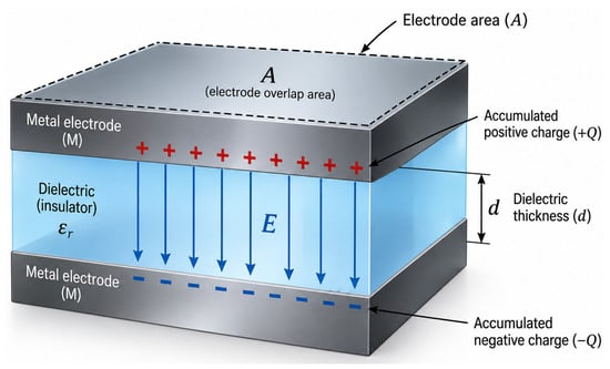
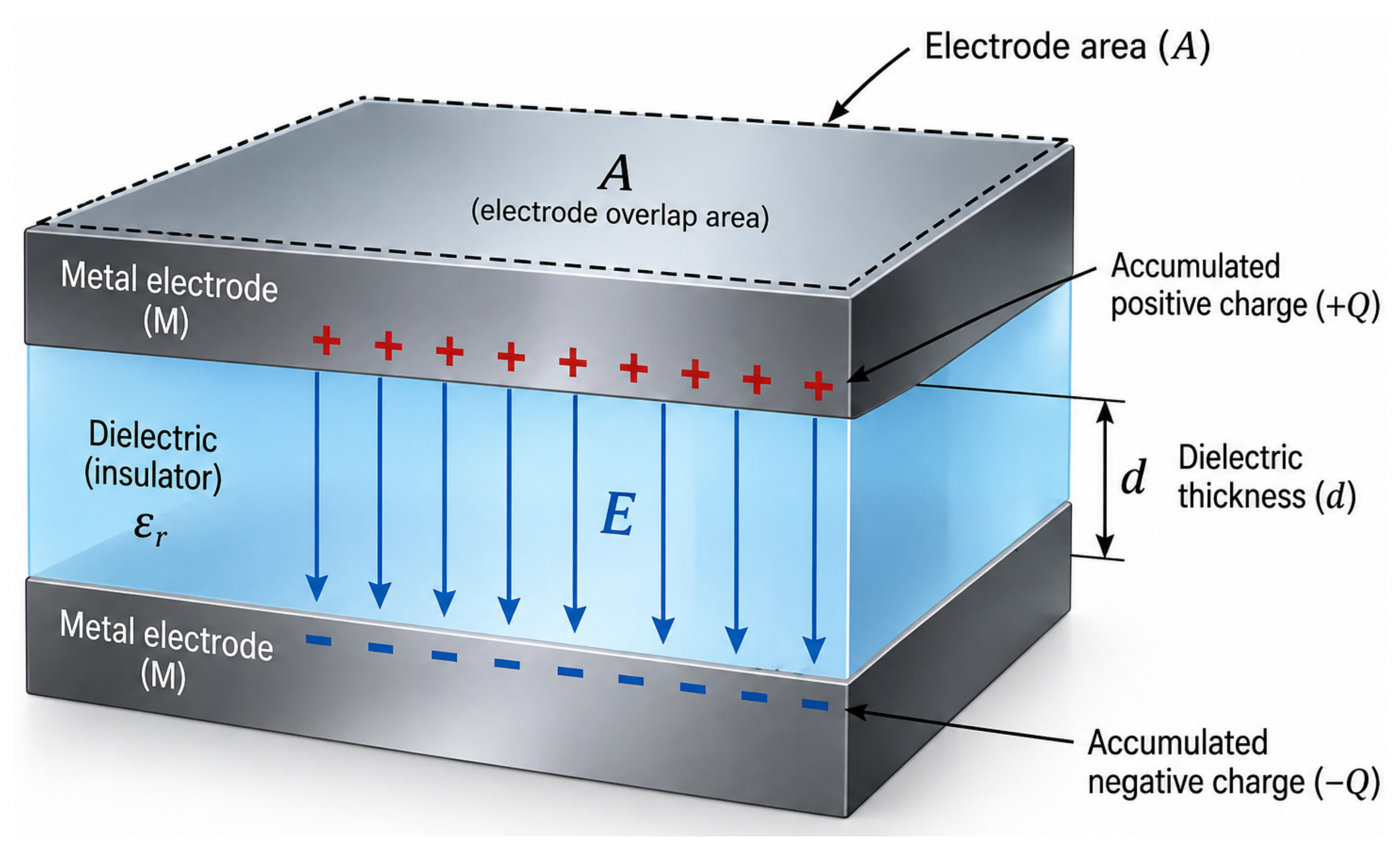
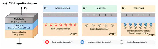
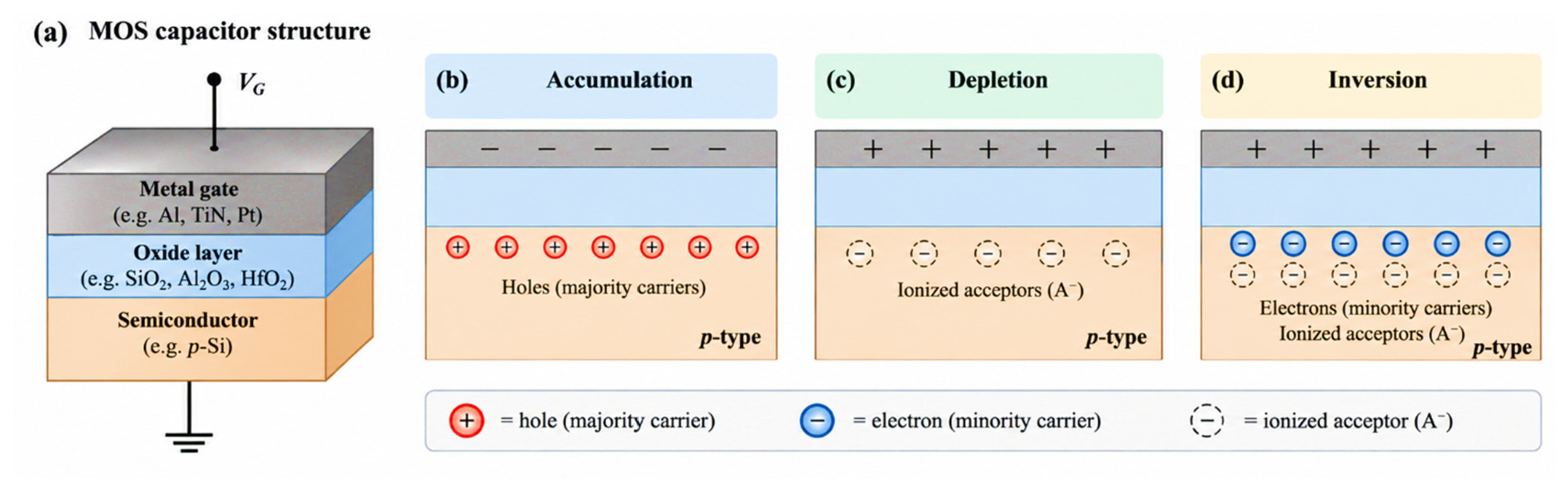
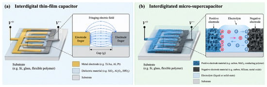
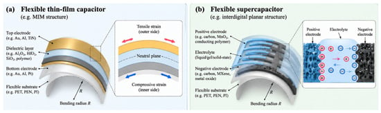
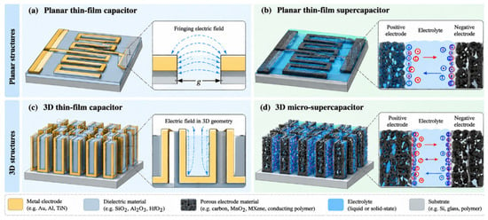
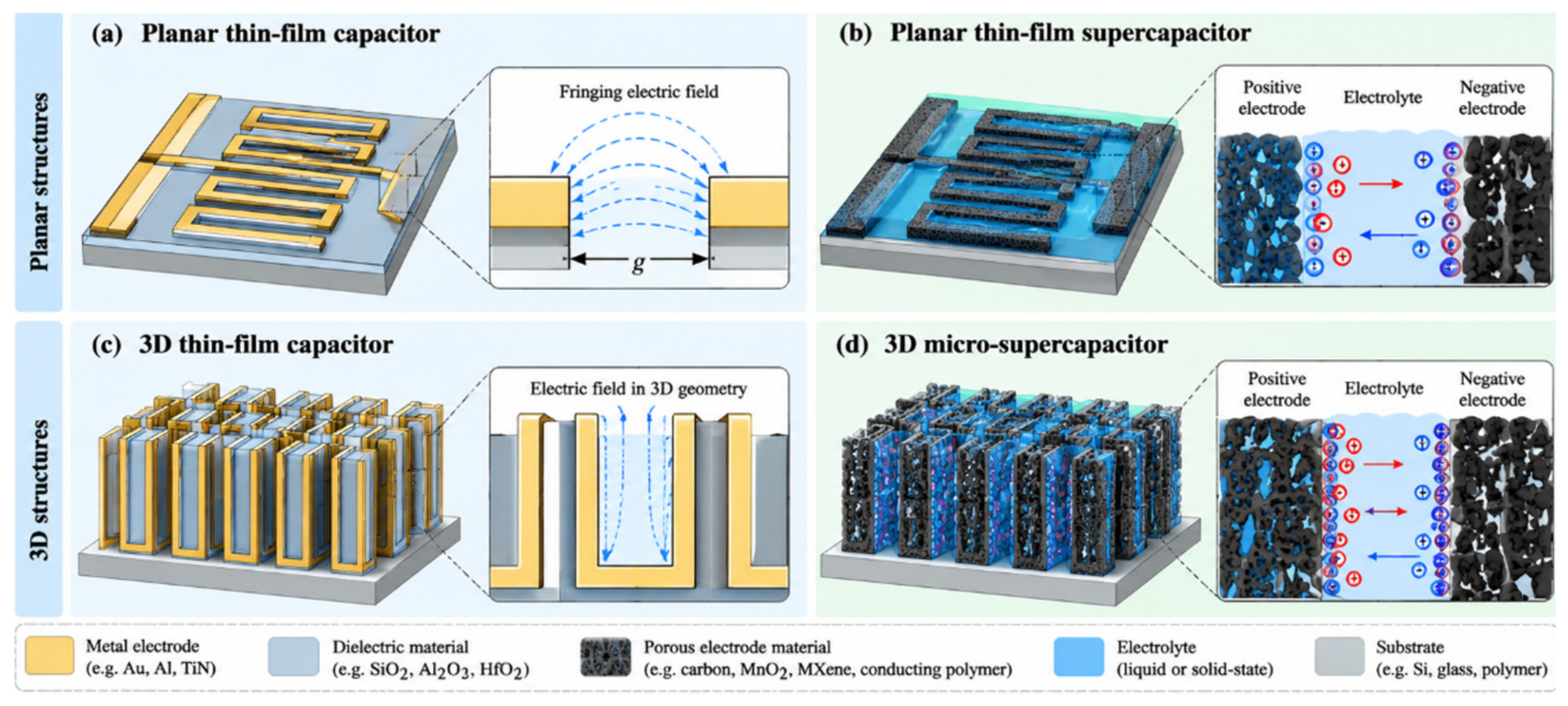

Disclaimer/Publisher’s Note: The statements, opinions and data contained in all publications are solely those of the individual author(s) and contributor(s) and not of MDPI and/or the editor(s). MDPI and/or the editor(s) disclaim responsibility for any injury to people or property resulting from any ideas, methods, instructions or products referred to in the content. |
© 2026 by the authors. Licensee MDPI, Basel, Switzerland. This article is an open access article distributed under the terms and conditions of the Creative Commons Attribution (CC BY) license.