


Abstract
The imperative for EMC-optimized gate drivers in Gallium Nitride (GaN)-based automotive DC-DC converters stems from the stringent CISPR 25 standards and GaN’s intrinsic high-speed switching characteristics, which paradoxically exacerbate electromagnetic interference (EMI). This review distinguishes itself by proposing a novel frequency-domain classification framework (Zone I: <50 MHz for conducted harmonics; Zone II: >50 MHz for switching noise and ringing), which systematically organizes and assesses gate driving techniques against the triad of fundamental GaN EMC challenges: pronounced capacitance nonlinearity, low threshold voltage, and extreme parasitic sensitivity. Unlike prior surveys that primarily catalog techniques, the analysis elevates the gate driver from a simple switch interface to the central “electromagnetic actuator” of the power stage, explicitly elucidating its pivotal role in mediating the critical trade-offs among switching speed, loss, and EMC performance. A comprehensive evaluation and comparison of advanced techniques—from spread-spectrum modulation for Zone I to adaptive current shaping and resonant topologies for Zone II—are provided, alongside an analysis of their design trade-offs. Furthermore, this review presents a first-of-its-kind, phased implementation roadmap towards holistic EMC compliance, integrating intelligent hybrid control, heterogeneous integration, and system-level co-design. This review bridges the gap between device physics and system engineering, offering structured design methodologies and a clear future direction for achieving electromagnetic integrity in next-generation automotive power electronics.
1. Introduction
The global electric vehicle market is experiencing a profound transformation. As illustrated in Figure 1, the global electric vehicle market has experienced remarkable growth, with projections indicating that EVs will soon account for a significant portion of global car sales [1]. It illustrates the growing market demand for automotive DC-DC converters, highlighting the Asia-Pacific region as a key driver. This contextualizes the commercial imperative behind the EMC design challenges discussed in this review. However, this rapid electrification intensifies the challenges of electromagnetic compatibility (EMC) due to the unprecedented density and interaction of electronic components within modern automotive architectures [2]. Consequently, the DC-DC converter, a pivotal component in the vehicle’s power network responsible for stable power delivery, has its electromagnetic behavior under intense scrutiny. Its switching actions are a primary source of conducted and radiated emissions, making it a critical determinant of the overall EMC performance.
Figure 1.
Market Size of Automotive DC-DC Converters in the Asia-Pacific Region and Global Market Distribution by Type (2024).
This review synthesizes and advances the segmented body of existing literature—encompassing wide-bandgap EMI surveys [3], GaN HEMT device analyses [4], fundamental modulation studies [5], and gate-driver circuit implementations [6]—by establishing a unified framework that positions the gate driver as the dynamic regulator at the heart of automotive EMC compliance. To bridge the critical gap between discrete device challenges and system-level performance, it makes three pivotal contributions: (1) the introduction of a novel frequency-domain classification (Zone I/II) to map mitigation strategies to GaN noise characteristics and CISPR 25 limits; (2) the reconceptualization of the driver as a system-level controller that balances switching speed, loss, and emissions; and (3) the formulation of a structured co-design roadmap integrating intelligent control and heterogeneous integration to achieve inherent electromagnetic integrity. Consequently, this work provides a prescriptive, end-to-end methodology for realizing GaN’s full performance potential while ensuring uncompromised EMC resilience in next-generation automotive power systems.
The pursuit of higher efficiency and power density is driving the adoption of wide-bandgap semiconductors, particularly Gallium Nitride (GaN) High-Electron-Mobility Transistors (HEMTs). GaN devices offer superior switching performance, enabling operation at frequencies significantly higher than silicon-based counterparts with minimal loss increase, which allows for a substantial reduction in passive component size and higher power density [7,8,9]. Paradoxically, the ultra-fast switching transitions that enable these advantages also constitute the primary EMC challenge. The resulting high voltage slew rates (dv/dt) generate abundant high-frequency harmonic energy, significantly increasing the risk of non-compliance with stringent automotive EMC standards like CISPR 25, especially in sensitive frequency bands [3,10,11,12].
The gate driver circuit is the critical interface where this conflict is resolved [13]. It translates control signals into precise gate voltage () and current () to regulate the switching trajectory of GaN HEMTs, directly addressing the triad of GaN-specific EMC challenges. As illustrated in Figure 2, the hierarchical logic clarifies the core mechanism: three intrinsic GaN characteristics—pronounced capacitance nonlinearity, low threshold voltage ( = 1–2 V), and extreme sensitivity to parasitic parameters—act as the root causes of EMC issues. The gate driver, as the central control core, mitigates these challenges through dual functions: output voltage/current regulation and switching trajectory shaping (e.g., dv/dt or di/dt suppression). This enables the reconciliation of critical trade-offs between switching speed, power loss, and EMC performance. A high-performance gate driver is indispensable to unleash GaN’s full potential [14]; conversely, a poorly designed driver can amplify EMI risks such as false turn-on and voltage ringing. Ultimately, the driver bridges GaN’s performance advantages with the mandatory CISPR 25 compliance, suppressing conducted/radiated EMI and ensuring electromagnetic integrity.
Figure 2.
Hierarchical block diagram illustrating the core EMC conflict and the pivotal role of gate drivers in GaN-based automotive DC-DC converters.
First, the pronounced nonlinearity of the GaN capacitances, particularly the Miller capacitance (), which exhibits a variation 3–5 times greater with than with Si switches, generates significant displacement currents during switching [15,16]. These currents, intensified by field plates in high-voltage GaN structures, are a primary source of high-frequency ringing and common-mode EMI [17]. Second, GaN’s low threshold voltage ( = 1 to 2 V) naturally increases its susceptibility to dv/dt-induced crosstalk [16]. Experimental validations show disturbances reaching 80% of , leading to false turn-on events that excite >100-MHz oscillations and amplify EMI radiation by over 20 dB [17]. Such false turn-on has been causally linked to a significant proportion of EMI non-compliance cases in GaN-based systems [18,19]. Furthermore, these vulnerabilities are profoundly influenced by parasitic parameters [20,21]. Even minor variations in the PCB layout can dramatically alter parasitic inductance and capacitance, directly impacting the amplitude and frequency of voltage ringing and radiated emissions [22]. Research confirms that parasitic networks readily form resonant circuits prone to high-frequency oscillations, causing significant gate voltage oscillations that risk over-voltage and false switching [20,21,23,24,25,26,27,28,29].
This challenge is further intensified in the unique automotive environment. As shown in Figure 3 and Figure 4, automotive electronic devices share a common chassis ground, where substantial parasitic inductance in the ground return path leads to ground voltage fluctuations [30]. This is critically important for the often-overlooked low-side gate driver, whose reference ground can deviate significantly from the battery negative terminal, complicating its stable operation [31,32]. Ground loop fluctuations exacerbate EMI sensitivity [33], and comparative modeling confirms that GaN transistors generate 37% higher common-mode currents than Si MOSFETs in the 30–100 MHz range [34]. In safety-critical systems such as autonomous driving platforms, electromagnetic noise from power converters can interfere with sensitive sensors and communication buses, making EMC a fundamental functional safety concern, not merely a regulatory hurdle [35].
Figure 3.
GaN-Based Half-Bridge Power Stage High-Side Floating Ground Drive Topology (Conceptual Schematic).
Figure 4.
Generation Mechanism of Common-Mode Interference in High-Voltage GaN Drivers.
The distinction between and in Figure 4 is critical for understanding common-mode (CM) EMI generation. In an automotive chassis, the power ground is theoretically stable but is connected to the driver reference ground through a finite impedance (parasitic , ). During high di/dt switching transients, the current flowing through this impedance creates a voltage difference, or ground bounce (). This bounce directly superimposes a noise voltage on the low-side driver’s reference point. Since the driver’s output voltage () is referenced to this noisy , the integrity of the gate control signal is compromised. Furthermore, this same appears as a common-mode voltage between the converter’s power terminals and the chassis, driving CM currents through parasitic capacitances to earth, which are a major contributor to radiated EMI [30,33]. Therefore, minimizing the impedance between and is a core co-design objective for mitigating CM noise.
While standards like CISPR 25 define the essential emission limits [36], conventional EMC mitigation techniques are often incompatible with GaN device physics. For instance, transition rate moderation via gate series resistance incurs prohibitive trade-offs, including 12–15% switching loss increments that negate GaN’s intrinsic efficiency benefits [7,37]. Therefore, a paradigm shift towards intelligent, EMC-friendly gate driver design is required: a design that dynamically adapts to operating conditions to suppress interference at its source without compromising efficiency. Active mitigation strategies, such as dv/dt-limiting gate drivers and negative-bias circuits, have been shown to reduce false turn-on by over 70% and EMI by 15–30 dB, cementing the gate driver’s pivotal role [38,39,40].
In response to this imperative, this review systematically examines the path toward EMC-friendly gate driver design for GaN-based automotive DC-DC converters. As schematically outlined in Figure 5, our analysis proceeds through a structured framework. Section 2 establishes the theoretical foundation, analyzing the intrinsic GaN EMC challenges and introducing the frequency-domain classification (Zone I: <50 MHz; Zone II: >50 MHz) that guides subsequent technical discussions. Section 3 focuses on gate driver techniques for Zone I, providing a comprehensive evaluation and synthesis of spread-spectrum modulation methods for low-frequency conducted EMI suppression. Section 4 addresses Zone II strategies, analyzing techniques from adaptive gate control to resonant topologies for mitigating high-frequency ringing and noise, concluding with a quantitative summary and comparison. Section 5 bridges theory and practice by analyzing how these principles are embodied in commercial gate drivers, highlighting different co-design philosophies and their system-level trade-offs. Finally, Section 6 synthesizes the conclusions, discusses broader implications, and presents a phased roadmap for achieving EMC-resilient automotive power systems through next-generation, intelligent gate driver design.
Figure 5.
Structural framework diagram of this review article. It demonstrates a systematic exploration of gate drive technologies targeting low-frequency (Zone I) and high-frequency (Zone II) EMI issues, starting from theoretical foundations, culminating in a summary and outlook.
2. Gan’s Intrinsic EMC Challenges and the Gate Driver’s Role: Theoretical Foundation
This section establishes the theoretical cornerstone of this review. We begin by delineating the stringent automotive EMC standards that define the design targets. The core of this section then systematically deconstructs the three fundamental EMC challenges inherent to GaN technology: capacitance nonlinearity, low threshold voltage, and extreme sensitivity to parasitic. We elucidate their physical origins and, critically, demonstrate how these challenges collectively elevate the gate driver to a central position in determining EMC performance. The discussion on near-field radiation further reinforces the imperative for driver-centric optimization.
2.1. CISPR 25 as the Benchmark: The Automotive EMC Compliance Landscape
Automotive electronic systems must operate reliably within complex electromagnetic environments, making compliance with standards like CISPR 25 mandatory [36]. This standard stipulates:
- Emission Limits: It defines the maximum allowable conducted and radiated electromagnetic emissions from electronic equipment during normal operation to prevent interference with on-board receivers and other sensitive devices.
- Immunity Requirements: It specifies the ability of vehicle equipment to withstand external disturbances—such as electrostatic discharge, RF electromagnetic fields, and transient conducted disturbances—without performance degradation or malfunction.
Meeting these limits is particularly challenging for switching converters. As illustrated in Figure 6, the spectrum of a typical PWM converter readily exceeds the CISPR 25 Class 5 limits. The wide input voltage range in automotive applications further complicates this by causing significant spectral drift [11]. Therefore, effective suppression must target the interference at its source: the switching transition governed by the gate driver.
Figure 6.
The conducted EMI spectrum of a typical PWM converter displays measurement results from both peak (PK) and average (AVG) detectors. The gray shaded area represents the CISPR 25 Class 5 limit line, highlighting the risk of exceeding limits within the 76–108 MHz broadcast band.
2.2. Reliability Implications of Poor EMC: Bridging Transient Stress to Device Lifespan
The high-frequency electromagnetic disturbances discussed in the previous sections are not merely a compliance issue but a direct threat to the long-term reliability and operational lifespan of GaN HEMTs in automotive environments. The transient overstress mechanisms inherent to poor EMC—namely voltage overshoot and current ringing, which are exacerbated by the GaN-specific challenges outlined in Section 2.1—accelerate key failure modes in GaN devices [18,19,41].
Electrical Overstress and Gate Degradation: Voltage overshoot at the switching node (), a direct consequence of underdamped parasitic resonance (linked to Challenge III), can routinely exceed the device’s nominal rating. Repetitive exposure to such voltage spikes induces cumulative stress on the gate structure and the AlGaN/GaN heterojunction, leading to time-dependent gate degradation and increased leakage [17,41].
Current Ringing and Interconnect Fatigue: The high-frequency current oscillations (>50 MHz) resulting from false turn-on (Challenge II) and LC resonance cause localized current crowding and elevated electro-thermo-mechanical stress within the device metallization and package interconnects [20,21]. Over millions of switching cycles, this can initiate fatigue failures such as wire bond cracking or solder joint degradation, increasing on-resistance and risking thermal runaway.
Thermal Stress from Switching Losses: Inefficient switching transitions with prolonged ringing directly increase switching losses [27,28]. In high-power-density converters, this aggregates into significant junction temperature rise (). Chronic exposure to elevated temperatures and thermal cycling exacerbates dopant diffusion and trap-related effects, leading to parametric drift or catastrophic failure [29].
Therefore, an EMC-friendly gate driver fulfills a dual role: it is both a spectrum compliance manager and a reliability enabler. By actively shaping the switching trajectory to minimize voltage overshoot, dampen current ringing, and reduce parasitic loss, the driver mitigates the fundamental electrical and thermal stresses that degrade GaN HEMT lifespan. This establishes electromagnetic compatibility not as a standalone design target, but as an integral pillar of functional safety and long-term reliability for automotive power systems [35].
2.3. The Triad of GaN-Specific EMC Challenges and Driver Implications
The power electronics industry has long followed a trend of doubling power density approximately every four years, as shown in Figure 7. This relentless scaling, driven by materials innovation, is the fundamental enabler for system-level miniaturization and efficiency gains [7]. Wide-bandgap semiconductors (WBGs), particularly GaN [42,43], are now at the forefront of pushing these device-level limits, enabling significantly higher switching frequencies and power density compared to silicon [7,44]. However, it is precisely these enabling advantages at the device level—ultra-fast switching and high-frequency operation—that introduce the severe EMC challenges central to this review [45]. Surveys of WBG-specific EMI reduction [46] highlight fundamental differences from silicon-based systems. The superior performance of GaN HEMTs is intrinsically linked to three core physical properties that simultaneously pose severe EMC challenges, fundamentally altering the design priorities compared to silicon-based systems [3,12,22,41,46,47,48].
Figure 7.
Conceptual trend of power density evolution in power semiconductor devices [7,44]. The blue line represents the loop in D, and the red line represents the loop in .
2.3.1. Challenge I: Pronounced Capacitance Nonlinearity and Displacement Currents
The fundamental mechanism stems from the pronounced nonlinearity of GaN’s parasitic capacitances, particularly the Miller capacitance (). As shown in Figure 8, varies dramatically with drain–source voltage (), a change 3–5 times greater than in silicon switches [15]. During high-speed switching, this nonlinearity leads to a large, variable displacement current ( d/dt). This current is a primary source of high-frequency ringing and common-mode EMI [16,17]. Neglecting this nonlinearity can introduce significant errors in loss estimation and undermine circuit stability [18,38].
Figure 8.
Parasitic RLC resonant network model of the gate loop during high-side switch turn-on. The blue line represents the loop in D, and the red line represents the loop in .
These intrinsic device physics impose direct and stringent requirements on the gate driver design [20]. Firstly, the gate driver must source and sink sufficient current to charge and discharge the nonlinear gate capacitance and counteract the injected displacement current, demanding higher peak current capability [20,21,23]. Secondly, the driver is the first line of defense against oscillations excited by this current; its output impedance (e.g., the gate resistance, ) becomes the primary damping mechanism for the resultant resonant networks [24,25,26]. Finally, accurate driver design necessitates models that fully account for capacitance nonlinearity to predict switching behavior and losses correctly, moving beyond simplistic assumptions [27,28,29].
2.3.2. Challenge II: Low Threshold Voltage and dv/dt-Induced Crosstalk
The core of this challenge lies in the interplay between GaN’s low threshold voltage and the high dv/dt transients it enables. GaN’s low threshold voltage ( = 1–2 V) [16] inherently heightens its susceptibility to spurious turn-on events caused by crosstalk from the switching node (). The high d/dt at couples directly to the gate through the Miller capacitance (), creating a disturbance in the gate–source voltage (). GaN HEMTs exposed to dv/dt > 50 V/ns exhibit disturbances reaching 80% of , a vulnerability threefold worse than silicon MOSFETs [16]. The nonlinear interaction between and dv/dt further intensifies this crosstalk [49]. The resultant false turn-on draws a shoot-through current, exciting severe oscillations (>100 MHz) that amplify EMI radiation by >20 dB [17]. Experimental validation confirms this causality: neglecting -dependent crosstalk caused 35% EMI non-compliance in 650-V GaN inverters [18,19].
Figure 9 presents switching node operational waveforms from a dual-phase step-down topology [50]. These waveforms illustrate the rapid switching transitions characteristic of GaN converters. Accelerated switching edges (e.g., / < 5 ns) elevate high-frequency interference energy, particularly between 10–100 MHz. This presents significant electromagnetic compatibility challenges, as evidenced by measured EMI spectra that frequently violate stringent CISPR 25 Class 5 limits, especially in the sensitive 76–108 MHz broadcast band [11]. Recent empirical studies on automotive 48V-12V DC-DC converters confirm that targeted EMI suppression strategies are necessary from the initial design stage.
Figure 9.
Pulse voltage and current conversion waveforms at the switch node of a buck converter.
Consequently, the gate driver transitions from a simple switch to the primary guardian against false triggering. It is the sole component capable of actively preventing false turn-on and must incorporate dedicated features to ensure gate integrity. Essential mitigation strategies implemented at the driver level include applying a negative voltage during the off-state to significantly increase the noise margin [39], integrating a low-impedance path to clamp the gate to the source during off-periods (active Miller clamping), and actively limiting the dv/d through gate current control [38,40]. Such active mitigation techniques have been shown to reduce false turn-on by >70% and corresponding EMI by 15–30 dB [38,39,40], cementing the driver’s role as the critical solution.
2.3.3. Challenge III: Extreme Sensitivity to Parasitic Circuit Elements
The ultra-fast switching edges of GaN devices excite parasitic resonant tanks formed by inevitable PCB and package inductances () and capacitances [20,21]. These underdamped networks lead to high-frequency ringing (>50 MHz), causing gate voltage oscillations that risk over-voltage, false switching, and device failure [20,23,24,25].
This sensitivity forces a paradigm shift: the gate driver and its physical layout must be co-designed as part of the resonant system. As shown in Figure 9, the gate loop itself is an RLC circuit where the driver’s output resistance ( and ) is the primary damping element. The critical damping condition ( (Equation (1)) encapsulates the core trade-off: higher suppresses ringing at the cost of speed and loss [51]. Therefore, minimizing through driver placement and layout is not a secondary step, but a primary EMC design parameter.
2.4. Comparative Perspective: EMC and Driving Challenges of GaN vs. SiC
To fully appreciate the severity of the EMC challenges outlined in Section 2.3.1, Section 2.3.2 and Section 2.3.3, it is instructive to contrast GaN with its primary wide-bandgap rival, SiC. While both technologies enable superior performance compared to silicon, their distinct material properties and device architectures lead to different electromagnetic behaviors, thereby shaping divergent priorities for EMC-optimized gate driver design.
Switching Speed and Edge Rate: GaN HEMTs, owing to their lateral structure and extremely low parasitic capacitances, typically achieve ultra-fast switching transitions [52]. Experimental characterizations report dv/dt rates exceeding 150 V/ns, which can generate significant high-frequency content beyond 100 MHz [53]. In contrast, commercial SiC MOSFETs, while fast, exhibit typical intrinsic dv/dt in the range of 50–100 V/ns under similar conditions, as their switching speed is often limited by different factors such as internal gate resistance and package inductance [54,55]. This notable difference in achievable slew rate means GaN converters inherently push more interference energy into the critical >30 MHz bands where CISPR 25 limits are most stringent [11]. Consequently, the driver’s task of precise edge rate control and mitigation of its side-effects is fundamentally more critical and demanding for GaN.
Threshold Voltage and Robustness: A defining difference lies in the gate structure. Commercial enhancement-mode GaN HEMTs commonly have a low and tightly distributed threshold voltage( ≃ 1–2 V), making them exceptionally susceptible to dv/dt-induced false turn-on as detailed in Challenge II [16,17]. Most SiC MOSFETs employ a Si-MOSFET-like silicon dioxide gate oxide, yielding a higher and more robust typical threshold voltage ( ≃ 2.5–4 V or higher) [56]. This higher intrinsic noise margin reduces crosstalk vulnerability under similar dv/dt conditions, a factor highlighted in comparative studies of phase-leg configurations [57]. This distinction shifts the driver design focus: while negative turn-off bias is beneficial for both, it becomes imperative for reliable GaN operation, whereas for SiC, it is often an option for further optimization or higher safety margin.
Parasitic Capacitance Nonlinearity: Both technologies exhibit nonlinear output capacitances (), but the nature and impact differ. GaN’s Coss variation with is exceptionally steep, and its reverse transfer capacitance () shows significant nonlinearity, resulting in large, variable Miller displacement currents during switching (Challenge I) [15,16]. For SiC MOSFETs, the nonlinearity is also present (a key factor in soft-switching designs) but the nonlinearity may be less pronounced relative to its absolute value, and the Miller plateau during switching is often more distinct [58]. Consequently, GaN drivers must source/sink highly variable peak currents to manage this nonlinear charge, demanding higher bandwidth and more complex modeling [20,23]. SiC driver design, while still advanced, can more frequently rely on simplified quasi-constant current models for initial sizing.
System-Level EMI Profile: These differences lead to distinct EMI spectral profiles and co-design priorities. GaN converters typically exhibit stronger high-frequency emissions due to their higher dv/dt, demanding drivers with precise slew-rate control and layouts optimized for minimum high-frequency parasitics [10,59,60]. In contrast, while SiC designs also require careful layout, their EMI management often involves a broader strategy addressing both high- and lower-frequency harmonics.
The key distinctions are summarized in Table 1 below.
Table 1.
Comparison of Performance Between GaN and SiC.
This comparison underscores that while both GaN and SiC necessitate advanced gate drivers compared to traditional Si, the EMC challenges for GaN are uniquely intensified by the confluence of the highest achievable switching speeds, the lowest threshold voltage, and pronounced capacitance nonlinearity. These factors collectively demand a gate driver that acts as a high-bandwidth, adaptive actuator with robust protective features. Therefore, the paradigm shift towards intelligent, EMC-optimized gate drivers—capable of adaptive current control, active protection, and intimate system co-design—is not merely beneficial but essential for GaN to meet automotive-grade reliability and compliance standards. The subsequent sections of this review will delve into the specific techniques developed to address this GaN-specific imperative.
2.5. Near-Field Radiation: A System-Level Consequence of Switching Dynamics
In the confined spaces of automotive electronics, near-field radiation, induced by high di/dt and dv/dt in switching nodes and loops, holds significant importance [61]. Even when far-field radiation meets standards [62], near-field coupling can disrupt the operation of adjacent sensitive circuits like sensors and communication modules.
The GaN-Specific Challenge: The high dv/dt and di/dt associated with GaN switching result in significantly stronger near-field radiation compared to silicon-based systems, posing a major challenge for electromagnetic co-existence in densely packed automotive electronics [60,61].
The Gate Driver’s Role: Crucially, the intensity of these near-field sources is directly governed by the slew rates and ringing amplitudes controlled by the gate driver. Therefore, driver strategies that effectively reduce ringing and provide controlled slew rates are key to mitigating near-field coupling [63,64].
2.6. Conclusion of Theoretical Foundation
When dealing with EMC problems, three key elements need to be focused on: the electromagnetic interference source, the coupling path, and the sensitive equipment. The electromagnetic interference source is the root cause of the problem. The coupling path determines how the interference spreads, while the sensitive equipment is vulnerable to the influence of the interference. The sources and coupling paths of EMC problems in DC-DC converters for automotive electronics are discussed before. These factors may make it difficult for the module to meet the requirements of the CISPR 25 standard.
The 50 MHz demarcation is motivated by both regulatory and physical considerations. Regulatory standards like CISPR 25 impose stringent limits above 30 MHz, particularly in critical bands like 76–108 MHz [36]. Physically, the EMI spectrum of GaN converters shows a distinct transition around this frequency: below 50 MHz, discrete switching harmonics dominate; above 50 MHz, broadband noise and ringing from fast switching edges and parasitic resonances prevail [11,34]. This aligns with the core challenges: lower harmonics relate to the fundamental switching action, while high-frequency content is directly tied to dv/dt-induced displacement currents (Challenge I) and underdamped parasitic resonances (Challenge III).
Based on the analysis in these two parts, we identify the two nodes, and , and classify the EMC problems accordingly. As shown in Figure 10, they are separated by an operating frequency of 50 MHz. This figure introduces the core frequency-domain segmentation framework (Zone I/II) of this review, which organizes subsequent technical discussions and provides a targeted design roadmap. In Zone I, the EMC problem is caused by the distribution of the EMI spectrum at and harmonics. In Zone II, the EMC problem is caused by pseudo-ringing at and rapidly changing current voltage. Therefore, to solve the EMI, noise, and ringing problems of the overall circuit, the methods of zone I and zone II should be different and targeted respectively.
Figure 10.
A segmented framework for addressing EMC issues in DC-DC converters for automotive electronics. Based on interference source nodes ( and ) and frequency ranges (with 50 MHz as the boundary), EMC challenges are categorized into Zone I (dominated by switching harmonics) and Zone II (dominated by switching ringing and dv/dt). This provides a clear design roadmap for subsequent targeted solutions.
The analysis presented in this section unequivocally demonstrates that the core EMC challenges in GaN-based converters—stemming from nonlinear capacitances, low threshold voltage, and parasitic sensitivity—are not merely system-level concerns but deeply rooted in the switching transient controlled by the gate driver. The driver is no longer a simple on/off switch but the critical actuator for managing the electromagnetic behavior of the power stage. The subsequent sections of this review will, therefore, focus on the advanced gate driver techniques that have been developed specifically to address this triad of challenges, enabling compliance with automotive EMC standards without sacrificing the performance advantages of GaN technology.
3. Gate Driver Techniques for Low-Frequency EMI Suppression (Zone I)
Building upon the frequency-domain framework established in Section 2, this section critically examines gate driver strategies dedicated to Zone I (<50 MHz). The analysis will transcend a mere enumeration of spread-spectrum techniques by evaluating them through the lens of spectral management efficacy. Key comparative dimensions will include the pattern of frequency modulation (fixed/periodic vs. random), its impact on output regulation, and the inherent trade-offs between EMI attenuation depth and system complexity. This structured comparison aims to distill practical selection guidelines tailored to the constraints of automotive GaN converters.
This section addresses the suppression of conducted electromagnetic interference (EMI) below 50 MHz (Zone I), a critical frequency range governed by automotive standards like CISPR 25. The energy in this zone is predominantly concentrated at the switching frequency () and its harmonics. We establish that the root cause of this low-frequency EMI stems from the periodic, sharp switching transitions governed by the gate driver, which excite the nonlinear capacitances (Challenge I) of GaN HEMTs and are susceptible to disruptions from phenomena linked to their low threshold voltage (Challenge II). Consequently, the core strategy for EMC-friendly gate driver design in this domain shifts from merely executing on/off commands to intelligently modulating the switching frequency or timing, as shown in Figure 11. This “macro-control” approach aims to spread the concentrated harmonic energy in the frequency domain, thereby reducing peak amplitudes and ensuring compliance, without fundamentally altering the nanosecond-scale switching edges that define GaN’s performance.
Figure 11.
Zone I EMC Suppression Technology Classification Diagram: A technology roadmap centered on Spread Spectrum Modulation (SSM) and its variants. It emphasizes strategies for suppressing low-frequency conducted EMI through macro-frequency.
3.1. The Genesis of Low-Frequency EMI and the Imperative for Driver-Centric Control
The spectral signature of Zone I EMI, characterized by discrete, high-amplitude harmonics at the switching frequency and its multiples, is a direct manifestation of the periodic switching actions governed by the gate driver. Its generation, however, is fundamentally rooted in the specific physical properties of GaN devices. The primary mechanism stems from Challenge I (Pronounced Capacitance Nonlinearity): the rapid, gate-driver-controlled current and voltage transitions energize the highly nonlinear junction capacitances (notably and ), converting the sharp time-domain edges into rich harmonic content in the frequency domain [15,16]. This inherent harmonic generation is further exacerbated by phenomena linked to Challenge II (Low Threshold Voltage): any spurious current spikes resulting from dv/dt-induced false turn-on events inject additional high-frequency noise into the power loop, adding to the harmonic amplitude, particularly at lower-order multiples of the switching frequency [17]. Consequently, while the root cause is the fixed-period switching clock, the amplitude and characteristics of the resulting Zone I EMI are directly amplified by GaN’s intrinsic challenges. Therefore, an EMC-friendly gate driver for this domain must evolve beyond a simple clock provider to become a “spectral manager,” employing intelligent modulation strategies to disperse this challenge-amplified harmonic energy without altering the fundamental nanosecond-scale switching edges that define GaN’s performance.
Therefore, an EMC-friendly gate driver for Zone I must evolve into a “spectral manager.” Its primary function expands to include the intelligent modulation of the switching period. The objective is to redistribute the harmonic energy over a wider frequency band, effectively lowering the peak spectral density below regulatory limits. This paradigm represents a form of “macro-control” exerted by the driver, targeting the frequency-domain manifestation of the underlying device physics challenges, rather than directly damping the high-frequency ringing (Challenge III) associated with individual switching events.
3.2. Spread Spectrum Modulation: The Core of an EMC-Friendly Driver’s Arsenal
Spread Spectrum Modulation (SSM) stands as the principal technique for gate drivers to implement this spectral management. Its fundamental principle involves deliberately varying the switching frequency () within a defined bandwidth (). According to Carson’s law, while the total emitted power remains constant, the energy originally concentrated at discrete harmonics is spread, leading to a significant reduction in peak amplitudes [5,65,66,67].
3.2.1. Basic Principles and Typical Cases of SSM Technology
Spread Spectrum Modulation (SSM) operates on the core principle of deliberately varying the switching frequency () within a defined bandwidth (). This spreads the concentrated energy at the switching frequency and its harmonics into a broader, continuous spectrum, thereby reducing peak amplitudes to comply with conducted EMI limits.
A classic implementation is the Pseudo-Noise Compression (SNC) method [5], whose operating principle is illustrated in Figure 12.
Figure 12.
Block diagram of the Pseudo-Noise Compression (SNC) clock generator [5]. The circuit introduces time-domain jitter within a triangular wave envelope via a noise source (e.g., Zener diode), randomizing the switching frequency to flatten EMI spectrum peaks.
Its core principle is to randomize the switching instant by modulating a reference voltage with a combination of a low-frequency envelope and broadband noise, which is then compared against a fixed ramp to generate a frequency-jittered clock signal. This process spreads discrete harmonics into a continuous spectrum, typically achieving 10–15 dBµV peak EMI attenuation. However, the performance of SNC is limited by the quality of the physical noise source and can lead to output voltage jitter. This motivates more advanced digital modulation schemes.
The evolution of SSM continues, with modern implementations leveraging advanced digital signal processing techniques like sigma-delta modulation to achieve more precise spectral shaping and even concurrently mitigate common-mode noise [68,69]. According to Carson’s law, the total power remains unaltered. Originally, the high EMI spikes concentrated around and its harmonics (N) are now compressed over a wide frequency range, effectively diminishing EMI. Consequently, the spurious noise floor is lowered beneath the EMI standard.
The SSM is not confined to the method presented in [5]. Nevertheless, current SSM solutions each come with their own set of problems. Fundamentally, there exists a trade-off between the extended range of the switching frequency and the SSM modulation frequency . In order to achieve substantial EMI suppression, it is necessary to configure a larger and a smaller . On the one hand, while a broader can assist in compressing spurious noise across a wide frequency band, it simultaneously heightens the likelihood of spectral overlap between adjacent harmonics [70], thereby undermining the EMI improvement efforts. More pronounced EMI spikes cannot be mitigated by the so-called “matryoshka” SSM approach (a technique that employs nested modulation patterns). On the other hand, directly impacts the modulation slew rate of SSM. In both the fixed slew rate scenario [71] and the Random SSM mechanism [72], the value of remains unregulated. Consequently, a fixed has to be employed to avert potential overlapping spikes, which in turn limits the efficiency of such SSM methods in resolving EMI issues. Phase-aligned EMI adaptive self-cancellation [70] reduces CISPR 25 violations 82% via BER-conscious control. Condition-adaptive schemes [73,74] dynamically optimize modulation envelopes during transients, while random frequency hopping [75] and Markov-chain RSSM [76] achieve 35 dBV attenuation through entropy maximization. It is crucial to note that the effectiveness of any SSM strategy is contingent upon the specific power stage characteristics. As shown in [77], the attenuation achievable for a given and can vary significantly depending on the converter’s operating point and load conditions. To sum it up, for better EMI mitigation, the SSM method demands as large a as possible while also addressing problems like spectral overlap that arise from a larger . Additionally, the modulation effect of will directly bear on the attainable range of .
3.2.2. Resolving Spectrum Overlap
A fundamental constraint in SSM design is the risk of spectral overlap, where enlarging the modulation depth () for greater suppression can cause adjacent harmonics to interfere, generating new peaks. Advanced SSM variants address this through distinct strategies, as compared in Table 2.
Table 2.
Comprehensive comparison of Zone I (<50 MHz) EMI suppression techniques.
Multi-Rate SSM (MR-SSM) techniques [73,74,78] employ an adaptive, deterministic approach. The core idea is to dynamically adjust the upper and lower modulation sidebands () in response to system conditions such as input voltage () or load. This intelligent adjustment prevents the fixed modulation pattern of basic SSM from guaranteeing overlap across varying operating points. Ref. [78] adopts indirect modulation by actively controlling the turn-on time () and adaptive synchronization off-time. This approach extends the SSM frequency range without generating EMI aliasing spikes. As illustrated in [78], the switching frequency is modulated in the frequency domain, leading to a non-fixed swing rate. A lower swing rate of corresponded to a broader spread, reducing its occurrence in the time domain. Consequently, the EMI energy carried by this frequency component and its associated harmonics is suppressed, achieving directional redistribution of EMI energy and eliminating EMI power aliasing spikes. However, this method is only capable of performing center-spread modulation, and the up and down sidebands could not be independently controlled. Moreover, since it operates based on a preset , it could not optimize the EMI performance in the same way as Random SSM. In comparison with [78], Refs. [73,74] not only enhanced the adaptability of to the input voltage and output load but also regulated the sidebands of the up and down according to the input voltage.
A conceptual implementation of this adaptive control is illustrated in Figure 13. This architecture retains the PWM comparator core—common to the basic SNC generator (Figure 12)—comprising the adder, fixed-slope ramp generator, and high-speed comparator. Its pivotal innovation, however, is the addition of an intelligent feed-forward control path. This path senses operational parameters such as the input voltage () and, through an adaptive algorithm, dynamically adjusts the modulation envelope (e.g., the amplitude or offset of the triangular wave) to generate a condition-optimal reference voltage . Consequently, the role of the “noise” and “DC bias” components—central to Figure 12—is supplanted by deterministic, intelligent decision-making; they are merged and marked as “Optional” in this diagram, indicating their demotion from the design backbone to auxiliary elements. Thus, Figure 13 visually encapsulates the evolution of the design philosophy from “introducing uncontrolled randomness” (Figure 12) to “executing predictable, condition-optimal control.”
Figure 13.
Block diagram of the adaptive Multi-Rate SSM (MR-SSM) controller [73,74]. This architecture evolves from the basic SNC structure by integrating an intelligent feed-forward path for condition-aware modulation, while retaining the core PWM comparator stage. The traditional noise and bias components are relegated to an optional role.
The TR-SSM modulation scheme proposed in [79] takes a distinct approach to resolving spectral overlap compared to [73,74,78]. It also exhibits a degree of randomness and flexibility reminiscent of that in [67]. The implementation pathway is depicted in Figure 14. It enhances the randomization foundation by replacing the analog noise of Figure 12 with a robust digital True Random Number Generator (TRNG). Furthermore, it evolves the principle of path separation seen in Figure 13, applying it to create two independent, specialized randomization paths (high-frequency and low-frequency). The outputs of these paths are combined and then processed by the same core PWM comparator stage inherited from Figure 12 and Figure 13. This design effectively generates complex, non-periodic frequency jitter, achieving superior dispersion of harmonic energy and minimization of spectral overlap.
3.2.3. The Modulation of
It has also been addressed more flexibly in recent years, and many works have proposed more versatile Random SSM schemes. Early periodic SSM (PSSM) was intuitive and easy to implement, but the EMI suppression was not satisfactory [80]. Random SSM (RSSM) outperforms PSSM with lower peak EMI and nearly uniform noise spread, but its performance is highly dependent on the random clock design. Random clocks are designed in two ways: discrete and continuous.
To implement RSSM in circuits, many works use digital random clock generators to discretely randomize the switching frequencies of converters, such as in [81]. Theoretically, the reduction in EMI has a logarithmic relationship with the number of discrete modulation frequencies used in the circuit [82]. For the N-bit digital random clock designed in [81], to achieve satisfactory EMI suppression, the number of bits N must be large. Otherwise, the frequency resolution will be rather limited, and the EMI suppression effect will be poor. Achieving greater EMI suppression demands a large number of digital circuit modules, which pose high requirements for power consumption, cost, and design complexity.
Figure 14, however, the TR-SSM modulation scheme proposed in [79] reduces the requirement for N through dual-channel modulation. The low-frequency modulation path is a random digital modulation of . RN<0:7> is delayed to obtain RNLF<0:7>, which is used to randomize the low-frequency clock signal with a frequency of 1/. Subsequently, the low-frequency ramp signal and the clock signal are obtained. Compared with the modulation system in [81], TR-SSM ensures that the random code of low-frequency SSM is uncorrelated with the current random code but depends on the previous one, thus achieving better entropy. This property makes the modulation process more random and unpredictable, helping to break the correlation between harmonics and further optimize EMI performance by reducing potential interference peaks.
Referring to [81], Ref. [79] can be considered to directly give a definite value of N, and Ref. [79] does not require a large value of N. The reason lies not only in the fact that low-frequency SSM and high-frequency SSM each modulate the switching frequency in a random and independent manner but also in the fact that the finally generated is the sum of the two. The superposition of randomness reduces the requirement for N. The selection of the value of N needs to comprehensively consider actual requirements and design complexity. Integrated bootstrap charge balancing in TR-SSM [83] stabilizes high-voltage floating drives while ensuring full-band CISPR 25 compliance. Markov-chain-based continuous RSSM [76] demonstrates superior entropy properties, achieving 35 dBV EMI attenuation through optimized randomness. The biggest drawback of TR-SSM is that the complex interactions and signal processing among multiple modules increase the complexity of the circuit structure. Dual-channel modulation means that the modulation processes of both the high-frequency and low-frequency bands need to be precisely controlled and coordinated simultaneously. This includes ensuring that the random codes of the two bands are independent of each other and have appropriate correlations, as well as adjusting the switching frequencies of the two bands within an appropriate range to achieve effective harmonic mitigation. All of these greatly increase the complexity of circuit implementation and control for the system.This complexity is a recognized focus of ongoing research, with the overarching goal being the development of adaptive gate drivers that achieve an optimal trade-off between switching speed, loss, and EMI across a wide range of operating conditions [84].
To achieve near-ideal RSSM, a cost-effective continuous RSSM (C-RSSM) is highly desirable. The approach in [72,85] utilizes an analog circuit implementing a Markov-chain-based chaotic signal generator. The specific implementation process is shown in Figure 15. This circuit produces a continuously random output voltage, which is then used to modulate the voltage-controlled oscillator (VCO) input. This method enables truly continuous and random variation of the switching frequency within the desired sidebands, approaching the ideal spread-spectrum characteristic for superior EMI suppression.
Figure 15.
Circuit implementation of the Continuous Random SSM (C-RSSM) from [72,85]. This circuit employs a Markov chain-based analog chaotic signal generator to produce continuous random outputs in an analog manner, thereby achieving continuous modulation within the sidebands of the center frequency and obtaining near-ideal EMI suppression performance.
RSSM has achieved remarkable results in EMI suppression. However, the circuit design and implementation of RSSM are more complex. Moreover, the continuously random complicates the regulation of another important performance parameter, , in DC-DC power converters. If a traditional feedback regulation circuit is used to regulate in RSSM, significant jitter will occur. Beyond control loop innovations, topological choices can inherently alleviate these challenges. Multilevel converters [86] and innovative inverter topologies [76] naturally reduce the dv/dt and di/dt stress on individual switches, thereby diminishing the source of high-frequency ringing and easing the burden on the gate driver. To achieve strict regulation, specific control circuits, such as ramp compensation circuits [87], are required, which consume more power, take up more area, and have relatively large loop response lags due to limited loop gain bandwidth. The ITR technique [76] resolves this via instantaneous duty-cycle tracking, whereas [88]’s digital random clock reduces jitter by 27.6 dB. For voltage-mode converters, ramp compensation [89] remains limited. The improvement brought by [87] is also very limited, and this solution is only applicable to voltage-mode converters. Ref. [85] proposed a technique named 1TR, which introduces a fast tracking path. By detecting the instantaneous duty cycle D and the switching frequency, it can synchronously modulate the on-time with the jitter of , stabilize the duty cycle, and effectively eliminate the output voltage jitter.
The modulation of in [73,74] does not fall into any category of RSSM. However, it is a relatively advanced modulation technique and can be regarded as an auxiliary method that can cooperate with other EMI suppression techniques to dynamically optimize the EMI performance of the entire system under different working conditions. The envelope tracking technology of proposed in [73,74] allows to make a small adaptive adjustment following the load current on the premise of meeting the CISPR 25 standard. Its core lies in creating a hysteresis window for . Changes in the load current will be reflected on the slope of through a capacitor, altering the timing of reaching the hysteresis limit and triggering subsequent circuits. Nevertheless, it lacks slew rate control during the turn-on and turn-off of the switch, which is somewhat less than ideal.
3.3. Loop Filter and Canceller (LFC) Technique
The LFC (Loop Filter and Canceller) technique [79] exemplifies an active noise cancellation approach. It actively senses and injects a compensating signal to cancel EMI noise in the power path. A critical aspect of its performance is its dependence on a stable ground reference. Ground bounce (), caused by high di/dt transients in the power stage, can directly interfere with the cancellation signal’s accuracy. Therefore, achieving low parasitic inductance in the PCB layout, particularly for ground connections shared between the power stage and the driver/canceller circuitry, is essential for LFC’s effectiveness.
3.4. Synthesis: Reconciling Zone I Techniques with the Triad of Challenges
Having dissected individual Spread Spectrum Modulation (SSM) techniques and their circuit implementations, this section synthesizes the findings into a coherent design framework. The primary challenge in Zone I is navigating the multi-dimensional trade-off between EMI suppression depth, output regulation stability, implementation complexity, and operational adaptability.
To provide a high-level overview of this trade-off space, Figure 16 summarizes the evolutionary generations of Zone I EMI suppression techniques, comparing their typical suppression performance against implementation maturity. This visual summary serves as an intuitive guide for initial technology screening, highlighting the progression from basic filtering to advanced intelligent modulation.
Figure 16.
Summary of gate drive technology characteristics for low-frequency EMI suppression (Zone I). Key parameter characteristics of different spread-spectrum modulation techniques are compared to provide an intuitive reference for technology selection.
To further clarify the architectural evolution, Figure 17 presents a taxonomic overview of the SSM techniques specifically, mapping the relationship between core design philosophies and their concrete circuit embodiments.
Figure 17.
Taxonomy and architectural evolution of Spread Spectrum Modulation (SSM) techniques for Zone I conducted EMI suppression.
As illustrated in Figure 17, the evolution bifurcates into two distinct philosophical paths: the deterministic, condition-aware optimization (exemplified by MR-SSM) and the pursuit of higher-quality stochasticity (evolving from SNC to C-RSSM). This high-level map reframes the gate driver’s role from a passive switch activator to an active spectral architect, responsible for choosing and implementing the appropriate randomization strategy.
To translate the architectural overview into practical design guidance, Table 2 provides a detailed, side-by-side comparison of all key Zone I EMI suppression techniques discussed, including their associated gate driver implications.
The synthesis in Figure 17 and Table 2 underscores a pivotal trend: advancing EMI performance in Zone I invariably increases the gate driver’s intelligence, complexity, and system integration depth. The choice is not linear but strategic:
- The stochastic path (SNC → C-RSSM) seeks ultimate performance but transfers the design challenge to managing output integrity and randomness quality.
- The deterministic path (PSSM → MR-SSM) prioritizes controllability and stability, seeking sufficiency through intelligence.
Therefore, the selection of a Zone I strategy is fundamentally a system-level decision. It must consider not only the EMI spectrum but also the converter’s regulation requirements, available board area, computational resources, and the gate driver’s capability to act as a coherent spectral actuator. This transition from discrete circuit techniques to a holistic control philosophy completes the redefinition of the gate driver for the GaN era. It also sets the stage for the subsequent discussion on Zone II (>50 MHz), where the driver must evolve further into a high-speed analog controller to manage switching-edge-induced noise at its source, confronting a different yet equally critical facet of the EMC challenge.
4. Gate Driver Techniques for High-Frequency Ringing and Noise Control (Zone II)
Transitioning to the high-frequency domain (Zone II, >50 MHz), this section analyzes gate driver techniques designed to mitigate switching-node ringing and noise at their source. The focus here shifts from macro-frequency management to micro-level switching trajectory shaping. We will organize the review along an evolutionary pathway: from passive damping via gate resistance, through adaptive digital control, to advanced active current shaping and resonant topologies. Each category will be assessed on its ability to address the specific GaN challenges—particularly parasitic sensitivity (Challenge III) and capacitance nonlinearity (Challenge I)—while managing the fundamental speed–loss–EMC trilemma.
This section addresses the critical challenge of suppressing electromagnetic interference in the high-frequency domain (Zone II, >50 MHz), where switching-node ringing, voltage overshoot, and near-field radiation present fundamental barriers to automotive EMC compliance. These disruptive phenomena emerge from the convergence of GaN’s intrinsic challenges: nonlinear capacitance interacting with parasitic circuit elements to form underdamped resonant tanks, while the low threshold voltage enables destructive false turn-on events. As shown in Figure 18, the EMC-friendly gate driver must therefore evolve beyond simple switching functions to become an intelligent controller capable of real-time trajectory shaping layout parasitic parameters.through sophisticated current management techniques.The technical route summarized in Figure 19. It visually demonstrates the fundamental trade-off in Zone II: increasing gate resistance suppresses dv/dt and ringing but at the direct cost of extended switching time and higher losses, framing the core design challenge. The properties in this section are organized in Figure 20.
Figure 18.
Effect of Gate Resistance Adjustment on Rise Phase. This clearly demonstrates how increasing gate resistance effectively reduces the voltage rise rate (dv/dt) and suppresses ringing, but this comes at the cost of increased switching time and switching losses.
Figure 19.
Zone II EMC Suppression Technology Classification Diagram: A technology roadmap centered on gate resistance control. The technologies are systematically categorized into three generations: from fixed direct resistance adjustment, to indirect current shaping, and finally to advanced topologies such as resonance and energy recovery. This progression reflects the evolution from passive suppression to active, intelligent control.
Figure 20.
PerformanceComparison Chart of Gate Drive Technologies for High-Frequency Ringing and Noise Control (Zone II). Qualitatively describes the trade-off between ringing suppression rate and achievable minimum parasitic inductance across different technologies. System-in-Package (SiP) and auxiliary tube technologies demonstrate optimal overall performance, while direct resistor adjustment methods are severely constrained by layout parasitic parameters.
4.1. Technical Evolution: From Programmable Resistance to Intelligent Current Control
The disruptive high-frequency phenomena in Zone II—switching-node ringing, voltage overshoot, and intense near-field radiation—emerge from the confluence and interplay of all three GaN-specific challenges. Challenge III (Extreme Parasitic Sensitivity) provides the necessary underdamped resonant tanks formed by PCB and package parasitics. Challenge I (Pronounced Capacitance Nonlinearity), specifically through the Miller capacitance (), acts as the primary coupling mechanism, injecting high dv/dt-driven displacement currents that excite these parasitic networks [16,17]. Simultaneously, Challenge II (Low Threshold Voltage) lowers the immunity threshold, allowing the resulting high-frequency oscillations on the switching node to couple back to the gate, potentially causing catastrophic false turn-on events that further energize the resonant loop [18,19]. This triad creates a vicious cycle where parasitics enable oscillation, nonlinear capacitance drives it, and low exacerbates it. Therefore, gate driver techniques for Zone II must perform a multifaceted intervention: they must provide damping to address parasitic resonance (Challenge III), control slew rates (dv/dt) to manage displacement current injection (Challenge I), and ensure gate integrity through clamping or negative bias to prevent spurious triggering (Challenge II). The evolutionary path from programmable resistance to intelligent current control represents the pursuit of more integrated and effective ways to simultaneously break this cycle at multiple points.
The evolutionary path for EMC-friendly gate drivers in Zone II applications represents a fundamental transition from static configuration to dynamic, intelligent control of the gate current ()—the fundamental parameter governing GaN HEMT switching behavior. This progression reflects increasing sophistication in managing the core trade-off between switching speed and electromagnetic compatibility.
4.1.1. Programmable Gate Resistance: The Foundation of Adaptive Control
Programmable gate resistor arrays provide a digitally adjustable means to dynamically control the gate loop’s damping characteristic, addressing parasitic sensitivity (Challenge III) [20]. The core adjustment mechanism of this technique is a digital selection network, as conceptually illustrated in Figure 21. By offering a range of selectable resistance values, they enable optimization after PCB layout finalization to approach critical damping conditions [51,90], as shown in Figure 22. This allows for adaptive tuning during operation—for instance, implementing lower resistance for minimal turn-on delay and higher resistance during the Miller plateau to control dv/dt and displacement currents (Challenge I). However, this method represents a direct trade-off: selecting conservative resistance values to ensure stability across variations inevitably sacrifices switching speed and increases switching losses by 12–15% in typical implementations [91]. Its effectiveness remains highly dependent on the specific parasitic profile, requiring meticulous characterization for different GaN devices and layouts [92,93].
Figure 21.
Core adjustment mechanism of a programmable gate resistor array: digital selection of a discrete resistance value ().
Figure 22.
Conceptual circuit diagram of a variable gate driver with a programmable resistor array. This structure represents a direct control approach, dynamically adjusting gate drive strength by digitally switching discrete resistors to achieve a trade-off between switching speed and ringing suppression.
4.1.2. Advanced Current Shaping: The Path to Intelligent Control
Advanced current shaping techniques represent a paradigm shift beyond resistive control, employing active current management to achieve superior EMC performance through precise gate current waveform control. Segmented driving implements temporal intelligence by dynamically adjusting the gate driver’s output strength within a single switching transition [90,94,95]. A typical implementation employs a strong pull-up current (low effective ) for initial charge transfer to minimize delay, then automatically switches to a weaker current (high ) specifically during the Miller plateau region. This phase-targeted control allows for precise management of the drain–source voltage slew rate (d/dt), thereby directly mitigating the displacement currents induced by nonlinear capacitances (Challenge I) and providing tailored damping for resonant transients. This is achieved through its core adjustment mechanism: a timed switching between multiple current sources, depicted in Figure 23. Figure 24 shows the flow diagram of the digital control loop in [96]. This is also a specific implementation of the ’R-2R Ladder or Discrete Resistors’ shown in Figure 21. This system actively senses switching node ringing or overshoot, processes the feedback through digital control logic, and dynamically adjusts the gate driver’s configuration (e.g., drive strength) to suppress the oscillations in real time.
Figure 23.
Core adjustment mechanism of a segmented gate driver: time-sequenced switching between strong and weak current sources.
Figure 24.
Functional block diagram of the closed-loop gate ringing suppression system based on [96].
The current-source gate driver (CSD) architecture represents a more fundamental advancement by replacing the conventional voltage-source-with-series-resistance model with controlled current mirrors that deliver a precisely defined gate current () [97]. Its key innovation, shown in Figure 25, is the use of a high-output-impedance current mirror as the core adjustment mechanism. This approach offers inherent immunity to the destabilizing effects of parasitic gate inductance (Challenge III) through direct current control rather than voltage regulation. Consequently, it enables sub-nanosecond transition control while maintaining stability across layout variations, achieving switching performance superior to purely resistive approaches.
Figure 25.
Core adjustment mechanism of a current-source driver (CSD): a high-output-impedance current mirror regulating gate current ().
The most sophisticated approach employs magnetic coupling and closed-loop dv/dt control, implementing a comprehensive sensing and compensation system where miniature magnetic coupling sensors directly detect Vds dv/dt without introducing parasitic capacitance [98]. The operational principle utilizes a compact magnetic core positioned to sense the displacement current proportional to dvds/dt, with the sensed signal fed to a high-bandwidth amplifier chain that drives the gate driver’s output stage. This enables nanosecond-scale adjustments to gate current, actively suppressing voltage overshoot and ringing through real-time compensation. This integrated approach simultaneously addresses nonlinear capacitance (Challenge I) through direct dv/dt control, parasitic resonance (Challenge III) via active damping, and false turn-on (Challenge II) by eliminating the oscillatory excitation sources, representing the current state of the art in adaptive gate driving technology.
4.2. Switching Mode Fundament: Hard-Switching vs. Soft-Switching
The fundamental choice between hard-switching and soft-switching operation is a pivotal system-level decision that predetermines the EMI landscape of a GaN-based converter. This choice directly dictates the severity of the dv/dt and di/dt transients, thereby influencing which of the GaN-specific challenges (Section 2.2) become dominant and shaping the requisite gate driver strategy.
The fundamental choice between hard-switching and soft-switching operation is a pivotal system-level decision that predetermines the EMI landscape of a GaN-based converter. This choice directly dictates the severity of the dv/dt and di/dt transients, thereby determining which GaN-specific challenges become dominant and fundamentally redefining the requisite gate driver strategy. The core distinctions between these two paradigms are systematically compared in Table 3.
Table 3.
Fundamental comparison of hard-switching and soft-switching modes and their implications.
The stark contrast outlined in Table 3 dictates fundamentally different design priorities. For hard-switching converters, the primary task is damage control. The large displacement currents generated (exacerbating Challenge I) and the high dv/dt that threatens false turn-on (Challenge II) must be actively suppressed by the gate driver acting as a noise suppressor. This often necessitates the complex techniques described in Section 4.1, which directly trade switching speed for stability.
Conversely, adopting a soft-switching topology redefines the problem. By minimizing the dv/dt and di/dt transients at the source, it intrinsically alleviates Challenges I and II, as noted in Table 3. The gate driver’s role thus shifts from suppression to precision orchestration. However, this comes at the system level cost of added resonant components and the critical need for nanosecond-accurate timing control to maintain zero-voltage switching conditions across load variations. This dichotomy highlights that the choice of switching mode is the first and most profound act of system-level EMC co-design.
4.3. Paradigm Shift: Resonant Topologies and the Driver as Orchestrator
The Energy Recovery Resonance (ERR) approach represents a fundamental paradigm shift, employing resonant networks to achieve soft-switching (ZVS/ZCS) and thereby eliminate the primary source of high-frequency switching noise [79]. In this architectural paradigm, the gate driver evolves from a simple switch controller into a sophisticated timing orchestrator. As shown in Figure 26, its core adjustment mechanism is not a direct gate current modulator, but a multi-phase sequencer that orchestrates an external LC resonant tank. It must generate complex, multi-phase control signals with precise nanosecond-scale relationships to manage sequential resonant phases—including capacitor pre-charge, the main soft-switching transition, and active energy recovery from the resonant tank, as shown in Figure 27. This requires exceptional timing precision and is sensitive to component tolerances (e.g., C/C ≤ 9%), posing challenges for manufacturing consistency [79]. When properly implemented, ERR achieves remarkable performance, eliminating voltage spikes and enhancing light-load efficiency while providing substantial ringing suppression.
Figure 26.
Core adjustment mechanism of an ERR topology: a multi-phase sequencer controlling an LC tank for soft-switching.
Figure 27.
Energy Recovery Resonance (ERR) Circuit Operational Phase Diagram (7 to 8) Designed for Zero-Voltage Switching (ZVS), Voltage Spike Suppression, and Enhanced Light-Load Efficiency.
4.4. Implementation and Trajectory: Toward EMC-Immune Automotive Power Conversion
The analysis of high-frequency noise mitigation techniques reveals a landscape defined by fundamental trade-offs. To synthesize these insights, Figure 28 provides a taxonomic view, categorizing techniques by their core intervention philosophy—from passive damping to topological prevention—and linking each to its essential adjustment mechanism previously detailed in before. This framework crystallizes the system-level choice designers face.
Figure 28.
Evolutionary taxonomy of high-frequency (Zone II) noise suppression techniques, centered on their core adjustment mechanism.
Translating this architectural understanding into practical design requires evaluating quantitative trade-offs. Table 4 consolidates key performance metrics and co-design implications for the primary Zone II techniques, offering a comparative basis for selection.
Table 4.
Quantitative comparison and co-design implications of core Zone II suppression techniques.
The synthesis presented in Figure 28 and Table 4 leads to a critical co-design imperative: the choice of a high-frequency suppression strategy is inseparable from the definition of the gate driver’s role and the allocation of system complexity.
The Configurable (Adaptive) philosophy, exemplified by drivers like the Infineon 1EDF5673F, provides system designers with powerful tunable parameters. Features such as separately adjustable source and sink current strengths and active Miller clamps empower designers to adapt the driver’s dynamic behavior to the specific parasitic profile of their finalized PCB layout. This enables a co-design process where the driver is tuned to optimize switching performance and EMC after the layout is fixed.
5. From Theory to Practice: EMC Strategies in Commercial GaN Gate Drivers
Having established a taxonomy of technical solutions, this section bridges theory and commercial implementation by analyzing how key EMC principles are embodied in state-of-the-art automotive GaN gate drivers. Rather than a simple feature list, our analysis categorizes drivers by their underlying co-design philosophy: preemptive integration, adaptive configurability, or robust interface isolation. We evaluate how each philosophy addresses the GaN challenge triad and, crucially, what system-level trade-offs it imposes on the power designer, thereby providing a pragmatic lens for technology selection.
The preceding chapters have methodically deconstructed the EMC challenges of GaN HEMTs (Section 2) and cataloged a suite of advanced gate driving techniques to combat them, from spread-spectrum modulation for low-frequency EMI (Zone I, Section 3) to adaptive current shaping and resonant topologies for high-frequency ringing (Zone II, Section 4). A critical question arises: how are these theoretical concepts distilled into the practical, production-ready integrated circuits that power next-generation automotive DC-DC converters? This section bridges that gap by analyzing representative automotive-grade commercial gate drivers. We examine their architectures not merely as a list of features, but as deliberate design responses to the triad of GaN challenges, revealing the practical trade-offs between performance, integration, and system design complexity.
5.1. The Spectrum of Co-Design Philosophy in Commercial Drivers
The commercial landscape reflects a spectrum of co-design philosophies, each representing a different strategy to manage the interplay between GaN device physics, driver intelligence, and system realization. These philosophies, summarized in Table 5, fundamentally differ in where they place the primary burden of EMC optimization and system integration.
Table 5.
Analysis of EMC Strategies and Co-Design Implications in Representative GaN Gate Drivers.
Preemptive Co-Design (TI, Navitas) addresses parasitic sensitivity (Challenge III) at the semiconductor or package level, offering predictability but reducing post-deployment flexibility.
Adaptive Co-Design (Infineon) shifts the optimization responsibility to the system designer, providing tunable parameters to compensate for layout parasitics after the PCB is finalized.
Resilient Co-Design (ST) prioritizes the robustness of the control interface itself, ensuring reliable operation in noisy environments common in complex multi-driver systems. Each philosophy enables a specific co-design workflow, making the choice of a commercial driver a decisive selection of the system’s overall design paradigm.
The analysis of commercial drivers confirms that the advanced techniques explored academically are indeed viable and necessary. More importantly, it reveals that their implementation is not merely about feature inclusion but about enabling a specific co-design workflow. Whether through pre-emptive integration, post-layout adaptability, or interface hardening, each commercial product encodes a strategy for managing the interplay between the GaN device’s physics, the driver’s intelligence, and the system’s physical realization. This practical reality sets the stage for the final discussion: a forward-looking roadmap that aims to synergize these philosophies into intelligent, holistic EMC management systems.
5.2. Analysis of Fundamental Engineering Trade-Offs
The commercial pathways above crystallize the profound system-level compromises required when transitioning advanced EMC techniques from laboratory prototypes to industrial products.
5.2.1. The Integration-Flexibility Dilemma
Preemptive co-design, exemplified by System-in-Package (SiP) solutions, decisively addresses parasitic sensitivity (Challenge III) but incurs the cost of system “black-boxing.” This creates a cascade of constraints: the design window shifts earlier to the IC/package definition phase; adaptability to new power levels or topologies is severely limited; and field diagnostics and repair become impractical. Consequently, this philosophy is optimal for high-volume, standard applications with fixed requirements but can be restrictive for prototyping or applications demanding customization.
5.2.2. The Intelligence-Reliability Gap
The “Intelligence-Reliability Gap” highlights the tension between adaptive optimization and functional safety certification (e.g., ISO 26262 [99]). The inherent complexity and non-deterministic behavior of advanced algorithms make their safety validation extraordinarily challenging and costly. Consequently, the automotive industry currently exhibits a strong preference for verifiable, deterministic protection mechanisms in safety-critical contexts, which can limit the immediate adoption of highly adaptive, AI-driven control in production gate drivers.
5.2.3. The Simulation-Accuracy Bottleneck
The “Simulation-Accuracy Bottleneck” stems from the insufficient fidelity of existing GaN compact models, especially for predicting high-frequency (>50 MHz) radiated emissions and near-field coupling. Inaccuracies in modeling package parasitics and nonlinear dynamic capacitance create a significant model-reality gap. This gap forces designers to adopt conservative margins and rely on costly iterative prototyping, which in turn hinders the development and adoption of model-dependent advanced techniques, such as precise predictive control or active noise cancellation.
5.3. Synthesis: Towards Informed Co-Design
In conclusion, selecting a commercial gate driver philosophy means selecting a predefined set of system-level compromises. Progress, therefore, hinges on informed co-design. This necessitates advancements in multi-physics simulation to quantify trade-offs, standardization of interfaces to manage complexity, and deeper cross-disciplinary collaboration. By rendering the implications of each choice transparent, engineers can make holistic decisions that optimally balance performance, reliability, cost, and time-to-market for automotive power systems.
6. Conclusions and Future Roadmap
6.1. Recapitulation: A Structured Pathway from Challenges to System Solution
This review has systematically charted the imperative and pathway for designing EMC-friendly gate drivers in GaN-based automotive DC-DC converters. The analysis commenced by elucidating the triad of intrinsic GaN challenges—pronounced capacitance nonlinearity (I), low threshold voltage (II), and extreme parasitic sensitivity (III)—which collectively exacerbate electromagnetic interference across a broad spectrum.
6.1.1. Technical Evolution Against the Triad of Challenges
The progression of gate driver technologies has directly responded to the specific manifestations of GaN’s intrinsic challenges in different frequency domains, as shown in Table 6. In Zone I (<50 MHz), where the nonlinear capacitance (Challenge I) and fixed-frequency switching generate concentrated harmonic energy, the gate driver has evolved into a sophisticated spectral manager. The implementation of Spread Spectrum Modulation techniques, from basic Pseudo-Noise Compression [5] to advanced Multi-Resonant SSM [73,74] and Chaotic Random SSM [72,85], demonstrates a clear trajectory toward intelligent frequency-domain control. These techniques effectively spread harmonic energy while addressing the consequential challenge of output voltage jitter through innovations like instantaneous ton-time rebalancing [85].
Table 6.
Comparative Analysis of EMC Suppression Techniques for Zone I and Zone II.
For Zone II (>50 MHz), where the convergence of all three challenges produces destructive ringing and electromagnetic noise, the gate driver has undergone a more profound transformation into a high-speed analog controller. The evolution from programmable gate resistance [90] to segmented driving [90,94,95] and current-source architectures [97] represents a fundamental shift from passive resistance to active current shaping. The state of the art manifests in closed-loop systems employing magnetic coupling sensors for real-time dv/dt control [98], which simultaneously addresses nonlinear displacement currents (Challenge I), provides active damping of parasitic resonances (Challenge III), and prevents false turn-on (Challenge II) through elimination of oscillatory excitations.
6.1.2. Core Design Principle Extraction
This review distills three core design principles for EMC-friendly automotive GaN gate drivers:
- Domain-Specific Intelligence: The driver must implement dual-strategy control: acting as a spectral manager through SSM for low-frequency harmonics (Zone I), and as a high-speed analog controller for real-time trajectory shaping to suppress ringing and overshoot (Zone II).
- Active Mitigation of Intrinsic Challenges: The driver design must proactively address the GaN triad: employing adaptive current control to manage nonlinear displacement currents, integrating negative bias or active clamping to combat low threshold voltage, and co-designing the layout to minimize parasitic excitation.
- System-Level Co-Design: The driver’s optimization must be integrated within a holistic system design framework.
Adherence to these principles transforms the gate driver from a simple switch into the critical actuator that reconciles the inherent conflict between GaN’s performance and automotive EMC requirements.
6.2. Implications and Broader Contributions
The systematic analysis conducted in this review yields broader implications that extend beyond the specific gate driver techniques examined, offering valuable perspectives for research methodology, engineering design philosophy, and industrial development.
1. Methodological Implication: A Structured Framework for Managing Design Complexity.
This work validates a structured, physics-based analytical framework. By linking the frequency-domain classification (Zone I/II) directly to GaN’s intrinsic EMC challenges, it provides a principled methodology to navigate the complex landscape of EMI solutions. This moves the field beyond ad-hoc practices towards systematic technology evaluation and selection.
2. Design Philosophy Implication: Enabling a Proactive, Co-Design Paradigm.
The work chronicles a fundamental shift: redefining the gate driver from a simple interface into an intelligent, high-bandwidth analog actuator and system integration hub. This transforms EMC compliance from a late-stage, reactive constraint into a proactive, source-level co-design criterion, integral to performance and efficiency objectives.
3. Industrial Implication: Charting the Path for Convergent Industry Evolution.
The presented roadmap signals an evolution in the industry’s innovation model. Future advances in power density and reliability will necessitate deep co-design and integration across semiconductors, packaging, and system architecture—fostering new collaborations to deliver the EMC-resilient power solutions required for next-generation EVs.
6.3. Implementation Roadmap: A Phased Approach to EMC-Resilient Automotive Power Systems
Looking forward, the development of EMC-friendly gate drivers will follow a structured implementation path that integrates core driver innovations with essential non-driver EMC solutions. This comprehensive strategy is shown in Figure 29, acknowledging that while advanced gate drivers provide the primary mechanism for EMC control. Their effectiveness is maximized through synergistic integration with complementary suppression techniques, creating a unified approach to address GaN’s fundamental challenges across all frequency domains.
Figure 29.
Implementation Roadmap for Automotive GaN EMC Solutions. This outlines a phased development path from intelligent hybrid control (2024–2026) to heterogeneous integration packaging (2027–2028) and ultimately to system co-design (2029+), indicating the future direction toward comprehensive EMC compliance through algorithms, integration, and system-level co-design.
1. Intelligent hybrid controllers
These represent the immediate development phase (2024–2026), focusing on AI-optimized cross-domain control that synchronizes Zone I and Zone II suppression techniques. The immediate focus lies on conquering the dynamic variability imposed by nonlinear capacitances (Challenge I) and parasitic networks (Challenge III). This stage will integrate reinforcement learning algorithms with adaptive spread-spectrum modulation and real-time gate current shaping, targeting 10–15 dB cross-zone EMI reduction as demonstrated in early platform simulations [100]. Critically, these driver advancements will leverage resonant and soft-switching topologies [76,79,86,101] that fundamentally alter the switching mechanism to reduce excitation energy, combining topological advantages with intelligent gate driving to achieve superior EMI suppression. This approach directly addresses the core challenge of nonlinear capacitance management while establishing dynamic adaptation capabilities against parasitic variations through continuous self-optimization.
The realization of this adaptive control hinges on several key enablers. The development of high-bandwidth, on-chip voltage/current sensors is critical to provide the necessary real-time feedback for algorithms. Furthermore, the efficacy of the AI-driven optimization itself depends on the creation of accurate, computationally efficient device and EMI behavioral models that can capture the nonlinear dynamics of GaN switching across wide operating ranges.
2. Heterogeneous integration
This defines the intermediate phase (2027–2028) through 2.5D system-in-package technology that co-packages GaN FETs, drivers, and decoupling capacitors to achieve parasitic inductance below 0.1 nH [102]. The intermediate phase shifts the paradigm from adapting to parasitics to fundamentally minimizing them, directly tackling the root of Challenge III. This integration naturally incorporates advanced PCB layout optimization techniques [20,22,103] and local shielding methodologies [104] at the package level, creating electromagnetic containment solutions impossible with discrete implementations. By fundamentally minimizing parasitic sensitivity through three-dimensional integration, this phase simultaneously addresses the spatial constraints of automotive power systems while enhancing reliability against false turn-on scenarios. The co-design of shield structures with power devices represents a fundamental shift from component-level to package-level EMC optimization.
This integration leap is facilitated by advanced packaging technologies. 2.5D/3D interconnection with fine-pitch micro-bumps or through-silicon vias (TSVs) is essential to achieve the sub-nanohenry parasitic inductance targets. Concurrently, embedded shielding structures and magnetic materials within the package must be co-designed with the power loop to contain near-field emissions, making EMI suppression a fundamental package-level attribute rather than a post-design addition.
3. System-level intelligence and co-design
These characterize the mature phase (2029+) with fully autonomous EMC management systems where gate drivers serve as central intelligence units. The mature phase aims to holistically resolve the interplay of all three challenges by transforming EMC from a design constraint into a managed, system-level attribute. This stage develops EMC Digital Twins for complete power trains, leveraging real-time data from on-chip EMI sensors [100] to enable predictive EMI mitigation. The architecture fully integrates configurable filtering architectures [79,105,106,107,108,109,110,111,112] and electrostatic shielding configurations [104,113,114,115] as dynamically adjustable elements within the EMC management system. This represents the ultimate synthesis of the three fundamental challenges into a unified control framework that holistically manages nonlinear capacitance and parasitic networks as adaptive entities. The system-level approach enables gate drivers to optimize control strategies based on real-time filter performance and shielding effectiveness, creating a responsive EMC ecosystem that anticipates and prevents compliance violations.
The vision of a system-level “EMC digital twin” requires breakthroughs in multi-physics simulation. A primary enabler will be unified simulation platforms that can seamlessly couple detailed switching models, distributed parasitic networks, thermal models, and far-field radiation models. This co-simulation capability is paramount to predict and optimize EMC performance holistically before physical prototyping.
Despite this structured roadmap, translating these concepts into robust, automotive-qualified solutions requires bridging critical research gaps. A foremost challenge is the current lack of integrated multi-physics simulation platforms capable of efficiently and accurately co-modeling the tight coupling between high-frequency switching dynamics, electromagnetic field propagation, thermal stresses, and mechanical reliability. This gap hinders predictive virtual prototyping and holistic optimization. Concurrently, the industry faces a lack of standardized testing methodologies and benchmark circuits for evaluating adaptive, intelligent gate drivers. New procedures are urgently needed to verify the EMC performance, functional safety (e.g., ISO 26262 [99] compliance), and long-term reliability of drivers that dynamically alter their behavior, ensuring they meet the non-negotiable rigor of automotive qualification.
The evolution outlined in this review signifies a paradigm shift: the gate driver is no longer a ancillary component but the key enabler for GaN technology in the automotive realm. By embracing intelligent, adaptive, and system-aware design principles, the fundamental conflict between the breathtaking speed of GaN and the non-negotiable demand for electromagnetic compatibility is not just managed, but resolved. This paves the way for the next generation of compact, efficient, and inherently EMC-immune automotive power systems.
Author Contributions
Conceptualization, X.W.; Investigation, X.W.; Writing—original draft, X.W.; Visualization, X.W.; Writing—review and editing, L.Z. (lead), H.Y. and S.Z.; Supervision, Q.C. and D.N.; Project administration, Q.C.; Resources, Q.C. All authors have read and agreed to the published version of the manuscript.
Funding
This research was funded by the National Natural Science Foundation of China, grant number 92373106. This study is financed by the European Union-NextGenerationEU, through the National Recovery and Resilience Plan of the Republic of Bulgaria, project № BG-RRP-2.004-000. The funding contributed to selected research activities underlying the analysis and results presented in this paper.
Data Availability Statement
No new data were generated or analyzed in this study. All information presented is based on previously published sources, which are appropriately cited throughout the manuscript.
Conflicts of Interest
The authors declare no conflicts of interests.
References
- Peng, R.; Tang, J.H.C.G.; Yang, X.; Meng, M.; Zhang, J.; Zhuge, C. Investigating the Factors Influencing the Electric Vehicle Market Share: A Comparative Study of the European Union and United States. Appl. Energy 2024, 355, 122327. [Google Scholar] [CrossRef] [Scilit]
- Güler, S.; Yenikaya, S.; Şimşek, M. EMC Design for Battery Electric Vehicle (BEV) Propulsion System. In Proceedings of the 2019 11th International Conference on Electrical and Electronics Engineering (ELECO), Bursa, Turkey, 28–30 November 2019; pp. 286–289. [Google Scholar]
- Silicon Semiconductor. Unleashing GaN’s Full Potential for High-Speed Switching. Silicon Semicond. 2023, 45, 23–25. [Google Scholar]
- Garg, T.; Kale, S. Recent Developments, Reliability Issues, Challenges and Applications of GaN HEMT Technology. IEEE Electron. Devices Rev. 2024, 1, 16–30. [Google Scholar] [CrossRef] [Scilit]
- Ke, X.; Sankman, J.; Chen, Y.; He, L.; Ma, D.B. A Tri-Slope Gate Driving GaN DC–DC Converter with Spurious Noise Compression and Ringing Suppression for Automotive Applications. IEEE J. Solid-State Circuits 2017, 53, 247–260. [Google Scholar] [CrossRef] [Scilit]
- Lin, W.-R.; Suarez, C.; Umetani, K.; Martinez, W. Gate Drivers Techniques and Solutions for GaN HEMTs in High Frequency Applications. In Proceedings of the 2020 IEEE 29th International Symposium on Industrial Electronics (ISIE), Delft, The Netherlands, 17–19 June 2020; pp. 712–716. [Google Scholar] [CrossRef] [Scilit]
- Lidow, A.; De Rooij, M.; Strydom, J.; Reusch, D.; Glaser, J. GaN Transistors for Efficient Power Conversion; John Wiley & Sons: Hoboken, NJ, USA, 2019. [Google Scholar]
- Then, H.W.; Radosavljevic, M.; Koirala, P.; Beumer, M.; Bader, S.; Zubair, A.; Hoff, T.; Jordan, R.; Michaelos, T.; Peck, J.; et al. Scaled Submicron Field-Plated Enhancement Mode High-K Gallium Nitride Transistors on 300 mm Si (111) Wafer with Power FoM (R ON xQ GG) of 3.1 mohm-nC at 40 V and f T/f MAX of 130/680 GHz. In Proceedings of the 2022 International Electron Devices Meeting (IEDM), San Francisco, CA, USA, 3–7 December 2022; pp. 35.1–35.4. [Google Scholar]
- Meng, W.; Zhang, F.; Dong, G.; Wu, J.; Li, L. Research on Losses of PCB Parasitic Capacitance for GaN-Based Full Bridge Converters. IEEE Trans. Power Electron. 2020, 36, 4287–4299. [Google Scholar] [CrossRef] [Scilit]
- Ke, X.; Liu, W.C.; Song, M.K.; Xue, J.; Zheng, C.; Liu, K.; Leng, Y.; Chen, M. 33.3 An Automotive-Use 2 MHz 100VOUT Flicker-Free Frequency-Modulated GaN-Based Buck-Boost LED Driver Achieving Bootstrap Charge Balancing and 16.8 dBμV Radiated EMI Noise Reduction. In Proceedings of the 2021 IEEE International Solid-State Circuits Conference (ISSCC), San Francisco, CA, USA, 13–22 February 2021; Volume 64, pp. 464–466. [Google Scholar]
- Wendt, M.; Kampert, E.; Wendt, J.; Hoffmann, K.; Dickmann, S. Conducted EMI from GaN-Based 48 V to 12 V DC-DC Converters for Automotive Applications. In Proceedings of the PCIM Europe 2024 International Exhibition and Conference for Power Electronics, Intelligent Motion, Renewable Energy and Energy Management, Nuremberg, Germany, 11–13 June 2024; pp. 2337–2344. [Google Scholar]
- Zhang, X.; Li, Y.; Wang, Z. Research of High Frequency Drive Circuit for Motor Drive System Based on GaN Power Device. In Proceedings of the 2021 IEEE International Conference on Power Electronics, Wuhan, China, 20–23 May 2021; pp. 1–6. [Google Scholar]
- Yang, C.; Chen, W.; Fan, Y.; Gui, P. Design and Characterization of a 10-MHz GaN Gate Driver Using On-Chip Feed-Forward Gaussian Switching Regulation for EMI Reduction. IEEE J. Solid-State Circuits 2021, 56, 3521–3532. [Google Scholar] [CrossRef] [Scilit]
- Tsai, H.-Y.; Chen, K.-H.; Zheng, K.-L.; Lin, Y.-H.; Lin, S.-R.; Tsai, T.-Y. A GaN-on-Si Gate Driver with Self-Pumped Drive Enhance and Short-Period Negative Voltage Techniques for Reduction of 14.7× Tailing Power Loss and 37% Reverse Conduction Loss. IEEE J. Solid-State Circuits 2023, 59, 784–793. [Google Scholar] [CrossRef] [Scilit]
- Daryanani, S. Applications of SJ MOSFETs and Comparison to SiC and GaN. EEWeb, May 2023. Available online: https://www.eeweb.com/applications-of-sj-mosfets/ (accessed on 15 March 2024).
- Long, X.; Jun, Z.; Pu, L.; Chen, D.; Liang, W. Analysis and Suppression of High Speed dv/dt Induced False Turn-on in GaN HEMT Phase-Leg Topology. IEEE Trans. Power Electron. 2021, 9, 45259–45269. [Google Scholar] [CrossRef] [Scilit]
- Kotecha, R.M.; Hossain, M.M.; Rashid, A.U.; Emon, A.I.; Zhang, Y.; Mantooth, H.A. Compact Modeling of High-Voltage Gallium Nitride Power Semiconductor Devices for Advanced Power Electronics Design. IEEE Trans. Power Electron. 2021, 2, 75–87. [Google Scholar] [CrossRef] [Scilit]
- Lee, I.; Yoon, D.; Cho, Y. Estimation of Switching Losses Considering Non-Linear Parasitic Capacitances of GaN E-HEMT. J. Power Electron. 2023, 23, 1243–1251. [Google Scholar] [CrossRef]
- Teu, J.-S.N.; Le, T.-L. Reduction of the Crosstalk Conduction Effect of Parallel GaN HEMTs in Half-Bridge. In Proceedings of the 2020 IEEE Energy Conversion Congress and Exposition (ECCE), Detroit, MI, USA, 11–15 October 2020; pp. 3139–3144. [Google Scholar] [CrossRef] [Scilit]
- Treurniet, M.M.J.; Ferreira, J.A.; van Wyk, J.D. Parasitic Loop Inductances Reduction in the PCB Layout in GaN-Based Power Converters Using S-Parameters and EM Simulations. Energies 2021, 14, 4621. [Google Scholar]
- Arora, A. Effects of Parasitic Inductance on Performance of 600-V GaN Devices. ResearchGate. 2017. Available online: https://www.researchgate.net/publication/320012345 (accessed on 15 March 2024).
- Khelladi, S.; Saci, K.; Hadjadj, A.; Ales, A. EMC Analysis of the PCB Layout Effect at the Switching Node Level of a GaN-Based Power Converter. In Proceedings of the 2022 2nd International Conference on Advanced Electrical Engineering (ICAEE), Algiers, Algeria, 24–26 October 2022; pp. 1–5. [Google Scholar]
- Zhang, H.; Tang, Y.; Lee, F.C. Gate Voltage Oscillation Model and Suppression Method for Enhancement-Mode GaN Devices in Half-Bridge Circuits. Phys. Status Solidi (RRL) 2023, 17, 2200618. [Google Scholar]
- Kjaer, S.B.; Andersen, M.A.E.; Pedersen, J.K. Simulation Model Development and Verification for High Voltage GaN HEMT in Cascode Structure. IEEE Trans. Power Electron. 2017, 32, 3667–3677. [Google Scholar]
- Wang, X.; Liu, Y.; Chen, Z. Design Considerations for GaN HEMT Multichip Halfbridge Module for High-Frequency Power Converters. IEEE Trans. Power Electron. 2020, 35, 10684–10694. [Google Scholar]
- Li, J.; Wu, H.; He, X. Complete Loss Distribution Model of GaN HEMT Considering the Influence of Parasitic Parameters. J. Semicond. 2023, 44, 024002. [Google Scholar]
- Zhao, Z.; Zhang, Y.; Wang, C. Loop Conductance Adapting Methodology to Suppress Switching Oscillations in High-Frequency GaN-Based Circuits. IEEE Trans. Power Electron. 2023, 38, 9562–9573. [Google Scholar] [CrossRef] [Scilit]
- Ridley, R.B. Wide-Bandgap Semiconductor HF-Oscillation Attenuation Method with Tuned Gate RLC Filter. IEEE Trans. Power Electron. 2020, 35, 11844–11854. [Google Scholar]
- Navitas Semiconductor. Unlocking GaN’s Full Potential; White Paper; Navitas Semiconductor: Torrance, CA, USA, 2020. [Google Scholar]
- Ke, X.; Ma, D.B. A 3-to-40V V IN 10-to-50MHz 12W Isolated GaN Driver with Self-Excited t dead Minimizer Achieving 0.2 ns/0.3 ns t dead, 7.9% Minimum Duty Ratio and 50V/ns CMTI. In Proceedings of the 2018 IEEE International Solid-State Circuits Conference (ISSCC), San Francisco, CA, USA, 11–15 February 2018; pp. 386–388. [Google Scholar]
- Chen, B. Isolated Half-Bridge Gate Driver with Integrated High-Side Supply. In Proceedings of the 2008 IEEE Power Electronics Specialists Conference, Rhodes, Greece, 15–19 June 2008; pp. 3615–3618. [Google Scholar]
- Yan, R.; Xi, J.; He, L. A 2–10 MHz GaN HEMTs Half-Bridge Driver with Bandgap Reference Comparator Clamping and Dual Level Shifters for Automotive Applications. IEEE Trans. Ind. Electron. 2019, 67, 1446–1454. [Google Scholar] [CrossRef] [Scilit]
- Justin, E.C.A.; Bouriot, B.; Gustin, F.; Gaillard, A.; Hissel, D. Electromagnetic Compatibility Study of a GaN-Based Converter for Fuel Cell Electric Vehicle. In Proceedings of the IECON 2022—48th Annual Conference of the IEEE Industrial Electronics Society, Brussels, Belgium, 17–20 October 2022; pp. 1–6. [Google Scholar]
- Onykiienko, Y.O.; Pilinsky, V.V.; Popovych, P.V.; Lazebnyi, V. Modelling of Operation Modes and Electromagnetic Interferences of GaN-Transistor Converters. Electrotech. Electromech. 2020, 3, 37–42. [Google Scholar] [CrossRef] [Scilit]
- Jeschke, S.; Loos, J.; Kleinen, M. Impact of Highly Efficient Power Electronics on the EMC in Electric Vehicles with Autonomous Driving Functions. In Proceedings of the AmE 2020-Automotive meets Electronics; 11th GMM-Symposium, Dortmund, Germany, 10–11 March 2020; pp. 1–4. [Google Scholar]
- International Electrotechnical Commission. Vehicles, Boats and Internal Combustion Engines—Radio Disturbance Characteristics—Limits and Methods of Measurement for the Protection of On-Board Receivers; CISPR 25, Ed. 6; IEC: Geneva, Switzerland, 2021. [Google Scholar]
- Ho, E.N.Y.; Mok, P.K.T. Design of PWM Ramp Signal in Voltage-Mode CCM Random Switching Frequency Buck Converter for Conductive EMI Reduction. IEEE Trans. Circuits Syst. I 2022, 60, 505–515. [Google Scholar] [CrossRef] [Scilit]
- Latha, Y.M.A.; Rawat, K. Continuous Class F−1 Ku Band GaN MMIC Power Amplifier with an Effect of Nonlinear Output Capacitance. IEEE Microw. Wirel. Compon. Lett. 2023, 70, 3887–3891. [Google Scholar] [CrossRef] [Scilit]
- Wang, L.; Sun, X.; Yan, Y.; Ma, M.; Xu, D. An Integrated Suppression Method of Both Gate-Source Voltage Oscillation and Crosstalk for GaN HEMT Gate Driver. IEEE Trans. Power Electron. 2024, 39, 14643–14655. [Google Scholar] [CrossRef] [Scilit]
- Yi, L.J.; Suan, F.T.K.; Begam, M.; Lam, T.Z. GaN HEMT Gate Driver for Crosstalk Suppression. IEEE Trans. Power Electron. 2025, 40, 7–11. [Google Scholar]
- Trew, R.J. SiC and GaN Transistors-Is There One Winner for Microwave Power Applications? Proc. IEEE 2002, 90, 1032–1047. [Google Scholar]
- Liu, B.; Boon, C.C.; Mao, M.; Choi, P.; Guo, T. A 2.4–6 GHz Broadband GaN Power Amplifier for 802.11ax Application. IEEE Trans. Circuits Syst. I 2021, 68, 2404–2417. [Google Scholar] [CrossRef] [Scilit]
- Jouzdani, M.; Ebrahimi, M.M.; Rawat, K.; Helaoui, M.; Ghannouchi, F.M. Envelope Tracked Pulse Gate Modulated GaN HEMT Power Amplifier for Wireless Transmitters. IEEE Trans. Circuits Syst. I 2014, 62, 571–579. [Google Scholar] [CrossRef] [Scilit]
- Texas Instruments. GaN: Pushing the Limits of Power Density & Efficiency. Available online: https://www.ti.com/technologies/gallium-nitride.html (accessed on 25 October 2024).
- Han, D.; Li, S.; Lee, W.; Choi, W.; Sarlioglu, B. Trade-off Between Switching Loss and Common Mode EMI Generation of GaN Devices-Analysis and Solution. In Proceedings of the 2017 IEEE Applied Power Electronics Conference and Exposition (APEC), Tampa, FL, USA, 26–30 March 2017; pp. 843–847. [Google Scholar]
- Li, C.; Ma, Q.; Tong, Y.; Wang, J.; Xu, P. A Survey of Conductive and Radiated EMI Reduction Techniques in Power Electronics Converters Across Wide-Bandgap Devices. IET Power Electron. 2023, 16, 2121–2137. [Google Scholar] [CrossRef] [Scilit]
- Mehrotra, S.; Ray, R.K.; Pandey, D.; Naithani, H. Comparison Between State of Art Performance of GaN and SiC Converters for Electric Vehicle Application; SAE Technical Paper 2024-01-1234; SAE International: Warrendale PA, USA, 2024. [Google Scholar]
- Chen, A.; Liu, B.; Zhao, C. Total Harmonic Distortion Analysis in Magnetic Characterization Using High Frequency GaN Inverter in the MHz Order. In Proceedings of the 2021 IEEE Transactions on Industrial Electronics Conference, Virtual, 22–25 June 2021; pp. 1–6. [Google Scholar]
- Li, X.; Liu, X.; Cao, J.; Liu, Y.; Yuan, H.; Xue, Y. Modeling and Analysis of Bridge-Leg Crosstalk of GaN HEMT Considering Nonlinear Junction Capacitances. IEEE Trans. Power Electron. 2020, 35, 13444–13456. [Google Scholar] [CrossRef] [Scilit]
- Mu, X.; Zhao, G.; Zhao, A.; Jiang, Y.; Law, M.-K.; Takamiya, M.; Mak, P.-I.; Martins, R.P. Floating-Domain Integrated GaN Driver Techniques for DC–DC Converters: A Review. IEEE Trans. Circuits Syst. I 2023, 70, 3790–3805. [Google Scholar] [CrossRef] [Scilit]
- Ibuchi, T.; Funaki, T. A Study on Parasitic Inductance Reduction Design in GaN-Based Power Converter for High-Frequency Switching Operation. In Proceedings of the 2017 International Symposium on Electromagnetic Compatibility-EMC EUROPE, Angers, France, 4–8 September 2017; pp. 1–5. [Google Scholar]
- Liu, G.; Xiao, M.; Ouyang, H.; Zhu, Y.; Zhang, B. EMI Common-Mode Noise Suppression and Magnetic Elements Winding Loss Optimization Design Based on GaN Cascaded Power Module. IEEE Access 2023, 11, 61118–61128. [Google Scholar] [CrossRef] [Scilit]
- Reusch, D.; Strydom, J. Evaluation of Gallium Nitride Transistors in High Frequency DC-DC Converters. IEEE Appl. Power Electron. 2014, 30, 5151–5158. [Google Scholar] [CrossRef] [Scilit]
- Huang, X.; Lee, F.C.; Li, Q. Characterization and modeling of 1.2 kv, 20 A SiC MOSFETs. In Proceedings of the 2009 IEEE Energy Conversion Congress and Exposition, San Jose, CA, USA, 20–24 September 2009. [Google Scholar]
- Han, K.; Sarlioglu, B. Comparative Study of SiC MOSFET and Si IGBT Based Motor Drives for Electric Vehicle Applications. In Proceedings of the 2015 IEEE Transportation Electrification Conference and Expo, Dearborn, MI, USA, 14–17 June 2015; pp. 1–7. [Google Scholar]
- Tanaka, Y.; Umeda, H.; Kato, K.; Yuan, J.S. Mechanism of Threshold Voltage Instability in SiC MOSFETs and Impacts on Dynamic Switching. IEEE Trans. Electron. Devices 2018, 65, 665–671. [Google Scholar]
- Hanson, A.J.; Scott, M.J.; Perreault, D.J.; Afridi, K.K. Analysis of Crosstalk and Suppression Methods for Enhancement-Mode GaN HEMTs in A Phase-Leg Topology. In Proceedings of the IEEE Applied Power Electronics Conference and Exposition (APEC), Long Beach, CA, USA, 20–24 March 2016; pp. 2991–2998. [Google Scholar]
- Lobsiger, Y.; Kolar, J.W. Nonlinear Capacitance Model of SiC MOSFET Considering Envelope of Switching Trajectory. IEEE Trans. Power Electron. 2016, 31, 6590–6601. [Google Scholar]
- Middelstaedt, L.; Strauss, B.; Lindemann, A. Analyzing EMI Issues in a DC/DC Converter Using GaN Instead of Si Power Transistors. In Proceedings of the 2019 10th International Conference on Power Electronics and ECCE Asia (ICPE 2019—ECCE Asia), Busan, Republic of Korea, 27–30 May 2019; pp. 396–403. [Google Scholar]
- Han, D.; Morris, C.T.; Lee, W.; Sarlioglu, B. A Case Study on Common Mode Electromagnetic Interference Characteristics of GaN HEMT and Si MOSFET Power Converters for EV/HEVs. IEEE Trans. Transp. Electrif. 2016, 3, 168–179. [Google Scholar] [CrossRef] [Scilit]
- Chen, Q.; Zhang, D.; Chen, W. EMI Characteristics Analysis and Suppression Technique of Magnetic Near-Field Coupling in Power Delivery Adapter. Sci. Rep. 2022, 12, 7767. [Google Scholar] [CrossRef] [Scilit] [PubMed]
- Makarenko, Y.; Onikienko, Y.; Pilinsky, V.; Dovzhenko, O. Conductive EMI Modeling of Half-Bridge GaN Power Stage. In Proceedings of the 2018 IEEE 38th International Conference on Electronics and Nanotechnology (ELNANO), Kyiv, Ukraine, 24–26 April 2018; pp. 567–571. [Google Scholar]
- Tian, M.; Hao, Y.; Wang, K.; Xuan, Y.; Huang, L.; Sun, J.; Yang, X. EMI Modeling and Experiment of a GaN Based LLC Half-Bridge Converter. In Proceedings of the 2015 9th International Conference on Power Electronics and ECCE Asia (ICPE-ECCE Asia), Seoul, Republic of Korea, 1–5 June 2015; pp. 1961–1966. [Google Scholar]
- Ma, Z.; Wang, S.; Huang, Q.; Yang, Y. A Review of Radiated EMI Research in Power Electronics Systems. IEEE J. Emerg. Sel. Top. Power Electron. 2023, 12, 675–694. [Google Scholar] [CrossRef] [Scilit]
- Pareschi, F.; Rovatti, R.; Setti, G. EMI Reduction via Spread Spectrum in DC/DC Converters: State of the Art, Optimization, and Tradeoffs. IEEE Access 2015, 3, 2857–2874. [Google Scholar] [CrossRef] [Scilit]
- Tran, K.-A. A Spread-Spectrum Clock Generator Using Phase Interpolation for EMI Reduction. Ph.D. Thesis, Massachusetts Institute of Technology, Cambridge, MA, USA, 2014. [Google Scholar]
- Lin, F.; Chen, D.Y. Reduction of Power Supply EMI Emission by Switching Frequency Modulation. IEEE Trans. Power Electron. 1994, 9, 132–137. [Google Scholar] [CrossRef] [Scilit]
- Lumbreras, D.; Zaragoza, J.; Berbel, N.; Mon, J.; Gálvez, E.; Collado, A. High-Frequency Spread-Spectrum Modulations for Wide-Bandgap Voltage Source Converters. In Proceedings of the 2021 22nd IEEE International Conference on Industrial Technology (ICIT), Valencia, Spain, 10–12 March 2021; Volume 1, pp. 377–382. [Google Scholar]
- Lumbreras, D.; Zaragoza, J.; Berbel, N.; Mon, J.; Gálvez, E.; Collado, A. Fast-Processing Sigma–Delta Strategies for Three-Phase Wide-Bandgap Power Converters with Common-Mode Voltage Reduction. IEEE Trans. Power Electron. 2022, 37, 7989–8000. [Google Scholar] [CrossRef] [Scilit]
- Du, L.; Ma, D.B. A 2.2 MHz GaN Switching Power IC with Auto-Phase-Aligned EMI Adaptive Self-Cancellation and BER-Conscious Adaptive SSM for Autonomous Driving Applications. In Proceedings of the 2024 36th International Symposium on Power Semiconductor Devices and ICs (ISPSD), Bremen, Germany, 2–6 June 2024; pp. 458–461. [Google Scholar]
- Leoncini, M.; Bertolini, A.; Melillo, P.; Gasparini, A.; Levantino, S.; Ghioni, M. Spread-Spectrum Frequency Modulation in a DC/DC Converter with Time-Based Control. IEEE Trans. Power Electron. 2022, 38, 4207–4211. [Google Scholar] [CrossRef] [Scilit]
- Chen, Y.; Ma, D.B. EMI-Regulated GaN-Based Switching Power Converter with Markov Continuous Random Spread-Spectrum Modulation and One-Cycle On-Time Rebalancing. IEEE J. Solid-State Circuits 2019, 54, 3306–3315. [Google Scholar] [CrossRef]
- Du, L.; Yan, D.; Ma, D.B. A Condition-Adaptive Δ f 3-EMI Control GaN Switching Regulator with Modulation Frequency Envelope Tracking for Full-Spectrum Automotive CISPR 25 Compliance. In Proceedings of the 2023 IEEE International Solid-State Circuits Conference (ISSCC), San Francisco, CA, USA, 19–23 February 2023; pp. 304–306. [Google Scholar]
- Du, L.; Yan, D.; Ma, D.B. On-Chip Condition-Adaptive Δ f 3 EMI Control for Switching Power ICs. IEEE J. Solid-State Circuits 2023, 58, 3481–3491. [Google Scholar] [CrossRef] [Scilit]
- Mohseni, P.; Husev, O.; Kasper, M.; Deboy, G. Design Optimization for Enhancing the Power Density and Efficiency for GaN-Based DC–DC Converter. IEEE Trans. Ind. Electron. 2025. accepted. [Google Scholar] [CrossRef] [Scilit]
- Roy, J.; Xia, Y.; Ayyanar, R. GaN Based Transformer-Less Microinverter with Extended-Duty-Ratio Boost and Doubly Grounded Voltage Swing Inverter. In Proceedings of the 2017 IEEE Applied Power Electronics Conference and Exposition (APEC), Tampa, FL, USA, 26–30 March 2017; pp. 2970–2976. [Google Scholar]
- Derkacz, P.B.; Musznicki, P.; Chrzan, P.J. EMI Attenuation in a DC-DC Buck Converter Using GaN HEMT. IEEE J. Emerg. Sel. Top. Power Electron. 2020, 9, 4146–4152. [Google Scholar] [CrossRef] [Scilit]
- Yan, D.; Ma, D.B. An Automotive-Use Battery-to-Load GaN-Based Switching Power Converter with Anti-Aliasing MR-SSM and In-Cycle Adaptive ZVS Techniques. IEEE J. Solid-State Circuits 2020, 56, 1186–1196. [Google Scholar] [CrossRef] [Scilit]
- Kao, Y.-H.; Hung, C.-S.; Chang, H.-H.; Huang, W.-C.; Guo, R.-B.; Tsai, H.-Y.; Chen, K.-H.; Zeng, K.-L.; Lin, Y.-H.; Lin, S.-R.; et al. 8.11 A 48V-to-5V Buck Converter with Triple EMI Suppression Circuit Meeting CISPR 25 Automotive Standards. In Proceedings of the 2024 IEEE International Solid-State Circuits Conference (ISSCC), San Francisco, CA, USA, 18–22 February 2024; pp. 164–166. [Google Scholar]
- Tse, K.K.; Chung, H.S.-H.; Hui, S.Y.R.; So, H.C. A Comparative Study of Carrier-Frequency Modulation Techniques for Conducted EMI Suppression in PWM Converters. IEEE Trans. Ind. Electron. 2002, 49, 618–627. [Google Scholar] [CrossRef] [Scilit]
- Yang, W.-H.; Chu, L.-C.; Yang, S.-H.; Lai, Y.-J.; Chen, S.-Q.; Chen, K.-H.; Lin, Y.-H.; Lin, S.-R.; Tsai, T.-Y. An Enhanced-Security Buck DC-DC Converter with True-Random-Number-Based Pseudo Hysteresis Controller for Internet-of-Everything (IoE) Devices. In Proceedings of the 2018 IEEE International Solid-State Circuits Conference (ISSCC), San Francisco, CA, USA, 11–15 February 2018; pp. 126–128. [Google Scholar]
- Tao, C.; Fayed, A.A. Spurious-Noise-Free Buck Regulator for Direct Powering of Analog/RF Loads Using PWM Control with Random Frequency Hopping and Random Phase Chopping. In Proceedings of the 2011 IEEE International Solid-State Circuits Conference, San Francisco, CA, USA, 20–24 February 2011; pp. 396–398. [Google Scholar]
- Fu, B.; Xu, M.; Dong, B.; Liu, T. Gate Ringing Analysis and Driving Circuit Design of GaN HEMT. J. Phys. Conf. Ser. 2023, 2419, 012021. [Google Scholar] [CrossRef] [Scilit]
- Cohen, L.; Bernstein, J.B.; Aharon, I. Gate Driver for High-Frequency Power Converter. Electronics 2025, 14, 224. [Google Scholar] [CrossRef] [Scilit]
- Chen, Y.; Ma, D.B. 15.7 An 8.3 MHz GaN Power Converter Using Markov Continuous RSSM for 35dBμV Conducted EMI Attenuation and One-Cycle TON Rebalancing for 27.6 dB VO Jittering Suppression. In Proceedings of the 2019 IEEE International Solid-State Circuits Conference (ISSCC), San Francisco, CA, USA, 17–21 February 2019; pp. 250–252. [Google Scholar]
- Coday, S.; Barchowsky, A.; Pilawa-Podgurski, R.C.N. A 10-Level GaN-Based Flying Capacitor Multilevel Boost Converter for Radiation-Hardened Operation in Space Applications. In Proceedings of the 2021 IEEE Applied Power Electronics Conference and Exposition (APEC), Phoenix, AZ, USA, 14–17 June 2021; pp. 2798–2803. [Google Scholar]
- Ho, E.N.Y.; Mok, P.K.T. Ramp Signal Generation in Voltage Mode CCM Random Switching Frequency Buck Converter for Conductive EMI Reduction. In Proceedings of the IEEE Custom Integrated Circuits Conference 2010, San Jose, CA, USA, 19–22 September 2010; pp. 1–4. [Google Scholar]
- Luo, D.; Gao, Y.; Mok, P.K.T. A GaN Driver for a Bi-Directional Buck/Boost Converter with Three-Level V GS Protection and Optimal-Point Tracking Dead-Time Control. IEEE Trans. Circuits Syst. I 2022, 69, 2212–2224. [Google Scholar]
- Khanna, R.; Hughes, B.; Stanchina, W.; Chu, R.; Boutros, K.; Reed, G. Modeling and Characterization of a 300 V GaN Based Boost Converter with 96% Efficiency at 1 MHz. In Proceedings of the 2014 IEEE Energy Conversion Congress and Exposition (ECCE), Pittsburgh, PA, USA, 14–18 September 2014; pp. 92–99. [Google Scholar]
- Gottschlich, J.; De Doncker, R.W. A Programmable Gate Driver for Power Semiconductor Switching Loss Characterization. In Proceedings of the 2015 IEEE 11th International Conference on Power Electronics and Drive Systems, Sydney, Australia, 9–12 June 2015; pp. 456–461. [Google Scholar]
- McGrew, T.; Chen, X.; Li, Q. PCB Inductor with Integrated Shielding to Contain Switching Electric Field and Reduce CM Noise. IEEE Trans. Power Electron. 2024. accepted. [Google Scholar]
- Chen, H.-Y.; Lin, W.-T.; Liao, C.-H.; Lin, Z.-Y.; Zhang, Z.-Q.; Kao, Y.-Y.; Chen, K.-H.; Lin, Y.-H.; Lin, S.-R.; Tsai, T.-Y. A Domino Bootstrapping 12V GaN Driver for Driving an On-Chip 650V eGaN Power Switch for 96% High Efficiency. In Proceedings of the 2020 IEEE Symposium on VLSI Circuits, Honolulu, HI, USA, 16–19 June 2020; pp. 1–2. [Google Scholar]
- Texas Instruments. LM5113-Q1 Automotive 90-V, 1.2-A, 5-A, Half Bridge GaN Driver Datasheet (Rev. B); Texas Instruments: Dallas, TX, USA, 2018; Available online: https://www.ti.com/product/LM5113-Q1 (accessed on 15 March 2024).
- Zhang, W.J.; Yu, J.; Leng, Y.; Cui, W.T.; Deng, G.Q.; Ng, W.T. A Segmented Gate Driver for E-mode GaN HEMTs with Simple Driving Strength Pattern Control. In Proceedings of the 2020 32nd International Symposium on Power Semiconductor Devices and ICs (ISPSD), Vienna, Austria, 13–18 September 2020; pp. 102–105. [Google Scholar]
- Krause, C.; Frei, S. Frequency-Selective Optimization of Periodic Gate Control Signals in DC/DC Converters for EMI-Reduction. Chin. J. Electr. Eng. 2022, 8, 11–18. [Google Scholar] [CrossRef] [Scilit]
- Sim, S.Y.; Jiang, J.; Huang, C. A Half-Bridge GaN Driver with Real-Time Digital Calibration for VGS Ringing Regulation and Slew-Rate Optimization in 180nm BCD. In Proceedings of the 2022 IEEE International Symposium on Circuits and Systems (ISCAS), Austin, TX, USA, 27 May–1 June 2022; pp. 1492–1496. [Google Scholar]
- Wang, Z.; Shi, X.; Tolbert, L.M.; Wang, F.; Blalock, B.J. A di/dt Feedback-Based Active Gate Driver for Smart Switching and Fast Overcurrent Protection of IGBT Modules. IEEE Trans. Power Electron. 2013, 29, 3720–3732. [Google Scholar] [CrossRef] [Scilit]
- Wang, L.; Yan, Y.; Ma, M.; Sun, X.; Zhi, S.; Xu, D. A GaN HEMT Active Gate Driver to Combat Turn-Off Drain-Source Voltage Overshoot and EMI Based on Magnetic Coupling Closed-Loop Control. IEEE Trans. Power Electron. 2025, 40, 10649–10660. [Google Scholar] [CrossRef] [Scilit]
- ISO 26262:2018; Road Vehicles—Functional Safety. International Organization for Standardization: Geneva, Switzerland, 2018.
- Chen, Y.; Yuan, Q.; Liu, M. A Closed-Loop EMI Regulated GaN Power Converter with In Situ EMI Sensing and Global Excess-Spectrum Modulation. IEEE J. Solid-State Circuits 2025, in press. [Google Scholar]
- Stillwell, A.; Pilawa-Podgurski, R.C.N. A Resonant Switched-Capacitor Converter with GaN Transistors for Series-Stacked Processors with 99.8% Power Delivery Efficiency. In Proceedings of the 2015 IEEE Energy Conversion Congress and Exposition (ECCE), Montreal, QC, Canada, 20–24 September 2015; pp. 563–570. [Google Scholar]
- Emon, A.I.; Mustafeez-ul-Hassan; Mirza, A.B.; Kaplun, J.; Vala, S.S.; Luo, F. A Review of High-Speed GaN Power Modules: State of the Art, Challenges, and Solutions. IEEE J. Emerg. Sel. Top. Power Electron. 2022, 11, 2707–2729. [Google Scholar] [CrossRef] [Scilit]
- Hammer, J.; Zurbriggen, I.G.; Saket, M.A.; Ordonez, M. Low Inductance PCB Layout for GaN Devices: Interleaving Scheme. In Proceedings of the 2021 IEEE Applied Power Electronics Conference and Exposition (APEC), Phoenix, AZ, USA, 14–17 June 2021; pp. 1537–1542. [Google Scholar]
- Derkacz, P.B.; Schanen, J.L.; Jeannin, P.O.; Chrzan, P.J.; Musznicki, P.; Petit, M. EMI Mitigation of GaN Power Inverter Leg by Local Shielding Techniques. IEEE Trans. Power Electron. 2022, 37, 11996–12004. [Google Scholar] [CrossRef] [Scilit]
- Narayanasamy, B.; Luo, F. A Survey of Active EMI Filters for Conducted EMI Noise Reduction in Power Electronic Converters. IEEE Trans. Electromagn. Compat. 2019, 61, 2040–2049. [Google Scholar] [CrossRef] [Scilit]
- Bendicks, A.; Gerten, M.; Frei, S. Active Cancellation of Periodic CM EMI at the Input of a Motor Inverter by Injecting Synthesized and Synchronized Signals (S 3-AEF). IEEE Trans. Power Electron. 2022, 37, 11951–11961. [Google Scholar] [CrossRef] [Scilit]
- Bendicks, A.; Dörlemann, T.; Osterburg, T.; Frei, S. Active Cancellation of Periodic EMI of Power Electronic Systems by Injecting Artificially Synthesized Signals. IEEE Electromagn. Compat. Mag. 2020, 9, 63–72. [Google Scholar] [CrossRef] [Scilit]
- Bendicks, A.; Rübartsch, M.; Frei, S. Active Cancellation of Periodic EMI at All Terminals of a DC-to-DC Converter by Injecting Multiple Artificially Synthesized Signals. IEEE Electromagn. Compat. Mag. 2020, 9, 73–80. [Google Scholar] [CrossRef] [Scilit]
- Ravi, R.; Suresh, H.; Nachiketh, G.V.; Ahmed, S.K.; Shreyas, T.J. Design and Implementation of EMI Filter for DC-DC Power Converter. Int. Res. J. Eng. Technol. 2022, 9, 123–134. [Google Scholar]
- Singh, A.; Mallik, A.; Khaligh, A. A Comprehensive Design and Optimization of the DM EMI Filter in a Boost PFC Converter. IEEE Trans. Ind. Appl. 2018, 54, 2023–2031. [Google Scholar] [CrossRef] [Scilit]
- Zhai, L.; Hu, G.; Lv, M.; Zhang, T.; Hou, R. Comparison of Two Design Methods of EMI Filter for High Voltage Power Supply in DC-DC Converter of Electric Vehicle. IEEE Access 2020, 8, 66564–66577. [Google Scholar] [CrossRef] [Scilit]
- Vedde, A.; Neuburger, M.; Reuss, H. An Optimized High-Frequency EMI Filter Design for an Automotive DC/DC-Converter. In Proceedings of the 2021 National Power Electronics Conference (NPEC), Bhubaneswar, India, 15–17 December 2021; pp. 1–6. [Google Scholar]
- Wang, J.; Burgos, R.; Boroyevich, D.; Stewart, J.; Xu, Y. Low Impedance Multi-Conductor Layered Bus Structure with Shielding. U.S. Patent 11,335,649, 17 May 2022. [Google Scholar]
- Aime, J.; Roudet, J.; Vollaire, C.; Baudesson, P.; Ecrabey, J. Layout Techniques for Reduction of Common Mode Current in Static Converters. In Proceedings of the 2006 IEEE Industry Applications Conference Forty-First IAS Annual Meeting, Tampa, FL, USA, 8–12 October 2006; Volume 5, pp. 2296–2303. [Google Scholar]
- Emon, A.I.; Hassan, M.U.; Mirza, A.B.; Yuan, Z.; Luo, F. EMI Propagation Path Modeling of 3-Level T-Type NPC Power Module with Stacked DBC Enabled EMI Shielding. In Proceedings of the 2021 IEEE Energy Conversion Congress and Exposition (ECCE), Vancouver, BC, Canada, 10–14 October 2021; pp. 5233–5239. [Google Scholar]
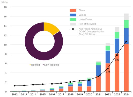
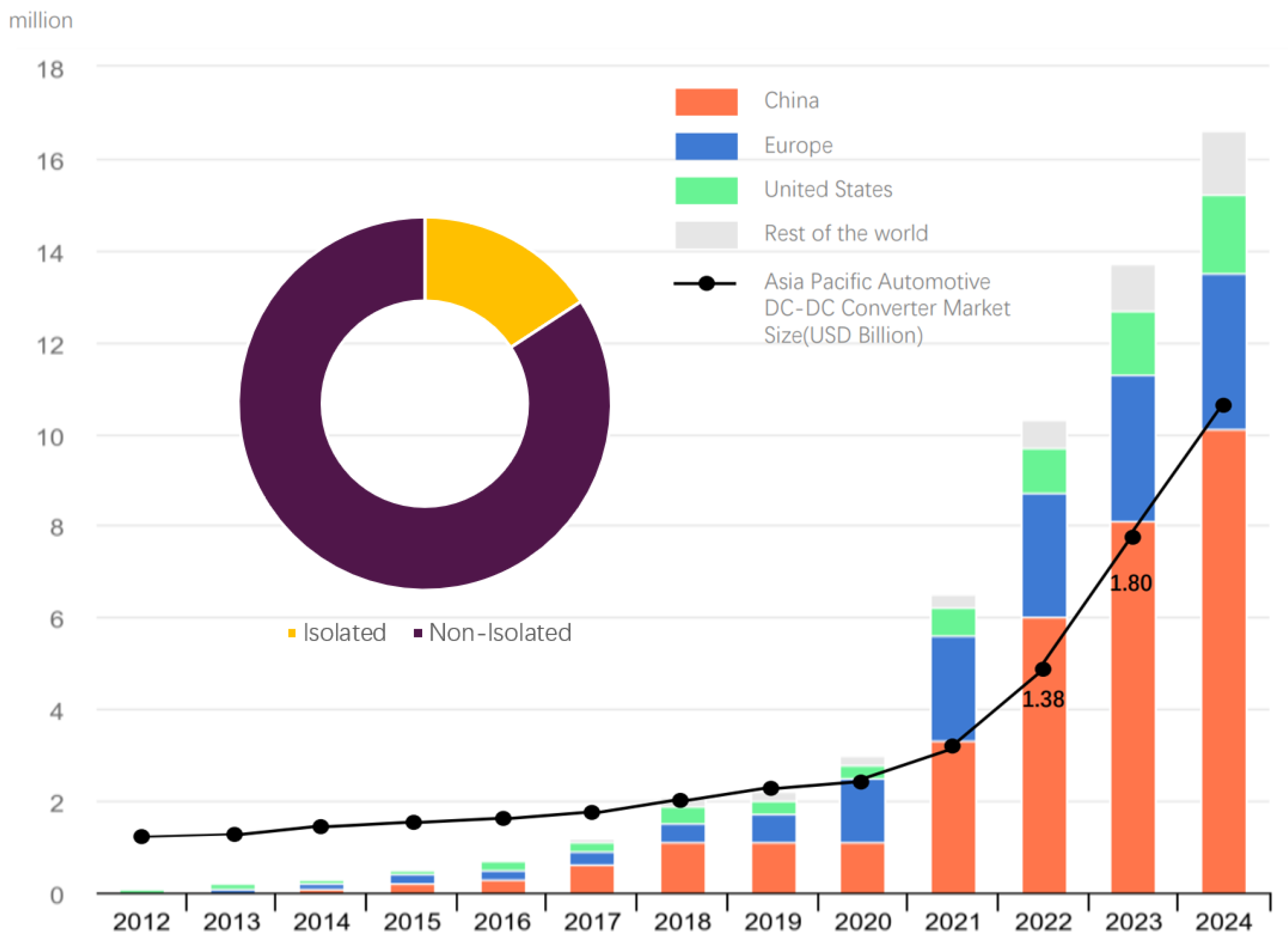
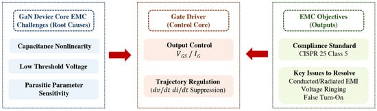
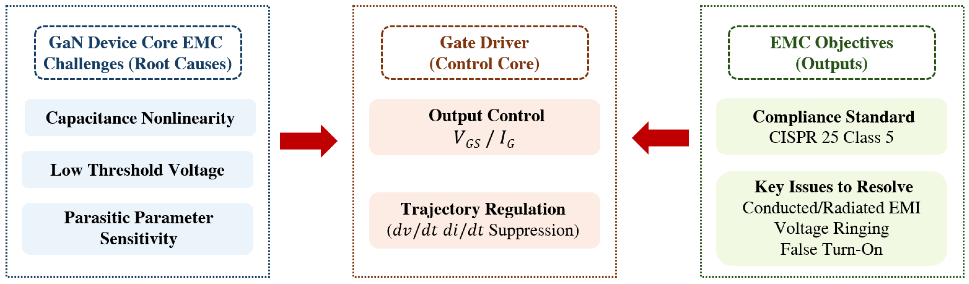
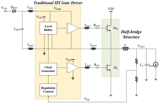
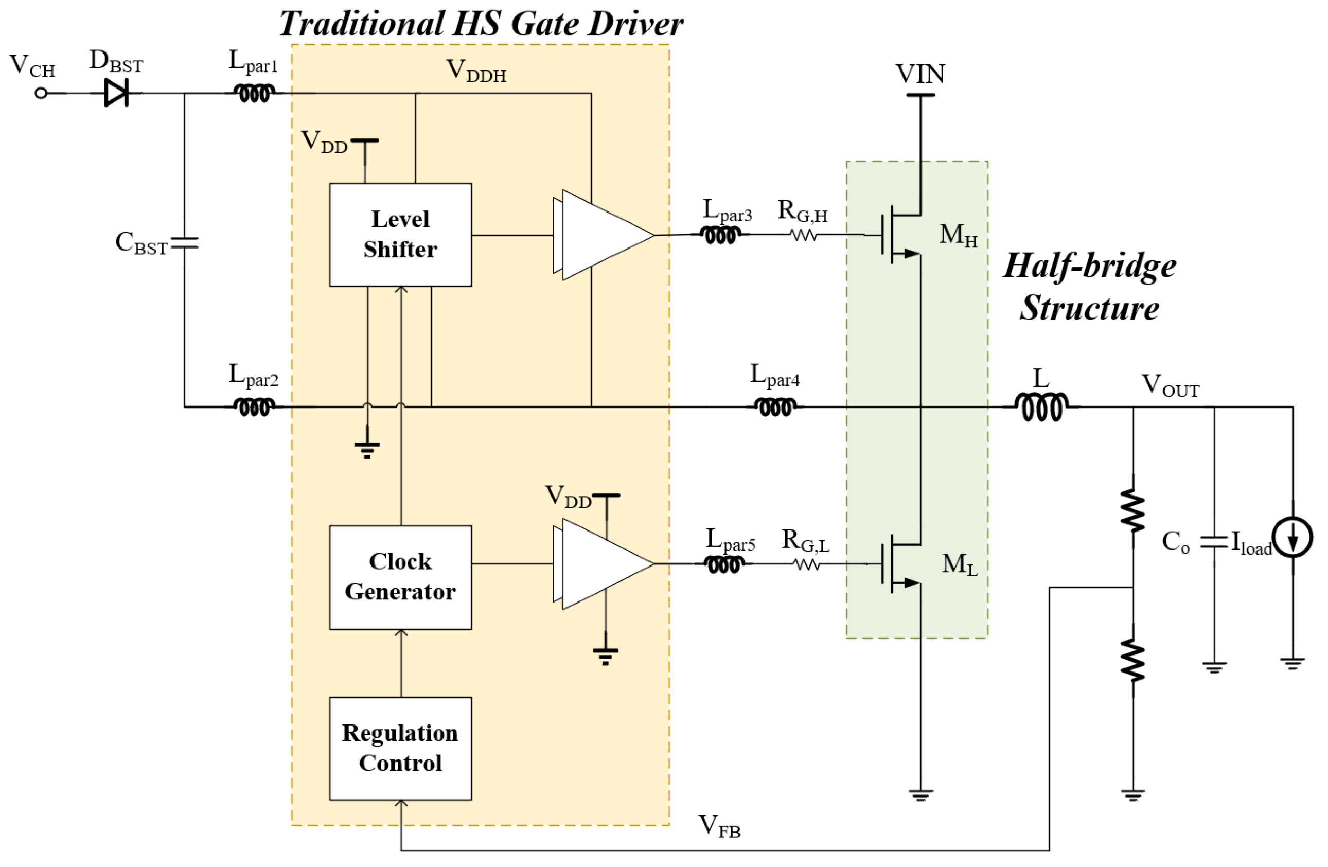
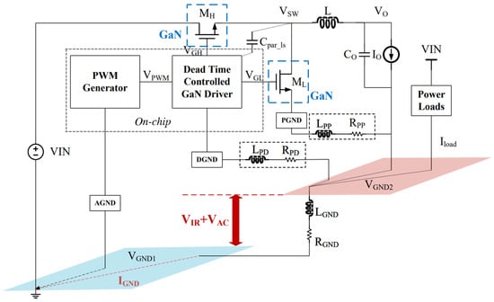
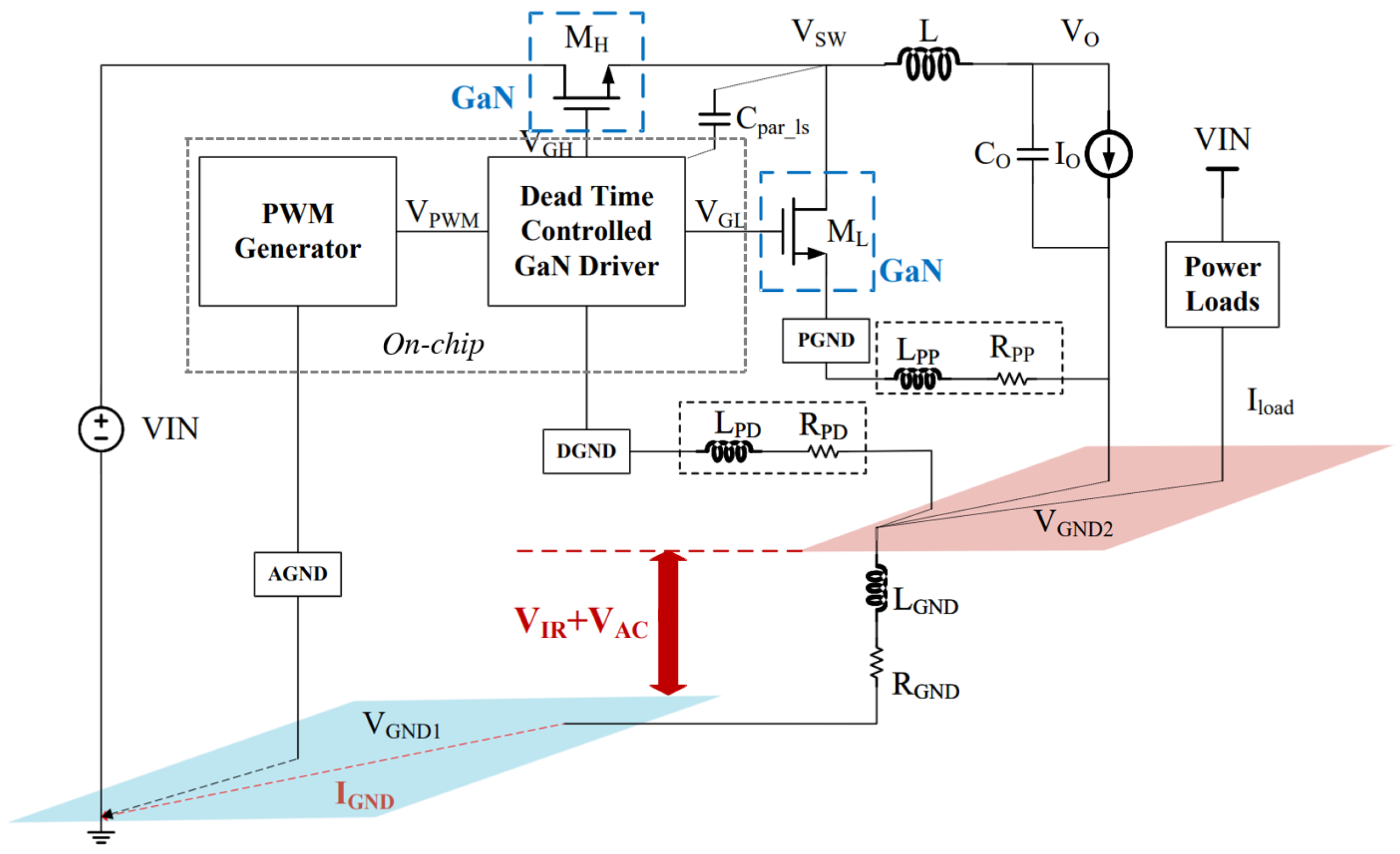
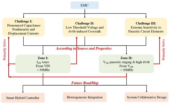
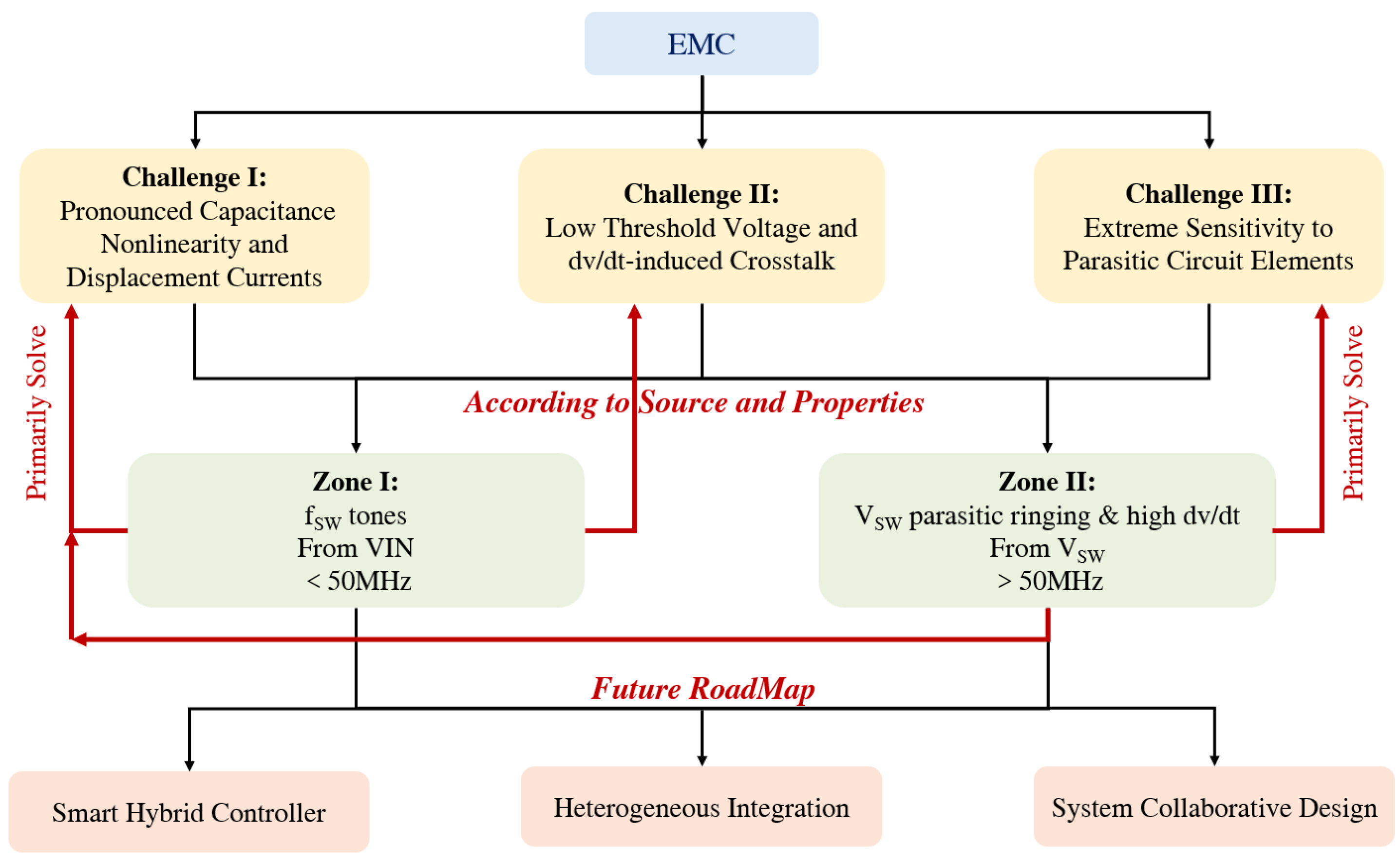
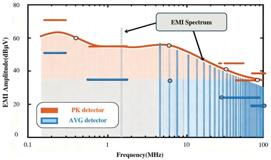
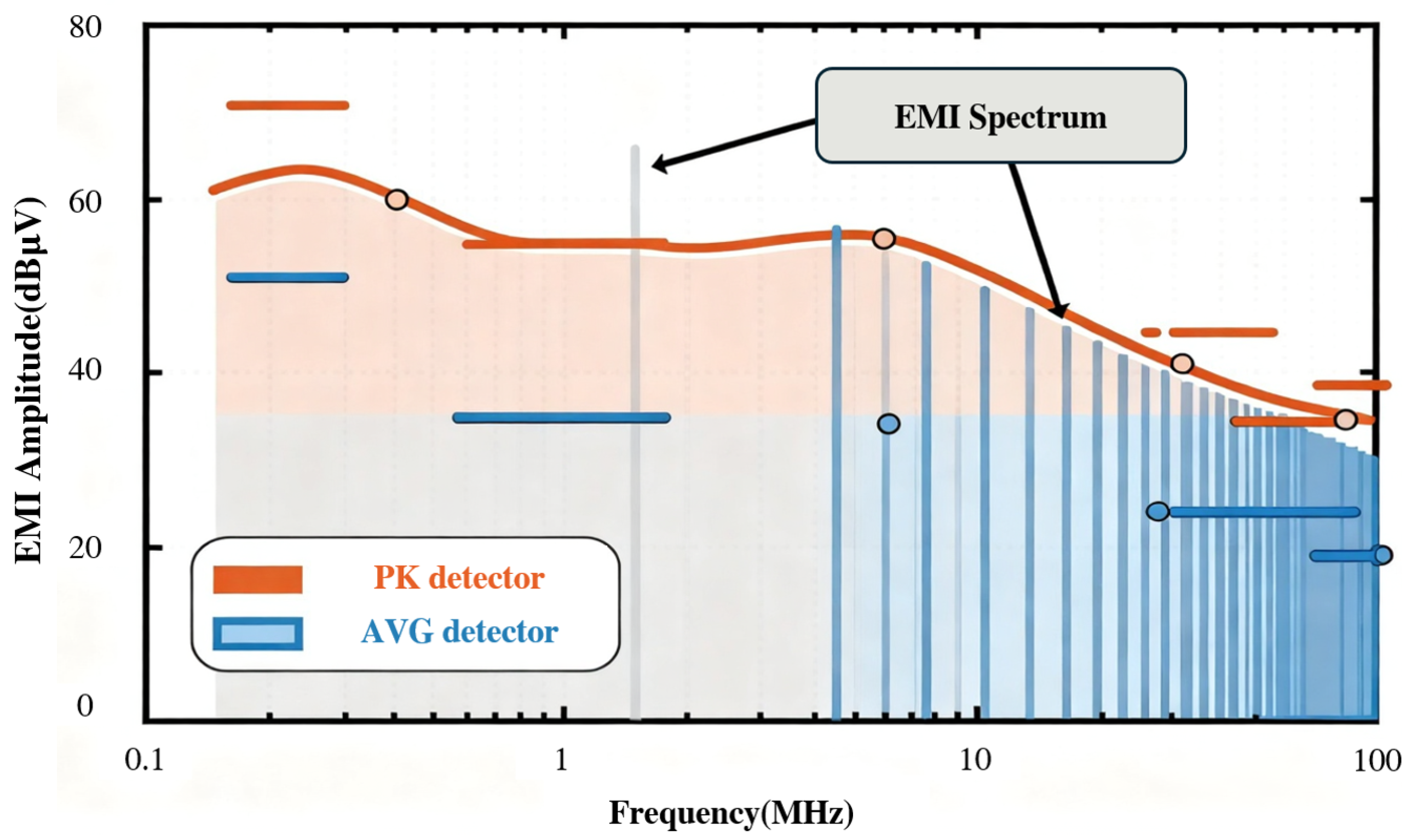
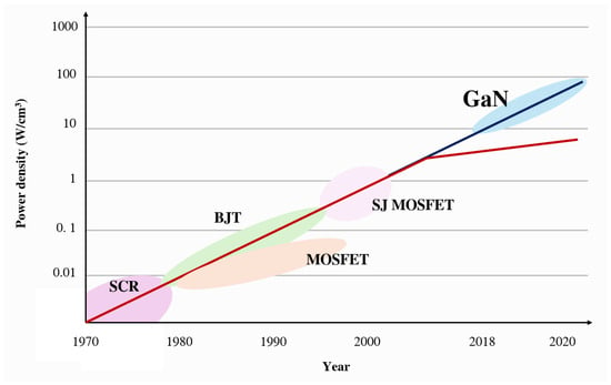
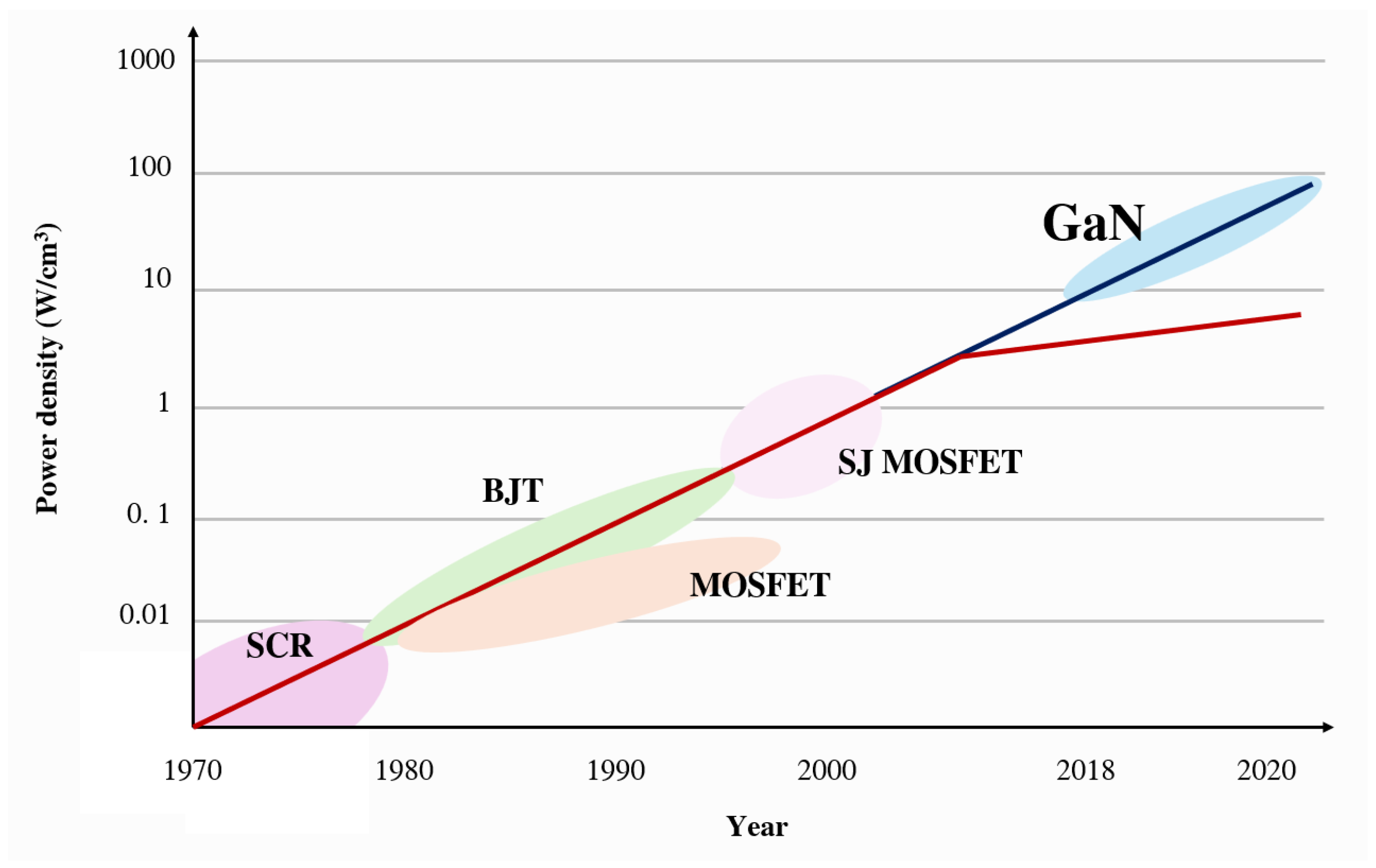
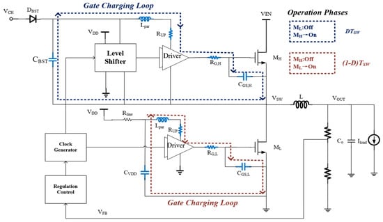
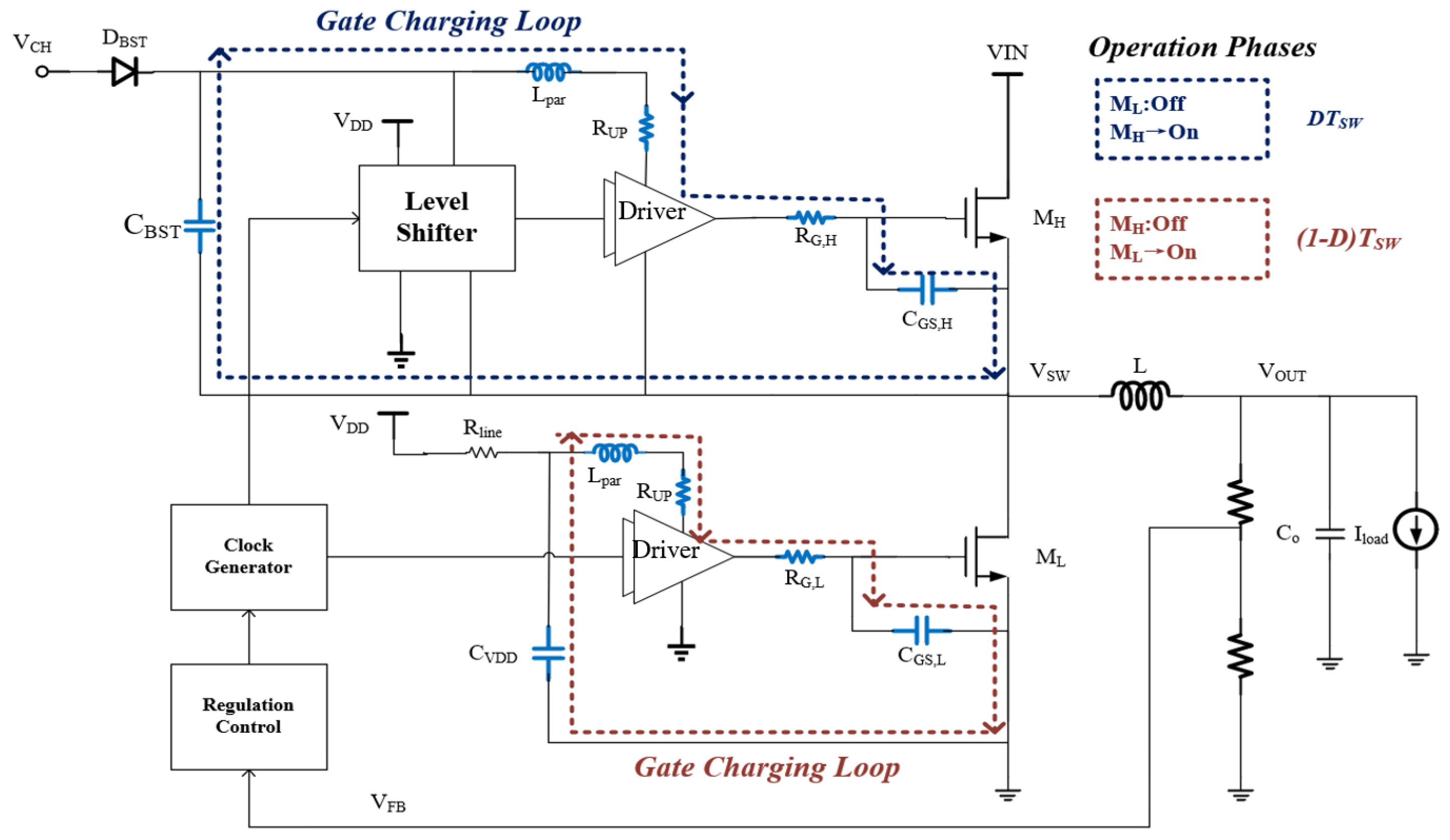
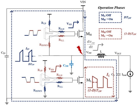
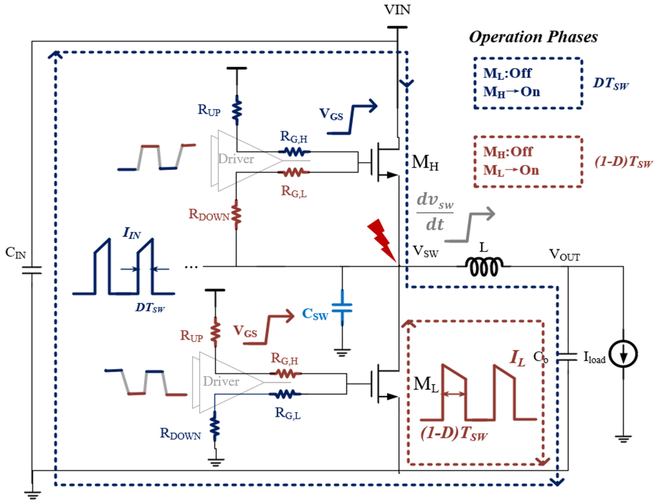
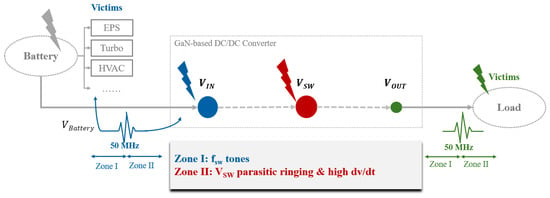
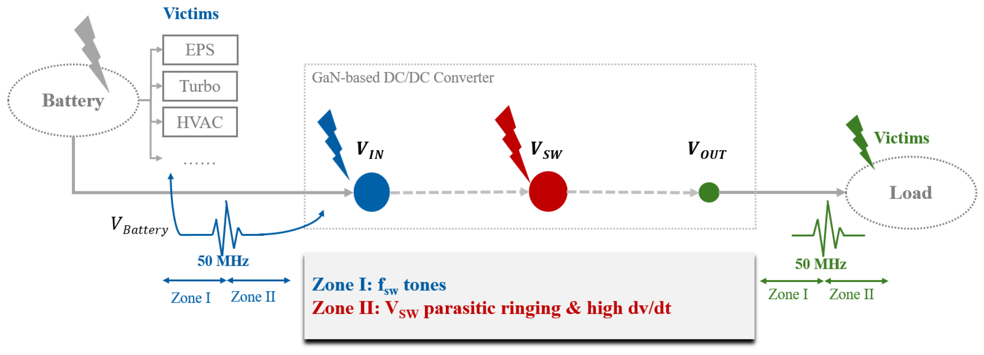
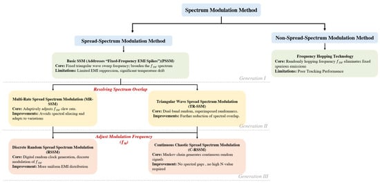
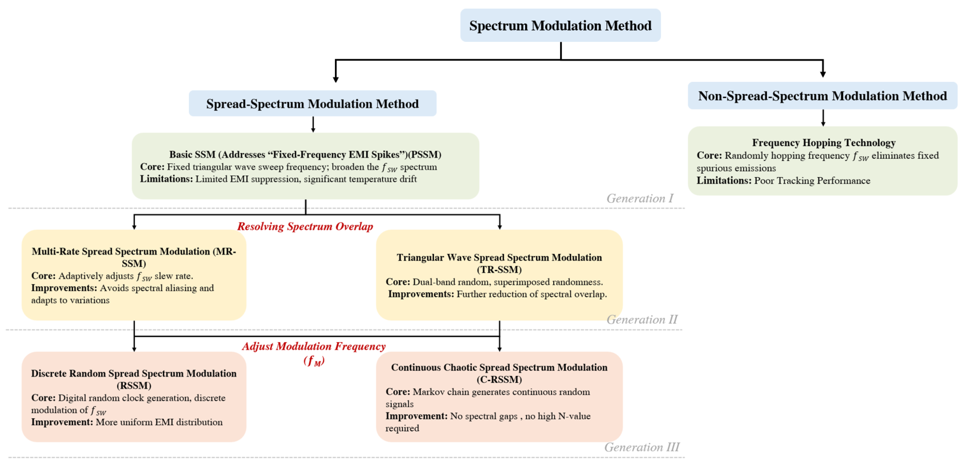
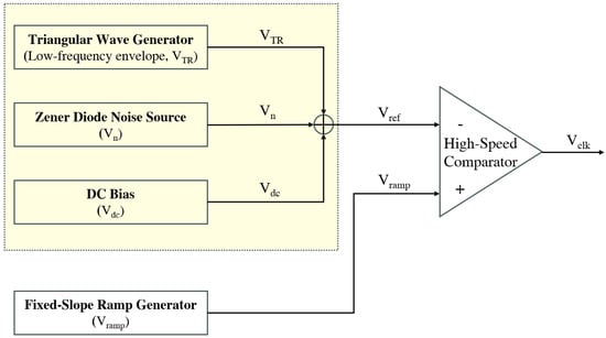
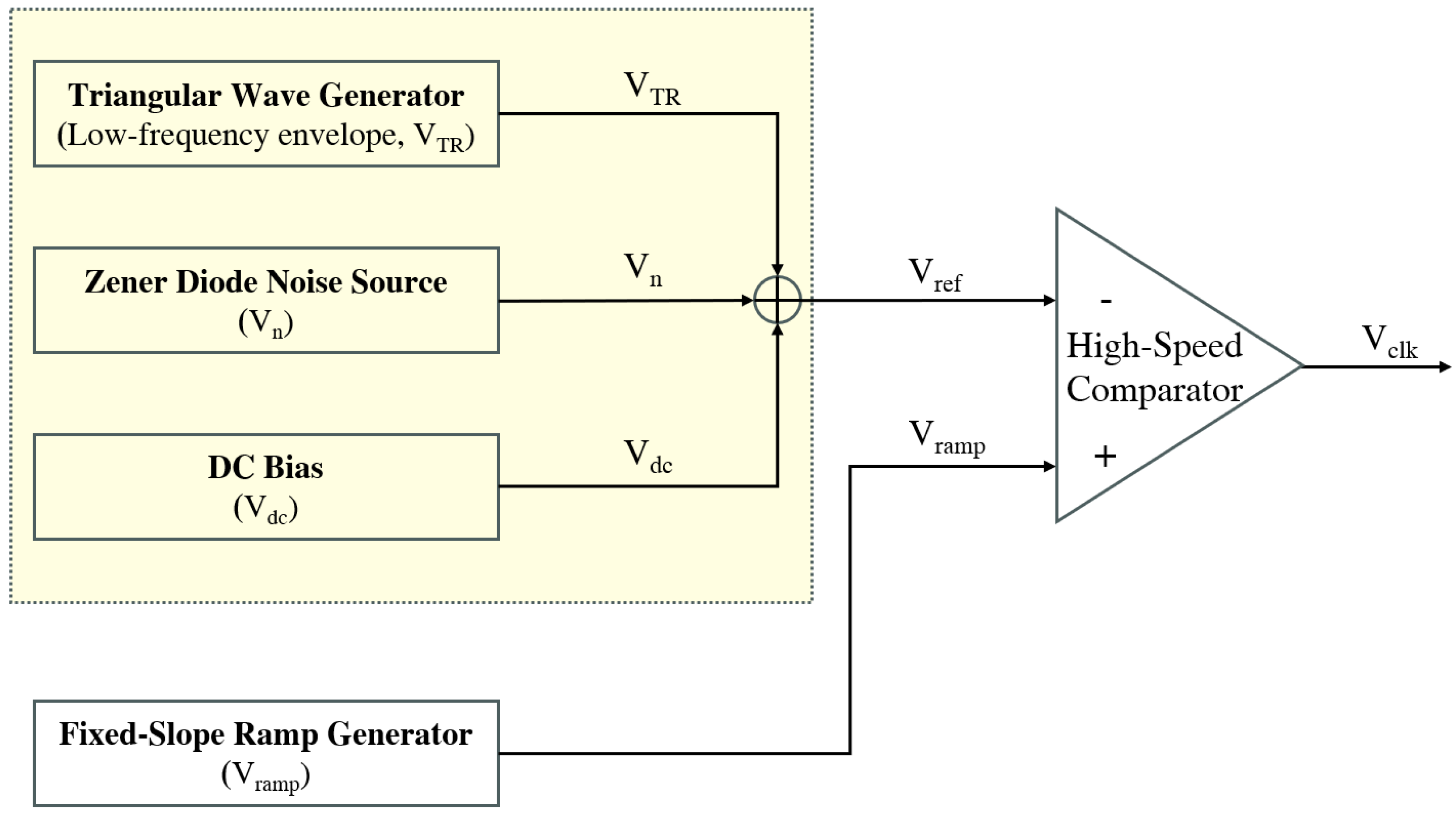
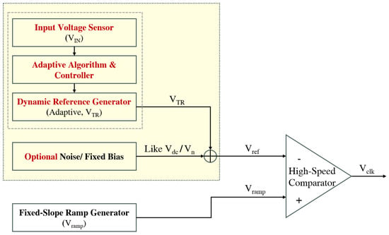
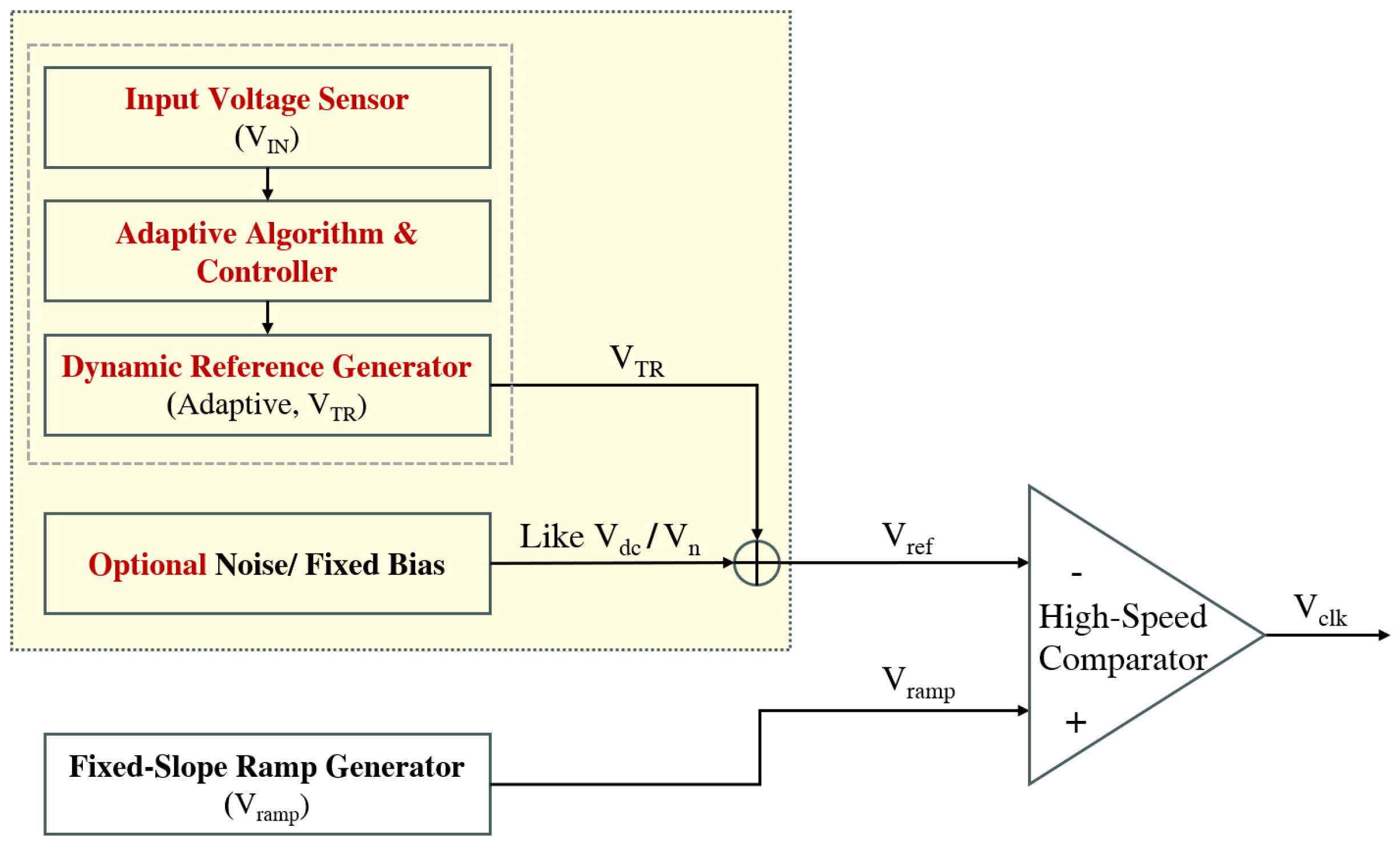
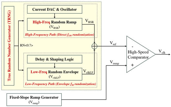
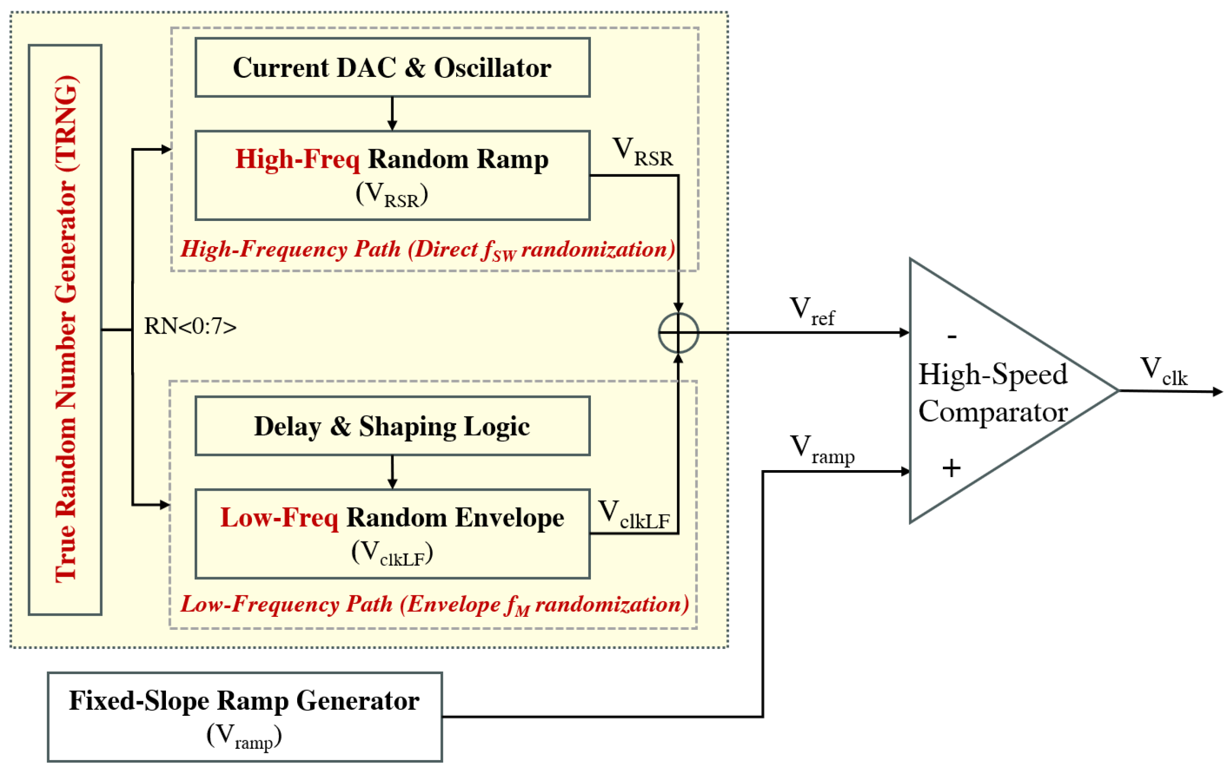
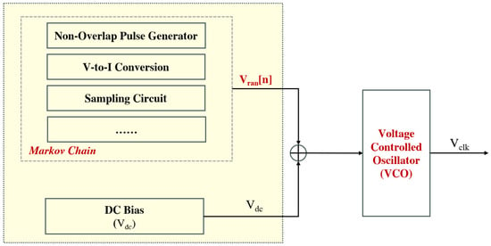
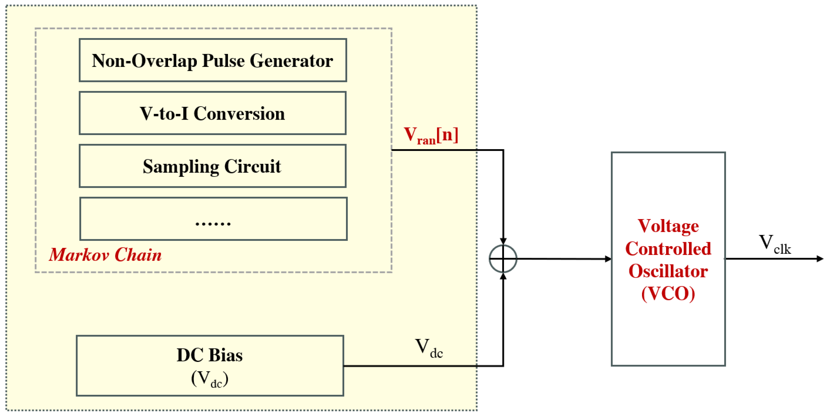
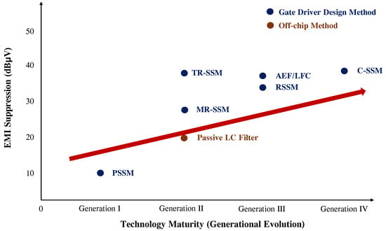
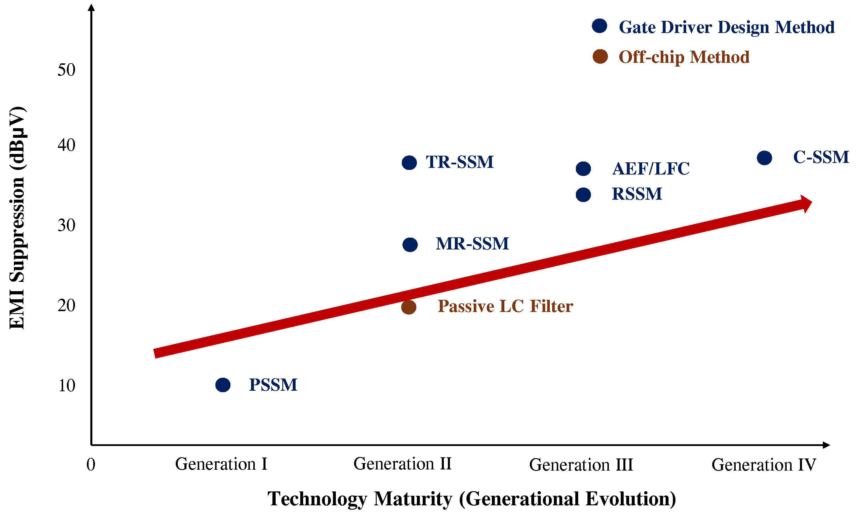
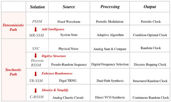
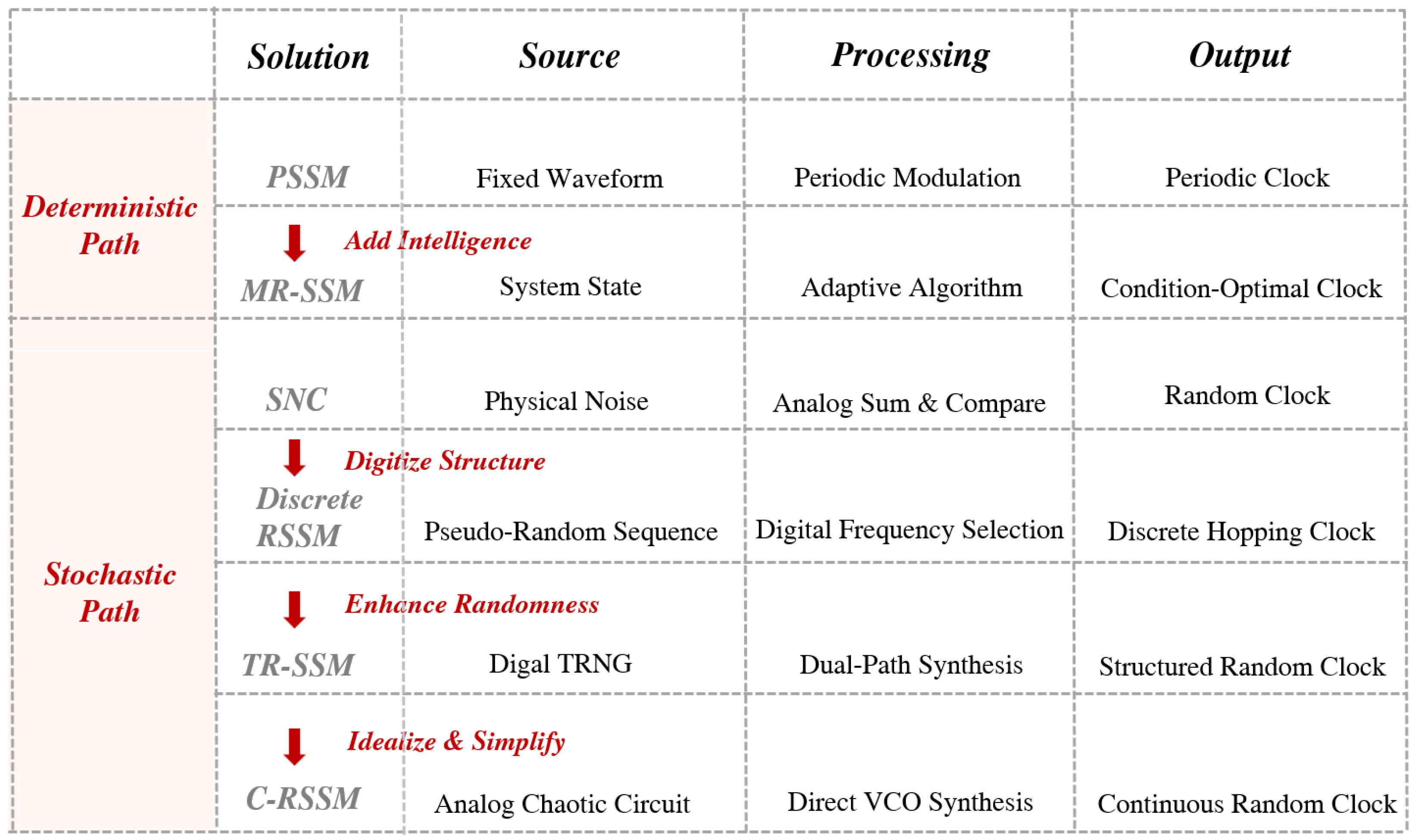
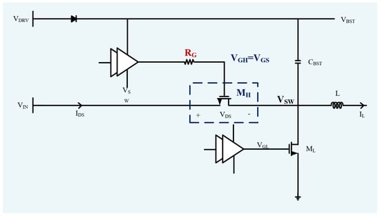
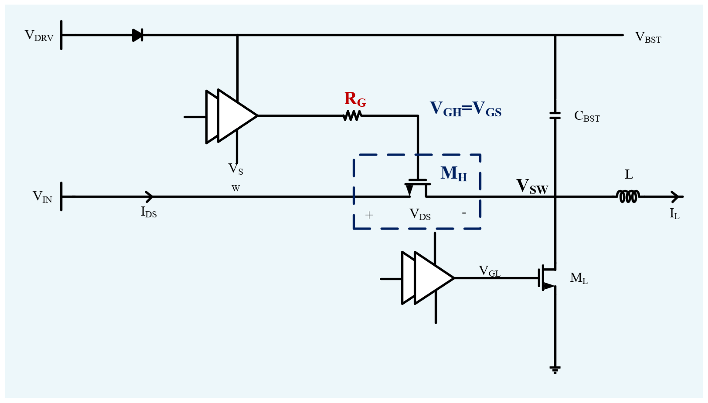
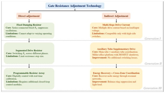
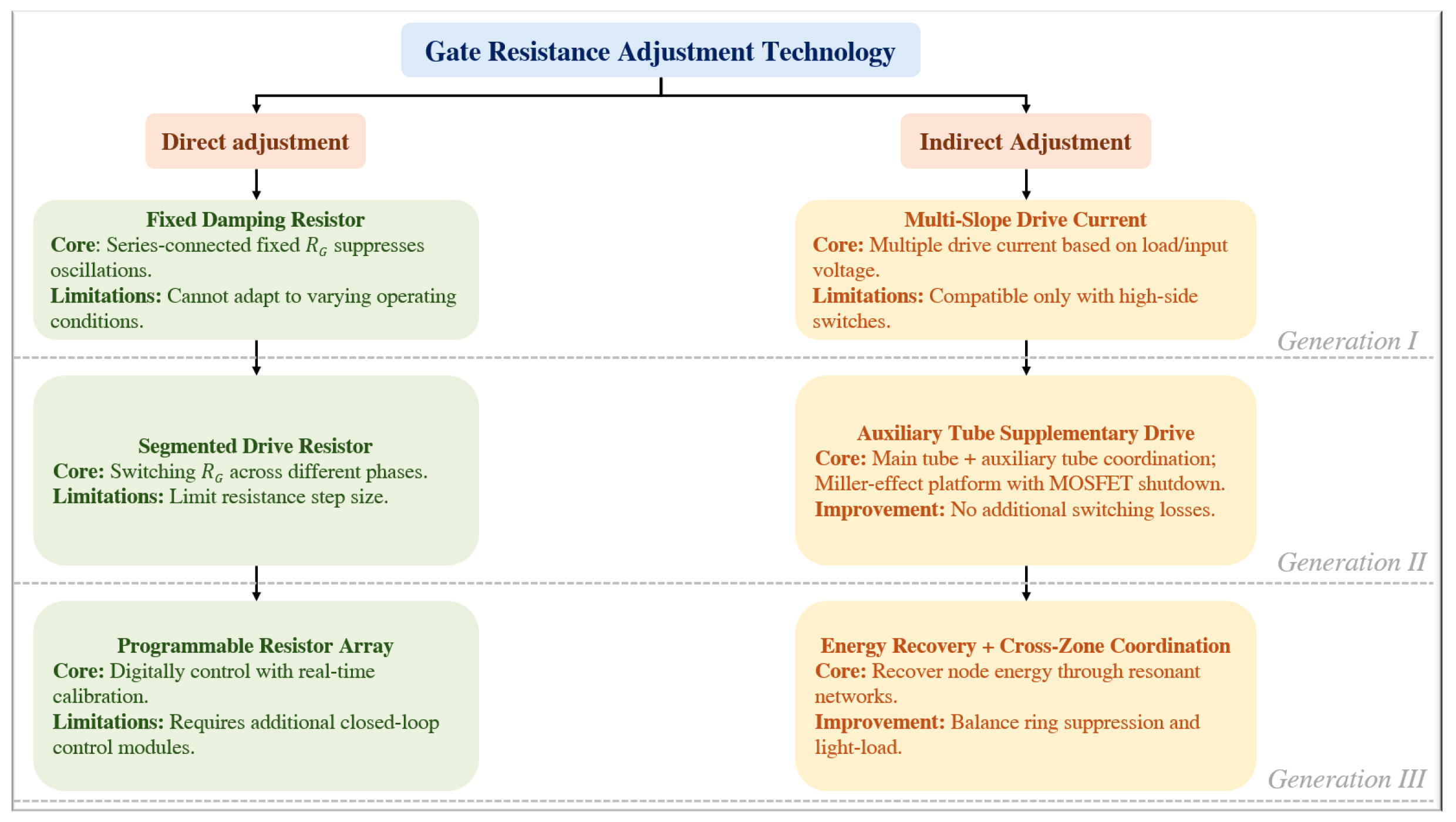
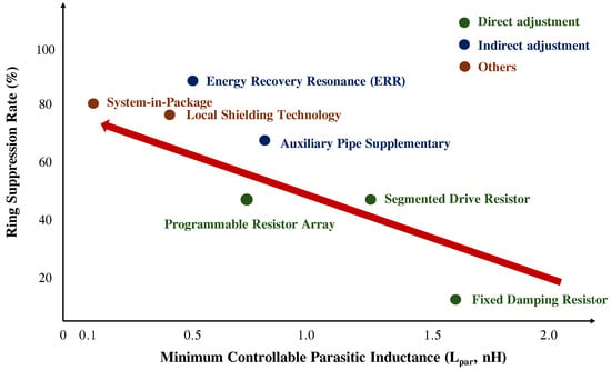
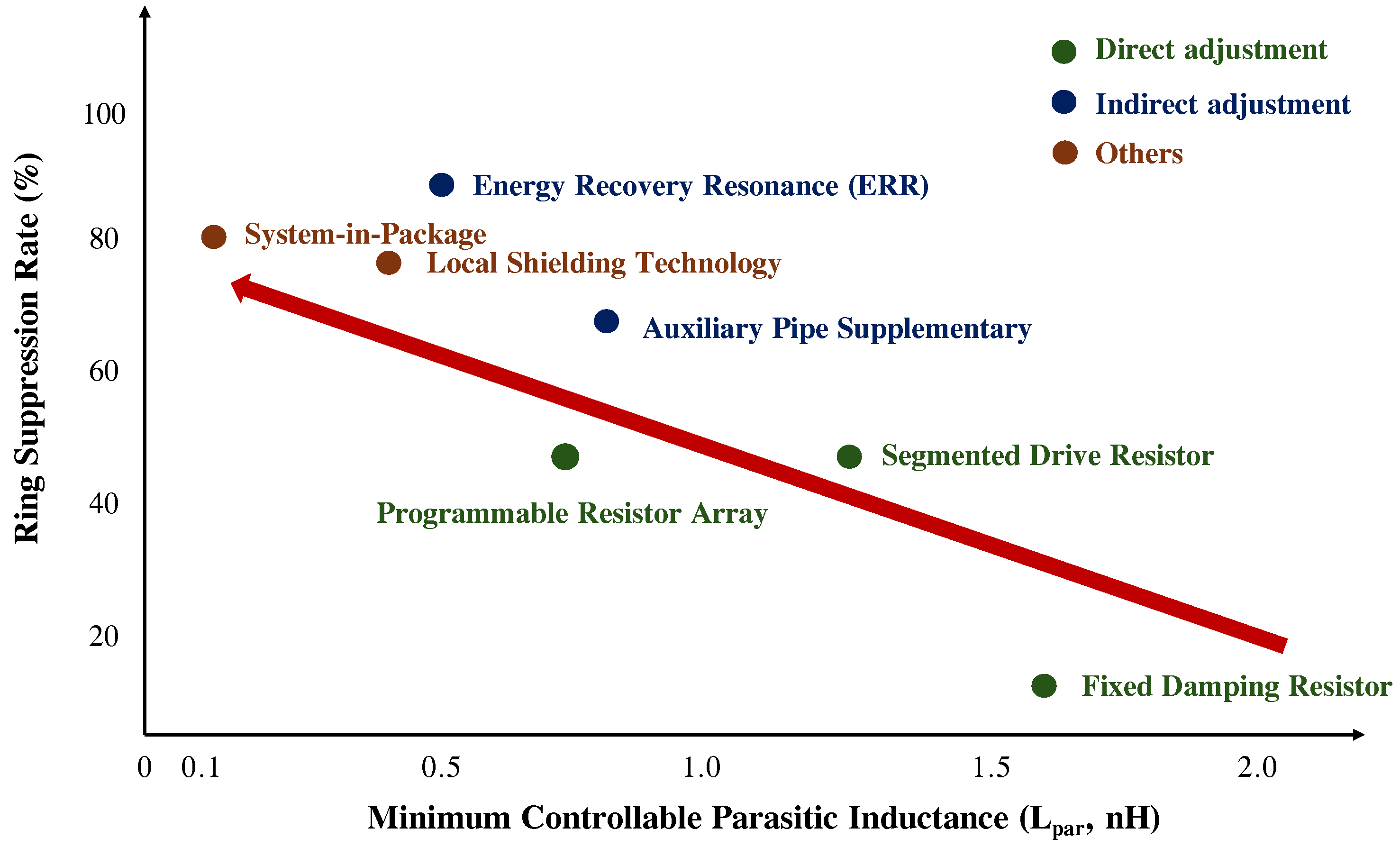
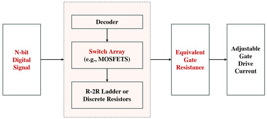
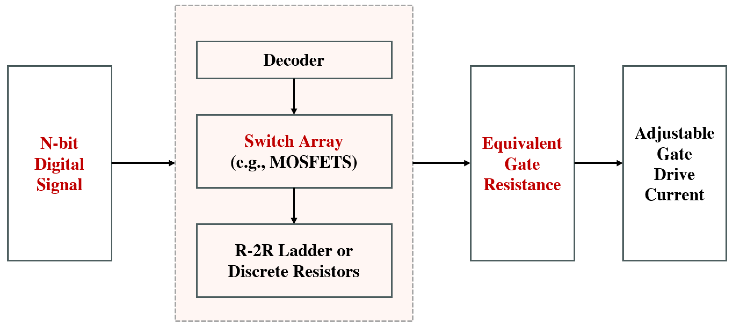
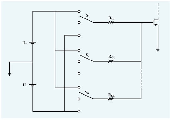
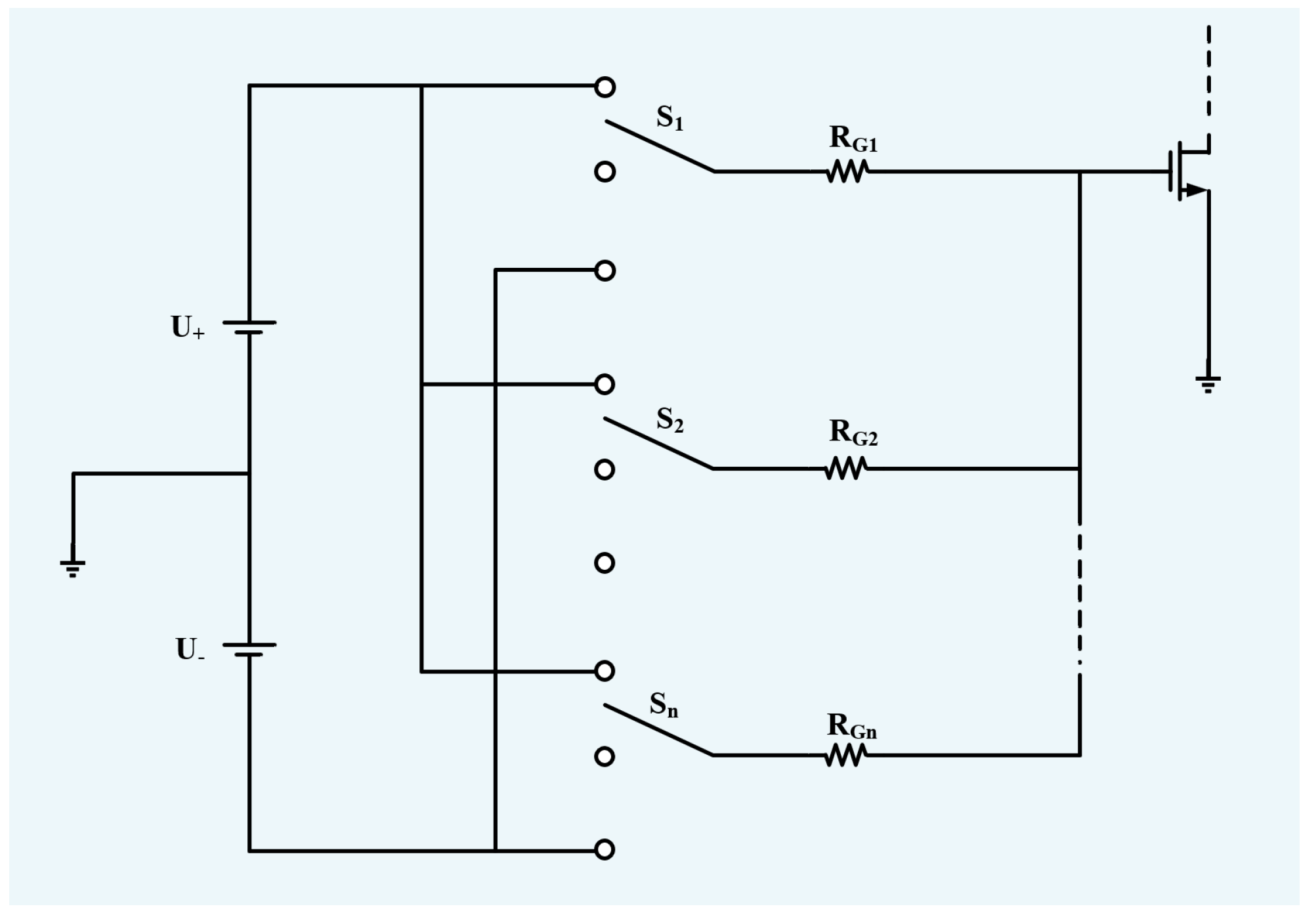
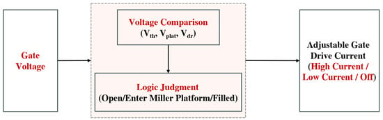
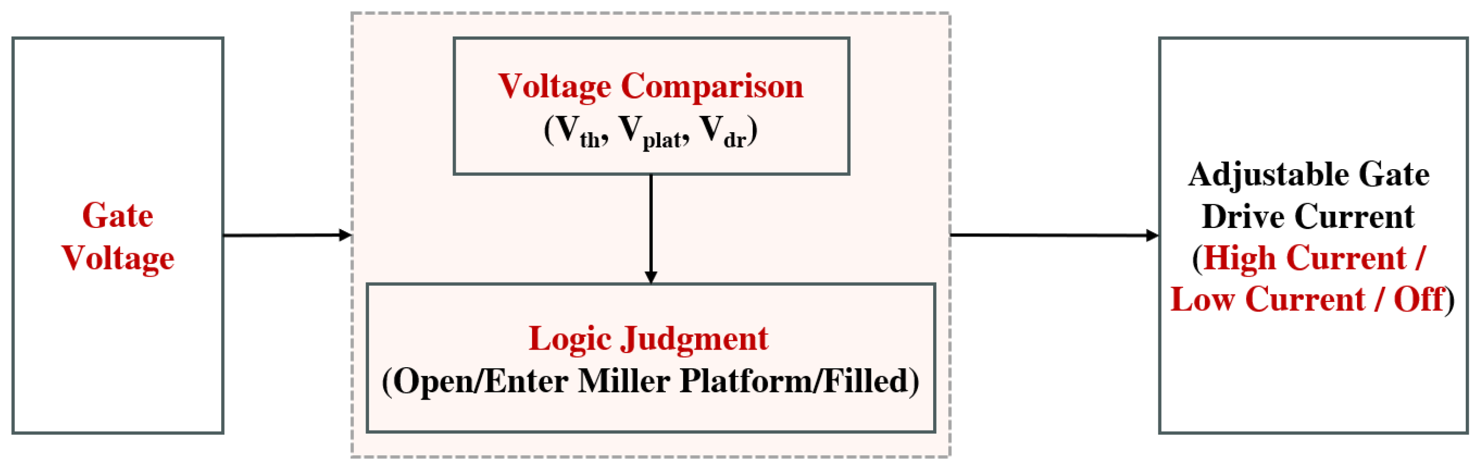
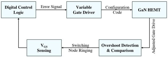
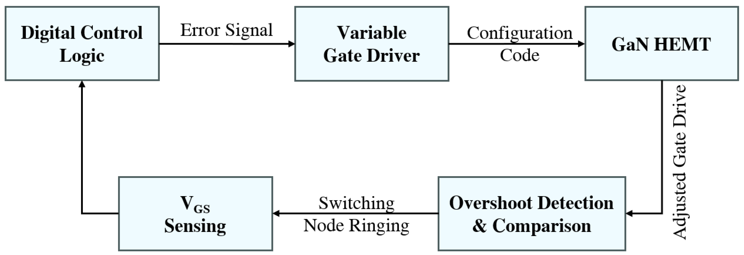
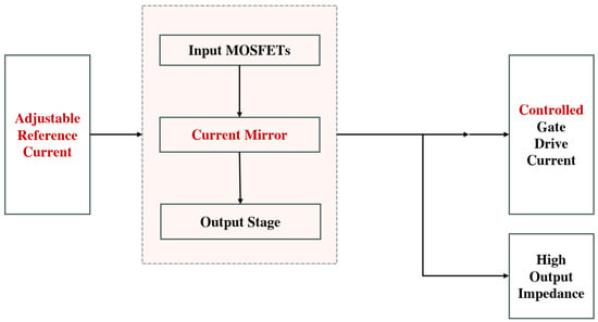
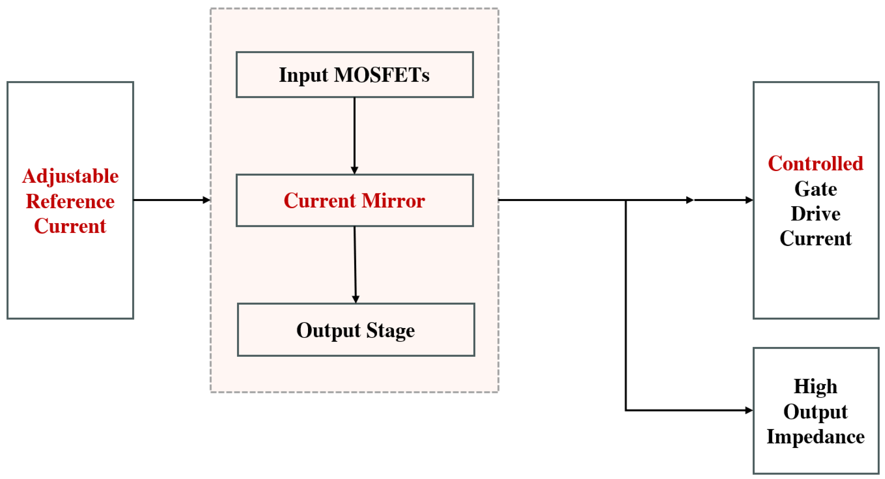
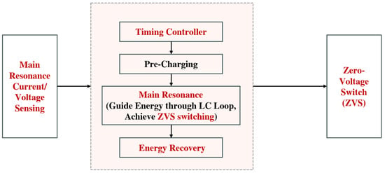
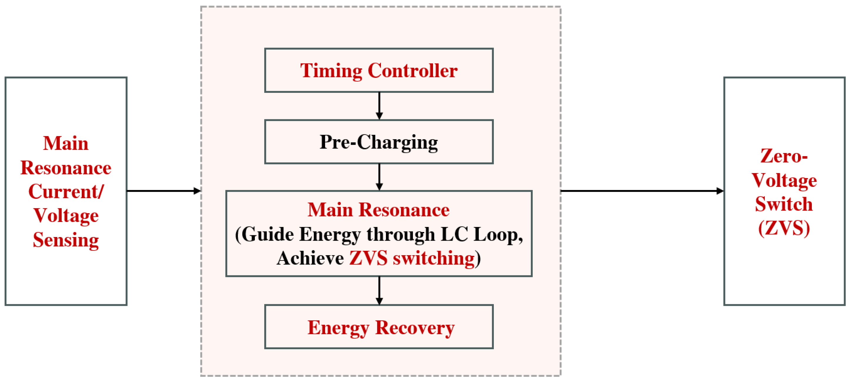
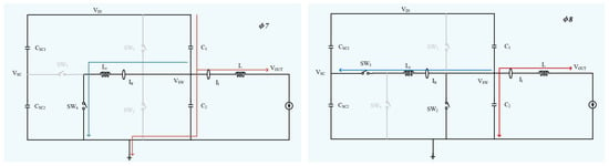
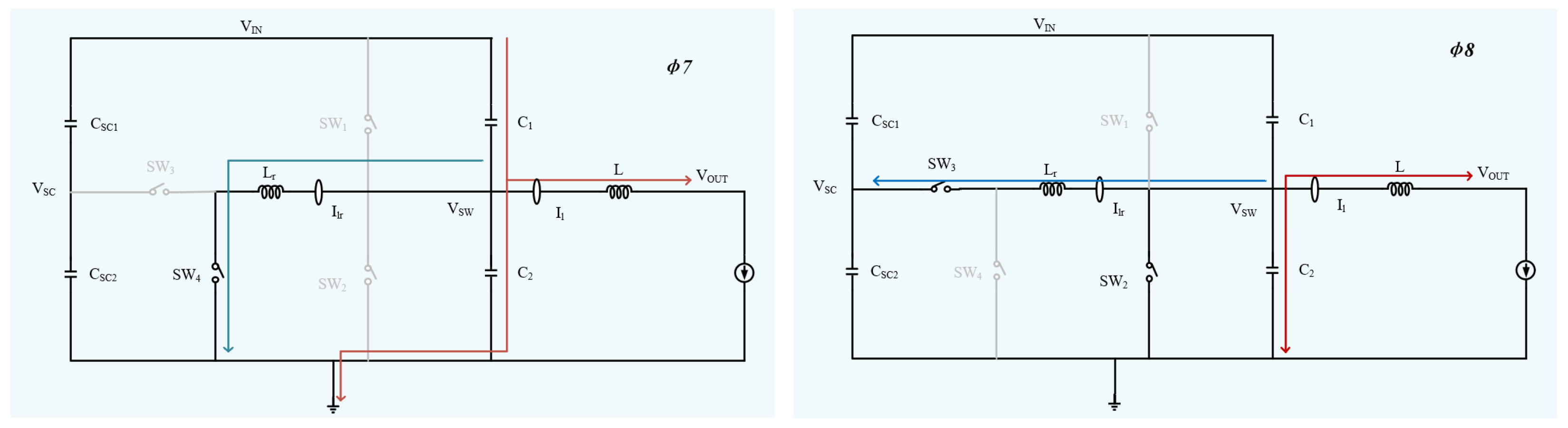
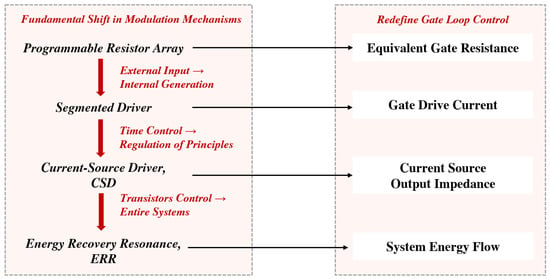
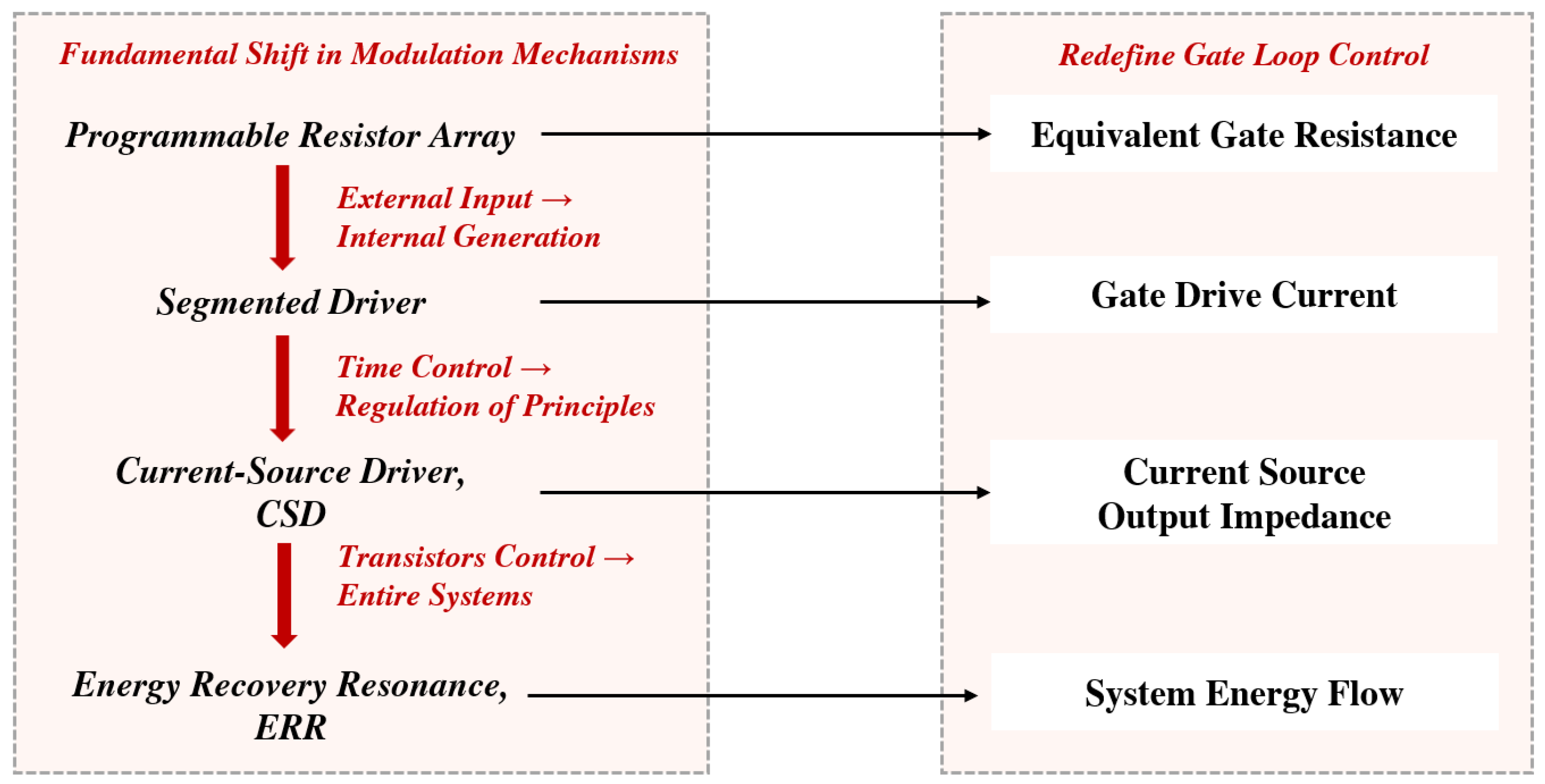
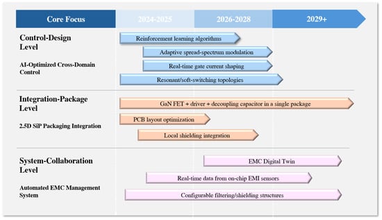
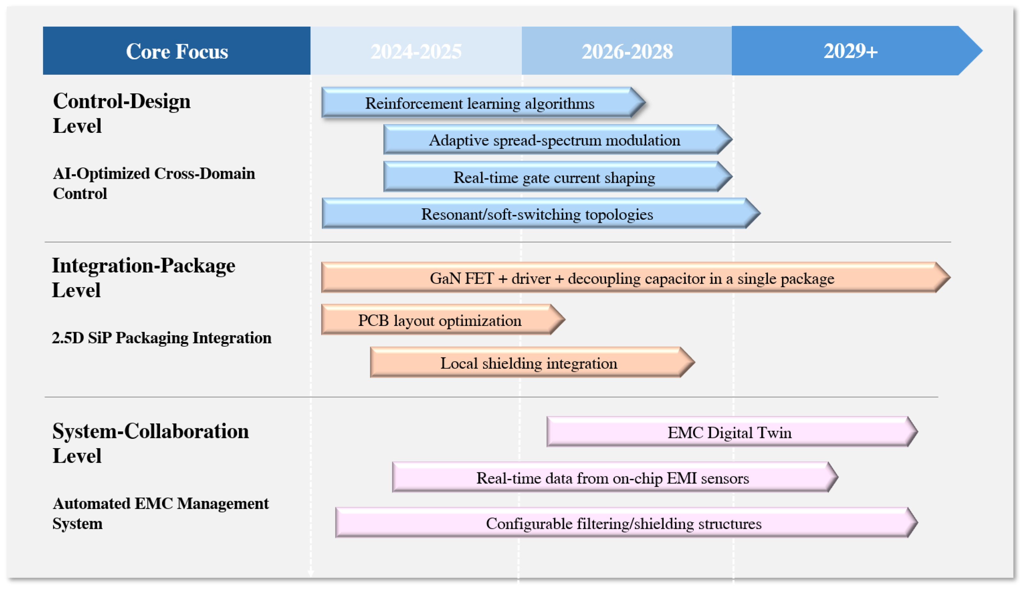

Disclaimer/Publisher’s Note: The statements, opinions and data contained in all publications are solely those of the individual author(s) and contributor(s) and not of MDPI and/or the editor(s). MDPI and/or the editor(s) disclaim responsibility for any injury to people or property resulting from any ideas, methods, instructions or products referred to in the content. |
© 2026 by the authors. Licensee MDPI, Basel, Switzerland. This article is an open access article distributed under the terms and conditions of the Creative Commons Attribution (CC BY) license.