


Abstract
In this article, we present a 60 GHz low-phase-error current-reuse variable-gain amplifier (VGA) in 65 nm CMOS. The proposed VGA consists of an input stage, a variable gain stage, and an output stage. An impedance-invariant VGA is used to reduce phase error during gain control. Furthermore, a transformer-based current-reuse technique is adopted to reduce dc power consumption and enhance the gain. Implemented in 65 nm CMOS technology, the proposed VGA occupies a chip area of 0.38 mm2, including pads, and consumes a dc power of 15 mW. The implemented design achieves a gain of 13.2 dB, a gain control range of 20 dB, and an RMS phase error less than 2.65° over 50–67 GHz. Additionally, the input 1-dB compression point is −11 dBm at 60 GHz.
1. Introduction
In recent years, the 60 GHz millimeter-wave (mm-wave) spectrum has garnered significant attention for enabling low-latency applications, short-range radar systems, and ultra-fast wireless networks [1,2,3,4,5,6]. Nevertheless, standard CMOS-based single-chip transceivers face fundamental constraints regarding output power, a problem that is further compounded by the substantial free-space path loss inherent to mm-wave propagation. To extend the operational range and enhance link reliability, modern communication frameworks, including emerging 6G networks and IEEE 802.11ad/ay standards, rely heavily on phased-array beamforming architectures to drastically boost the effective isotropic radiated power (EIRP) [7,8].
While phased-array systems offer numerous structural benefits, they are naturally prone to pronounced sidelobe emissions, which generate severe spatial interference and diminish overall antenna directivity. Amplitude tapering across the array elements is a widely utilized and effective strategy to suppress these undesired sidelobes [8,9]. Consequently, implementing variable-gain amplifiers (VGAs) capable of broad gain adjustment has become essential for executing accurate beam-tapering within modern phased-array transceivers [8,9].
For precise beam-tapering applications, it is critical that the VGA maintains a constant insertion phase regardless of the selected gain state. Any phase fluctuation during amplitude control leads to substantial beam-pointing inaccuracies, which completely cancel out the benefits of sidelobe suppression. To tackle this challenge in CMOS processes, several impedance-invariant VGA (IIVGA) topologies [10,11,12,13] have been introduced. These architectures typically preserve consistent input and output impedances by balancing the on- and off-state transistors at each node. However, existing IIVGA designs face noticeable limitations. For instance, analog control methods [10] suffer from degraded phase invariance due to parasitic capacitance and biasing variations. Single-stack architectures [11] often exhibit a restricted gain-tuning range or lack adequate dB-linear control, whereas triple-stacked topologies [12,13] inevitably require undesirably high supply voltages. Other implementations [14], such as current-steering cascode designs with impedance compensation, suffer from limited 1-dB compression points. Although shunt common-source/common-gate (CS-CG) configurations have been explored [15], their gain control ranges remain heavily constrained. Therefore, realizing a CMOS VGA that simultaneously guarantees strict phase invariance, wide gain control, and high linearity under stringent power and voltage limitations remains a prominent design challenge.
To overcome these existing hurdles, this paper presents a 60 GHz high-gain, low-phase-variation VGA implemented in 65 nm CMOS technology. To ensure minimal phase shift during gain tuning, we propose an advanced impedance-invariant structure that structurally locks the insertion phase across all operating states. Moreover, an efficient current-reuse technique is incorporated to enhance the gain without additional dc power consumption, making the proposed architecture highly suitable for power-constrained mm-wave phased-array networks.
2. Design Methodology
2.1. Design Considerations
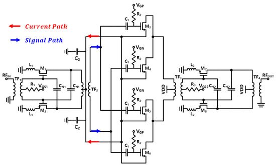
Figure 1 illustrates the schematic of the proposed 60 GHz VGA for a beam-forming transceiver. The architecture consists of three main blocks: an input stage, an impedance-invariant variable-gain (IIVG) stage, and an output stage. In 65 nm CMOS technology, designing at 60 GHz poses inherent challenges, such as a low intrinsic gain and significant parasitic capacitances that severely degrade both stability and gain. Furthermore, conductive substrate losses typically limit the efficiency of passive components. To overcome these limitations, we utilized the thick top metal layers provided by the 65 nm process to implement high-Q transformers and inductors, minimizing losses. Additionally, rather than cascading multiple stages to compensate for the low intrinsic gain, we adopted a transformer-based current-reuse technique combined with an impedance-invariant current-steering structure. These design choices prevent the gain degradation commonly found in traditional phase-invariant VGAs. Consequently, the proposed architecture enhances gain, stability, and power efficiency within a limited power budget while maintaining a constant insertion phase during gain tuning.
Figure 1.
Schematic of proposed VGA.
2.2. Input and Output Stages
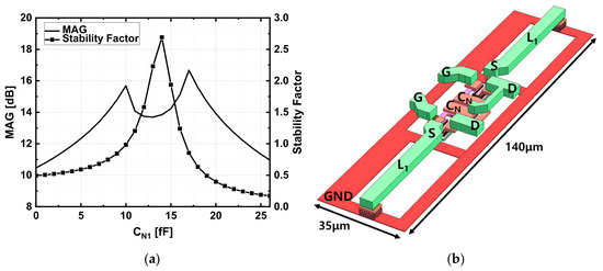
Both the input and output stages employ differential common-source topologies. At mm-wave frequencies such as 60 GHz, the intrinsic gate-drain parasitic capacitance, Cgd, of the transistors severely degrades the reverse isolation and potential stability of the amplifier. To ensure unconditional stability and improve the maximum available gain (MAG), cross-coupled neutralization capacitors, CN1 and CN2, are integrated across the gate-drain terminals of the differential pairs, M1, M2, and M7, M8 [16,17]. Figure 2a illustrates the simulated MAG and stability factor (K) of the common-source amplifier as a function of the neutralization capacitance. By optimally sizing CN1, the stability factor is securely maintained above 1 for unconditional stability, while the MAG is enhanced. In this design, transistors M1, M2, M7, and M8, with a width of 2 μm and 25 fingers, are selected, and both of the neutralization capacitors, CN1 and CN2, are chosen to be 13.5 fF for better power gain, isolation, and stability. With the neutralization technique, the input and output stages achieve a MAG of 13.8 dB, an improvement of 3.3 dB compared to the design without a neutralization capacitor, CN1.
Figure 2.
Input and output stages: (a) Simulated MAG and stability factor of the common-source amplifier with neutralization capacitor CN, and (b) Layout of amplifier core with neutralization capacitors and inductor L1.
To precisely implement these sensitive neutralization capacitors, a custom-designed metal-oxide-metal (MOM) capacitor is utilized rather than a standard foundry-provided component [16]. As depicted in the 3-D layout of the amplifier core in Figure 2b, the custom MOM capacitor employs a multi-stack metal plate design. This customized structure allows for a highly compact chip area and significantly shorter interconnections, while utilizing sufficient vias to dramatically reduce parasitic resistance. Furthermore, simulations demonstrate that the custom MOM capacitor exhibits a minimal process variation of less than ±2%, a substantial improvement over the ±11% variation typical of standard foundry MOM capacitors. This extremely low variation is crucial for maintaining accurate cross-coupling balance and robust neutralization performance across PVT corners.
In addition to the custom capacitors, source degeneration inductors L1 and L2 are strategically inserted at the source nodes of the differential amplifying transistors. The addition of these source inductors introduces series negative feedback, which significantly enhances the overall linearity of the amplifier and provides an additional margin for stability without severely penalizing the gain or noise performance.
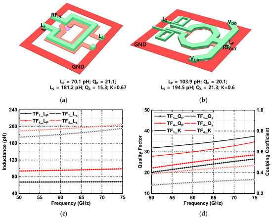
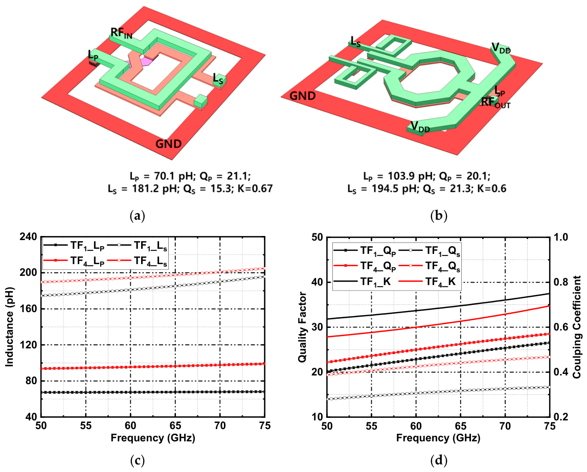
A highly efficient matching network is crucial for maximizing the overall gain and maintaining wideband performance in millimeter-wave circuits. Figure 3 illustrates the 3-D EM layouts, inductances, quality factors (Q-factors), and coupling coefficients (k-factors) of the input and output transformer-based baluns TF1 and TF4, which are implemented using the thick top metal layers to minimize resistive losses and achieve high quality factors.
Figure 3.
3-D layouts of (a) input transformer TF1 and (b) output transformer TF4, and simulated (c) inductances and (d) quality factors and coupling coefficients of TF1 and TF4.
The input transformer TF1, shown in Figure 3a, acts as a single-ended-to-differential balun and provides upward impedance transformation to boost the voltage swing at the gate of the input stage. The simulated primary and secondary inductances are 70.1 pH and 181.2 pH, respectively, with a k-factor of 0.67 as shown in Figure 3c,d. The corresponding peak Q-factors at 60 GHz are 21.1 and 15.3, demonstrating excellent passive efficiency.
Similarly, the output transformer TF4, depicted in Figure 3b, converts the differential signal back to single-ended for measurement and system integration. The primary and secondary inductances are 103.9 pH and 194.5 pH, respectively, with a k-factor of 0.6. Since the insertion loss of a transformer is heavily dependent on its k-factor, selecting the appropriate k value is essential. While a higher k-factor reduces insertion loss, a moderately lower k-factor helps expand the bandwidth. Therefore, a k value of 0.6 was carefully optimized to achieve the best trade-off between wideband matching and low insertion loss across the 50–67 GHz band.
To accurately isolate substrate noise and define signal return paths, a ground plane with a mesh pattern utilizing the bottom metal layers is placed beneath the transformers. All passive components in this design, including the transformers, source degeneration inductors, custom MOM neutralization capacitors, and interconnections, were rigorously designed and verified using the HFSS 2025 3-D EM simulator developed by Ansys, Canonsburg, PA, USA, to capture accurate high-frequency parasitic effects.
2.3. Transformer-Based Current-Reuse Topology
To minimize the total dc power consumption without sacrificing the forward gain, a transformer-based current-reuse technique is adopted between the input stage and the variable gain stage. As illustrated in Figure 1, the two stages share the same dc bias current. The dc current originates from the VDD supply connected to the center tap of the primary inductor of TF3, flows through the variable gain stage transistors, M3–M6, and exits from their common-source nodes. Instead of being routed to ground, this dc current is directly injected into the center tap of the primary inductor of TF2, thereby serving as the supply current for the input stage. At this dc current path, a bypass capacitor, C2, is connected to the center tap of TF2 to establish an ac ground. This ensures that the common-source nodes of M3–M6 are effectively grounded at RF frequencies, allowing them to operate as common-source amplifiers. Simultaneously, the RF signal is magnetically coupled from the primary to the secondary inductor of TF2 and fed into the variable-gain stage through dc-blocking capacitors, C1. This transformer-coupling structure perfectly isolates the dc bias domains of the stacked stages while providing wideband ac impedance matching, leading to high gain with significantly reduced power dissipation.
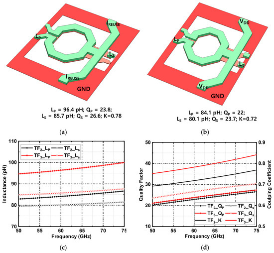
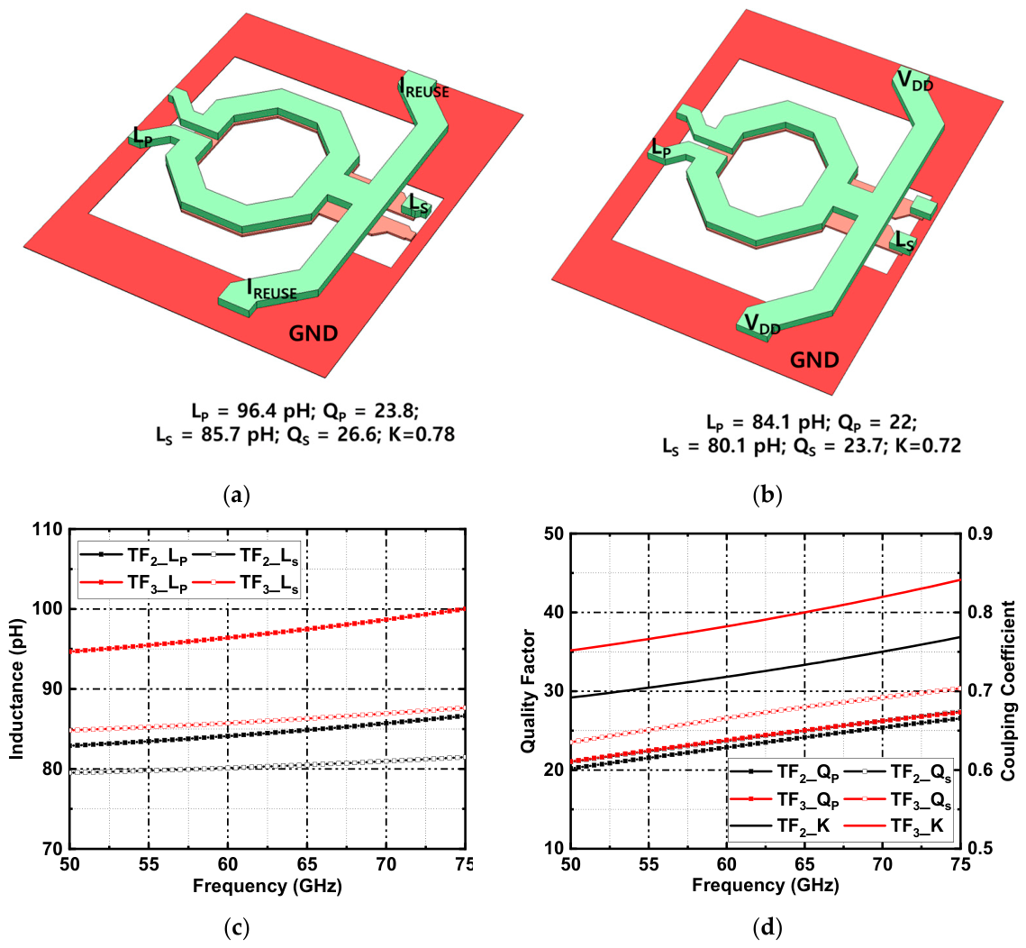
Similar to the input and output baluns, highly efficient inter-stage matching transformers TF2 and TF3 are strictly required to transfer the RF signal between the stages while enabling the proposed current-reuse topology. Figure 4 illustrates the 3-D EM layouts, inductances, Q-factors, and k-factors of the inter-stage matching transformers. Both TF2 and TF3 are implemented using the thick top metal layers over a mesh ground plane to minimize substrate loss and ensure high quality factors.
Figure 4.
3-D layouts of inter-stage matching transformers, (a) TF2 and (b) TF3, and simulated (c) inductances and (d) quality factors and coupling coefficients of TF2 and TF3.
Figure 4a shows the layout of the first inter-stage transformer TF2, which connects the input stage and the variable-gain stage. The simulated primary and secondary inductances are 96.4 pH and 85.7 pH, respectively, as shown in Figure 4c. To minimize the inter-stage insertion loss and maximize the forward gain, a high k-factor of 0.78 is utilized. The corresponding peak Q-factors at 60 GHz are highly efficient, achieving 23.8 and 26.6 for the primary and secondary inductors, respectively, as shown in Figure 4d. More importantly, the center tap of TF2 serves as the critical current-reuse path. It successfully captures the dc bias current exiting the VGA stage and feeds it into the input stage, perfectly isolating the dc path from the ac signal path without causing any RF leakage.
The second inter-stage transformer TF3, depicted in Figure 4b, delivers the amplified signal from the variable gain stage to the output stage. The primary and secondary inductances are 84.1 pH and 80.1 pH, respectively, with a k-factor of 0.72. The simulated Q-factors are 22 and 23.7 for the primary and secondary inductors, respectively. The center tap of TF3 is directly tied to the main VDD supply to inject the initial dc current into the stacked current-reuse structure. By strategically employing these tightly coupled k > 0.72, high-Q inter-stage transformers with center-tapped dc routing, the proposed VGA enhances the overall gain and ensures a compact layout footprint while maintaining low dc power consumption.
2.4. Impedance-Invariant Variable-Gain Stage
In phased-array beam-tapering applications, maintaining a constant insertion phase across all gain settings is strictly required to prevent beam-pointing errors. To achieve a low phase error, an impedance-invariant current-steering topology is implemented in the variable gain stage using transistor pairs M3–M6.
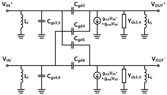
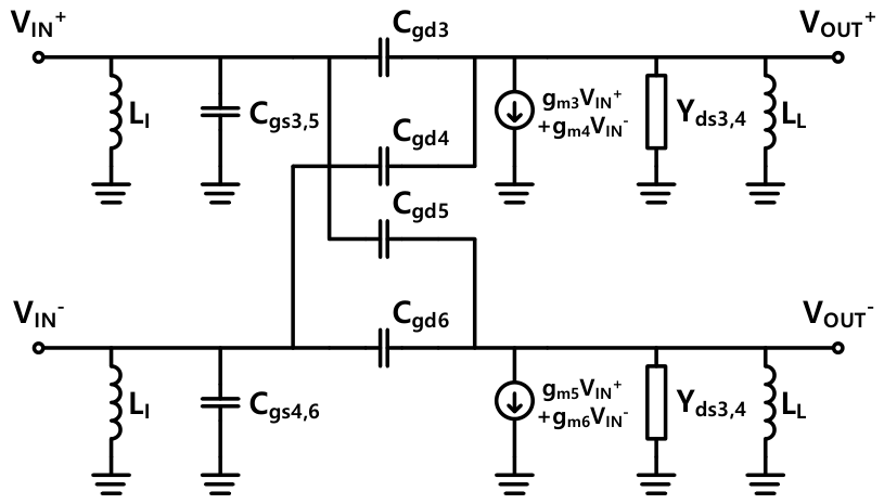
Unlike conventional VGAs that dump unused current into an ac ground, the proposed architecture utilizes a complementary cross-coupled structure to control the gain while maintaining identical parasitic capacitances. Furthermore, the current pathing through M3–M6 is reused for M1 and M2, and M3–M6 are operated as common-source amplifiers. As shown in Figure 1 and Figure 5, the positive input signal VIN+ is fed to the gates of M3 and M5, while the negative input signal VIN− is fed to M4 and M6. The drains of M3 and M4 are tied together to drive the positive output node VOUT+, and the drains of M5 and M6 jointly drive the negative output node VOUT−. By adjusting the bias voltages of the main and steering transistors in a complementary manner, the effective transconductance is controlled by subtracting the out-of-phase current from the in-phase current. Because the sum of the gate capacitances at each node (e.g., Cgs3 + Cgs5 at VIN+) remains nearly constant across all gain states, the input impedance looking into the IIVG stage does not change.
Figure 5.
Simplified small-signal equivalent circuit of the proposed IIVG stage.
To mathematically verify this phase-invariant characteristic, the small-signal equivalent circuit of the proposed IIVG stage is illustrated in Figure 5. Based on this equivalent circuit, the voltage gain AV, IIVG at the positive half-circuit can be derived as follows:
where gm3 and gm4 represent the transconductances of the main and steering transistors, respectively, and Cgd3 and Cgd4 are their corresponding gate-to-drain parasitic capacitances. The term Yds3,4 denotes the combined output admittance, and LL represents the load inductance from the inter-stage transformer.
Based on (1), the phase response of the IIVG stage is determined by the difference between the phase of the numerator and the phase of the denominator. Since the denominator represents the invariant input and output impedances, its phase remains constant across all gain states. Therefore, any phase variation during gain tuning originates solely from the numerator. The phase angle of the numerator can be expressed as:
In the proposed design, the main and steering transistors M3 and M4 are identically sized to ensure physical symmetry. As a result, their parasitic gate-to-drain capacitances are virtually equal, . Applying this condition to (2), the imaginary part of the numerator becomes identically zero, leading to:
Because is maintained near zero regardless of the transconductance difference , the total phase variation between any two gain states intrinsically approaches zero . This rigorous mathematical derivation proves that the proposed cross-coupled IIVGA architecture effectively suppresses parasitic phase shifts, ensuring an exceptionally low phase variation across the entire gain control range. Now, the gain of the IIVG stage under is reduced to
According to (4), the voltage gain of the IIVG stage is solely determined by the effective transconductance difference, . Moreover, owing to the proposed transformer-based current-reuse scheme, this gain control is performed without additional dc power consumption, as the bias current is completely reused between the stacked stages. During operation, the gain is continuously tuned by complementarily adjusting the dc gate bias voltages, VGP and VGN, in Figure 1. Because this complementary current-steering mechanism structurally keeps the sum of the parasitic capacitances constant across all nodes, the VGA can achieve significant gain attenuation without altering the input and output impedances. This unique characteristic ensures that the wideband impedance matching and the insertion phase remain completely invariant across the entire gain tuning range.
Based on this theoretical small-signal analysis, the parameter selection procedure was meticulously conducted to optimize both phase invariance and power efficiency. To mathematically eliminate the phase variation according to (2) and (3), it is strictly required to equalize the intrinsic parasitic gate-to-drain capacitances . Therefore, the main and steering transistors M3–M6 were selected to have identical widths of 39 μm. To optimize the gain, linearity, and power consumption, a quiescent current of 7.4 mA was selected.
Table 1 summarizes the transistor design parameters of the proposed VGA. All transistors employ a channel length of 65 nm. The total transistor width of the input stage (M1–M2), IIVG stage (M3–M6), and output stage (M7–M8) is 50 μm, 39 μm, and 50 μm, respectively. The input and output stages are biased at 0.47 V and 0.42 V, respectively, while the IIVG stage employs a bias voltage ranging from 0.815 V to 1.0 V to achieve gain control through current steering. Owing to the current-reuse architecture, the input stage shares the same quiescent current of 7.4 mA with the IIVG stage. The output stage consumes a quiescent current of 7.6 mA.
Table 1.
The transistor design parameter of the proposed VGA.
2.5. Post-Layout Simulation Performance
To rigorously verify the feasibility and effectiveness of the proposed architecture, comprehensive post-layout simulations were performed, fully incorporating the parasitic extraction of the active devices and the 3-D EM models of all passive components, including transformers, custom MOM capacitors, and routing lines.
Operating under a 1-V supply voltage, the proposed VGA consumes a total dc current of only 15 mA. This highlights the excellent power efficiency achieved by the transformer-based current-reuse topology. The simulated maximum forward gain is 11.46 dB, exhibiting a wide 3-dB bandwidth of 9.5 GHz. Excellent wideband matching is also achieved, with both input and output return losses maintained below 10 dB across the target frequencies.
In terms of beam-tapering capabilities, the VGA provides a continuous gain control range of 20 dB over the entire 50–67 GHz band. More importantly, thanks to the mathematically verified impedance-invariant cross-coupled structure, the RMS phase error is strictly suppressed to less than 1.24°, and the RMS gain error is kept exceptionally low at under 0.13 dB across all gain states.
3. Results
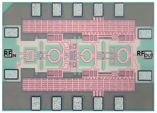
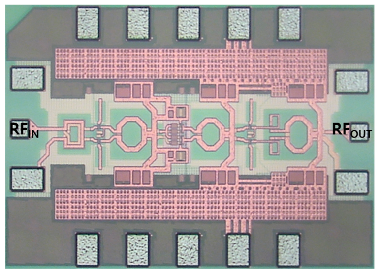
The proposed VGA core was fabricated using a standard 65 nm CMOS process. As depicted in the chip micrograph in Figure 6, the entire circuit occupies a compact footprint of 0.74 × 0.52 mm2, including all RF pads. Operating from a nominal 1.0-V supply, the complete VGA circuit draws a total dc power of only 15 mW.
Figure 6.
Microphotograph of proposed VGA.
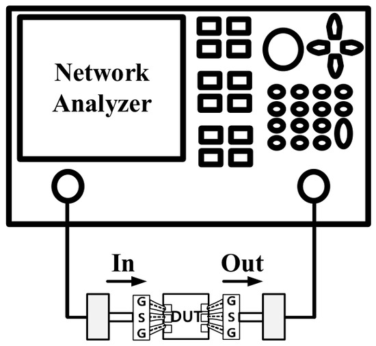
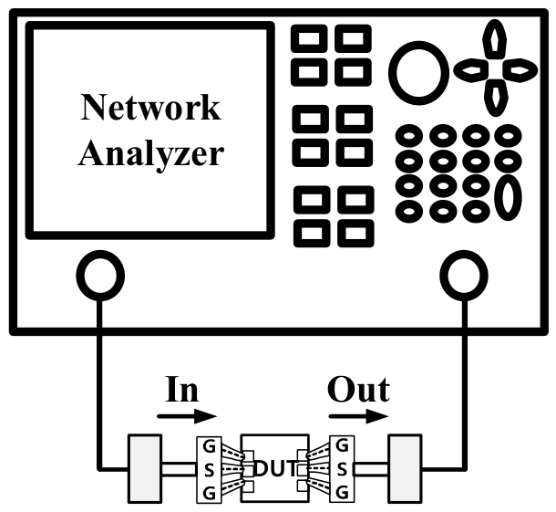
Figure 7 presents the measurement setups utilized for evaluating the S-parameters and large-signal power-handling capabilities. The fabricated chip was characterized via on-wafer probing using a standard ground-signal-ground (GSG) probe configuration to minimize parasitic effects. Both the wideband S-parameters and the input 1-dB compression point (IP1dB) were precisely captured using a Keysight E8361A vector network analyzer (VNA).
Figure 7.
Measurement setup.
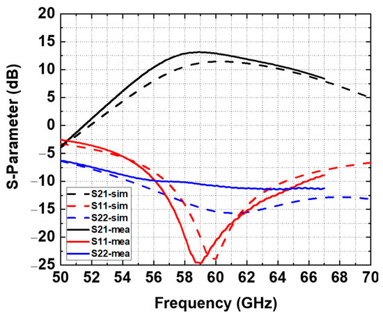
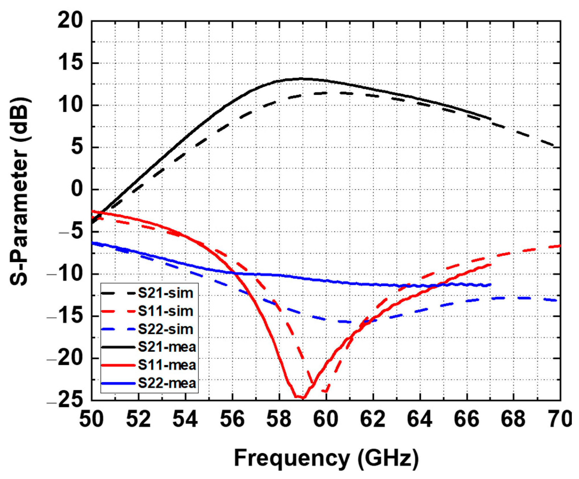
Figure 8 compares the measured and simulated S-parameters of the proposed VGA at the maximum gain setting. The measured gain achieves a peak of 13.2 dB, which is slightly higher than the simulated value of 11.5 dB. The measured 3-dB bandwidth is 8.9 GHz, covering from 55.9 GHz to 64.8 GHz. This demonstrates wideband characteristics, and the overall frequency response shows good agreement with the post-layout simulation results. The discrepancy between the measured and simulated S22 is mainly due to imperfect modeling of the parasitic capacitances in the output RF test pads and routing lines.
Figure 8.
Measured and simulated S-parameters of proposed VGA at maximum gain.
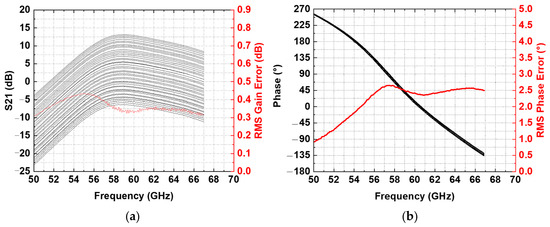
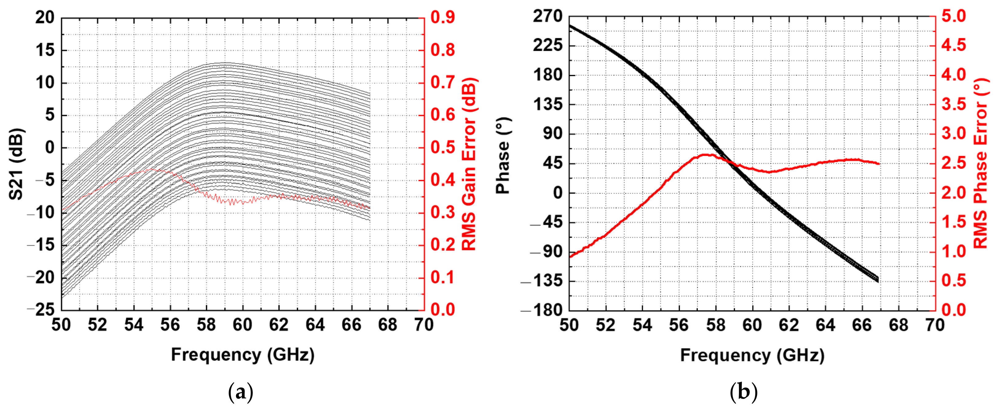
Figure 9 illustrates the measured gain, relative phase shift, and their corresponding RMS errors across various gain settings over the 50–67 GHz band. As shown in Figure 9a, the proposed circuit provides a wide and continuous gain control range of 20 dB, ranging from −3.8 dB to 13.2 dB. Across this entire tuning range, the RMS gain error is maintained below 0.43 dB. Furthermore, as depicted in Figure 9b, the phase variation caused by gain adjustment is successfully suppressed. Thanks to the proposed impedance-invariant cross-coupled topology, the measured RMS phase error remains below 2.65° over the broad 50–67 GHz band. This low phase variation verifies that the proposed VGA can effectively prevent unwanted beam-squinting or pointing errors during the gain-tapering process in phased-array systems.
Figure 9.
Measured (a) gain and RMS gain error, and (b) relative phase shift and RMS phase error for various gain settings.
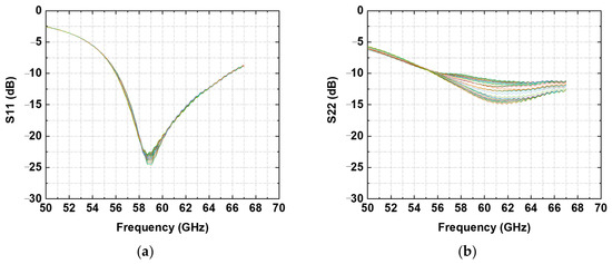
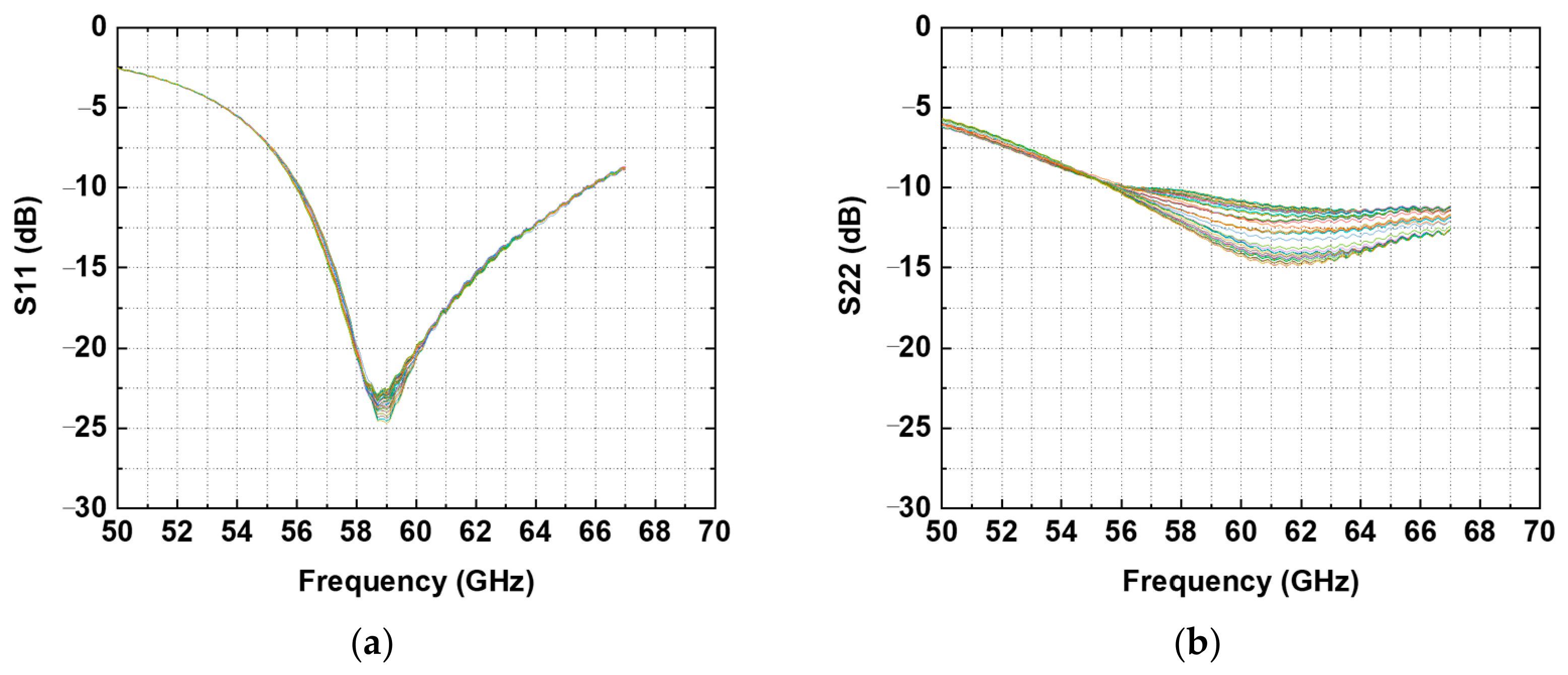
Figure 10 presents the measured input and output return losses for various gain settings. Despite the wide 20 dB gain variation, both the input and output return losses securely remain better than 10 dB across the frequencies of interest, as shown in Figure 10. This verifies that the core design principle—maintaining a constant input and output impedance during gain tuning—functions flawlessly in the actual silicon implementation.
Figure 10.
Measured return losses for various gain settings: (a) input and (b) output.
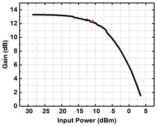
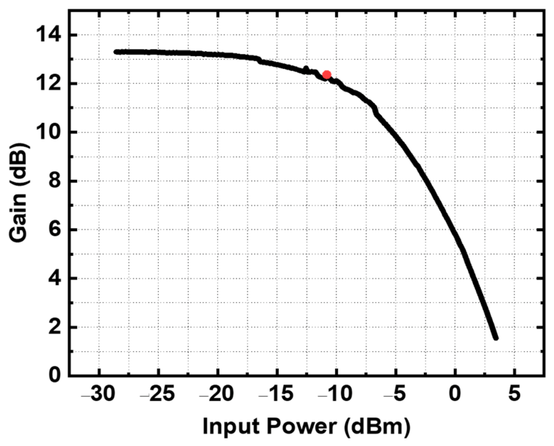
Figure 11 illustrates the measured input 1 dB compression point (IP1dB) at 59 GHz. The measured input 1 dB compression point (IP1dB) is −11 dBm, securing adequate linearity for the target applications. These measurement results confirm that the proposed VGA is a robust, area-efficient, and power-efficient solution for highly integrated millimeter-wave beamforming transceivers.
Figure 11.
Measured input 1 dB compression point (red dot) at 59 GHz.
4. Discussion
Table 2 compares the performance of state-of-the-art millimeter-wave CMOS VGAs [18]. For the performance comparison of the VGAs, the figure-of-merit (FoM) is defined as
Table 2.
Performance comparison of state-of-the-art millimeter-wave VGAs.
A millimeter-wave VGA for phased-array beamforming systems should simultaneously achieve a wide gain control range, low phase variation, moderate-to-high gain, adequate linearity, and low power consumption. However, these performance parameters inherently involve trade-offs, and state-of-the-art VGAs typically prioritize only two or three key aspects. For instance, the IIVGA in [13] demonstrates a high gain of 22.5 dB and a low RMS phase error of 1.4–2.1°; however, it suffers from a significantly high dc power consumption of 67.2 mW. Similarly, the current-steering VGA in [13] provides a high gain of 20 dB, but it exhibits poor linearity with an IP1dB of −15.6 dBm and consumes 38.4 mW. The design in [11] consumes only 5 mW, but it results in a low gain of −3.8 dB and a relatively large phase error of 3–7°. Furthermore, the shunt CS-CG topology in [15] achieves a good gain of 14.4 dB but consumes an extremely high power of 126 mW and provides a limited gain control range of 12.8 dB.
The proposed VGA, which incorporates a transformer-based current-reuse technique and an impedance-invariant cross-coupled topology, successfully overcomes these trade-offs. It achieves a substantial gain of 13.2 dB and a wide gain control range of 20 dB, while tightly maintaining an RMS phase error of less than 2.65° and an RMS gain error of 0.43 dB. Moreover, it achieves an IP1dB of −11 dBm while consuming only 15 mW of dc power, highlighting superior power efficiency compared to most high-gain VGAs. As a result, the proposed VGA demonstrates a highly competitive FoM compared to most prior art, successfully combining a low RMS phase error, low power consumption, high forward gain, and a wide gain control range. Although other VGAs, such as those in [11,18], show numerically higher FoMs, their applicability is compromised; the design in [11] results in a negative gain of −3.8 dB, and the VGA in [18] exhibits limited power-handling capabilities. The measurement results summarized in Table 1 indicate that the proposed VGA is well-suited for 60 GHz low-power millimeter-wave handheld devices and phased-array systems, offering an optimal balance among gain, phase invariance, linearity, and power efficiency.
5. Conclusions
This paper presented a 60 GHz high-gain, low-phase-error VGA designed in a 65 nm CMOS process for millimeter-wave phased-array beam-forming systems. To fundamentally overcome the inherent trade-off between power consumption and forward gain, a transformer-based current-reuse technique was successfully implemented. This technique enables the input and variable gain stages to efficiently share the dc bias current, achieving a highly efficient power consumption of only 15 mA from a 1 V supply. Furthermore, an impedance-invariant cross-coupled topology was proposed to suppress parasitic phase shifts during the gain control. The mathematical derivation and post-layout simulation results verify that this topology successfully minimizes the phase error. Operating within the 50–67 GHz band, the proposed VGA provides a continuous gain control range of 20 dB with a maximum gain of 13.2 dB. Across the entire tuning range, the RMS phase error is less than 2.65°, and the RMS gain error is below 0.43 dB. The VGA also exhibits an adequate IP1dB of −11 dBm while occupying a highly compact area of 0.38 mm2. These measurement results confirm that the proposed VGA offers a robust, area-efficient, and power-efficient solution for precise beam tapering in next-generation 60 GHz phased-array transceivers.
Author Contributions
Conceptualization, C.-W.B. and I.-C.Y.; data curation, C.-W.B. and I.-C.Y.; formal analysis, C.-W.B. and I.-C.Y.; investigation, C.-W.B.; funding acquisition, C.-W.B.; methodology, C.-W.B. and I.-C.Y.; project administration, C.-W.B.; resources, C.-W.B.; software, C.-W.B. and I.-C.Y.; supervision, C.-W.B.; validation, C.-W.B. and I.-C.Y.; visualization, C.-W.B. and I.-C.Y.; writing—review and editing, C.-W.B. and I.-C.Y.; writing—original draft, I.-C.Y. All authors have read and agreed to the published version of the manuscript.
Funding
The present research was supported by the research fund of Dankook University in 2025.
Data Availability Statement
Data are contained within this article.
Conflicts of Interest
The authors declare no conflicts of interest.
References
- So, C.; Sung, E.-T.; Hong, S. A V-Band four-channel phased array transmitter front-end with 0.7° phase step and 20 dB gain dynamic range. IEEE Trans. Microw. Theory Tech. 2024, 72, 2799–2808. [Google Scholar]
- Kiani, S.H.; Altaf, A.; Anjum, M.R.; Afridi, S.; Arain, Z.A.; Anwar, S.; Khan, S.; Alibakhshikenari, M.; Lalbakhsh, A.; Khan, M.A.; et al. MIMO Antenna System for Modern 5G Handheld Devices with Healthcare and High Rate Delivery. Sensors 2021, 21, 7415. [Google Scholar] [CrossRef] [PubMed]
- Mayeda, J.; Lie, D.Y.C.; Lopez, J. Broadband Millimeter-Wave 5G Power Amplifier Design in 22 nm CMOS FD-SOI and 40 nm GaN HEMT. Electronics 2022, 11, 683. [Google Scholar] [CrossRef]
- Hussain, S.A.; Taher, F.; Alzaidi, M.S.; Hussain, I.; Ghoniem, R.M.; Sree, M.F.A.; Lalbakhsh, A.L. Wideband, High-Gain, and Compact Four-Port MIMO Antenna for Future 5G Devices Operating over Ka-Band Spectrum. Appl. Sci. 2023, 13, 4380. [Google Scholar]
- Song, J.-H.; Lee, E.-G.; Lee, J.-E.; Son, J.-T.; Kim, J.-H.; Baek, M.-S.; Kim, C.-Y. A 37–40 GHz 6-Bits Switched-Filter Phase Shifter Using 150 nm GaN HEMT. Nanomaterials 2023, 13, 2752. [Google Scholar] [PubMed]
- Kankuppe, A.; Park, S.; Renukaswamy, P.T.; Wambacq, P.; Craninckx, J. A wideband 62-mW 60-GHz FMCW radar in 28-nm CMOS. IEEE Trans. Microw. Theory Tech. 2021, 69, 2921–2935. [Google Scholar] [CrossRef]
- Park, G.H.; Park, C.S.; Jang, T.H. Dual Polarization Dynamic Alignment of Integrated Phased Arrays. IEEE J. Solid-State Circuits 2025, 60, 1681–1693. [Google Scholar]
- Lee, J.G.; Jang, T.H.; Park, G.H.; Lee, H.S.; Byeon, C.W.; Park, C.S. A 60-GHz four-element beam-tapering phased-array transmitter with a phase-compensated VGA in 65-nm CMOS. IEEE Trans. Microw. Theory Tech. 2019, 67, 2998–3009. [Google Scholar]
- Jung, K.P.; Jang, T.H.; Kim, J.H.; Park, C.S. A 60-GHz power-efficient four-element CMOS phased-array transmitter with 31-dBm peak EIRP for short-range Gb/s wireless transmission. IEEE Trans. Microw. Theory Tech. 2024, 72, 3452–3467. [Google Scholar]
- Wu, T.; Zhao, C.; Liu, H.; Wu, Y.; Yu, Y.; Kang, K. A 20–43 GHz VGA with 21.5 dB gain tuning range and low phase variation for 5G communications in 65-nm CMOS. In Proceedings of the 2019 IEEE Radio Frequency Integrated Circuits Symposium (RFIC), Boston, MA, USA, 2–4 June 2019; IEEE: New York, NY, USA, 2019; pp. 71–74. [Google Scholar]
- Park, G.H.; Byeon, C.W.; Park, C.S. A 60-GHz Low-Power Active Phase Shifter with Impedance-Invariant Vector Modulation in 65-nm CMOS. IEEE Trans. Microw. Theory Tech. 2020, 68, 5395–5407. [Google Scholar]
- Li, X.; Cheng, D.; Jiang, X.; Wang, D.; Li, L. A 57–71-GHz Accurate dB-Linear Variable Gain Power Amplifier with Ultralow Gain Error Using Particle Swarm Optimization Algorithm. In Proceedings of the 2024 IEEE MTT-S International Microwave Symposium (IMS), Washington, DC, USA, 16–21 June 2024; IEEE: New York, NY, USA, 2024; pp. 454–457. [Google Scholar]
- Chen, X.; Cheng, D.; Ma, X.; Feng, J.; Chen, Q.; Wu, X.; Fan, X.; Li, L. A 60-GHz Phase-Invariant Variable Gain LNA With T/R Switch and Gain Interpolation Techniques in 65-nm CMOS. IEEE Microw. Wirel. Tech. Lett. 2024, 34, 508–511. [Google Scholar]
- Wang, H.; Huang, T.; Hu, Z.; Cao, H.; Wu, W. A Ka-Band Gm-Boosted PS-VGA With Low Phase Variation by Main-Path Inductor Compensation. IEEE Microw. Wirel. Tech. Lett. 2025, 35, 577–580. [Google Scholar]
- Meng, S.; Yu, Y.; Xiao, L.; Zhao, C.; Wu, Y.; Liu, H.; Kang, K. A Single-Ended Phase and Impedance Invariant mm-Wave VGPA Based on Shunt CS-CG Topology. IEEE Trans. Circuits Syst. I Reg. Pap. 2025, 72, 1987–2000. [Google Scholar]
- Lee, C.J.; Nam, H.; Kim, D.; Kim, S.-K.; Lee, D.Y. A D-band variable gain low noise amplifier in a 28-nm CMOS process for 6G wireless communications. IEEE Trans. Circuits Syst. II Exp. Briefs 2024, 71, 131–135. [Google Scholar]
- Wei, Q.; Yang, C.; Liu, X.; Wang, Y.; Jin, J.; Zhou, J. A Millimeter-Wave Two-Way Series-Doherty Power Amplifier with Transformer-Based Second-Order Output Network. IEEE Trans. Microw. Theory Tech. 2026, 74, 4296–4309. [Google Scholar]
- Siao, D.-S.; Kao, J.-C.; Wang, H. A 60 GHz low phase variation variable gain amplifier in 65 nm CMOS. IEEE Microw. Wirel. Compon. Lett. 2014, 24, 457–459. [Google Scholar] [CrossRef]

Disclaimer/Publisher’s Note: The statements, opinions and data contained in all publications are solely those of the individual author(s) and contributor(s) and not of MDPI and/or the editor(s). MDPI and/or the editor(s) disclaim responsibility for any injury to people or property resulting from any ideas, methods, instructions or products referred to in the content. |
© 2026 by the authors. Licensee MDPI, Basel, Switzerland. This article is an open access article distributed under the terms and conditions of the Creative Commons Attribution (CC BY) license.