


Abstract
Analog in-memory computing (AIMC) has emerged as a promising approach to mitigate the Von Neumann bottleneck in matrix operations, which are common in deep learning applications. However, the practical implementation of resistive crossbar arrays is limited by challenges in signed weight representation, conductance quantization, and device nonlinearity. This paper presents a differential mixed-signal architecture for accurate signed matrix–vector multiplication (MVM), integrated with a RISC-V microcontroller for edge inference applications. A structured digital-to-analog mapping framework encodes quantized neural network weights into programmable conductance values while preserving arithmetic correctness. The design employs voltage-mode input encoding, differential current summation, and transimpedance-based readout followed by analog-to-digital conversion, enabling single-cycle signed accumulation without duplicating crossbar resources. A 32 × 16 dual-layer prototype crossbar was fabricated and experimentally characterized. Measurements demonstrate a mean absolute percentage error (MAPE) below 1% within the linear operating region and below 4% over the full-scale conductance range. These results validate the robustness of the proposed mapping methodology and confirm the feasibility of hybrid analog–digital acceleration for edge AI systems. Consequently, this discrete prototype serves as a physical verification platform for the AIMC approach, providing valuable insights for more efficient mixed-signal computing integrated circuit (IC) designs.
1. Introduction
The rapid proliferation of artificial intelligence (AI) in edge applications, including the Artificial Intelligence of Things (AIoT), robotics, and electric vehicles, has initiated a new era characterized by intelligent, real-time, and context-aware devices and services. These applications necessitate the deployment of advanced deep learning models and data-driven algorithms directly on resource-constrained edge devices, thereby enabling low-latency decision-making and reducing reliance on cloud-based processing. Although high-end central processing units (CPUs) and graphics processing units (GPUs) serve as powerful workhorses for real-time computing, their substantial power consumption and enormous operating current [1] render them unsuitable as the ultimate solution for most edge applications, where energy efficiency, thermal constraints, and form factor limitations are critical. Furthermore, as AI models become increasingly complex and large-scale, their computational requirements imposed on edge hardware have increased dramatically, revealing fundamental constraints in existing digital architectures, particularly in terms of power efficiency and latency for matrix-dominated operations.
Edge AI refers to the execution of AI algorithms, particularly deep neural networks (DNNs), on devices situated near the data source, such as sensors, mobile devices, and embedded systems, rather than centralized cloud data centers. This shift in paradigm is driven by the need for real-time responsiveness, privacy protection, and reduced network congestion in applications that range from autonomous vehicles and industrial automation to smart healthcare and intelligent transportation systems [2,3,4]. At the core of these AI workloads are heavy matrix operations, especially matrix–vector and matrix-matrix multiplications, which form the core computations in neural network inference and training [3,5,6].
Traditional digital architectures, such as CPUs, GPUs, and even specialized AI accelerators, are fundamentally limited by the division between memory and computation. This phenomenon, known as the “von Neumann bottleneck,” results in considerable energy consumption and latency due to the frequent transfer of data between memory and processing units, particularly during matrix-intensive operations [5,6]. Given that edge devices are inherently constrained in terms of power, memory, and thermal capacity, these inefficiencies pose significant obstacles to the deployment of large-scale AI models at the network edge [2,4,7]. For instance, deep learning inference on edge devices is often computationally demanding and energy-intensive, necessitating millions of parameters and iterative operations. Consequently, the majority of AI models are conventionally executed in the cloud. However, cloud-centric deployment introduces high latency, privacy issues, and reliance on stable connectivity—factors that are unacceptable for latency-sensitive and mission-critical edge applications [2,4]. Despite advancements in hardware accelerators, the energy and latency challenges associated with digital matrix computations continue to be a major hurdle [5,6].
The integration of AI and IoT (AIoT) has heightened the demand for efficient edge intelligence. AIoT applications, including smart manufacturing, predictive maintenance, and autonomous navigation, require real-time analysis on massive sensor data streams. Similarly, robotics and electric vehicles require swift perception, planning, and control, all of which depend on fast and energy-efficient matrix computations [2,7,8]. The escalating complexity of AI models, along with the necessity for on-device learning, further intensifies the computational and energy requirements placed on edge hardware [4,8,9].
To address these challenges, researchers have investigated various optimization strategies at both hardware and software levels. These strategies encompass model compression, quantization, algorithm-hardware co-design, and the development of specialized accelerators, including compute-in-memory (CIM) chips and photonic processors [4,5,6,10], as well as custom multipliers [11,12]. For instance, CIM architectures combine memory and computation to reduce data movement, resulting in notable enhancements in energy efficiency and latency for matrix operations [6,10]. Simultaneously, carefully approximated multipliers can achieve an optimal balance between error tolerance and power saving [12].
While emerging hardware paradigms such as CIM and photonic digital computing offer promising directions, a more comprehensive approach is proposed to realize the potential of edge AI fully. This approach incorporates CIM, analog computing matrix, alongside an RISC-V core microcontroller, which entails hardware-software co-design and system-level optimization. Table 1 summarizes how our proposed architecture compares against prior CIM studies:
Table 1.
Features of some recent CIM studies and our proposed architecture.
The subsequent sections are organized as follows. Firstly, it introduces the holistic design that integrates an analog computing matrix with an RISC-V core microcontroller. This is followed by the measurement result. Finally, the paper concludes.
2. Background
2.1. RISC-V
RISC-V distinguishes itself from proprietary Instruction Set Architectures (ISAs), such as Arm and x86, through a combination of technical innovation and strategic advantages that drives its rapid global adoption. As a fully royalty-free, open standard, it eliminates licensing fees and per-unit royalties, greatly reducing barriers for high-volume production. Its modular, extensible design starts with a compact base integer ISA (RV32I/RV64I) of about 50 instructions. Optional standard extensions—for multiplication, atomics, floating-point, vectors, compressed instructions, and bit manipulation—can be added as needed. This allows highly customized cores, from tiny embedded controllers to advanced out-of-order CPUs and vector processors, without the overhead of unused features [15]. The ISA reserves space for custom extensions, enabling domain-specific accelerators (e.g., for AI, cryptography, or signal processing) while preserving compatibility with the base standard [15]. As a clean, modern architecture free of legacy complexity, RISC-V often delivers simpler and more energy-efficient designs than older proprietary alternatives. Crucially, in today’s geopolitical environment, its open nature provides a path to semiconductor independence—a major adoption driver worldwide.
These strengths have led to broad commercial and research use, with over two billion RISC-V SoCs shipped in 2024. Forecasts project this figure to reach 20 billion SoCs by 2031, mainly in storage controllers, microcontrollers, and IoT devices [16]. Consequently, RISC-V has matured from an academic project into a globally competitive ISA, challenging proprietary architectures across the entire computing spectrum.
2.2. Analog Matrix Computing
Analog Matrix Computing (AMC) revives analog computing by using continuous physical signals (voltages, currents) to perform matrix operations—such as multiplication, inversion, pseudoinverse, and eigenvector computation—in a single, highly parallel step, avoiding digital binary abstractions [17]. Unlike von Neumann systems, where the “memory wall” causes energy-intensive data movement, AMC embeds computation directly within memory arrays, slashing latency, power, and area for data-heavy tasks in machine learning, scientific simulations, wireless communications, and signal processing.
AMC executes key linear-algebra operations—notably MVM, inversion, and pseudoinverse—directly in the analog domain with continuous variables. By integrating computation into the storage medium, it eliminates repeated data transfers, achieving O(1) time complexity for core operations regardless of matrix size [18,19]. The primary hardware is the memristive crossbar array, where matrix values are stored as conductance in resistive devices (RRAM, PCM, or ferroelectric transistors). Applying input voltages to the rows produces output currents along the columns, instantly computing the matrix–vector product via Kirchhoff’s and Ohm’s laws. More advanced tasks, like solving Ax = b, use iterative analog feedback loop networks or block-wise algorithms that converge quickly in continuous time [18].
Recent architectural advances have significantly narrowed the precision and scalability gap between analog and digital systems. For instance, a 2025 memristive prototype delivered a 24-bit fixed-point equivalent accuracy for 16 × 16 matrix inversion, with 1000× higher throughput and 100× lower energy than top GPUs, scaling to 128 × 128 arrays in just three iterations [20]. These results illustrate that AMC is a strong post-Moore candidate for energy-constrained edge AI applications.
3. Design and Architecture
3.1. Calculation Algorithms
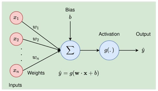
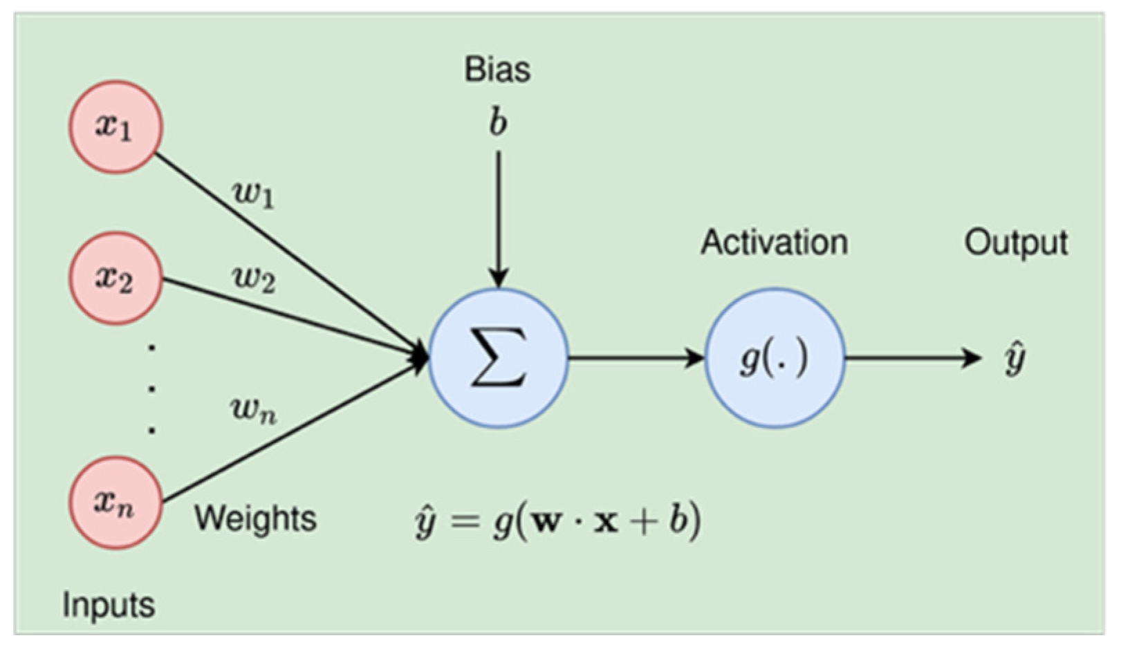
In a neural network (NN), a neuron serves as the fundamental computational unit. As shown in Figure 1, it processes inputs (xn) using learned weights (wn). The neuron first calculates a weighted sum, z, via a dot product, as expressed in Equation (1):
z = w1x1 + w2x2 + … + wnxn
Figure 1.
A neuron in neural network.
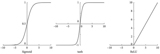
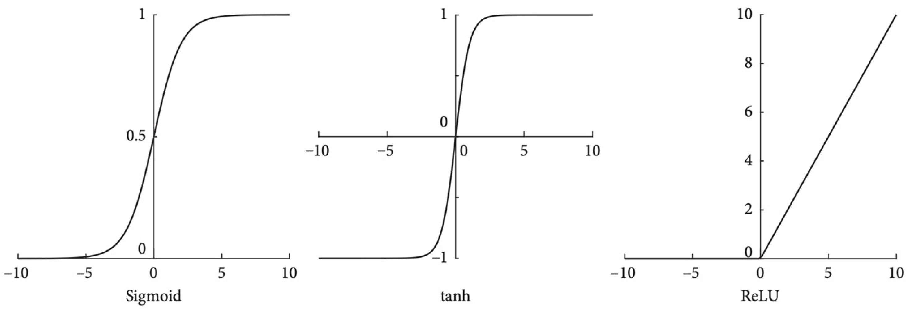
A bias term (b) is then added: z = z + b. To produce the final output for the subsequent layer or network delivery, this result passes through a non-linear activation function (e.g., ReLU, sigmoid, or tanh, depicted in Figure 2). Consequently, the final output of a single neuron is represented by Equation (2):
z = g (w1x1 + w2x2 + … + wnxn + b)
Figure 2.
Three different activation functions.
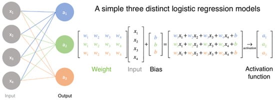
A simple NN architecture, illustrated in Figure 3, consists of multiple neurons organized into layers, featuring four inputs and three outputs. The collective output of this network is described in Equation (3):
Figure 3.
A simple network model.
Assuming a uniform activation function throughout the network, this formulation can be simplified into the matrix form shown in Equation (4):
Equation (4) is further simplified to Equation (5):
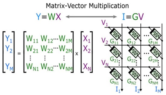
which is an MVM calculation—the most computationally intensive step in the network. Neurons enable NNs to infer complex patterns, with the input-weight multiplications modeled by analog circuits, as illustrated in Figure 4.
Figure 4.
MVM conversion diagram.
Using Ohms’ Law (Equation (6)), inputs (X) are represented by voltage (V), weights (W) by conductance (G = 1/R), and the output (Y) by current (I). The total output current is then summed according to Kirchhoff’s Current Law (Equation (7)).
3.2. 32 × 16 Differential MVM Calculate Circuit
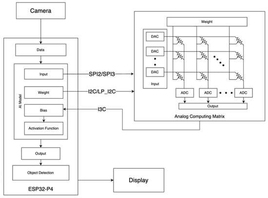
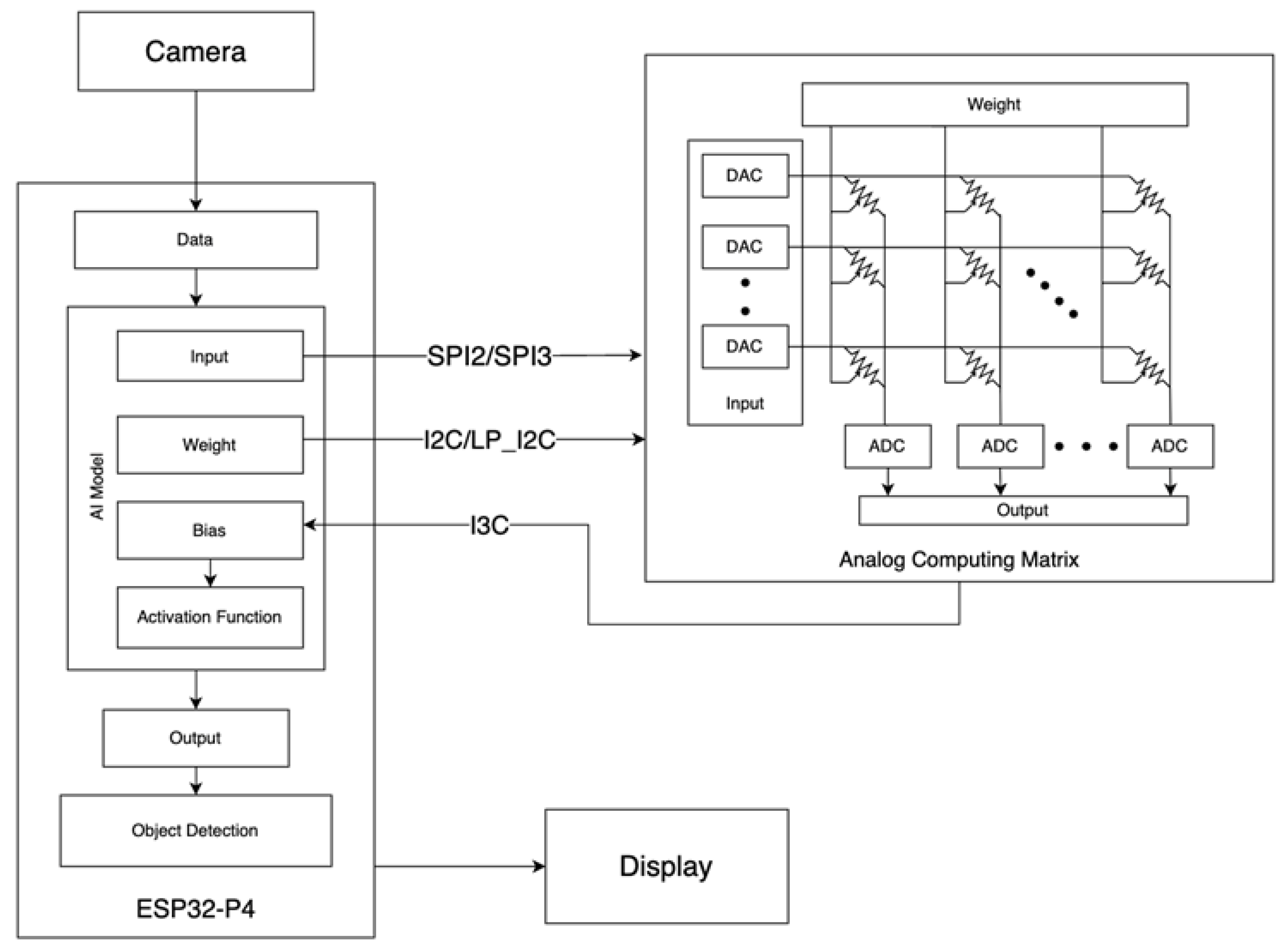
To validate the design concept, a 32 × 16 × 2 analog computing matrix was designed and fabricated on a printed circuit board (PCB) based on the previous equations. Weights are implemented as resistances using MCP4452 digital potentiometers (manufactured by Microchip, sourced from Hong Kong), which are configured by an MCU via an I2C interface. Each column’s output current is converted to a voltage using LM324DR as transimpedance amplifier (TIA) (manufactured by Texas Instruments, sourced from Shenzhen, China) and summed to produce the final output. Figure 5 shows the full mixed-signal system architecture.
Figure 5.
System function block.
The system uses an Espressif ESP32-P4 RISC-V microcontroller to manage the inference pipeline and peripherals. Real-time images come from a MIPI-CSI camera. The ESP32-P4 handles data preprocessing and runs inference on non-accelerated model layers. Conversely, compute-intensive layers are offloaded to the analog matrix: input activations are transmitted via SPI, and weights are configured via I2C. The resulting analog outputs are digitized by ADCs and returned to the microcontroller for bias addition and digital activation functions. This hybrid process repeats layer by layer until the final human-detection results are displayed on a MIPI-DSI screen.
3.2.1. Hardware Architecture
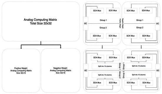
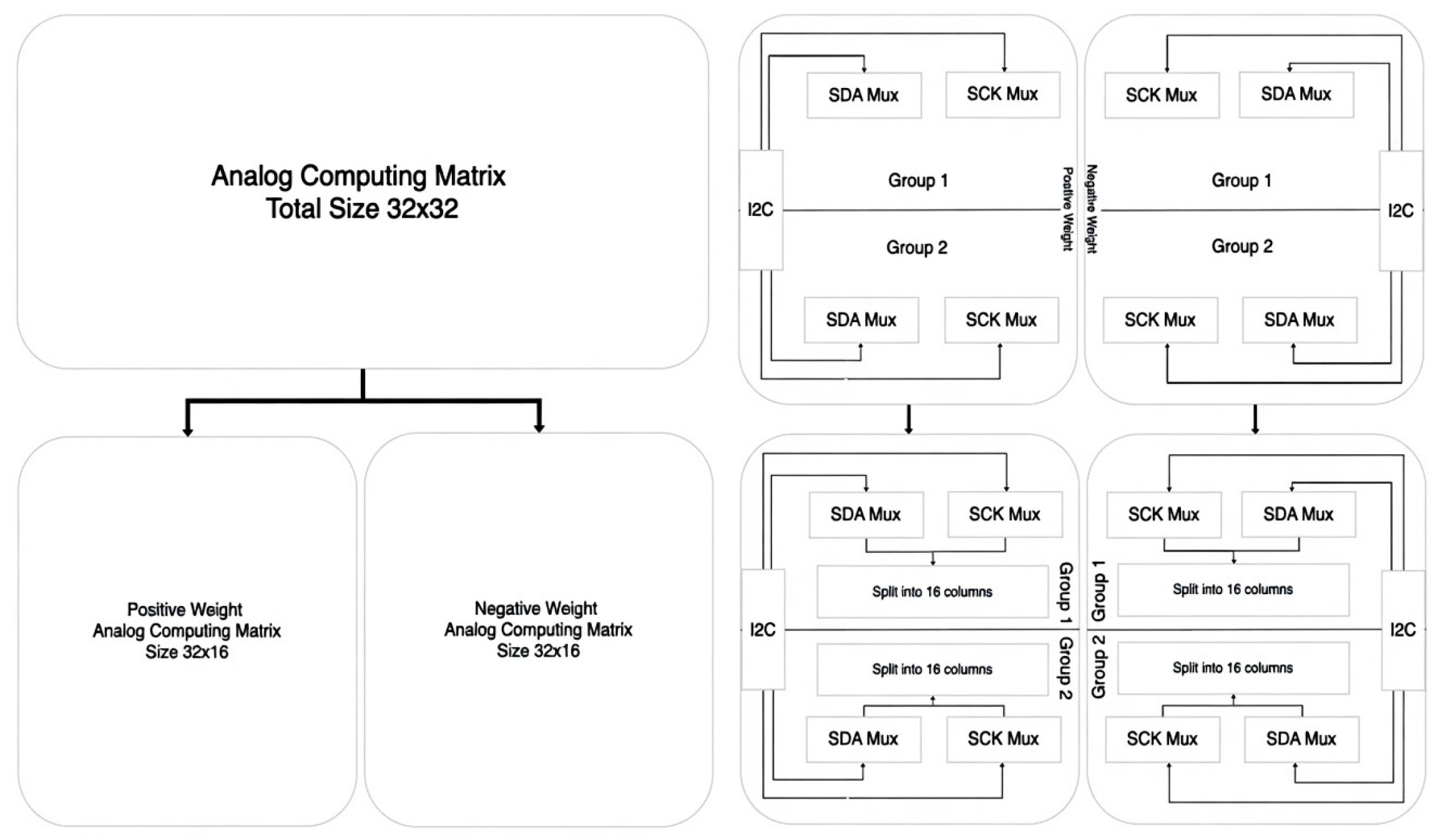
To meet strict printed circuit board assembly (PCBA) cost and footprint constraints, the original 32 × 32 analog computing matrix was redesigned into a partitioned architecture. Because neural network weights can be positive or negative while memristor conductance is inherently non-negative, signed weights are implemented by splitting the computation into two 32 × 16 sub-matrices: one for positive weights and one for the absolute value of negative weights. The resulting currents are subtracted at the output stage using a differential ADC to recover the correct signed MVM result. This design is shown on the left of Figure 6.
Figure 6.
The grouping of cells in an analog computing matrix.
The core advantage of this design is offloading the compute-intensive MVM operations to the proposed analog matrix computing (AMC) circuit. The AMC consists of three main stages:
- Differential weight configuration;
- Analog input processing via DACs;
- Parallel output readout using TIAs and ADCs.
Weight Configuration
ESP32-P4 retrieves layer weights from flash memory and programs them into the analog accelerator’s non-volatile conductance arrays via I2C/LP-I2C (Figure 5). The accelerator has two separate 8 × 16 arrays: one for positive weights, one for negative; signed weights achieved differentially.
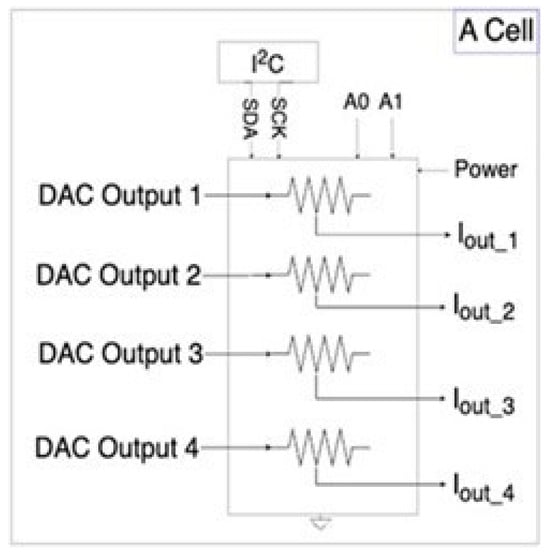
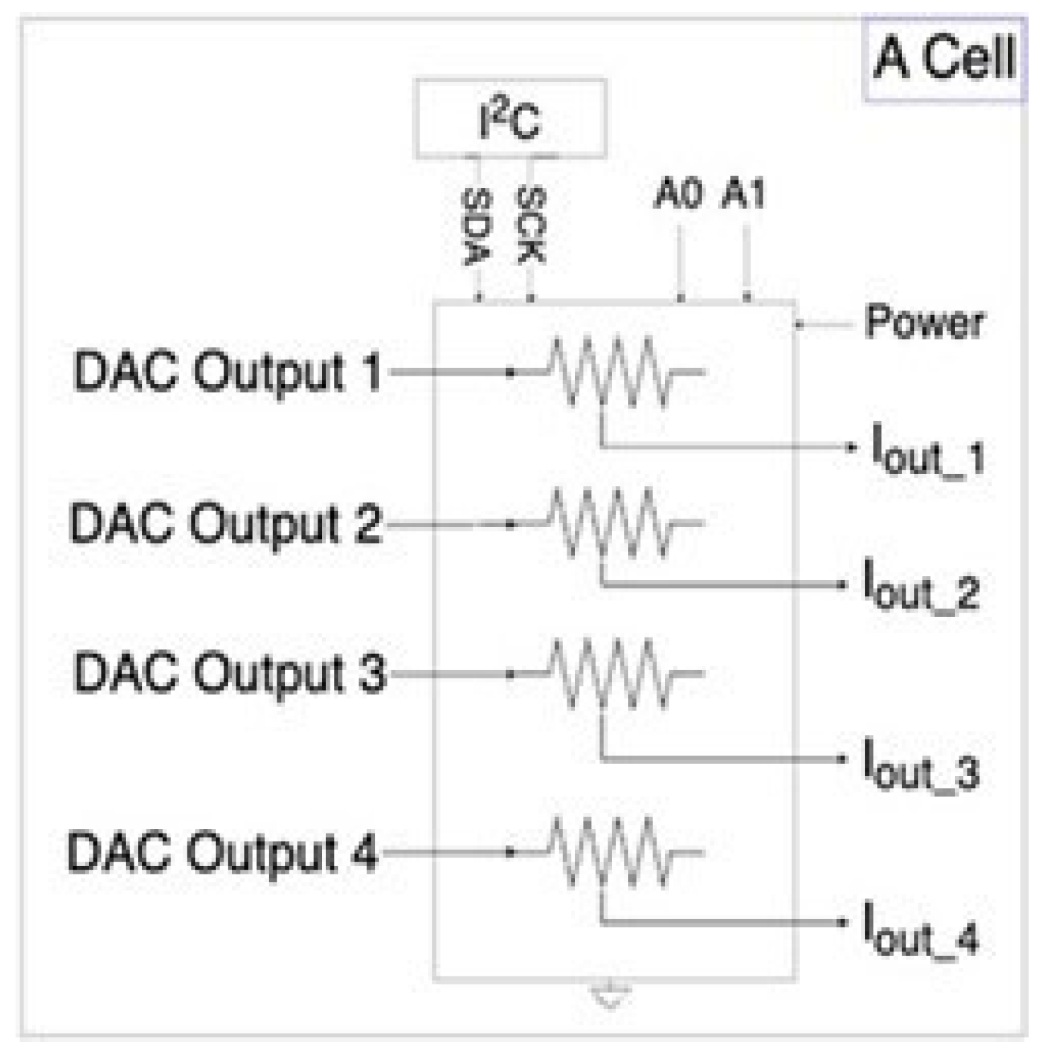
As shown in Figure 7, each cell consists of four I2C-programmable digital potentiometers to encode the absolute weight as conductance value (1/R). Cell selection employs dedicated address pins (A0, A1) combined with 1-to-16 multiplexers driven by SDA and SCK lines (Figure 8).
Figure 7.
The detail of a cell in analog computing matrix.
Figure 8.
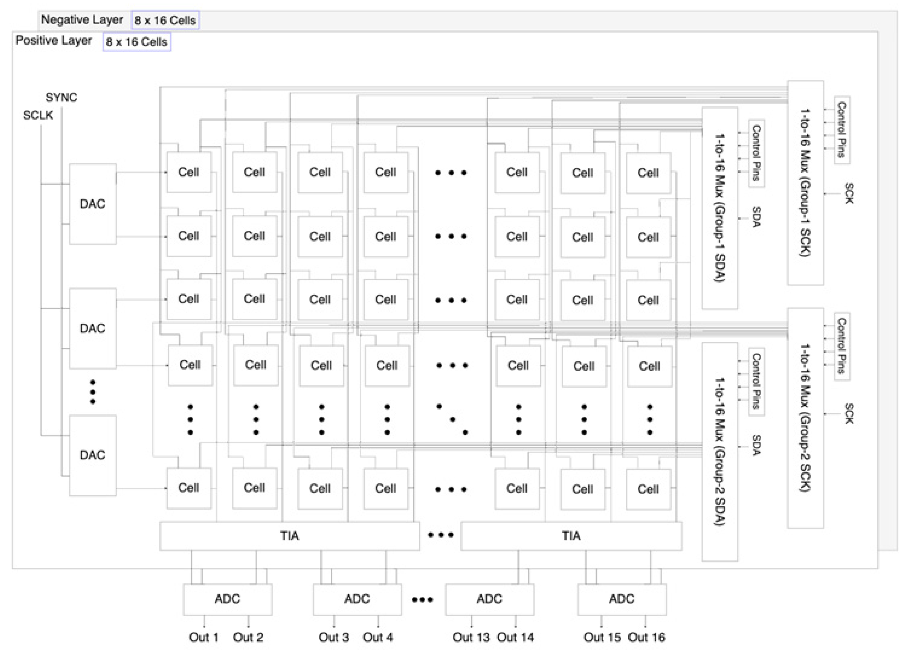
Analog computing matrix MVM computation hardware structure.
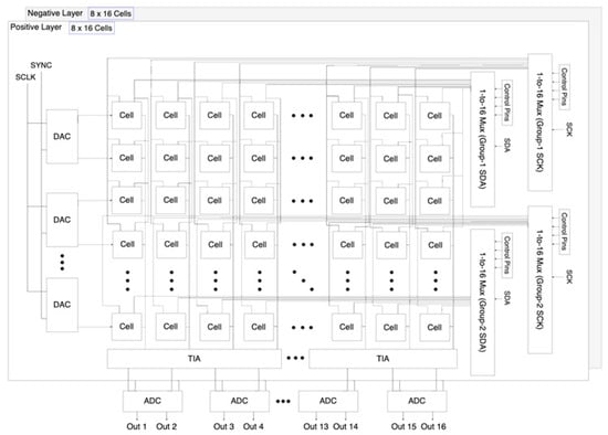
To address the full 8 × 16 array, a hierarchical grouping scheme is implemented (right side of Figure 8). Four cells are grouped into one segment, and 16 segments form one column group. Each 8 × 16 board is partitioned into two such column groups controlled by four multiplexers. This multiplexing strategy enables individual programming of all cells in both signed arrays, allowing for the complete on-the-fly reconfiguration of an entire neural network layer.
Input Vector Streaming
Following weight configuration, the ESP32-P4 streams the preprocessed input activation vector to the analog accelerator via SPI. Dedicated multi-channel DACs convert the digital SPI words into analog voltages Vi, with each DAC output driving a specific matrix row (Figure 7).
MVM is performed in the analog domain at each crosspoint. When row voltage Vi is applied, current Iij flows through the programmed conductance Gij of cell (i,j), directly realizing the multiplication term in accordance with Ohm’s law (Equation (6)) and the core MVM formulation (Equation (8)). Column-wise summation of these currents naturally computes the dot products.
Iij = ViGij
Output Generation and Readout
As in Phase One, column-wise accumulation passively follows Kirchhoff’s Current Law (KCL), where currents from all cells in a column converge onto a shared bitline. Each bitline feeds a dedicated transimpedance amplifier (TIA). This TIA maintains a virtual ground at its inverting terminal for precise summation and converts the aggregated current into a stable voltage Vout,j.
Signed computation is completed by differential ADCs that directly subtract the negative-layer current In,j from the corresponding positive-layer current Ip,j, yielding a digitized output proportional to the true signed dot product. The resulting digital vector is returned to the ESP32-P4 for bias addition, activation, and subsequent layer processing. Equation (9) illustrates the summation of the current of each column, that is, before converting to Vout,j by TIA.
Vout,j = ∑ Vp,j Gp,ij − ∑ Vn,i Gn,ij
3.2.2. AI Model with MobileNetV3 Backbone
To demonstrate the practical applicability of the proposed analog computing matrix in a real-world edge-AI scenario, a human detection task was implemented using a MobileNetV3-based neural network on a power- and memory-constrained RISC-V microcontroller with real-time camera input. This model balances detection accuracy, computational efficiency, and hardware compatibility.
Developed by Google, MobileNetV3 was chosen for its state-of-the-art balance between efficiency and accuracy in on-device inference. Specifically designed for mobile and embedded platforms, it incorporates depthwise separable convolutions, inverted residual blocks, squeeze-and-excitation (SE) modules, and lightweight activations (ReLU, hard-swish). These architectural features greatly reduce computational complexity compared to conventional CNNs while preserving strong performance (Table 2).
Table 2.
The Detail of MobileNetV3 in Each Layer.
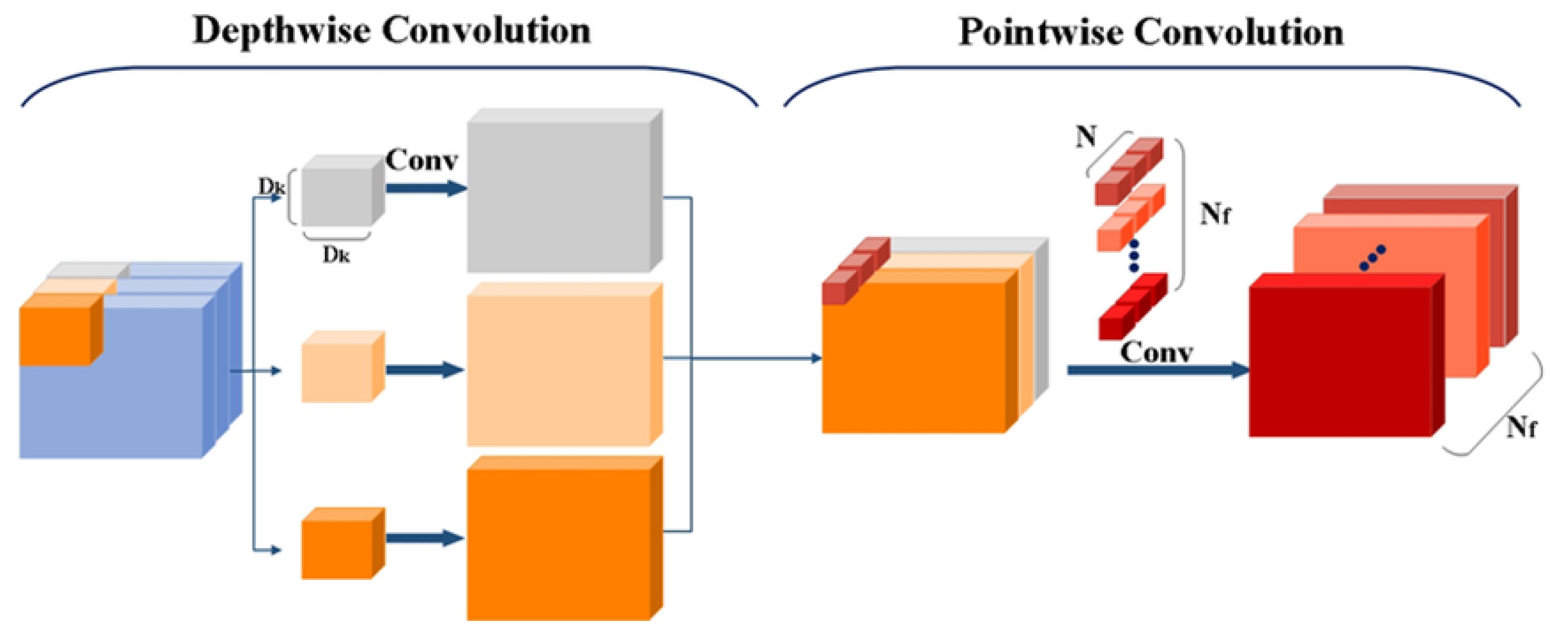
MobileNetV3 achieves its efficiency through depthwise separable convolutions (Figure 9), which decompose a standard convolution into two lower-cost operations: Depthwise convolution and Pointwise convolution.
k2⋯Cin⋯Cout (where k = 3)
k2⋯Cin + Cin⋯Cout (where k = 3)
Figure 9.
The depth-wise convolution and pointwise convolution in MobileNetV3.
Compared to standard convolution (Equation (10)), the separable version (Equation (11)) reduces multiply–accumulate operations by a factor of 8 to 9. Consequently, the digital host offloads one pointwise convolution layer to the analog computing matrix for acceleration.
In MobileNetV3, computational cost is dominated by 1 × 1 pointwise convolutions. While depthwise convolutions perform low-cost spatial filtering per channel, pointwise layers handle dense channel mixing and account for the majority of MAC operations. Each pointwise convolution is mathematically equivalent to an MVM, making it ideal for analog matrix acceleration.
The proposed system uses a hybrid analog–digital strategy: depthwise convolutions and auxiliary layers run digitally on the ESP32-P4 RISC-V microcontroller, whereas one pointwise convolution layer is offloaded to the analog computing matrix.
During inference, quantized MobileNetV3 pointwise weights are programmed into the analog matrix as conductance values via I2C. Input activation vectors are applied through DACs to the matrix rows, where analog current summation computes the dot product in a single step. Outputs are digitized via TIAs and ADCs, followed by digital bias addition, activation, and layer sequencing. This process repeats layer by layer until the final human detection result is obtained.
By offloading pointwise convolutions, the system substantially cuts digital MAC operations and data movement—the main sources of power consumption in edge-AI inference. This MobileNetV3-based human detection pipeline thus demonstrates a practical, scalable integration of analog computing matrices into lightweight neural networks for edge applications.
3.2.3. Electronic Component and Circuit Design
The Phase-Two prototype integrates all mixed-signal subsystems needed to operate the 32 × 16 × 2 analog computing matrix. The following subsections outline the design considerations for each key hardware block: the digital interface, power subsystem, multiplexing architecture, DAC-driven input stage, analog matrix array, and TIA–ADC output chain.
Hardware Circuit Interface
The hardware interface bridges the ESP32-P4 digital host and the analog computing matrix. To simplify high-density PCB routing, the interface is organized into four logical signal groups: SPI, power rails, I2C, and I3C. The ESP32-P4 provides both 3.3 V and 5 V power rails to the analog board, while an additional power supply is used to enhance higher stability and noise isolation. All digital lines share a common ground to ensure signal integrity.
I2C and I3C Multiplexing for Cells and ADC Selection
Because the analog matrix contains a large number of digitally controlled resistive cells, a scalable addressing scheme is necessary. The I2C bus is expanded using the XL4067-SS (manufactured by XINLUDA, sourced from Shenzhen, China), 16-channel analog multiplexer to route the SCL and SDA lines to individual matrix columns. Each column is further divided into two groups, enabling the ESP32-P4 to selectively configure the MCP4452 devices without address conflict. Pull-up resistors are placed on each I2C segment to ensure signal stability during channel transitions.
For the ADC readout path, a CD4052BM96 dual 4-channel MUX (manufactured by Texas Instruments, sourced from Shenzhen, China) is used to route the differential TIA outputs to the MAX11614 ADC (manufactured by Analog Devices, Inc., sourced from Hong Kong) inputs. This device supports wide analog voltage ranges and maintains low on-resistance, allowing accurate, low-distortion signal routing.
DAC Input Stage
The 32 analog input voltages for the matrix array are generated using four octal DACs (AD5308ARUZ) (manufactured by Analog Devices, Inc., sourced from Shenzhen, China), which are controlled via a 30 MHz SPI interface. A dual 2-to-4 decoder (SN74HC139D, manufactured by LINGXINGIC, sourced from Shenzhen, China) expands the chip-select lines to individually address each DAC without requiring modifications to the SPI master. Although the DACs have internal buffers, each channel is further buffered by an LM324DR op-amp to ensure stable voltage delivery to each matrix row. This architecture provides accurate, consistent analog input levels across all operating conditions.
Analog Matrix Cells
At the core of the system is an analog resistive matrix constructed with MCP4452-104E/ST quad-channel digital potentiometers. Each device offers 8-bit resolution (257 taps) over a nominal 100 kΩ resistance. To enable differential operation, the matrix is split into positive- and negative-weight arrays. Each column comprises two groups of cells, accessed via the multiplexed I2C network. This configuration enables the ESP32-P4 to simultaneously update all weights within a selected column without affecting adjacent columns.
Output Summation and ADC Readout
Currents from each matrix column are summed according to Kirchhoff’s Current Law and converted to voltages using TIAs based on LM324DR op-amps. A virtual ground at the inverting input, combined with a precise feedback resistor, ensures accurate current-to-voltage conversion proportional to the analog dot-product result. The positive and negative column voltages from both matrix halves are then routed to a MAX11614EEE+ ADC operating in differential bipolar mode. This setup allows the ADC to compute the signed difference between the outputs while effectively suppressing common-mode noise. Finally, the digitized values are transmitted to the ESP32-P4 for bias addition, nonlinear activation, and processing through the remaining neural network layers.
3.3. Digital and Analog Mapping
The output digital values (int8, range [−128, 127] is used in the system) are accurately represented in the analog domain (via voltage, conductance, or current).
For a MVM with input In and weights F, the hardware mapping adheres to Equations (12) and (13). Equation (12) illustrates this bidirectional digital–to–analog–to–digital fidelity.
Within the analog matrix core, the DAC generates the input voltages In, while weights are encoded as memristor conductance F = 1/R. The currents from each column are summed and converted to a voltage by a transimpedance amplifier (TIA) with gain resistor Rgain, yielding the output voltage expressed in Equation (13).
This analog result is digitized by the ADC and scaled back to the original int8 domain (Equation (14)). The term in parentheses is mathematically identical to the digital MVM of Equation (12).
Direct application of Equation (14) to signed int8 weights requires conductance values G = 1/R < 1 (fractional resistance), which is physically unrealizable. To address this, a level-shift technique is applied, transforming the original non-linear mapping into a linear one, yielding hardware-compatible positive conductance values.
By treating conductance G = 1/R as a unified entity, the final digital weight representation becomes RF (Equation (15)). Mapping the full dynamic range to [0, 255]—rather than [0, 256]—is preferred, as 255 represents the natural maximum of a uint8_t variable.
To clarify the circuit-level realization of the required operations, Equation (16) is restated below:
The first term of Equation (16), (DDAC1⋯F1 + DDAC2⋯F2), directly implements the desired matrix–vector multiplication of Equation (12). The second term is a constant offset, which is removed in the digital domain by dividing the ADC reading DADC by this fixed factor, yielding the exact result.
4. Results
4.1. Analog Computing Matrix PCB
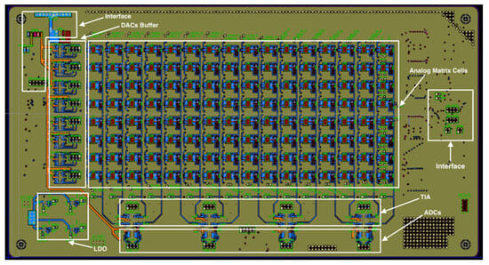
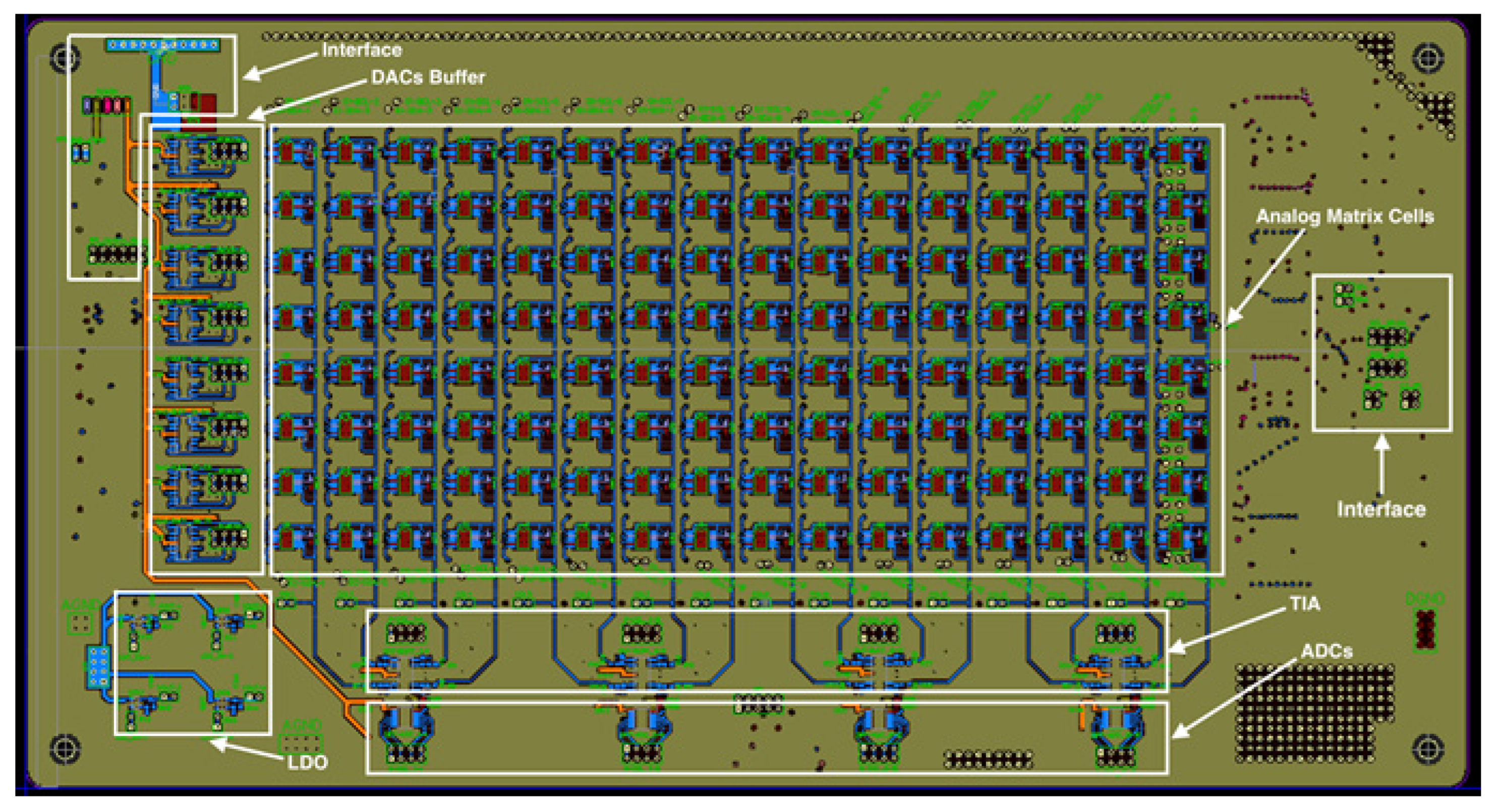
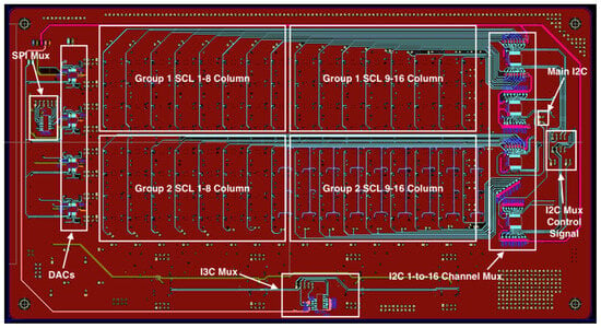
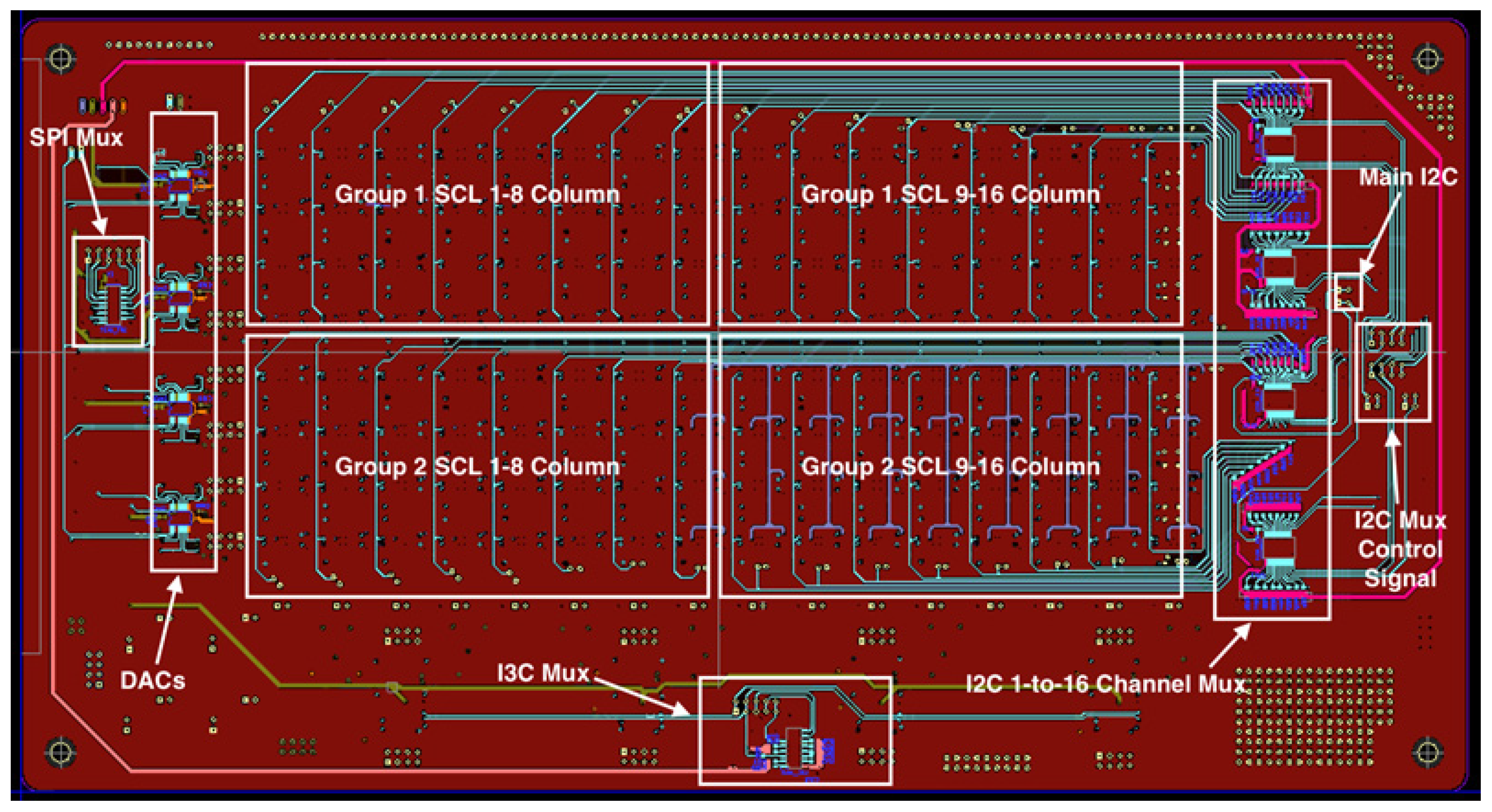
The PCB for the phase-two analog computing matrix is a large-format, high-density, 4-layer board with large-format dimensions 365 mm × 195 mm (Figure 10 and Figure 11).
Figure 10.
Top Layer of PCB Layout. Components and their positions marked in white.
Figure 11.
Bottom Layer of PCB Layout. Components and their positions marked in white.
4.2. Measurements
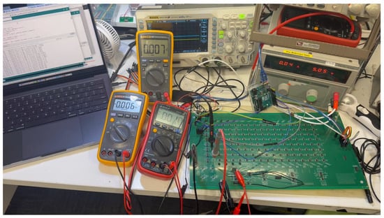
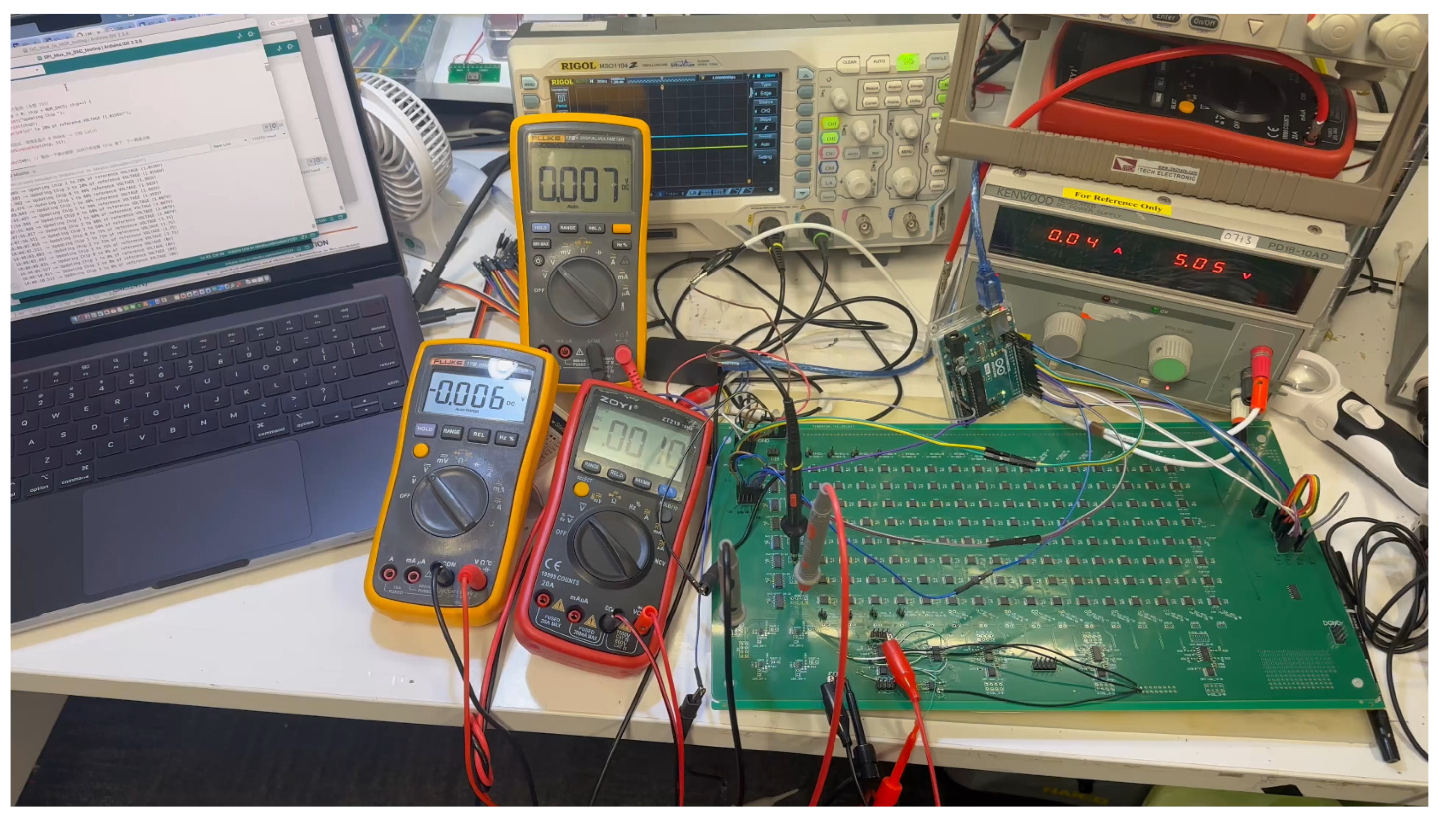
An experimental setup was used to test and verify the AMC theory by measuring the system’s actual output (Figure 12) and comparing it with the expected result. Three distinct tests were conducted to evaluate different parameters at various phases of the system.
Figure 12.
Experimental set-up.
4.2.1. TIA and Inverting Op-Amp Output After Current Summation
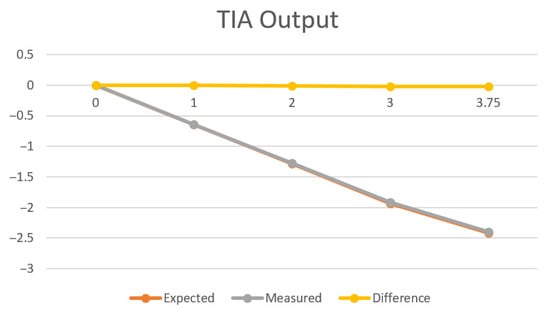
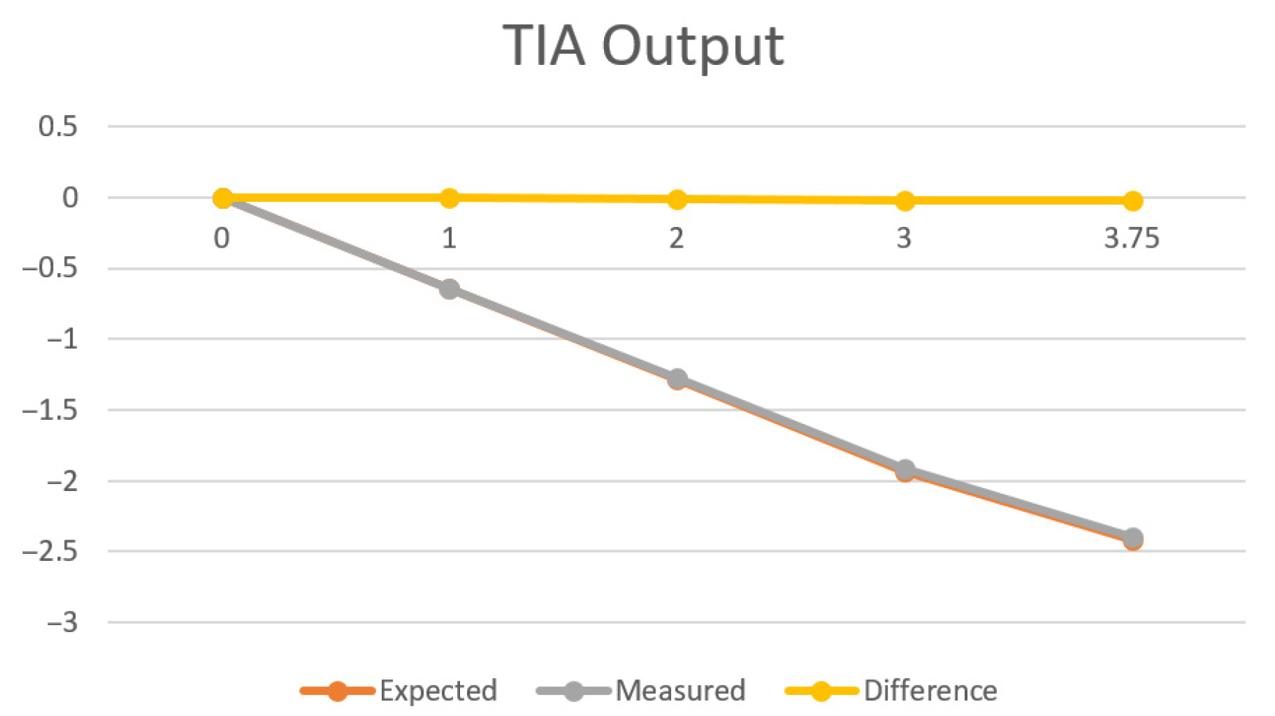
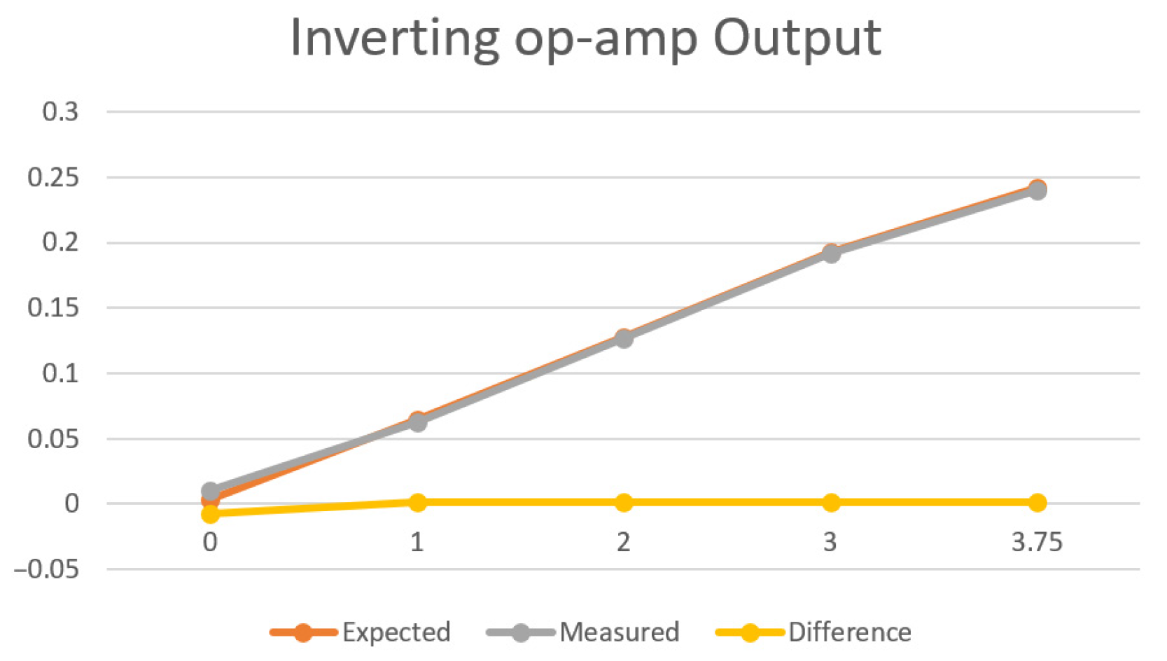
To validate the analog core, all cells in a column were programmed to 50 kΩ (Figure 13). The transimpedance amplifier (TIA) used 1 kΩ feedback (1000× gain), followed by a 0.1× inverting amplifier.
Figure 13.
TIA.
Table 3 shows that the DACs, ADCs, resistors, TIAs and inverting op-amps are functioning as intended. The results indicate a negligible difference across the entire DAC input range.
Table 3.
Comparison between expected and measured TIA and inverting op-amp outputs after current summation.
4.2.2. TIA Output of Single Channel in a Cell
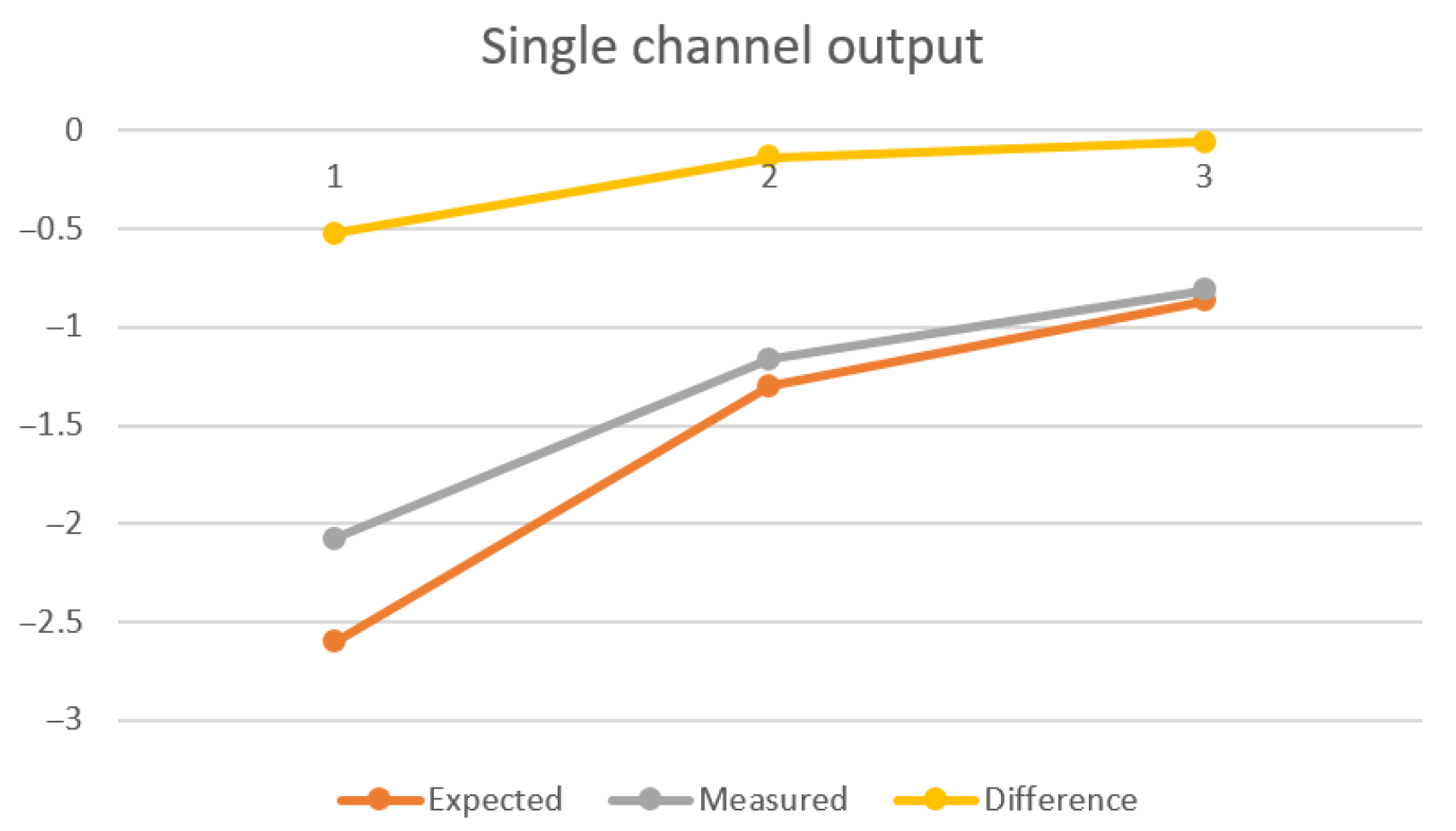
(Figure 14) Individual cell characterization was performed by applying a fixed input voltage Vin to a single channel while sweeping the programmable resistance of an MCP4552 digital potentiometer (100 kΩ end-to-end, 257 steps). This test verifies single-cell functionality and quantifies the parasitic contribution of interconnect resistance (Table 4). The expected TIA output, derived from the programmed wiper position, follows the relation given below.
Expected TIA output = Vin × (1/(100K × (step/256)) × (−1000))
Figure 14.
Inverting op-amp.
Table 4.
Comparison between expected and measured output voltage of TIA output of single channel in a cell across resistance steps.
The largest deviations occur at extreme resistance settings (near 0 Ω and 100 kΩ), as anticipated. Errors decrease markedly with intermediate wiper positions. Under typical inference workloads, where conductance values follow an approximately normal distribution, the impact of these edge-case nonlinearities is expected to be negligible.
4.2.3. Analog Mapping on ADC Output
(Figure 15) A comprehensive end-to-end validation was performed to verify that the analog matrix output reconstructs the same dot-product result as an ideal digital computation. By evaluating the full signal chain (DAC → matrix conductance → current summation → TIA/inverting amplifier → ADC → digital reconstruction), this test serves as the final correctness check for the proposed digital-analog-digital mapping flow.
Figure 15.
Single channel.
Based on the mapping derived in Section 3.3 and restated in Equation (16), the ADC code is proportional to the digital dot-product term (DDAC⋯F) up to a fixed scale factor determined by the DAC/ADC references, resolutions, and the output gain network. In firmware, the reconstructed digital result is obtained by applying a single calibration gain:
where DADC is the raw ADC reading and k is a constant scaling factor. The characterization comprised two complementary tests:
- Test A: fixed DAC input voltage with varying conductance values;
- Test B: fixed conductance with varying DAC input voltages.
- Test A: fixed DAC input, varying conductance
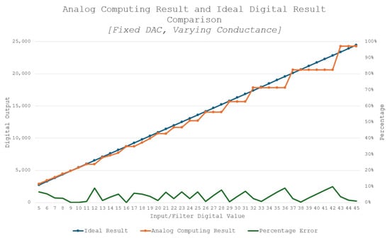
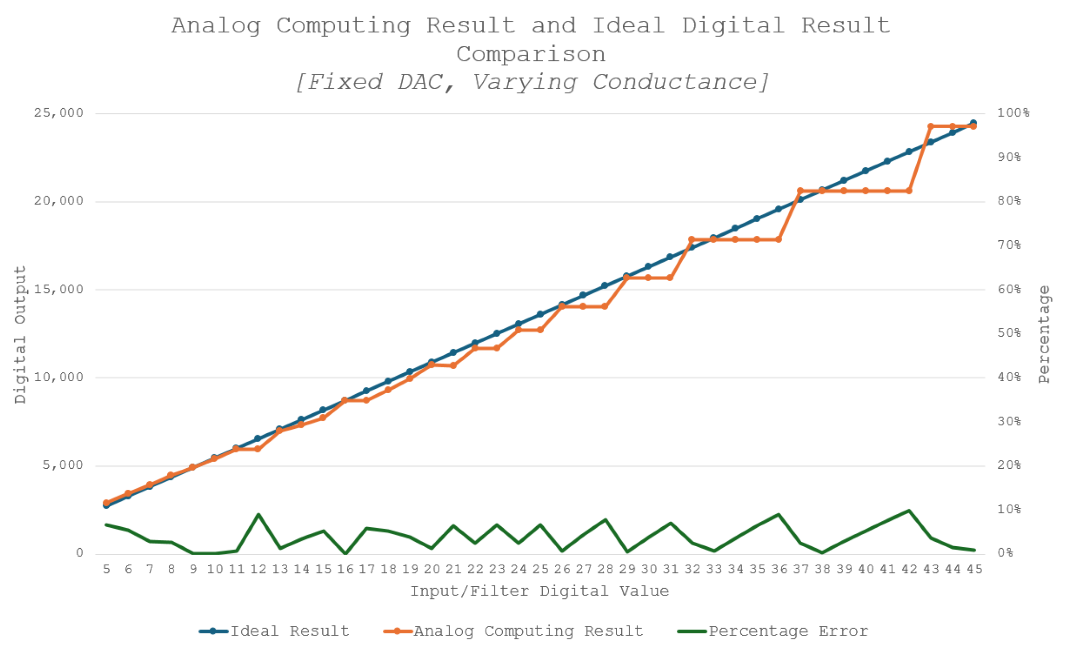
In the first sweep, the DAC input was held constant while the conductance (mapped weight) was swept across the available operating range. For each point, the ideal digital sum and reconstructed result were computed. Figure 16 compares the reconstructed analog results against the ideal digital values and plots the corresponding percentage error.
Figure 16.
Analog computing result and ideal digital result comparison varying conductance.
Across the mid-range operating region, the reconstruction tracked the ideal result with a mean absolute percentage error (MAPE) of approximately 3.8% and a worst-case error below 9%. Larger relative errors are observed at very small outputs (low codes), where fixed offsets and quantization represent a higher fraction of the signal. At the high end of the sweep, the output begins to compress due to limited analog headroom (TIA/output stage and ADC input range), producing a gradual increase in error as the ADC code approaches saturation.
- Test B: fixed conductance, varying DAC input
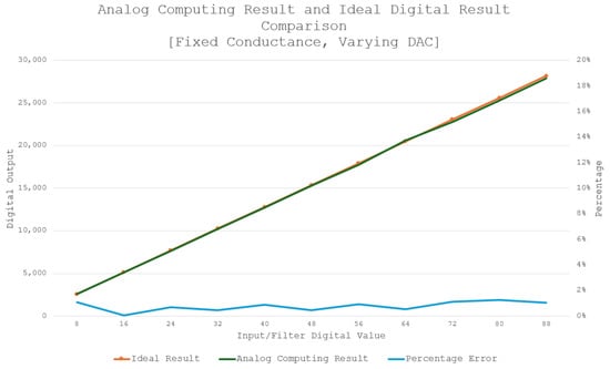
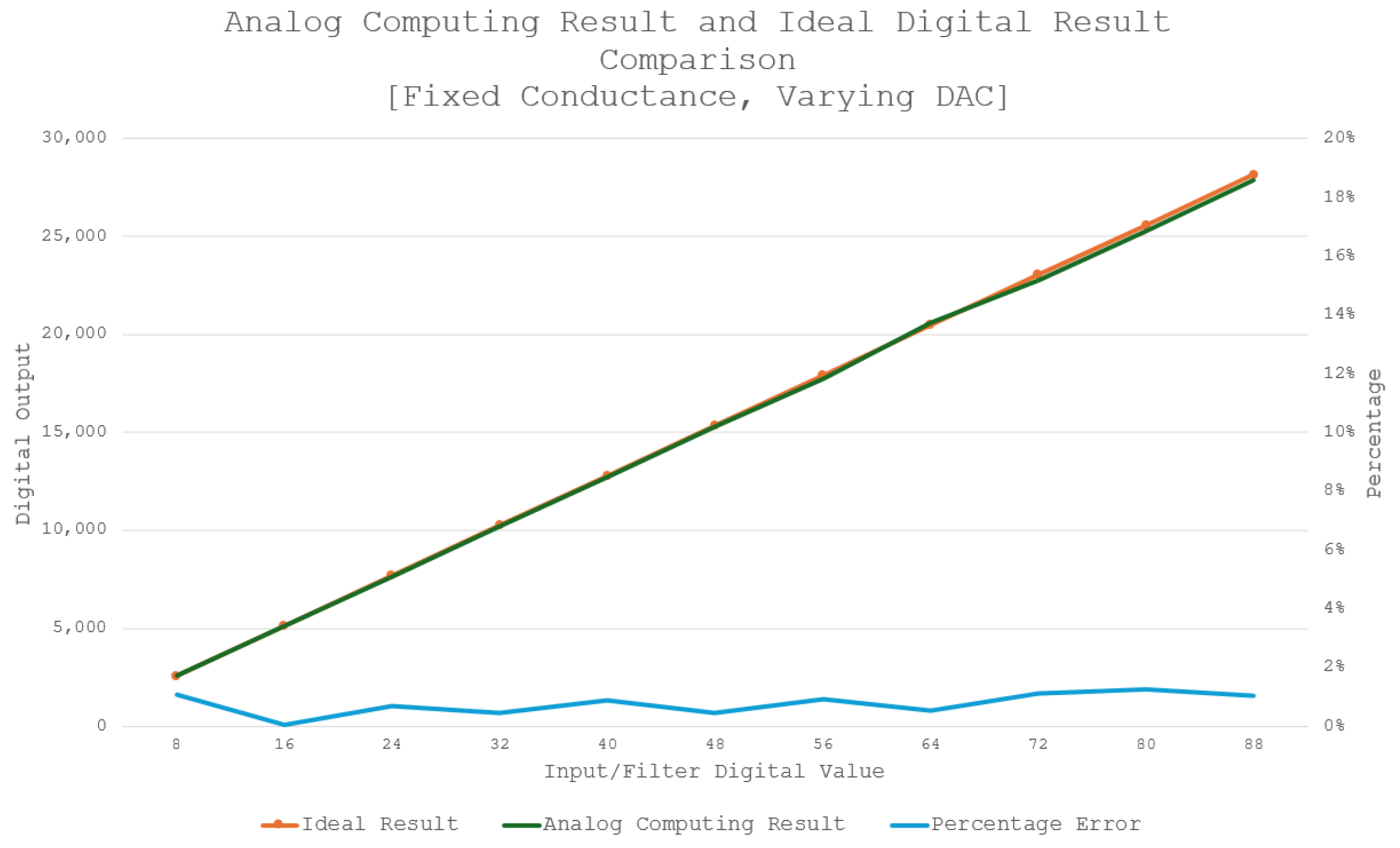
In the second sweep, the conductance code was held constant (corresponding to a fixed mapped weight) while the DAC input code was swept. The ideal digital sum and reconstructed result were computed in the same manner as Test A. Figure 17 shows that the reconstructed results closely match the ideal digital values over the central region of the DAC range. For DAC codes 16 to 88, the MAPE is approximately 0.74% with a worst-case error below 1.3%, demonstrating that the mapping and firmware reconstruction are consistent when the analog signal remains within the linear input/output range. Similar to Test A, the smallest DAC code exhibits a higher percentage error due to quantization and offset dominance. Additionally, the largest DAC codes exhibit rising error caused by output compression near the circuit swing limits.
Figure 17.
Analog computing result and ideal digital result comparison varying DAC conductance.
Overall, the end-to-end measurements confirm that the proposed domain-mapping and reconstruction pipeline is correctly implemented and produces digitally usable outputs for neural-network inference, provided that the operating point avoids the extreme low-signal regime and the high-saturation regime. These constraints can be satisfied in practice by standard per-layer scaling/normalization and by selecting appropriate TIA gain and ADC input range for the expected activation and weight statistics.
4.2.4. Power Consumption
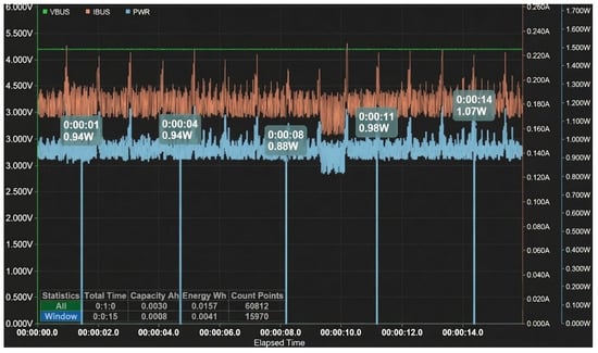
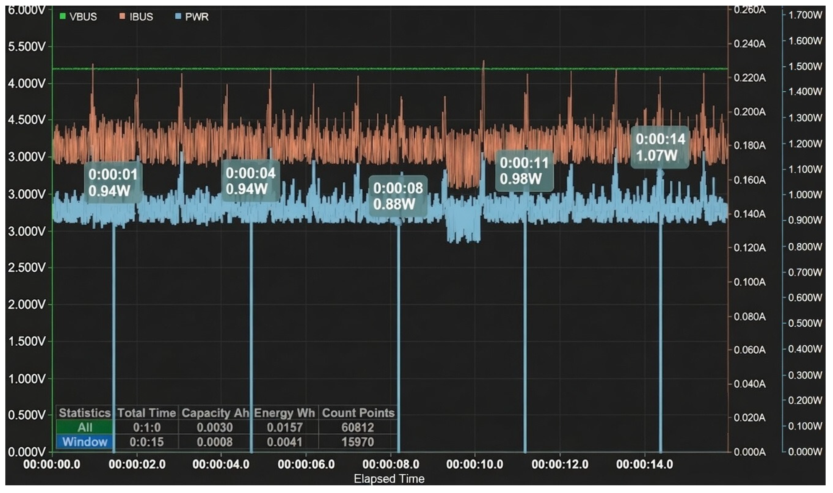
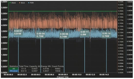
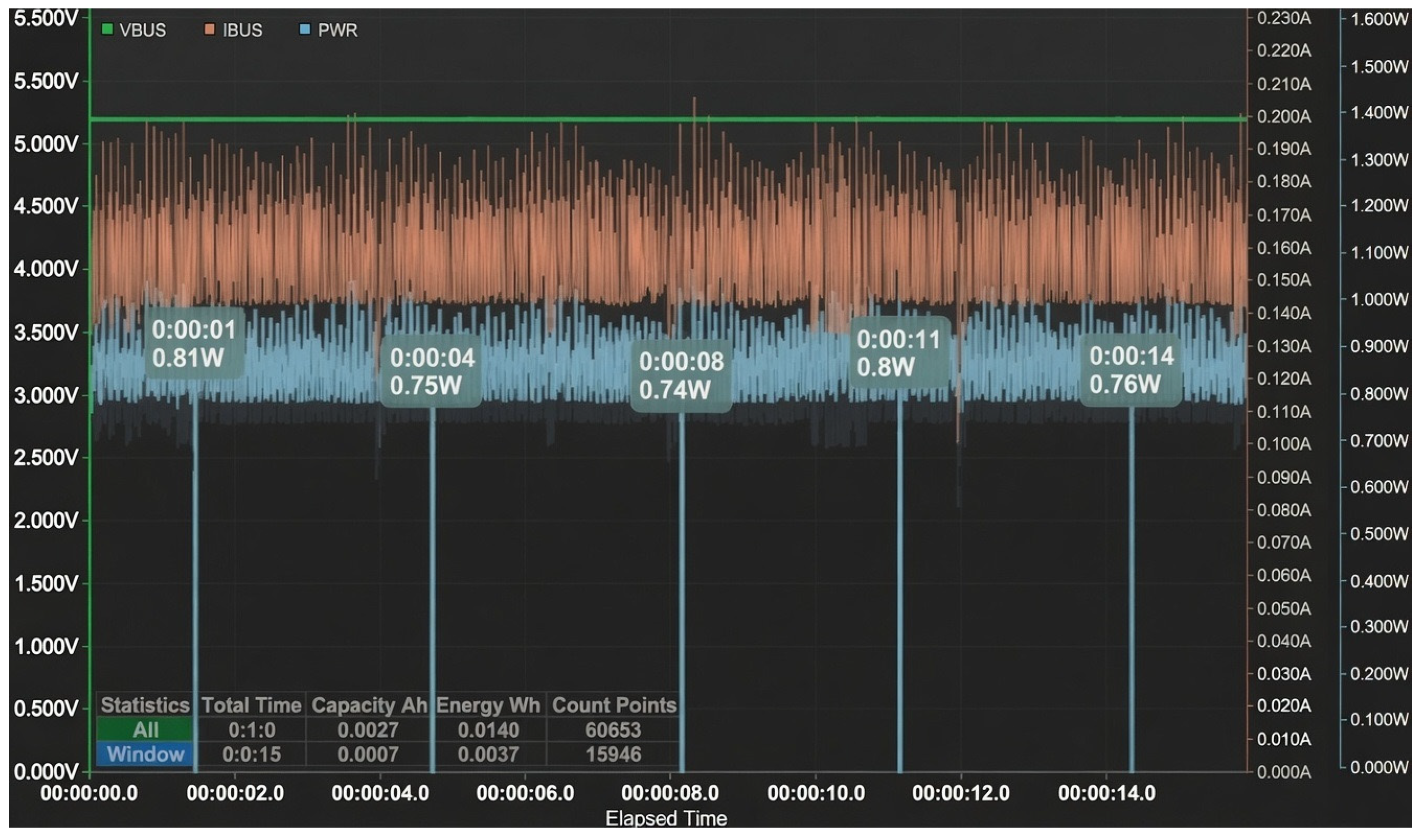
Figure 18 and Figure 19 illustrate the power consumption of the proposed setup for both scenarios. The average power consumption with the analog crossbar board ranges from 0.8 W to 1.1 W, compared to 0.7 W to 0.95 W without it. While the board slightly increases total power usage, a significant portion of this energy is dissipated during off-board data transmission. This overhead, which is a primary limitation of the current experimental prototype, obscures the power reductions achieved by the analog computing array. These losses will be substantially alleviated once the architecture is implemented at the silicon level. Furthermore, as the current prototype maps only a single layer type, the architecture’s full efficiency potential will be realized when multiple layers are executed directly in analog hardware.
Figure 18.
Power consumption with offload.
Figure 19.
Power consumption without offload.
4.2.5. Pointwise Layer Inference Time
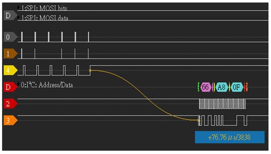
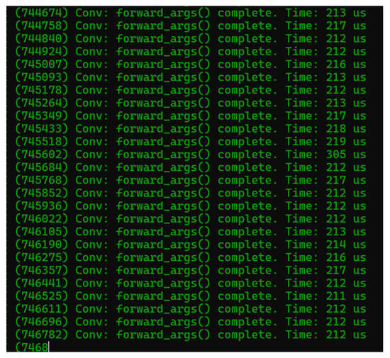
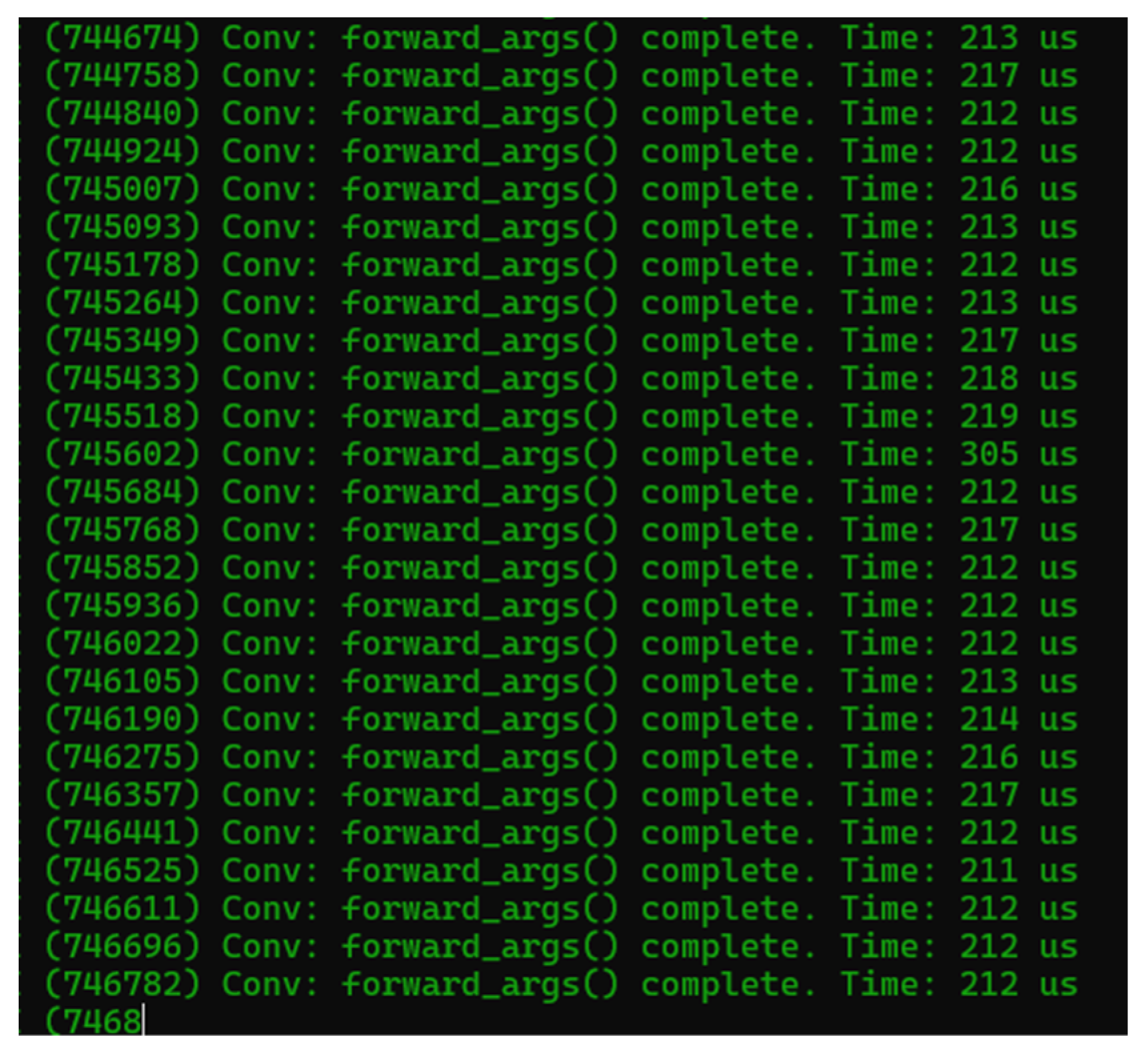
Figure 20 and Figure 21 display the inference times for the pointwise layer on the analog crossbar array and the ESP32-P4, respectively. The crossbar array measurement (Figure 20) was captured using a DSLogic logic analyzer, while the ESP32-P4 result was obtained via the native Espressif platform. The analog crossbar array achieves an inference time of approximately 76 µs, roughly one-third of the 215 µs required by the ESP32-P4. These results demonstrate that, despite its bulky prototype form factor, the analog crossbar array outperforms the ESP32-P4’s on-chip digital inference. This validates the effectiveness of analog crossbar acceleration for neural network inference, with even greater performance gains expected upon silicon-level implementation.
Figure 20.
Pointwise layer inference time on crossbar array.
Figure 21.
Pointwise layer inference time on ESP32-P4.
4.2.6. Overhead and Latency on Cross Array
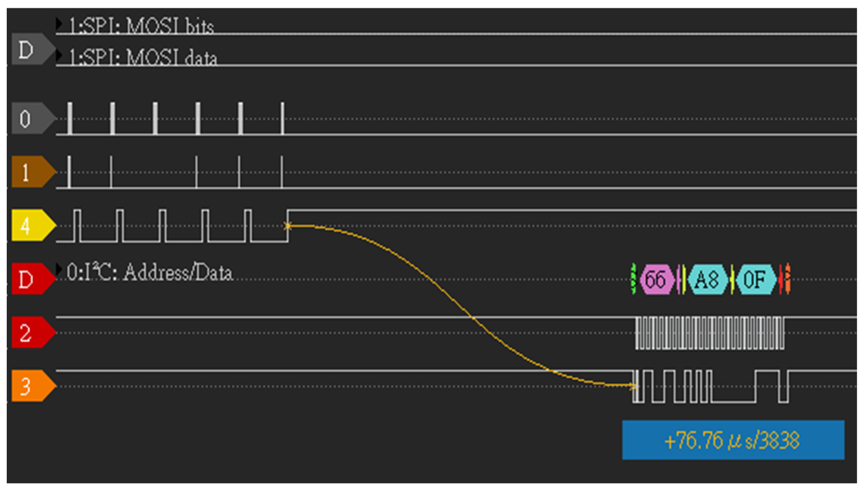
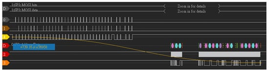
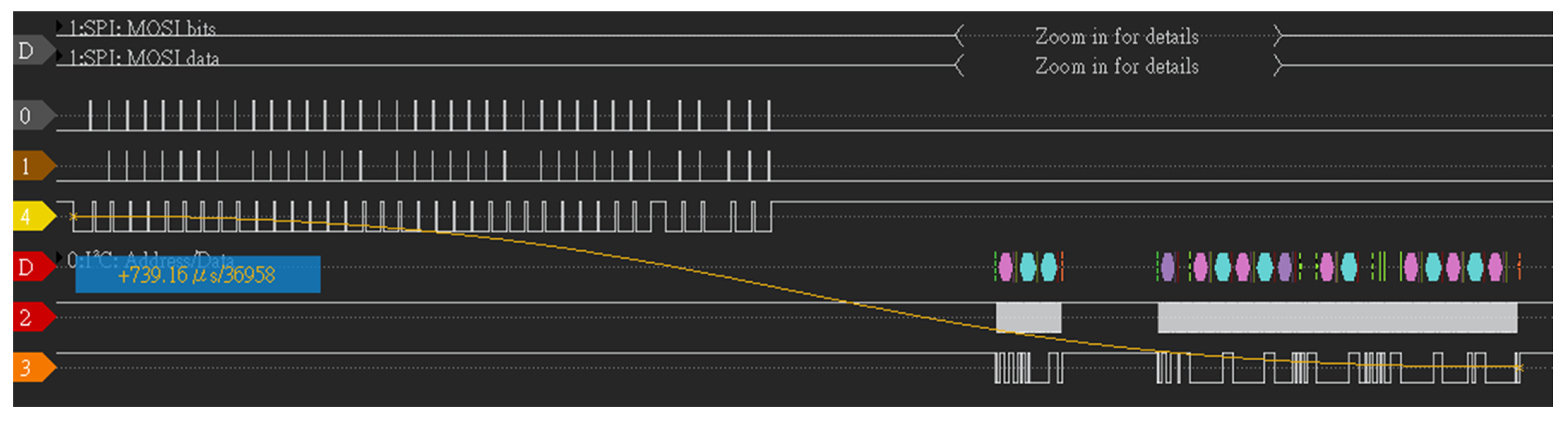
Although the analog crossbar array achieves inference for the pointwise layer approximately three times faster (76 µs) than the on-chip digital implementation on the ESP32-P4 (215 µs), it incurs substantial overhead from DAC settling and ADC conversion. As shown in Figure 22, the total processing time-from writing input values to the AD5308ARUZ DAC via SPI to completing the MAX11614EEE ADC conversion via I2C is approximately 739.16 µs. The core analog inference time (76 µs) appears as a gap between the two waveform blocks, resulting in an overhead of 663.16 µs (more than 7.7 times the actual computation time). Consequently, the overall latency in the current prototype exceeds that of running the layer solely on the ESP32-P4. This limitation stems primarily from off-chip data conversion and communication overheads, which are expected to be significantly reduced when the architecture is implemented on a single silicon die.
Figure 22.
Pointwise Layer Inference Time with DACs and ADCs overhead on Crossbar Array.
4.3. People Detection
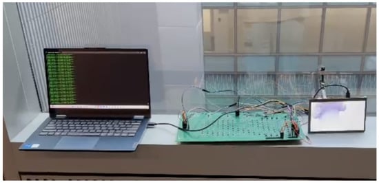
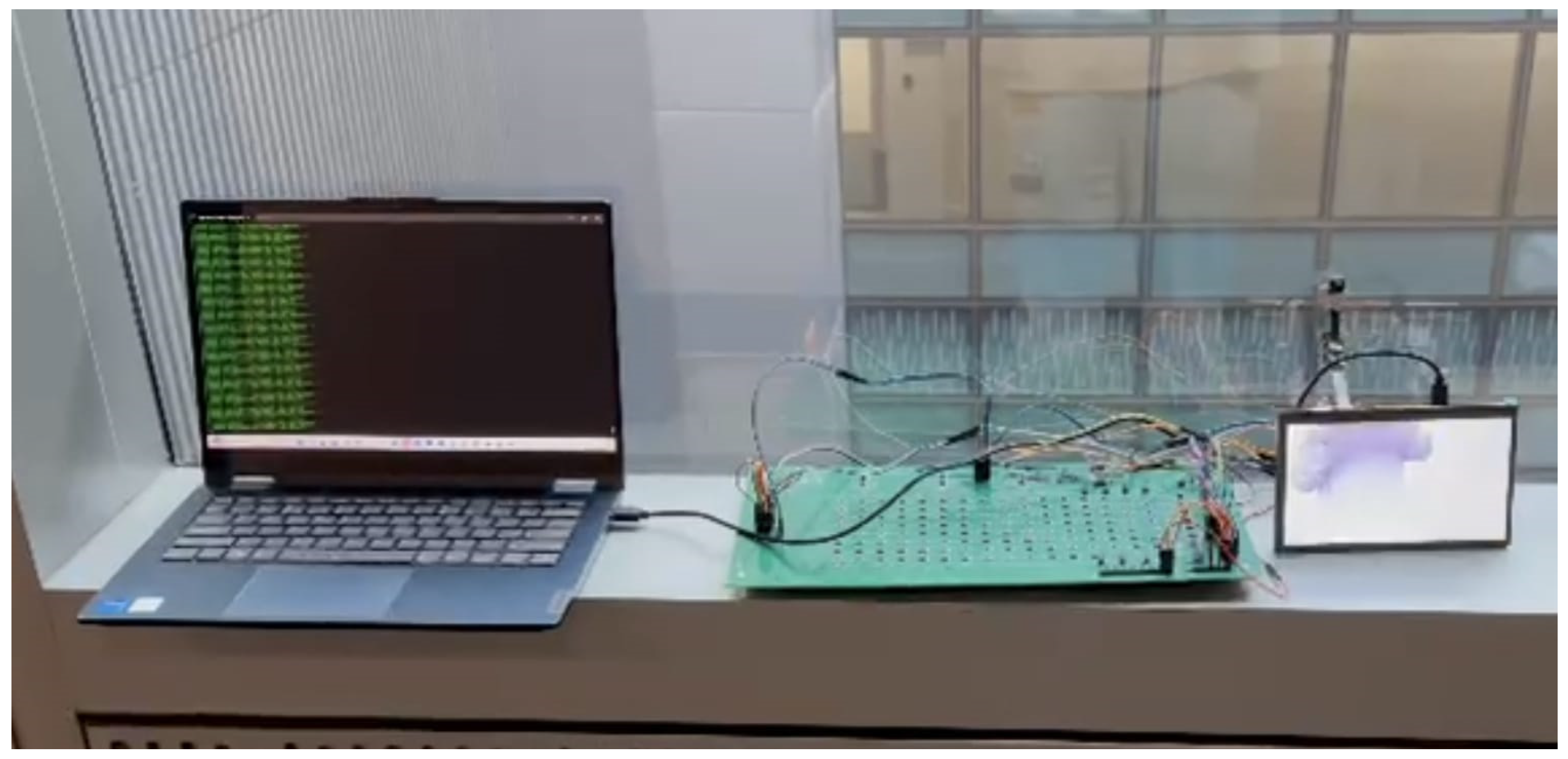
To demonstrate the feasibility of the whole system, the complete inference pipeline (Figure 5) was executed on the integrated platform shown in Figure 23. A laptop served solely as the power source and debug console of the setup. Meanwhile, the ESP32-P4 acted as the digital host, performing image acquisition and preprocessing, orchestrating weight programming, streaming inputs to the analog matrix, and executing the remaining non-accelerated layers in the digital domain. One target pointwise-convolution/MVM layer was offloaded to the analog computing matrix, with the equation as: Target = Input(x) × filter(f). By substituting the pointwise-convolution equation into Equation (8) and mapping the filter into range of [0, 255], Equation (18) was obtained:
Figure 23.
People Detection Setup.
The resulting current was converted into a voltage via the TIA as follows:
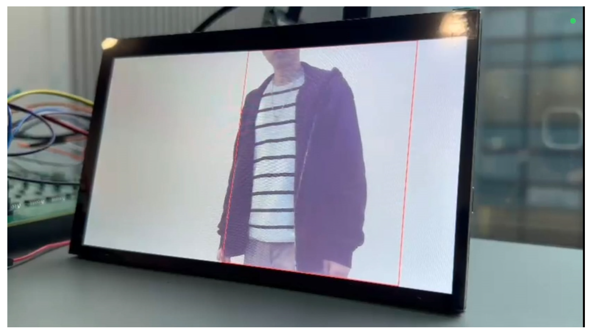
Detection results were displayed on a portable screen with overlaid bounding boxes indicating successful identification. During live operation, the system delivered robust performance and high detection accuracy, even in multi-person scenes. Although the current architecture experiences a data transmission bottleneck that introduces measurable overheads (as detailed in the previous section), it still achieves continuous, real-time processing through its low-power, mixed-signal differential computing network. Implementing this architecture at the silicon circuit level will minimize data transmission bottlenecks and drastically reduce hardware latency, thereby yielding significantly stronger performance. Figure 24 illustrates a representative real-time run, showing a bounding box correctly drawn around a detected person.
Figure 24.
People Detection result.
5. Conclusions
This study validates a reconfigurable analog matrix integrated with a RISC-V microcontroller for energy-efficient edge AI. By performing MVM in the analog domain, the hybrid design bypasses the von Neumann bottleneck to achieve O(1) time complexity. The 32 × 16 differential crossbar is programmed via I2C and interfaced via SPI, enabling real-time processing for AIoT, robotics, and electric vehicle applications. Experimental measurements demonstrate a TIA/inverting op-amp error of less than 2%, closely aligning with ideal models across various DAC inputs and resistance steps. Furthermore, successful on-device people detection demonstrates reliable analog computing with bounded error. The I2C-programmable cells provide high reconfigurability, offering a practical pathway toward low-power, real-time edge intelligence. Future work will focus on scaling to larger arrays (e.g., 128 × 128), incorporating switched-capacitor operation, and implementing advanced noise calibration techniques.
Author Contributions
Conceptualization, D.N. and K.H.L.; methodology, W.C.L.; formal analysis, W.C.L. and S.C. (Sunny Chan).; writing—original draft preparation, W.C.L., M.M., H.W. and S.W.; writing—review and editing, all authors. All authors have read and agreed to the published version of the manuscript.
Funding
This research received no external funding.
Institutional Review Board Statement
Not applicable.
Informed Consent Statement
Not applicable.
Data Availability Statement
The original contributions presented in this study are included in the article. Further inquiries can be directed to the corresponding authors.
Conflicts of Interest
Author David Ng serves as CEO of High Tech Technology Co., Ltd. and FinSiliconX Limited. Authors Chi Hong Chan, Roy Ng, Hugo Wong, Steve Chim, Patrick Chang, and Steven Wong were employed by High Tech Technology Co., Ltd. Authors Sunny Chan and Matt Mak were employed by FinSiliconX Limited. Raymond Chik is the founder of DRC Enterprises. Author Wen Chin Lo conducted experiments utilizing laboratory equipment provided by High Tech Technology Co., Ltd. The remaining authors declare that the research was conducted in the absence of any commercial or financial relationships that could be construed as a potential conflict of interest.
References
- Mak, M.; Lam, K.H.; Ng, D.; Lo, C.; Chen, J.; Chang, P.; Ng, R.; Mui, J.; Chim, S.; Bu, S. Optimized multi-phase buck converter with dynamic current-balancing for low-voltage high-current EV-CPU applications. In Proceedings of the International Council on Electrical Engineering Conference 2024 (ICEE 2024), Kitakyushu, Japan, 30 June–4 July 2024. [Google Scholar]
- Bourechak, A.; Zedadra, O.; Kouahla, M.N.; Guerrieri, A.; Seridi, H.; Fortino, G. At the confluence of artificial intelligence and edge computing in IoT-based applications: A review and new perspectives. Sensors 2023, 23, 1639. [Google Scholar] [CrossRef] [Scilit] [PubMed]
- He, X.H.; Ng, D.; Lam, K.H.; Chan, C.H.; Ng, R.; Mak, M.; Chim, S. Analog in-memory neuron array computing for power-constrained edge CNN applications. In Proceedings of the 13th IET International Conference on Advances in Power System Control, Operation and Management (APSCOM 2025), Hong Kong, China, 9–12 November 2025. [Google Scholar]
- Shuvo, M.M.H.; Islam, S.K.; Cheng, J.; Morshed, B.I. Efficient acceleration of deep learning inference on resource-constrained edge devices: A review. Proc. IEEE 2023, 111, 42–91. [Google Scholar] [CrossRef] [Scilit]
- Cheng, J.; Zhou, H.; Dong, J. Photonic matrix computing: From fundamentals to applications. Nanomaterials 2021, 11, 1683. [Google Scholar] [CrossRef] [Scilit] [PubMed]
- Xue, C.X.; Chiu, Y.C.; Liu, T.W.; Huang, T.Y.; Liu, J.S.; Chang, T.W.; Kao, H.Y.; Wang, J.H.; Wei, S.Y.; Lee, C.Y.; et al. A CMOS-integrated compute-in-memory macro based on resistive random-access memory for AI edge devices. Nat. Electron. 2021, 4, 81–90. [Google Scholar] [CrossRef] [Scilit]
- Li, E.; Zeng, L.; Zhou, Z.; Chen, X. Edge AI: On-demand accelerating deep neural network inference via edge computing. IEEE Trans. Wirel. Commun. 2020, 19, 447–457. [Google Scholar] [CrossRef] [Scilit]
- Letaief, K.B.; Shi, Y.; Lu, J.; Lu, J. Edge artificial intelligence for 6G: Vision, enabling technologies, and applications. IEEE J. Sel. Areas Commun. 2022, 40, 5–36. [Google Scholar] [CrossRef] [Scilit]
- Jia, L.; Zhou, Z.; Xu, F.; Jin, H. Cost-efficient continuous edge learning for artificial intelligence of things. IEEE Internet Things J. 2022, 9, 7325–7337. [Google Scholar] [CrossRef] [Scilit]
- Wan, W.; Kubendran, R.; Schaefer, C.; Eryilmaz, S.B.; Zhang, W.; Wu, D.; Deiss, S.; Raina, P.; Qian, H.; Gao, B.; et al. A compute-in-memory chip based on resistive random-access memory. Nature 2022, 608, 504–512. [Google Scholar] [CrossRef] [Scilit] [PubMed]
- Ansari, M.S.; Cockburn, B.F.; Han, J. An improved logarithmic multiplier for energy-efficient neural computing. IEEE Trans. Comput. 2021, 70, 614–625. [Google Scholar] [CrossRef] [Scilit]
- Napoli, E.; Strollo, A.G.M.; Zacharelos, E.; Di Meo, G. Comprehensive analysis of input order invariant approximate 4-2 compressors for binary multipliers. In Proceedings of the 2024 IEEE International Symposium on Circuits and Systems (ISCAS), Singapore, 19–22 May 2024. [Google Scholar] [CrossRef] [Scilit]
- Hérissé, K.; Larras, B.; Stefanelli, B.; Kaiser, A.; Frappé, A. An incremental time-domain mixed-signal matrix-vector-multiplication technique for low-power edge-ai. IEEE Trans. Circuits Syst. I Regul. Pap. 2024, 71, 6470–6481. [Google Scholar] [CrossRef] [Scilit]
- Wang, W.C.; Zhang, S.; Shamieh, L.; Kidambi, N.V.; Chakraborty, I.; Mukhopadhyay, S. MIX-ACIM: A 28nm mixed-precision analog Compute-in-Memory with digital teature restoration for vector-matrix multiplication. IEEE Solid-State Circuits Lett. 2025, 8, 213–216. [Google Scholar] [CrossRef] [Scilit]
- Waterman, A. Design of the RISC-V Instruction Set Architecture. Ph.D. Dissertation, UC Berkeley, Berkeley, CA, USA, 2016; p. 32. [Google Scholar]
- Anisha, S. RISC-V International. In RISC-V 2024: A Year of Global Growth and Innovation; RISC-V: Zurich, Switzerland, 2024; Available online: https://riscv.org/blog/risc-v-2024-a-year-of-global-growth-and-innovation/ (accessed on 22 April 2026).
- Alspector, J.; Gupta, B.; Allen, R.B. Performance of a stochastic learning microchip. In Advances in Neural Information Processing Systems (NIPS 1988); MIT Press: Cambridge, MA, USA, 1988; Volume 1, pp. 748–760. [Google Scholar]
- Li, J.; Xue, Y.; Li, Y.; Jia, H.; Zhou, Z.; Yang, L.; Ren, S.; Chen, J.; He, Y.; Xue, K.; et al. Fully analog iteration for solving matrix equations with in-memory computing. Sci. Adv. 2025, 11, eadr6391. [Google Scholar] [CrossRef] [Scilit] [PubMed]
- Ielmini, D.; Wong, H.-S.P. In-memory computing with resistive switching devices. Nat. Electron. 2018, 1, 333–343. [Google Scholar] [CrossRef] [Scilit]
- Zuo, P.; Wang, Q.; Luo, Y.; Xie, R.; Wang, S.; Cheng, Z.; Bao, L.; Wang, Z.; Cai, Y.; Huang, R.; et al. Precise and scalable analogue matrix equation solving using resistive random-access memory chips. Nat. Electron. 2025, 8, 1222–1233. [Google Scholar] [CrossRef] [Scilit]


Disclaimer/Publisher’s Note: The statements, opinions and data contained in all publications are solely those of the individual author(s) and contributor(s) and not of MDPI and/or the editor(s). MDPI and/or the editor(s) disclaim responsibility for any injury to people or property resulting from any ideas, methods, instructions or products referred to in the content. |
© 2026 by the authors. Licensee MDPI, Basel, Switzerland. This article is an open access article distributed under the terms and conditions of the Creative Commons Attribution (CC BY) license.