


Abstract
Copper selenide (Cu2Se), as a typical p-type narrow bandgap semiconductor, has garnered significant attention in the fields of thermoelectrics and optoelectronics due to its inherent low thermal conductivity, high Seebeck coefficient, low cost, and environmental friendliness. Compared with bulk materials, Cu2Se thin films exhibit unique advantages in microdevice integration and flexible applications, holding great potential for applications in flexible thermoelectric generators, solar cells, and photodetectors. This article systematically reviews the research progress of Cu2Se thin films, focusing on key preparation parameters such as growth temperature, annealing conditions, copper/selenium element ratio, and substrate type, and elucidates their regulation of film microstructure, crystal phase structure, and thermoelectric/optoelectronic properties. It delves into the mechanisms of doping strategies such as carrier concentration regulation, band engineering, and defect modification, clarifying the synergistic optimization effects of different doping elements on conductivity, Seebeck coefficient, and thermal conductivity. The article summarizes the current application status of Cu2Se thin films, points out existing challenges such as poor process reproducibility and insufficient thermal stability, and anticipates future research directions such as multi-parameter synergistic optimization and heterojunction design, providing a systematic reference for the development and practical application of high-performance Cu2Se-based functional thin films.
1. Introduction
Thermoelectric (TE) devices can convert heat into electricity and also achieve the reverse conversion from electricity to heat. They are used in many applications, such as temperature sensors and industrial waste heat recovery. Generally, a higher ZT value of a thermoelectric material (ZT = S2σT/κ, where S is the Seebeck coefficient, σ is the electrical conductivity, T is the absolute temperature, and κ is the thermal conductivity) means better thermoelectric performance and higher device efficiency. Today, most commercial TE devices use toxic and expensive tellurium-based alloys, which is a major challenge for the development of TE devices. It is still very important to study new thermoelectric materials that have a high power factor (PF = S2σ), low cost, and no toxicity, as well as materials with low thermal conductivity.
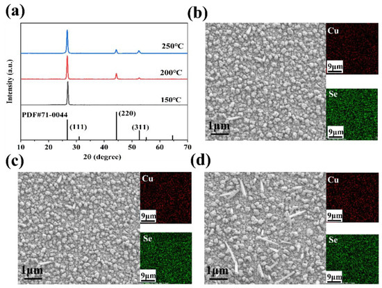
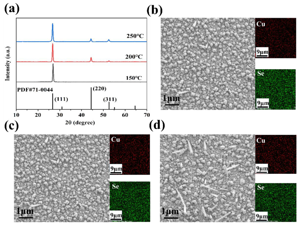
Cu2Se has low intrinsic thermal conductivity and a high Seebeck coefficient, making it a promising potential candidate to replace traditional tellurium-based materials. Yang et al. reported that bulk Cu2Se can reach a ZT value of about 2.5, which is one of the highest values among thermoelectric materials [1]. At present, most research on Cu2Se focuses on bulk materials. Compared with three-dimensional bulk materials, two-dimensional thin films are more compatible with modern semiconductor technology and offer unique advantages for building and applying thermoelectric micro/nano devices. Meanwhile, Yadav et al. reported that Cu2Se thin films show a good polycrystalline structure and uniform nanoscale morphology [2], with a pure composition free of impurities. Figure 1 shows the XRD patterns and surface morphology of Cu2Se thin films at different temperatures. These thin films have suitable transparency from the visible to the near-infrared region, an optical bandgap that matches the visible light response, and excellent key optical parameters such as refractive index and dielectric constant.
Figure 1.
(a) X-ray diffraction (XRD) and (b–d) SEM images of the Cu2Se-based thin films deposited at 150 °C, 200 °C, and 250 °C [3].
In terms of applications, Cu2Se thin films have become important candidate materials in the field of flexible thermoelectric energy harvesting due to their intrinsic superionic conducting properties, low thermal conductivity, and environmental friendliness. By optimizing the Cu/Se stoichiometric ratio, Huang et al. achieved a high power factor and ZT value at room temperature [4]. The films also maintained stable output power after many bending cycles, showing excellent mechanical flexibility and thermoelectric stability. Cu2Se thin films with controllable orientation, prepared by pulsed laser deposition (PLD), further improved the power factor through the synergistic effect between carrier concentration and Seebeck coefficient. These films can be used in high-performance flexible thermoelectric devices [5]. For scalable fabrication, flexible Cu2Se thin films prepared by a spin-coating process using a true solution precursor ink showed excellent thermoelectric performance at high temperatures. Their performance hardly degraded after a thousand bending cycles, laying the foundation for low-cost, large-area industrial production of flexible thermoelectric devices [6].
In the field of optoelectronic applications, Cu2−xSe thin films are widely used in solar cell heterostructures because of their excellent photoelectric conversion properties. For example, Cu2−xSe-n-Si heterojunction devices can achieve high photoelectric conversion efficiency. Cu2Se thin films can serve as hole injection layers for p-type organic semiconductors, effectively improving the carrier injection efficiency of organic optoelectronic devices [7]. Recent studies have further expanded the applications of Cu2Se thin films in the fields of photodetection and photocatalysis. By controlling the morphology and composition of the films, their light absorption properties and carrier separation efficiency are optimized. This provides important references for developing new optoelectronic devices and energy conversion materials [8].
Therefore, this paper selects Cu2Se material as the research object and systematically and comprehensively reviews the thermoelectric and optoelectronic properties of Cu2Se thin films obtained through different preparation processes. This is to fully understand the current research status and progress of Cu2Se thin films and to provide references and directions for future research.
2. Properties of Cu2Se
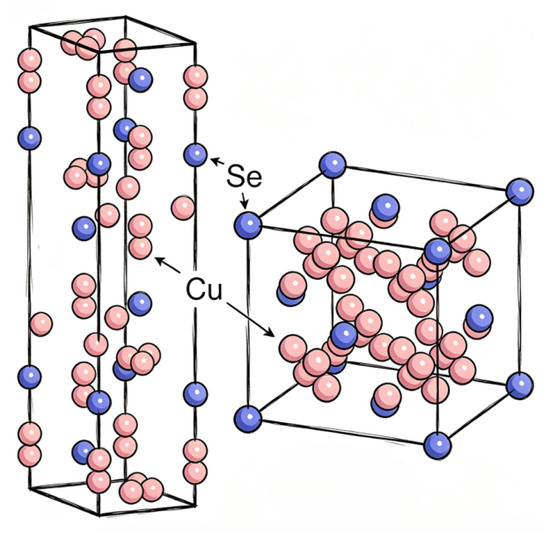
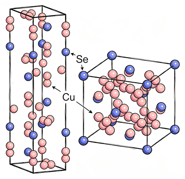
Cu2Se is an intrinsic p-type narrow-bandgap semiconductor material. Its holes mainly come from Cu vacancies. Cu2Se has two crystal structures. At room temperature, it exists in the α phase (monoclinic system). At high temperatures, it exists in the β phase (cubic system), as shown in Table 1. The lattice constants of the α phase are a = 7.05 Å, b = 20.481 Å, and c = 4.145 Å. When the temperature exceeds about 400 K, the crystal structure undergoes a phase transition from the monoclinic α phase to the cubic β phase. The lattice constants of the β phase are a = b = c = 5.787 Å. Both the α and β phases use the Se atoms to form a face-centered cubic sublattice as the framework, with Cu atoms distributed within it. In the α phase, Cu atoms are fully distributed in the tetrahedral interstitial positions. In the β phase, disordered Cu ions are distributed in either tetrahedral or triangular interstitial positions [9]. The positions of these Cu ions, which have a “liquid-like” mobility, are not fixed [10]. They can scatter phonons, reduce the phonon mean free path, and achieve extremely low lattice thermal conductivity, thus improving thermoelectric performance [11]. Figure 2 shows the two crystal structures of Cu2Se.
Table 1.
Structural characteristics of Cu2Se.
Figure 2.
Crystal structures of α-Cu2Se and β-Cu2Se ((left) α-phase, and (right) β-phase) [12].
The performance of thermoelectric materials is mostly measured by the dimensionless figure of merit [13]:
Here, the symbols represent the Seebeck coefficient (S), electrical conductivity (σ), absolute temperature (T), and thermal conductivity (κ). The electrical performance part in the formula is separately called the power factor (PF).
The Seebeck coefficient is the ratio of the thermoelectric electromotive force to the temperature difference:
This coefficient can intuitively reflect the ability of thermoelectric materials to generate electromotive force.
For electrical conductivity σ, the ability of a material to conduct electric current can be described by this parameter:
In the formula, n is the carrier concentration, μ is the mobility of carriers in the material, τ0 is the relaxation time, and m* is the effective mass.
For thermal conductivity κ, both charge carriers and phonons together influence the value of this parameter.
To maximize the thermoelectric figure of merit, the essential requirements are a high absolute Seebeck coefficient, high electrical conductivity, and low thermal conductivity. A high Seebeck coefficient and high electrical conductivity indicate excellent thermoelectric conversion efficiency of the charge carriers, while low thermal conductivity indicates that the material has a strong ability to maintain a suitable temperature gradient. Currently, most studies on Cu2Se thin films report only the PF, rather than the full ZT. This is mainly because measuring the κ of thin films is technically demanding. It requires specialized techniques such as TDTR or the differential 3ω method. In addition, the results are highly sensitive to film thickness, substrate type, and interfacial quality. In contrast, the Seebeck coefficient and electrical conductivity can be measured simultaneously using the same apparatus, which makes the PF much easier to obtain. Therefore, the PF is a meaningful and widely used metric for evaluating the electrical transport performance of thermoelectric thin films.
3. Research Progress on Cu2Se Thin Films
Different processing parameters have different effects on the properties. It should be noted that the Seebeck coefficient, electrical conductivity, power factor, and other performance parameters summarized below are collected from various literature sources. These values were obtained under different experimental conditions, including variations in measurement temperature, atmosphere, substrate type, and device configuration. Therefore, direct quantitative comparison of absolute values across different studies should be made with caution. The main purpose of these tables is to illustrate general trends and orders of magnitude, rather than to provide strict numerical rankings.
3.1. Effect of Growth Temperature on Thin Film Properties
During the preparation of Cu2Se thin films, temperature plays a decisive role in the phase structure, chemical composition, grain size, and thermoelectric properties of the films, as shown in Table 2.
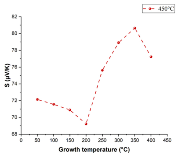
As the growth temperature increases, the grain size of the thin films usually tends to increase. At the same time, selenium, having a high saturated vapor pressure, preferentially evaporates. This leads to an increase in the Cu:Se atomic ratio and a decrease in carrier concentration in the film. These changes cause a decrease in electrical conductivity and an increase in the Seebeck coefficient, which is consistent with the basic behavior of degenerate semiconductors, Figure 3 shows the relationship between the growth temperature and the Seebeck coefficient for films grown on a glass substrate. However, an excessively high temperature causes excessive loss of selenium, leading to the precipitation of secondary phases, a decrease in hardness [14], and even disruption of the preferred orientation of the film. Therefore, there is an optimal deposition temperature window. For PLD, it is about 300 to 325 °C; for magnetron sputtering, it is about 200 °C.
Table 2.
Effect of growth temperature on thin film properties.
Figure 3.
Dependence of Seebeck coefficient on growth temperature for magnetron-sputtered Cu2Se thin films on glass [17,18].
In addition, an optimized growth temperature on a flexible substrate can also give the thin film good mechanical flexibility [14]. After hundreds of bending cycles, the resistance change is less than 5%. In summary, precise control of the deposition temperature is a key method for tuning the structural integrity, electrical transport properties, and mechanical stability of Cu2Se thin films. This has important guiding significance for the development of high-performance flexible thermoelectric devices.
3.2. Effect of Annealing Temperature on Thin Film Properties
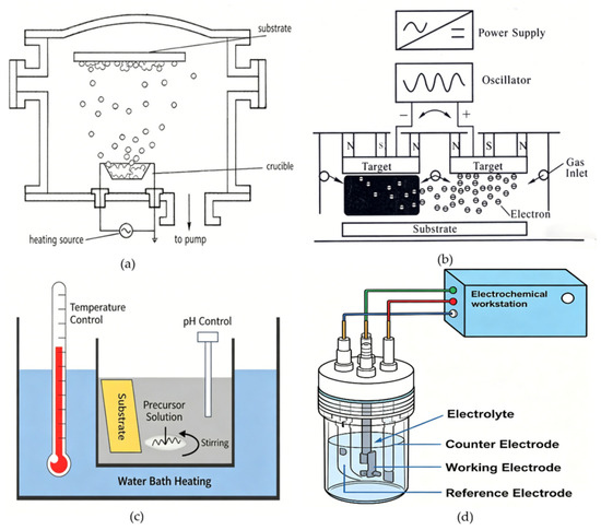
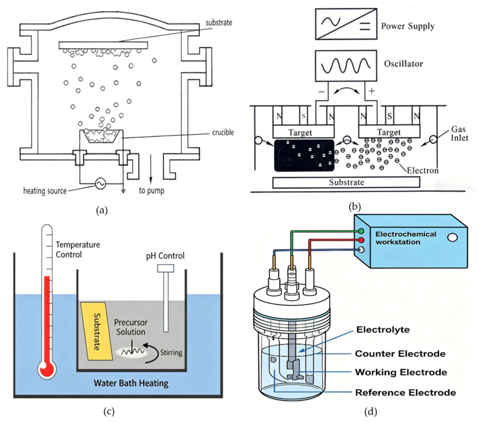
The optimization effect of annealing treatment on the properties of Cu2Se thin films strongly depends on the preparation method. Figure 4 shows different preparation methods for Cu2Se thin films, and Table 3 shows the influence of annealing temperature on the thin film properties.
Figure 4.
Different preparation methods for Cu2Se thin films: (a) thermal evaporation, (b) magne-tron sputtering, (c) CBD, and (d) electrodeposition.
For thin films prepared by thermal evaporation, moderately increasing the annealing temperature can effectively promote grain growth and improve crystallinity [19]. This leads to a continuous narrowing of the optical bandgap and enhanced visible light absorption. Such structural densification is beneficial for increasing carrier concentration and improving photovoltaic conversion efficiency [8]. Moreover, the films prepared by this method can maintain phase stability over a relatively wide range of annealing temperatures.
Table 3.
Effect of annealing temperature on thin film properties.
Compared with thermal evaporation, thin films deposited by magnetron sputtering are more sensitive to annealing temperature and have a clear optimal processing window. At moderate annealing temperatures, the stoichiometric ratio of the film becomes ideal. The crystal quality, surface morphology, and mechanical hardness are synergistically optimized, and the thermoelectric power factor reaches its peak. However, when the annealing temperature is too high, selenium volatilization and surface oxidation become the dominant mechanisms. This leads to the formation of non-stoichiometric phases and damage to the layered structure, causing a sharp degradation of optical and electrical properties [23]. Furthermore, in the sputtering-selenization two-step method [24], the annealing temperature and the micro-strain state of the precursor film work together. They determine the phase structure selectivity, resulting in either a monoclinic or cubic phase. This in turn enables wide-range tuning of the optical bandgap and dielectric response characteristics.
For thin films prepared by chemical bath deposition (CBD), the main effects during annealing are grain growth and improved crystal quality. The band gap energy gradually red-shifts as the annealing temperature increases. However, too high an annealing temperature may cause performance degradation due to strain accumulation [20]. It should be noted that when the annealing temperature exceeds a certain threshold, the mobile copper ions can be effectively fixed through a strain hardening mechanism. This significantly suppresses dendritic growth and improves the environmental stability of the film [21]. In the electrodeposition process, under an argon atmosphere [22], the abundant grain boundaries and pore structures formed by annealing can effectively scatter phonons to reduce thermal conductivity. This overall enhances the thermoelectric performance potential of the material.
Note that the bandgap values in the literature were measured by UV-Vis-NIR absorption spectroscopy and extrapolated using the Tauc relation. This method is a standard optical characterization technique for determining the direct bandgap of semiconductors. The calculation relies only on the absorption coefficient and photon energy and does not depend on the sample’s electrical conductivity.
3.3. Effect of Elemental Ratio on Thin Film Properties
The elemental ratio has a great influence on the phase and Seebeck coefficient of the thin film, as shown in Table 4.
Table 4.
Effect of elemental ratio on thin film properties.
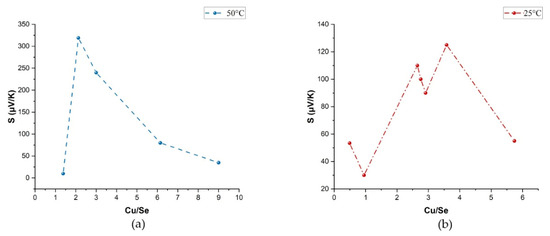
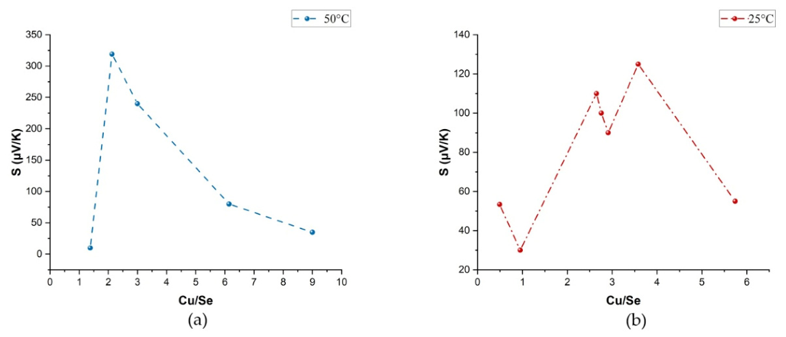
When the Cu/Se atomic ratio in the thin film gradually increases from a copper-deficient condition (<1) to a copper-rich state (>2), the phases undergo transitions through CuSe2, CuSe, β-Cu2Se, α-Cu2Se, and finally to the metallic Cu phase. It is worth noting that the β-Cu2−xSe phase, which is slightly Cu-rich near the stoichiometric ratio, usually shows the best overall thermoelectric performance, with a Cu/Se ratio of about 2.0–2.7 [26]. This is attributed to its intrinsic “phonon-glass electron-crystal” characteristics, which lead to a synergistic optimization of a high Seebeck coefficient and moderate electrical resistivity.
Changes in the elemental ratio deeply affect the carrier transport properties and microstructure of the thin films. When the Cu/Se ratio is below 2.0, the concentration of Cu vacancies increases, leading to a higher hole carrier concentration. Although electrical conductivity improves, the Seebeck coefficient decreases significantly, and the power factor drops due to the imbalance between the two. When the Cu/Se ratio exceeds 3.0, excess Cu atoms precipitate at grain boundaries or on the surface, forming metallic phases. This reduces the electrical resistivity, but the Seebeck coefficient becomes worse due to enhanced carrier scattering and the bipolar effect, so the thermoelectric performance also declines [25]. Figure 5 shows the relationship between different Cu/Se ratios and the Seebeck coefficient.
Figure 5.
The relationship between different Cu/Se ratios and the Seebeck coefficient: (a) prepared by thermal evaporation and (b) prepared by magnetron sputtering [25,26].
In addition, at the optimal Cu/Se ratio, the thin film shows dense and uniform columnar grain growth or a preferred orientation along specific axes, with the lowest surface roughness. Deviation from this ratio easily leads to multiphase coexistence, abnormal grain growth, or increased porosity, which severely degrades the electrical transport performance.
3.4. Effect of Substrate Type on Thin Film Properties
In the preparation of Cu2Se thin films, the choice of substrate material has a significant impact on their crystal structure, microstructure, and thermoelectric properties, as shown in Table 5. Different substrates, due to differences in surface energy, lattice matching, electrical conductivity, and thermal expansion coefficient, can induce different preferred orientations, crystal quality, and defect concentrations in the films, thereby tuning their final performance.
Table 5.
Effect of substrate type on thin film properties.
For flexible organic substrates, materials such as polyimide (PI) are widely used in wearable thermoelectric devices. Cu2Se thin films grown in situ on PI substrates by magnetron sputtering can induce phase transitions and optimize orientation by adjusting the Cu/Se atomic ratio. At a growth temperature of about 200 °C, these films achieve high electrical conductivity and Seebeck coefficient, and they show good mechanical flexibility [16].
Single crystal substrates enable epitaxial growth of Cu2Se thin films, leading to better thermoelectric performance. On an LSAT(100) substrate [14], films prepared by pulsed laser deposition show a b-axis preferred orientation. The room-temperature power factor reaches 8.44 μW·cm−1·K−2 and further increases to about 20 μW·cm−1·K−2 at high temperatures. The ZT value is clearly higher than that of polycrystalline bulk materials. On a Si(111) substrate [27], Cu2Se thin films tend to form a nanosheet-like structure. The grain size increases with deposition time, and the films always remain in the pure α phase, showing good control over crystal orientation.
Cu(111) single-crystal substrates have been used for epitaxial growth of Cu2Se. Molecular beam epitaxy with direct selenization at room temperature produces layered Cu2Se nanosheets with a thickness of about 38 nm. These nanosheets exhibit a hexagonal lattice, rotated 30° relative to the Cu(111) substrate. Their bandgap is 2.12 eV, indicating semiconducting behavior for optoelectronic applications [28]. This approach demonstrates that metal substrates can yield high-quality epitaxial Cu2Se films.
Metal substrates also show unique regulatory effects. A copper foil substrate [29] not only serves as the growth base but also participates in the reaction to form a dense flaky granular structure. Under low-pressure conditions, thin films with a controllable stoichiometric ratio can be prepared, and a thermoelectric voltage can be directly generated, making it suitable for simple thermoelectric conversion devices. Rare earth metal substrates, such as lanthanum [30], significantly improve the crystallinity of the films, increasing grain size and reducing defect density. They also induce a red-shift in the optical bandgap and enhance carrier mobility. The films exhibit bandpass filtering characteristics in the microwave frequency range, showing potential for application in high-frequency electronic devices.
For different application goals such as flexible wearable devices, high-performance thermoelectric conversion, or high-frequency electronic devices, choosing the right substrate material is one of the key strategies to optimize the performance of Cu2Se thin films.
Beyond conventional flat substrates, porous templates have recently become a new platform for tailoring the microstructure and thermoelectric properties of Cu2Se thin films. A recent study used anodic aluminum oxide (AAO) templates combined with thermal evaporation to prepare β-Cu2−xSe films with ordered porous structures [32]. Four pore configurations were compared: non-porous, through-hole, semi-through-hole, and sealing-pore. The sealing-pore structure was found to combine internal porosity with a dense surface layer. This structure achieves an optimal balance between suppressing heat transport and maintaining continuous carrier pathways. This work demonstrates that porous substrate engineering offers a promising strategy for further enhancing the thermoelectric performance of Cu2Se-based thin films.
In addition, reasonable changes to parameters such as the thickness of the Cu2Se thin film [33], sputtering power [34,35], deposition time [36], and pH conditions [37] can also effectively control the phase structure, grain size, stoichiometric ratio, optical band gap, and electrical transport properties of the film. This plays an important role in improving the practical performance of Cu2Se thin films.
3.5. Effect of Deposition Method on Thin Film Properties
Beyond the individual parameters discussed above, the deposition method itself significantly affects the microstructure and thermoelectric performance of Cu2Se thin films. Each technique has its own growth mechanism, energy condition, and kinetic pathway. These factors together determine crystallinity, stoichiometry, defect chemistry, and ultimately the power factor.
Physical vapor deposition methods, such as PLD and magnetron sputtering, generally produce films with superior crystallinity and density. This is attributed to the high kinetic energy of adatoms. PLD offers congruent target-to-film composition transfer at high laser fluence (~10 J/cm2). Magnetron sputtering provides precise composition control and scalability. Both methods are relatively costly and require complex equipment.
In contrast, solution-based methods such as CBD and electrodeposition are low-cost and scalable, but the resulting films typically have more defects and grain boundaries. CBD allows for easy doping during film growth. Electrodeposition enables thick films with controlled morphology. Thermal evaporation is the simplest technique. However, its composition control is limited by the high vapor pressure of Se. This often results in Cu-rich films unless the process is carefully optimized. Additionally, metal oxide thin films for optoelectronic applications have also been prepared by reactive e-beam evaporation followed by thermal annealing [38].
3.6. Synergistic Optimization of Processing Parameters
The growth temperature, annealing temperature, elemental ratio, and substrate type are not independent parameters. They are intrinsically coupled. Their synergistic effects influence the phase structure, stoichiometry, and defect chemistry of the thin films.
The high volatility of Se means that growth temperature and annealing temperature directly change the actual Cu/Se ratio of the film. When the temperature is too high, Se preferentially evaporates. This inevitably makes the film Cu-rich. It also drives the phase transformation from β-Cu2Se toward precipitation of metallic Cu. Therefore, achieving the β-Cu2Se phase with the ideal stoichiometry is not determined by the target composition alone. Instead, a dynamic balance between temperature and Cu flux must be established. When growing at higher temperatures, Cu compensation should be increased accordingly. At lower temperatures, extra compensation is not needed.
The thermal expansion mismatch between the film and the substrate causes strain during post-annealing. For example, a PI flexible substrate requires the annealing temperature to stay below 250 °C to avoid deformation. In contrast, an LSAT single-crystal substrate can tolerate up to 580 K, and this temperature even promotes b-axis orientation. Thus, the optimal annealing temperature depends strongly on the substrate, and they should be considered together.
Fabricating high-performance Cu2Se thin films cannot rely on the independent optimization of single processing parameters. Instead, all parameters must be considered as a coupled whole. Only under multi-parameter synergistic matching can the best overall performance be achieved.
4. Research Progress on Doped Cu2Se Thin Films
Doping is a key strategy to optimize the functional properties of thin film materials. It mainly introduces aliovalent ions or defects to control the electronic structure, phonon transport, and crystal stability of the material. Specifically, doping can effectively tune the carrier concentration and type and significantly improve electrical properties such as electrical conductivity and Seebeck coefficient. At the same time, doping can achieve band engineering, changing the bandgap width and band structure. In addition, point defects and heterointerfaces introduced by doping can enhance phonon scattering and reduce lattice thermal conductivity, thereby increasing the thermoelectric figure of merit ZT. Some doping can also suppress undesirable phase transitions or stabilize high-temperature phases. In the field of optoelectronic applications, doping can enhance light absorption, the separation efficiency of photogenerated carriers, and photosensitivity. For flexible electronic devices, specific doping, such as with iodine or sulfur, can significantly improve the mechanical flexibility and bending stability of the thin films [39]. The synergistic effects of these doping strategies provide an important material basis for the design of high-performance thermoelectric, optoelectronic, and wearable devices.
4.1. Effect of Carrier Concentration on Thin Film Properties
Carrier concentration refers to the number of charge carriers per unit volume that participate in electrical conduction. It is a key parameter that determines the electrical conductivity and Seebeck coefficient of a semiconductor. Table 6 and Table 7 show the effects of carrier concentration on the Seebeck coefficient and electrical conductivity, respectively.
Table 6.
Effect of carrier concentration on Seebeck coefficient.
Table 7.
Effect of carrier concentration on electrical conductivity.
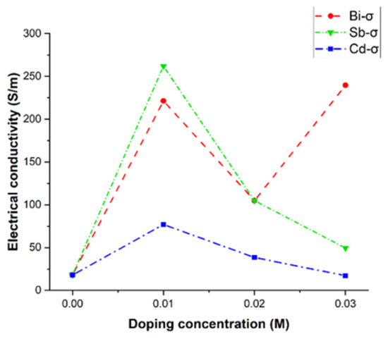
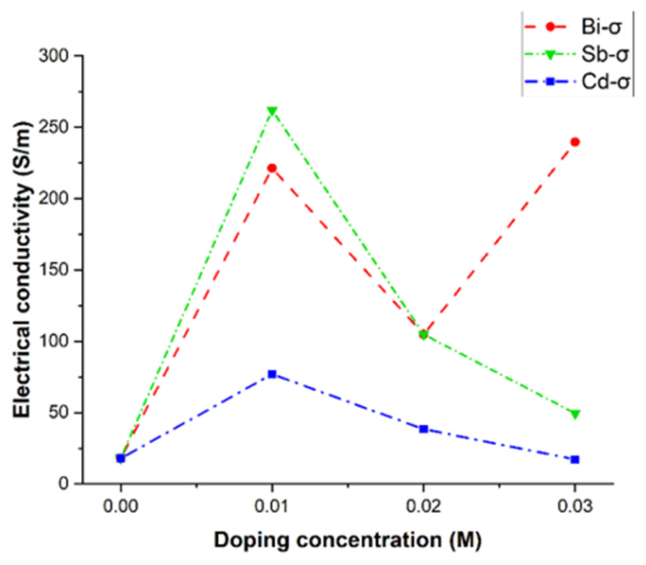
Intrinsic Cu2Se has a carrier concentration that is too high due to copper vacancy defects. Although its electrical conductivity is acceptable, its Seebeck coefficient is very low, which severely limits the power factor. Reducing the carrier concentration through donor doping such as Al [41,42], Zn [43], or I [44], or through Cu-excess strategies [50], can significantly increase the Seebeck coefficient. At the same time, point defect scattering introduced by doping reduces the thermal conductivity, achieving synergistic optimization of electrical and thermal transport properties. The CuAgSe nano-phase interfaces introduced by Ag doping and the disordered interstitial Cu+ caused by Cu-rich conditions can induce energy filtering effects and modulate carrier scattering. Within an appropriate doping range, these effects lead to an enhancement of the Seebeck coefficient [40]. Controlling the carrier concentration requires balancing the inverse relationship between electrical conductivity and the Seebeck coefficient. Moderately reducing the carrier concentration to an optimal range can achieve a high power factor. However, excessive reduction leads to a decline in electrical conductivity, which instead harms the thermoelectric performance. Figure 6 shows the relationship between the doping concentration of different elements and the electrical conductivity.
Figure 6.
The relationship between the doping concentration of different elements and the electrical conductivity [46,47,48].
Different doping elements have different regulation mechanisms. For example, Al3+ is an efficient donor dopant. It can significantly compensate for intrinsic holes and optimize the band structure. This is currently the most mature regulation strategy. Similarly, the substitution of Bi3+ at Cu+ sites introduces extra electrons. These electrons compensate intrinsic holes and reduce the hole carrier concentration. The Seebeck coefficient is enhanced. Meanwhile, Bi doping effectively suppresses the formation of Cu vacancies, further optimizing the carrier concentration. This leads to an increase in electrical conductivity [46]. The n-type compensation mechanism, such as I doping, has a relatively mild effect. However, some elements like Sb [47] and Cd [48] may produce complex defect states by substituting Cu sites, so these elements need to be carefully selected.
4.2. Effect of Band Structure on Thin Film Properties
Precise control of the band structure, including bandgap size, bandgap type, Fermi level position, and density of states distribution, can synergistically optimize carrier concentration and mobility, thereby achieving better thermoelectric performance, as shown in Table 8.
Table 8.
Band regulation methods.
Trivalent cation doping can change the bandgap type from direct to indirect, shift the Fermi level position, reduce carrier concentration, and significantly increase the Seebeck coefficient. Divalent cation doping can reduce the carrier effective mass and increase mobility, improving the Seebeck coefficient while maintaining a high electrical conductivity. This band engineering strategy successfully decouples the traditional trade-off between electrical conductivity and the Seebeck coefficient, leading to a significant increase in the power factor.
4.3. Effect of Defect Engineering on Thin Film Properties
The mechanism of defect engineering mainly lies in the synergistic regulation of carrier transport, phonon scattering, and phase stability. Intrinsic Cu vacancies, as acceptor defects, provide hole carriers, but excessive vacancies reduce mobility. Introducing aliovalent or isovalent cation doping can further optimize the band structure by forming substitutional or interstitial defects [43]. When trace magnetic elements are doped [53], the built-in magnetic field generated by interstitial defects in micro-regions can restrict the migration of low-energy carriers through the magnetic-electrical transport coupling effect. This significantly increases the carrier effective mass, thereby greatly enhancing the Seebeck coefficient and power factor.
Defect engineering is not limited to single point defect control. It also includes tuning of vacancy concentration, design of second-phase interfaces, and microstrain engineering [54]. These factors together affect the scattering processes of carriers and phonons. This is an effective way to achieve synergistic optimization of the thermoelectric properties of Cu2Se thin films.
From the perspective of optical properties, defect engineering also shows the ability to control the bandgap and absorption characteristics. Aliovalent doping can cause a shift in the optical absorption edge through quantum confinement effects and changes in carrier concentration, thereby widening or narrowing the bandgap [52]. These results indicate that the type and concentration of defects, as well as their distribution in the lattice, together determine the final properties of the thin film.
4.4. Effect of Different Dopants on Thin Film Properties
High-valent cations compensate for copper vacancies, reducing hole concentration, increasing the Seebeck coefficient, and lowering thermal conductivity. Transition metals and heavy elements optimize carrier transport. Anion substitution at Se sites tunes the band structure and lattice parameters, synergistically improving electrical conductivity and the Seebeck coefficient. Among the doping strategies discussed above, iodine and antimony doping are particularly noteworthy for their potential to enable n-type conduction in Cu2Se films. Iodine doping introduces electrons by substituting Se sites with I atoms. Each I substitution provides one extra electron. This electron compensation reduces the hole concentration. It enables a transition from p-type to n-type behavior [44]. Antimony doping offers an alternative route through band structure engineering. Theoretical calculations show that Sb substitution lowers the conduction band edge. This forms an n-type degenerate state. When combined with Ag doping, Sb further reduces the hole concentration. It also enhances the Seebeck coefficient through synergistic band modulation [55]. These studies indicate that n-type Cu2Se films can be achieved through appropriate donor doping.
Rare earth elements mainly enhance light absorption and narrow the bandgap, making them suitable for photovoltaics. Composite doping introduces multiphase interfaces, achieving a high thermoelectric figure of merit near room temperature through energy filtering and phonon scattering. The effects of different dopants on thin film properties are shown in Table 9.
Table 9.
Effects of different dopants on thin film properties.
In addition to doping with a single element, composite doping with materials such as FeSi2 can achieve synergistic optimization of polycrystalline structure, interface effects [57], and amorphous phases through control of process parameters. This leads to relatively high thermoelectric figures of merit and power factors at room temperature.
4.5. Qualitative Comparison of Different Dopants
This section provides a qualitative comparison of the most commonly reported dopants. Al3+ and Bi3+ are consistently among the most effective dopants for enhancing the thermoelectric performance of Cu2Se thin films. Their high valence state (+3) effectively compensates the intrinsic Cu vacancies and reduces the excessively high hole concentration. As a result, the Seebeck coefficient increases significantly. The electrical conductivity remains at an acceptable level.
Transition metal dopants such as Zn2+ and Co2+ offer moderate improvements. They provide additional benefits through band structure tuning and magnetic scattering. However, their effectiveness depends more strongly on the doping concentration. Anion substitution at Se sites (I−, S2−) also improves the power factor, but the enhancement is generally smaller than that of Al3+ doping. The consistent superiority of Al3+ across multiple reports suggests that hole concentration compensation is the most effective strategy for optimizing the thermoelectric performance of Cu2Se thin films.
It is worth noting that the three mechanisms—carrier concentration optimization, band engineering, and defect engineering—are not mutually exclusive. A single dopant can simultaneously influence multiple mechanisms. For example, Al3+ doping not only reduces the hole concentration through donor compensation but also modifies the electronic band structure. However, based on the literature, carrier concentration optimization appears to be the primary and most effective strategy for enhancing the thermoelectric performance of Cu2Se thin films. This is because Cu2Se intrinsically has an excessively high hole concentration (~1021 cm−3) due to Cu vacancies. Reducing this concentration to an optimal level yields the most significant improvement in the Seebeck coefficient and power factor.
Band engineering and defect engineering serve as complementary strategies. They provide additional enhancements through band structure tuning, phonon scattering, and mobility optimization. However, their effects are generally less pronounced than carrier concentration optimization. The consistently superior performance of Al3+ doping across multiple reports supports this view. Al3+ is effective primarily because it efficiently compensates the intrinsic Cu vacancies.
Therefore, all three mechanisms contribute to performance improvement. However, carrier concentration optimization should be considered the primary strategy. Band engineering and defect engineering are supplementary approaches. The optimal overall performance is achieved when these strategies are applied synergistically.
5. Conclusions
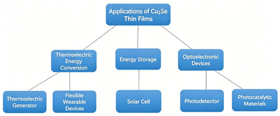
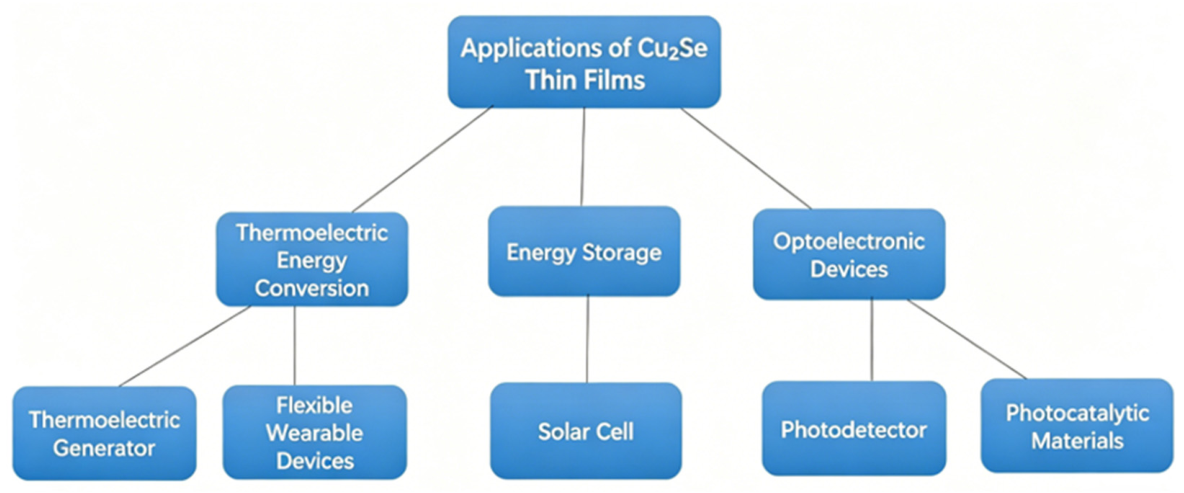
Cu2Se is a p-type semiconductor compound composed of copper and selenium. It has low cost, environmental friendliness, and excellent optoelectronic and thermoelectric properties. It is an important candidate system to replace traditional lead-based and tellurium-based functional materials. Table 10 compares the power factor, toxicity, and cost of representative thermoelectric thin films. The main applications of Cu2Se focus on thermo-electric conversion, optoelectronic devices [58], and energy storage, as shown in Figure 7. As a medium- to high-temperature thermoelectric material, its ZT value can exceed 2.0. After being fabricated into thin films, it can be used in micro thermoelectric generators and flexible wearable devices for waste heat recovery and solid-state cooling [59,60,61]. In the fields of optoelectronics and energy storage, its high absorption in the visible region and tunable bandgap make it a potential component for solar cells, photodetectors, and photocatalytic materials. In addition, Cu2Se can be used as an anode material for sodium-ion batteries and as an electrocatalytic material for quantum dot-sensitized solar cells [62].
Table 10.
Comparison of power factor, toxicity, and cost for representative thermoelectric thin films [7].
Figure 7.
Applications of Cu2Se thin films.
Of note, bulk thermoelectric materials currently dominate large-scale applications due to their well-established synthesis routes and high reproducibility. Cu2Se thin films are not meant to replace bulk materials. They are particularly suitable for emerging applications such as flexible/wearable devices, on-chip micro-generators, and semiconductor integration, where bulk materials are impractical.
In recent years, the p-Cu2Se/n-Si heterojunction based on Cu2Se thin films has shown good rectification characteristics and a band structure similar to a Schottky diode. It exhibits excellent self-powered photoresponse with fast speed, high stability, and good reproducibility, making it suitable for high-frequency photodetectors. This heterojunction also achieves high power conversion efficiency in photovoltaic devices, outperforming previously reported CuO/Si and Cu2O/Si systems, indicating its broad application potential in optoelectronics [11]. In photovoltaics, Cu2Se thin films serve as hole transport layers or absorber layers. The achievable power conversion efficiency ranges from 1% to 5%. The exact value depends on the stoichiometry and crystallinity of the films. For photocatalysis, Cu2Se films show moderate degradation of organic dyes under visible light, but their quantum efficiency remains lower than that of well-established materials such as TiO2. Overall, Cu2Se shows clear potential in photodetection and photovoltaics. However, its photocatalytic efficiency requires further improvement. Currently, cross-comparisons among different applications are insufficient. Future work should focus on objectively evaluating the performance of Cu2Se thin films across various optoelectronic applications.
This paper has reviewed the recent progress in the thermoelectric properties of Cu2Se thin films prepared by different methods. The first part introduces the structure and properties of Cu2Se. The second part analyzes how key process parameters control the phase structure, grain size, and properties of the films. The third part reviews the optimization effects of different element doping on film properties, revealing that doping is the most effective way to improve the performance of Cu2Se thin films. Finally, the paper summarizes the application progress of Cu2Se thin films, providing a reference for future researchers to prepare high-performance Cu2Se materials.
Although many advances have been made in the production of Cu2Se thin films, some challenges and issues remain:
- Preparation process and reproducibility
Different preparation methods are highly sensitive to process parameters, leading to large differences in film morphology, orientation, and properties, as well as poor batch-to-batch reproducibility. At present, large-area uniform deposition and high-quality growth on flexible substrates remain difficult.
- 2.
- Oxidation and thermal stability
High-temperature treatment in air or long-term exposure can easily cause oxidation of the Cu2Se surface, forming CuO or Cu2O. This introduces insulating phases and degrades the electrical conductivity and Seebeck coefficient. How to improve environmental stability while maintaining performance is a key bottleneck for practical applications.
- 3.
- Interface stability between Cu2Se films and metal electrodes
The interface stability between Cu2Se films and metal electrodes remains poorly understood. Cu ions tend to migrate toward the electrode interface during operation. This increases contact resistance and degrades device performance. Systematic studies on interface degradation and long-term reliability are still lacking.
To address these issues, several strategies have been reported. For thermal cycling stability, Al doping and W nanoinclusion have been shown to stabilize the thermoelectric performance [63]. For long-term stability, Cu2Se thin films have been demonstrated to retain good performance after ambient storage [64]. Oxidation resistance is another concern. A surface organic coating can effectively prevent degradation during bending [65]. Cu-ion migration is a key instability factor. It can be suppressed by the formation of an oxide surface layer during operation in air. It can also be inhibited by Te substitution, which increases the migration energy barrier [66]. These studies suggest that reliability challenges exist, but effective solutions are being developed.
Challenges persist, yet recent progress summarized in this review indicates that these issues are being progressively addressed through composition optimization, rational doping, and substrate engineering. In summary, as a highly promising material, the performance breakthrough of Cu2Se thin films relies on coordinated innovation in material processing and synergistic optimization of various preparation parameters, ultimately promoting their large-scale applications in thermoelectric and optoelectronic devices.
Author Contributions
Conceptualization, Y.F. and Z.G.; methodology, X.L.; writing—original draft preparation, Y.F. and Y.X.; writing—review and editing, X.C. and C.H.; visualization, Y.Y., F.T. and K.L.; supervision, Z.L., Y.Q. and L.L.; funding acquisition, Y.Q. All authors have read and agreed to the published version of the manuscript.
Funding
This work was supported in part by specific research fund for Innovation Platform for Academicians of Hainan Province (No. YSPTZX202513); in part by the National Natural Science Foundation of China (No. 62464006); in part by the Key Research and Development Projects in Hainan Province (No. ZDYF2025GXJS007); in part by Hainan Province International Science and Technology Cooperation R&D Project (No. GHYF2025030); in part by the Foreign Experts Project of Hainan Province (No. H20260407006E); in part by Scientific Research Projects of Hainan Province’s Flexible Talent Introduction Innovation Platform (No. RXPTXM202609).
Institutional Review Board Statement
Not applicable.
Informed Consent Statement
Not applicable.
Data Availability Statement
No new data were created or analyzed in this study. Data sharing is not applicable to this article.
Conflicts of Interest
The authors declare no conflict of interest.
References
- Yang, D.; Su, X.; Li, J.; Bai, H.; Wang, S.; Li, Z.; Tang, H.; Tang, K.; Luo, T.; Yan, Y. Blocking ion migration stabilizes the high thermoelectric performance in Cu2Se composites. Adv. Mater. 2020, 32, 2003730. [Google Scholar] [CrossRef] [Scilit]
- Yadav, B.K.; Singh, P.; Yadav, C.P.; Pandey, D.K.; Singh, D. Structural and wavelength dependent optical study of thermally evaporated Cu2Se thin films. Z. Naturforschung A 2020, 75, 781–788. [Google Scholar] [CrossRef] [Scilit]
- Li, H.; Li, F.; Chen, Y.; Liang, G.; Luo, J.; Wei, M.; Zheng, Z.; Zheng, Z. Optimization of thermoelectric properties and physical mechanisms of Cu2Se-based thin films via heat treatment. Nanomaterials 2024, 14, 1421. [Google Scholar] [CrossRef] [Scilit] [PubMed]
- Huang, X.; Ao, D.; Chen, T.; Chen, Y.; Li, F.; Chen, S.; Liang, G.; Zhang, X.; Zheng, Z.; Fan, P. High-performance copper selenide thermoelectric thin films for flexible thermoelectric application. Mater. Today Energy 2021, 21, 100743. [Google Scholar] [CrossRef] [Scilit]
- Rapaka, S.S. Thermoelectric Studies of Modified Cu2Se: Bulk and Thin Film for Waste Heat Recovery. Ph.D. Thesis, RMIT University, Melbourne, Australia, 2025. [Google Scholar]
- Lin, Z.; Hollar, C.; Kang, J.S.; Yin, A.; Wang, Y.; Shiu, H.Y.; Huang, Y.; Hu, Y.; Zhang, Y.; Duan, X. A solution processable high-performance thermoelectric copper selenide thin film. Adv. Mater. 2017, 29, 1606662. [Google Scholar] [CrossRef] [Scilit]
- Nandihalli, N. Thermoelectric films and periodic structures and spin Seebeck effect systems: Facets of performance optimization. Mater. Today Energy 2022, 25, 100965. [Google Scholar] [CrossRef] [Scilit]
- Ali, S.; Hassun, H.; Salih, A.; Athabb, R.; Al-Maiyaly, B.; Hussein, B. Study the properties of Cu2Se thin films for optoelectronic applications. Chalcogenide Lett. 2022, 19, 663–671. [Google Scholar] [CrossRef] [Scilit]
- Chi, H.; Kim, H.; Thomas, J.C.; Shi, G.; Sun, K.; Abeykoon, M.; Bozin, E.S.; Shi, X.; Li, Q.; Shi, X. Low-temperature structural and transport anomalies in Cu2Se. Phys. Rev. B 2014, 89, 195209. [Google Scholar] [CrossRef] [Scilit]
- Lu, P.; Liu, H.; Yuan, X.; Xu, F.; Shi, X.; Zhao, K.; Qiu, W.; Zhang, W.; Chen, L. Multiformity and fluctuation of Cu ordering in Cu2Se thermoelectric materials. J. Mater. Chem. A 2015, 3, 6901–6908. [Google Scholar] [CrossRef] [Scilit]
- Lin, D.; Shih, Y.; Qiu, D.; Kao, Y.; Hwang, S.; Kao, M.; Lin, C. Facile synthesis and characterization of Cu2Se thin films and self-powered p-Cu2Se/n-Si heterojunction with high-performance photoresponse. J. Phys. D Appl. Phys. 2024, 57, 435104. [Google Scholar] [CrossRef] [Scilit]
- Byeon, D.; Sobota, R.; Delime-Codrin, K.; Choi, S.; Hirata, K.; Adachi, M.; Kiyama, M.; Matsuura, T.; Yamamoto, Y.; Matsunami, M. Discovery of colossal Seebeck effect in metallic Cu2Se. Nat. Commun. 2019, 10, 72. [Google Scholar] [CrossRef] [Scilit] [PubMed]
- Zhu, B.; Liu, X.; Wang, Q.; Qiu, Y.; Shu, Z.; Guo, Z.; Tong, Y.; Cui, J.; Gu, M.; He, J. Realizing record high performance in n-type Bi2Te3-based thermoelectric materials. Energy Environ. Sci. 2020, 13, 2106–2114. [Google Scholar] [CrossRef] [Scilit]
- Wang, A.; Xue, Y.; Wang, J.; Yang, X.; Wang, J.; Li, Z.; Wang, S. High thermoelectric performance of Cu2Se-based thin films with adjustable element ratios by pulsed laser deposition. Mater. Today Energy 2022, 24, 100929. [Google Scholar] [CrossRef] [Scilit]
- Li, Y.; Zhong, Y.; Zhang, D.; Niu, J.; Nisar, M.; Wei, M.; Liang, G.; Fan, P.; Zheng, Z. Enhanced thermoelectric properties of Cu2Se flexible thin films by optimizing growth temperature and elemental composition. ACS Appl. Energy Mater. 2022, 5, 13964–13970. [Google Scholar] [CrossRef] [Scilit]
- Li, Z.; Wang, J.; Yang, X.; Gao, Z.; Xue, Y.; Wang, J.; Wang, S. Flexible oriented α-Cu2Se films and devices with remarkable power factor and output power at near-room temperature. Mater. Today Phys. 2023, 31, 100994. [Google Scholar] [CrossRef] [Scilit]
- Rapaka, S.S.; Anwar, S.; Anwar, S. Evaluation of substrate temperature role on the structural, morphological, optical, and mechanical properties of magnetron sputtered Cu2Se thin films. Mater. Sci. Eng. B 2024, 301, 117142. [Google Scholar] [CrossRef] [Scilit]
- Rapaka, S.S.; Anwar, S.; Anwar, S. Optimizing thermoelectric power factor in magnetron sputtered Cu2Se thin films by varying substrate temperature and synergy of Cu/Se ratio. Ceram. Int. 2024, 50, 15879–15887. [Google Scholar] [CrossRef] [Scilit]
- Hadi, S.M.; Al-Maiyaly, B.K. Optical and Morphology Properties of Cu2Se at Different Temperatures by Thermal Evaporation. Ibn AL-Haitham J. Pure Appl. Sci. 2025, 38, 159–168. [Google Scholar] [CrossRef] [Scilit]
- Henry, J.; Daniel, T.; Balasubramanian, V.; Mohanraj, K.; Sivakumar, G. Temperature dependent electrical and optical properties with higher photosensitivity of Cu2Se absorber thin films for photo voltaic application. Inorg. Nano-Metal. Chem. 2021, 51, 38–46. [Google Scholar]
- Francis, M.; Kuruvilla, A. Effect of annealing on chemically deposited Cu2Se thin films. Mater. Chem. Phys. 2022, 292, 126845. [Google Scholar] [CrossRef] [Scilit]
- Roldan, T.; Méndez-Blas, A.; López-Cruz, E.; Calixto, M. Semiconducting Cu2Se thin films obtained by electrochemical deposition for possible applications in thermoelectric systems. MRS Adv. 2022, 7, 1–4. [Google Scholar] [CrossRef] [Scilit]
- Rapaka, S.S.; Anwar, S.; Anwar, S. Augmentation of Thermoelectric Power Factor in the Magnetron Sputtered Cu2Se Thin Films by Controlled Annealing. Ceram. Int. 2025, 51, 52935–52944. [Google Scholar] [CrossRef] [Scilit]
- Liu, J.; Wu, G.; Wang, Y.; Xiao, J.; Jiang, A. Structure and properties of cuprous selenide films prepared by sputtering and selenization. Appl. Surf. Sci. 2025, 719, 165053. [Google Scholar] [CrossRef] [Scilit]
- Wu, Z.; Wu, J.; Li, Y.; Li, G. Effect of Cu content on electrical properties of evaporated Cu-Se thermoelectric films. Ceram. Int. 2020, 46, 21617–21622. [Google Scholar] [CrossRef] [Scilit]
- Li, G.; Song, G.; Wang, N.; Hu, F.; Wu, Y.; Du, H.; Yuo, J. Influence of Cu content on the phase composition and thermoelectric properties of deposited Cu-Se films. Surf. Interfaces 2022, 28, 101651. [Google Scholar] [CrossRef] [Scilit]
- Zhou, L.; Li, Q.; Jin, M.; Zhang, R.; Zhang, Q. Preparation of (111) c-oriented Cu2Se films by pulsed laser deposition method. Thin Solid Films 2022, 741, 139024. [Google Scholar] [CrossRef] [Scilit]
- Song, Z.; Yi, J.; Shi, J.; Xu, H.; Bian, C.; Shen, C.; Zhang, Y.; Zhou, W.; Du, S.; Lu, H. Epitaxial Semiconducting Cu2Se Nanosheets on Cu (111) Substrates Using Direct Deep Selenization. ACS Appl. Nano Mater. 2024, 7, 17729–17735. [Google Scholar] [CrossRef] [Scilit]
- Hua, X.; Li, J.; Liu, H.; Zhang, C.; Han, Y.; Gao, F.; Hodes, G.; Wang, P.; Yang, Z.; Liu, S.F. Preparation of Cu2Se thin films by vacuum evaporation and hot-pressing. Vacuum 2021, 185, 109947. [Google Scholar] [CrossRef] [Scilit]
- Qasrawi, A.F.; Ghannam, A.N.A. Effect of lanthanum substrates on the structural, optical and electrical properties of copper selenide thin films designed for 5G technologies. Opt. Quantum Electron. 2022, 54, 4. [Google Scholar] [CrossRef] [Scilit]
- Thanikaikarasan, S. Structural and optical properties of electrodeposited Cu2Se thin films. Mater. Today Proc. 2020, 33, 3399–3401. [Google Scholar] [CrossRef] [Scilit]
- Sun, S.; Lan, M.; Li, G.; Liu, S.; Zhu, J.; Wang, K.; Wang, Q. Evolution of thermoelectric properties in Cu2−xSe films with ordered porous structures. Scr. Mater. 2026, 275, 117183. [Google Scholar] [CrossRef] [Scilit]
- Jadav, D.J.; Varasada, R.; Trasadiya, M.; Vyas, S.; Vora, A. Synthesize and Investigate Structural, Surface Morphology, Optical, and Electrical Characterization of Cu2Se Thin Films by Thermal Evaporation Technique. Braz. J. Phys. 2024, 54, 246. [Google Scholar] [CrossRef] [Scilit]
- Rapaka, S.S.; Anwar, S.; Priyadarshini, B.; Anwar, S. The effect of sputtering power on structural, mechanical, and electrical properties of Copper Selenide Thermoelectric thin films deposited by magnetron sputtering. Mater. Chem. Phys. 2023, 304, 127879. [Google Scholar] [CrossRef] [Scilit]
- Wu, G.; Liu, J.; Zhou, C.; Zhang, X.; Xu, Z.; Xiao, J. Investigation on the regulation of copper vacancy defects and dielectric properties of β-Cu2Se thin films by sputtering power. Colloids Surf. A Physicochem. Eng. Asp. 2026, 746, 140766. [Google Scholar] [CrossRef] [Scilit]
- Takaza, C.; Fukunaka, Y.; Homma, T. Influence of Deposition Duration on the Morphological Evolution of Electrodeposited Copper Selenide Films. Electrochemistry 2026, 94, 017003. [Google Scholar] [CrossRef] [Scilit]
- Takaza, C.; Fukunaka, Y.; Homma, T. Electrodeposition Process for Optimizing Cu2Se Films with Controlled Surface Morphology and Structural Properties. ACS Omega 2025, 10, 48798–48807. [Google Scholar] [CrossRef] [Scilit] [PubMed]
- Hossain, M.I.; Chelvanathan, P.; Aissa, B.; Khandakar, A.; Rahman, A.; Mansour, S. Enhanced perovskite solar cells performance with TiOx and SnOx thin films as electron transport layers. Sci. Rep. 2025, 15, 7709. [Google Scholar] [CrossRef] [Scilit] [PubMed]
- Nguyen, K.T.; Dong, L.A.; Dinh, H.T.; Bui, T.H.T.; Chu, S.T.; Nguyen-Tran, T.; Hoang, C.H.; Nguyen, H.Q. Optimization and Characterization of Thermoelectric Properties in Selenium-Doped Bismuth Telluride Ultra Thin Films. arXiv 2024, arXiv:2410.20705. [Google Scholar]
- Song, G.; Li, G.; Li, X.; Du, H.; Hu, F. Thermoelectric performance of copper-rich β-Cu2Se films with Ag-doping by magnetron sputtering. Mater. Chem. Phys. 2021, 260, 124143. [Google Scholar] [CrossRef] [Scilit]
- Yang, D.; Zhang, D.; Ao, D.; Nisar, M.; Mansoor, A.; Chen, Y.; Li, F.; Ma, H.; Liang, G.; Zhang, X. High thermoelectric performance of aluminum-doped cuprous selenide thin films with exceptional flexibility for wearable applications. Nano Energy 2023, 117, 108930. [Google Scholar] [CrossRef] [Scilit]
- Chen, T.; Yang, D.; Li, H.; Liu, Q.; Cai, Z.; Chen, C.; Ao, D.; Ma, H.; Zhang, X. Optimization of thermoelectric power factor in β-Cu2Se thin films through Al doping. Surf. Interfaces 2025, 71, 106958. [Google Scholar] [CrossRef] [Scilit]
- Chen, T.; Sun, L.; Li, H.; Liu, Q.; Cai, Z.; Chen, C.; Ao, D.; Liang, G.; Zheng, Z. Zn-Doping-Enabled Carrier Optimization and Band Engineering for High-Performance Thermoelectric Cu2Se Thin Films. J. Alloys Compd. 2025, 1044, 184290. [Google Scholar] [CrossRef] [Scilit]
- Wang, J.; Zhang, M.; Li, J.; Wu, C.; Cai, K. Enhanced thermoelectric performance of flexible Cu2Se films via doping iodine. ACS Appl. Mater. Interfaces 2025, 17, 39312–39318. [Google Scholar] [CrossRef] [Scilit] [PubMed]
- Sudha, A.; Henry, J.; Mohanraj, K.; Sivakumar, G. Effect of Na doping on structural, optical, and electrical properties of Cu2Se thin films prepared by chemical bath deposition method. Appl. Phys. A 2018, 124, 164. [Google Scholar] [CrossRef] [Scilit]
- Henry, J.; Daniel, T.; Balasubramanian, V.; Mohanraj, K.; Sivakumar, G. Enhanced photosensitivity of Bi-doped Cu2Se thin films prepared by chemical synthesis for solar cell application. Iran. J. Sci. Technol. Trans. A Sci. 2020, 44, 1369–1377. [Google Scholar] [CrossRef] [Scilit]
- Henry, J.; Daniel, T.; Balasubramanian, V.; Mohanraj, K.; Sivakumar, G. Electrical and optical properties of Sb-doped Cu2Se thin films deposited by chemical bath deposition. Phase Transit. 2020, 93, 793–801. [Google Scholar] [CrossRef] [Scilit]
- Henry, J.; Daniel, T.; Balasubramanian, V.; Mohanraj, K.; Sivakumar, G. Synthesis and characterisation of Cu2Se thin films doped with divalent cation (Cd2+) by the chemical bath deposition method. Phase Transit. 2021, 94, 567–576. [Google Scholar] [CrossRef] [Scilit]
- Wang, J.; Li, J.; Liu, Y.; Zhang, M.; Wu, C.; Wang, Z.; Zuo, X.; Han, X.; Cai, K. Largely enhanced performance of Cu2Se film by doping sulfur for flexible thermoelectric generators. Mater. Today Phys. 2024, 43, 101422. [Google Scholar] [CrossRef] [Scilit]
- Zheng, Z.; Zhang, D.; Jabar, B.; Chen, T.; Nisar, M.; Chen, Y.; Li, F.; Chen, S.; Liang, G.; Zhang, X. Realizing high thermoelectric performance in highly (0l0)-textured flexible Cu2Se thin film for wearable energy harvesting. Mater. Today Phys. 2022, 24, 100659. [Google Scholar] [CrossRef] [Scilit]
- He, H.; Lu, J. Chemical Bath Deposition of Undoped and Bi-doped n-Cu2Se Films and their Optoelectrical Properties. Nanosci. Nanotechnol.-Asia 2018, 8, 208–215. [Google Scholar] [CrossRef] [Scilit]
- Sudha, A.; Henry, J.; Mohanraj, K.; Sivakumar, G. Synthesis and characterization of monovalent, divalent and trivalent cation doping of Cu2Se thin films using chemical bath deposition method. Jordan J. Phys. 2018, 11, 125–130. [Google Scholar]
- Liu, L.; Zhang, J.; Bai, X.; Liu, S. Co dopant enhance the thermoelectric properties of Cu2Se films via magnetism and smooth surface. Mater. Sci. Semicond. Process. 2026, 202, 110116. [Google Scholar] [CrossRef] [Scilit]
- Zhai, G.; Lan, M.; Liu, S.; Li, G.; Wang, Z.; Wang, Q. Effect of Cu distribution on thermoelectric properties of evaporated Cu2− xSe films with various Ag contents. J. Alloys Compd. 2023, 944, 169158. [Google Scholar] [CrossRef] [Scilit]
- Zhang, H.; Zhao, L.; Wang, J.; Zhang, G.; Cao, Q.; Ding, Z.; Wang, S.; Wang, J.; Li, Z. Unlocking enhanced thermoelectric performance in Cu2Se: The synergistic effects of Ag and Sb co-doping and band structure optimization. Appl. Mater. Today 2025, 44, 102783. [Google Scholar] [CrossRef] [Scilit]
- Akpu, N.I.; Asiegbu, A.D.; Nnanna, L.A.; Ikhioya, I.L.; Mgbeojedo, T.I. Synthesis and characterization of novel yttrium-incorporated copper selenide (CuSe: Y) thin materials for solar energy applications. J. Mater. Sci. Mater. Electron. 2022, 33, 1154–1161. [Google Scholar]
- Goto, M.; Sasaki, M.; Moronaga, T.; Hara, T.; Xu, Y. Room-temperature FeSi2-doped Cu2Se thermoelectric films with enhanced figure of merit. Sci. Rep. 2025, 15, 27278. [Google Scholar] [CrossRef] [Scilit] [PubMed]
- Lee, W.; Myung, N.; Rajeshwar, K.; Lee, C. Electrodeposition of Cu2Se semiconductor thin film on Se-modified polycrystalline Au electrode. J. Electrochem. Sci. Technol. 2013, 4, 140–145. [Google Scholar] [CrossRef]
- Lu, X.; Jiang, P.; Bao, X. Phonon-enhanced photothermoelectric effect in SrTiO3 ultra-broadband photodetector. Nat. Commun. 2019, 10, 138. [Google Scholar] [CrossRef] [Scilit] [PubMed]
- Snyder, G.J.; Toberer, E.S. Complex thermoelectric materials. Nat. Mater. 2008, 7, 105–114. [Google Scholar] [CrossRef] [Scilit] [PubMed]
- Pei, Y.; Shi, X.; LaLonde, A.; Wang, H.; Chen, L.; Snyder, G.J. Convergence of electronic bands for high performance bulk thermoelectrics. Nature 2011, 473, 66–69. [Google Scholar] [CrossRef] [Scilit] [PubMed]
- Mane, R.; Kajve, S.; Lokhande, C.; Han, S. Studies on p-type copper (I) selenide crystalline thin films for hetero-junction solar cells. Vacuum 2006, 80, 631–635. [Google Scholar] [CrossRef] [Scilit]
- Bohra, A.K.; Bhatt, R.; Singh, A.; Bhattacharya, S.; Basu, R.; Bhatt, P.; Navaneethan, M.; Sarkar, S.K.; Anwar, S.; Muthe, K.P. Stabilizing Thermoelectric Figure-of-Merit of Superionic Conductor Cu2Se through W Nanoinclusions. Phys. Status Solidi (RRL) –Rapid Res. Lett. 2020, 14, 2000102. [Google Scholar] [CrossRef] [Scilit]
- Khuncharoen, W.; Theekhasuk, N.; Rudradawong, C.; Voraud, A.; Sakdanuphab, R.; Sakulkalavek, A. Tuning the thermoelectric performance of flexible copper selenide thin films through sputtering pressure and hybrid microwave annealing. J. Alloys Compd. 2025, 1041, 183742. [Google Scholar] [CrossRef] [Scilit]
- Nieroda, P.; Rudnik, M.; Mitoraj-Królikowska, M.; Drożdż, E.; Kozień, D.; Leszczyński, J.; Koleżyński, A. Investigating the Stability of Cu2Se Superionic Thermoelectric Material in Air Atmosphere. Materials 2025, 18, 4152. [Google Scholar] [CrossRef] [Scilit] [PubMed]
- Saini, R.; Paul, S.; Aggarwal, S.; Maiti, T.; Pati, S.K.; Mallik, R.C. Enhanced thermoelectric performance of Cu2Se through Cu-deficiency and Te-substitution. J. Mater. Chem. C 2025, 13, 18690–18701. [Google Scholar] [CrossRef] [Scilit]

Disclaimer/Publisher’s Note: The statements, opinions and data contained in all publications are solely those of the individual author(s) and contributor(s) and not of MDPI and/or the editor(s). MDPI and/or the editor(s) disclaim responsibility for any injury to people or property resulting from any ideas, methods, instructions or products referred to in the content. |
© 2026 by the authors. Licensee MDPI, Basel, Switzerland. This article is an open access article distributed under the terms and conditions of the Creative Commons Attribution (CC BY) license.