


Abstract
In this paper, the physical properties of a new series of multilayer structures of oxide/metal/oxide type deposited on glass and plastic substrates were studied in the context of their use as transparent conductive layers for solar cells. The optical properties of TiO2/Ag/TiO2, TiO2:Nb/Ag/TiO2:Nb and NiO/Ag/NiO tri-layers were investigated by spectrophotometry and ellipsometry. Optimized ellipsometric modeling was employed in order to correlate the optical and electrical properties with the ones obtained by direct measurements. The wetting surface properties of single layers (TiO2, TiO2:Nb and NiO) and tri-layers (TiO2/Ag/TiO2 TiO2:Nb/Ag/TiO2:Nb and NiO/Ag/NiO) were also studied and good correlations were obtained with their morphological properties.
1. Introduction
In the class of transparent conducting electrodes, there are few highly-doped oxides that are typically used as single layers of about 100 to 200 nm for electronics and solar cell applications [1]. Among these, the most well-known is Sn-doped In2O3 (ITO–indium tin oxide). Due to its intensive use and extremely limited resources on Earth, indium is one of the most economically important critical raw materials [2]. Hence, alternative solutions for ITO have been intensively looked for. A lot of studies have been done on Al, In and Ga-doped ZnO (AZO, IZO and GZO) thin films, and on F-doped SnO2 (FTO) [3,4,5,6,7,8,9,10,11,12,13]. Besides, in the last few years, a new class of electrodes including ITO/Au/ITO, ITO/Ag/ITO, ZnO/Au/ZnO, AZO/Au/AZO and Bi2O3/Au/Bi2O3 [14,15,16,17] was developed on plastic substrates for OPV applications [18,19]. A lot of studies were also done on using TiO2/Ag/TiO2 as an electrode, especially for DSSC applications and perovskite solar cells, due to such electrodes’ energy conversion efficiency [20,21,22,23,24,25,26,27,28,29,30]. These oxide/metal/oxide (O/M/O) electrodes have many advantages, due to their suitability for deposition on flexible substrates. Of their favorable mechanical properties, the metallic layer’s ductility is notable. The necessary quantity of oxide materials is generally reduced by two or three times; hence, the total electrode film’s thickness can be reduced. The oxide layers act as protective coatings against the oxidation and mechanical degradation of the metallic interlayer film. For solar cell applications, the surface film’s properties positively influence the values of the extraction potential.
The novelty of this study consists in its comprehensive analysis of a new class of oxide/metal/oxide electrodes, including TiO2:Nb/Ag/TiO2:Nb and NiOx/Ag/NiOx (for simpler reading, we use the notation NiO/Ag/NiO for the last structure), which were deposited on plastic and glass substrates by sputtering from metallic targets.
Indeed, very few studies have been done on TiO2:Nb/Ag/TiO2:Nb [31,32] and NiO/Ag/NiO [33,34,35]. Recently, it was proved that the NiO/Ag/NiO antireflective multilayer electrodes used as top cathodes [33], bottom electrodes for CH3NH3PBI3 perovskite solar cells [34], or bottom electrodes for PBDTTT-C:PCBM organic solar cells, have improved efficiency compared to the industry standard [35]. To further this important progress for organic and perovskite solar cells, the purpose of this paper is to give a complete and comparative overview of the physical properties of three of these new electrodes: TiO2/Ag/TiO2, TiO2:Nb/Ag/TiO2:Nb and NiO/Ag/NiO.
2. Materials and Methods
The study involved the preparation and analysis of three sets of samples, including single layers and three-layer oxide/metal/oxide structures deposited on plastic (HIFIPMX739 PET) and glass substrates. Thin oxide films and the metallic interlayer film were deposited by DC magnetron sputtering in reactive and argon atmospheres, respectively, using different metallic targets. The deposition was performed at room temperature in a vertical target–substrate configuration. The deposition parameters were the same regardless of the structures with which the layers were involved, which are mentioned in Table 1. They were chosen taking in account the optimal values in order to obtain simultaneously good optical and electrical properties.
Table 1.
Deposition conditions for the samples.
The morphological properties were analyzed by electron microscopy and atomic force microscopy using a CP-R, Veeco thermo-microscope (CSInstruments, Les Ulis, France) and a JEOL JSM 6301F Electronic Microscope (JEOL, Croissy-sur-Seine, France). The wetting properties were studied via contact angle measurements performed at room temperature using distillated water droplets of equal volumes (3 µL). The optical properties were investigated on both single oxide layers and oxide/metal/oxide layers, using several techniques. Information regarding the transmission and reflection spectra was recorded using a double beam UV/VIS S9000 (Labomoderne, Gennevilliers, France) spectrophotometer and an AvaSpec-3648 Avantes optical fiber spectrophotometer (Avantes, Apeldoorn, The Netherlands), respectively. The optical properties were studied in a 300–1100 nm wavelength range. For instance, the amplitude (ψ) and phase difference (Δ) spectra were registered by spectroscopic ellipsometry using an UVISEL NIR Horiba Jobin Yvon ellipsometer (Horiba Jobin Yvon, Longjumeau, France) equipped with a 75 W high discharge Xe lamp. The chosen configurations for the modulator (M), analyzer (A) and polarizer (P) positions were: M = 0° and A = 45°; the incidence angle was AOI = 70°. The experimental data were fitted by modelling using the Delta Psi 2 software from Horiba Jobin Yvon (Horiba Jobin Yvon, Longjumeau, France). The optimization of the models was done by following the procedure described in [17]. The electrical conductivity measurements were done using four-point method in planar geometry at room temperature using a Keithley 2600 source Metter (RS Components Ltd., Northants, UK), by measuring the total (sheet) resistance of the multilayer structure. The distance between the probe tips was 0.635 mm. The electrical conductivity was calculated using the estimated value of thickness obtained by ellipsometry for the three-layer structure.
3. Results and Discussion
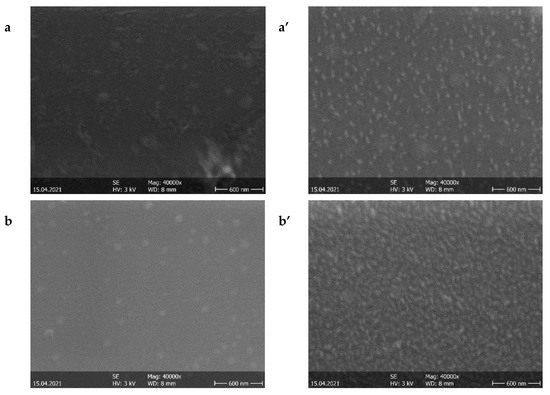
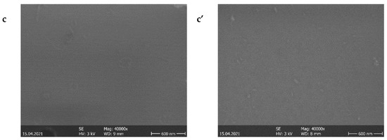
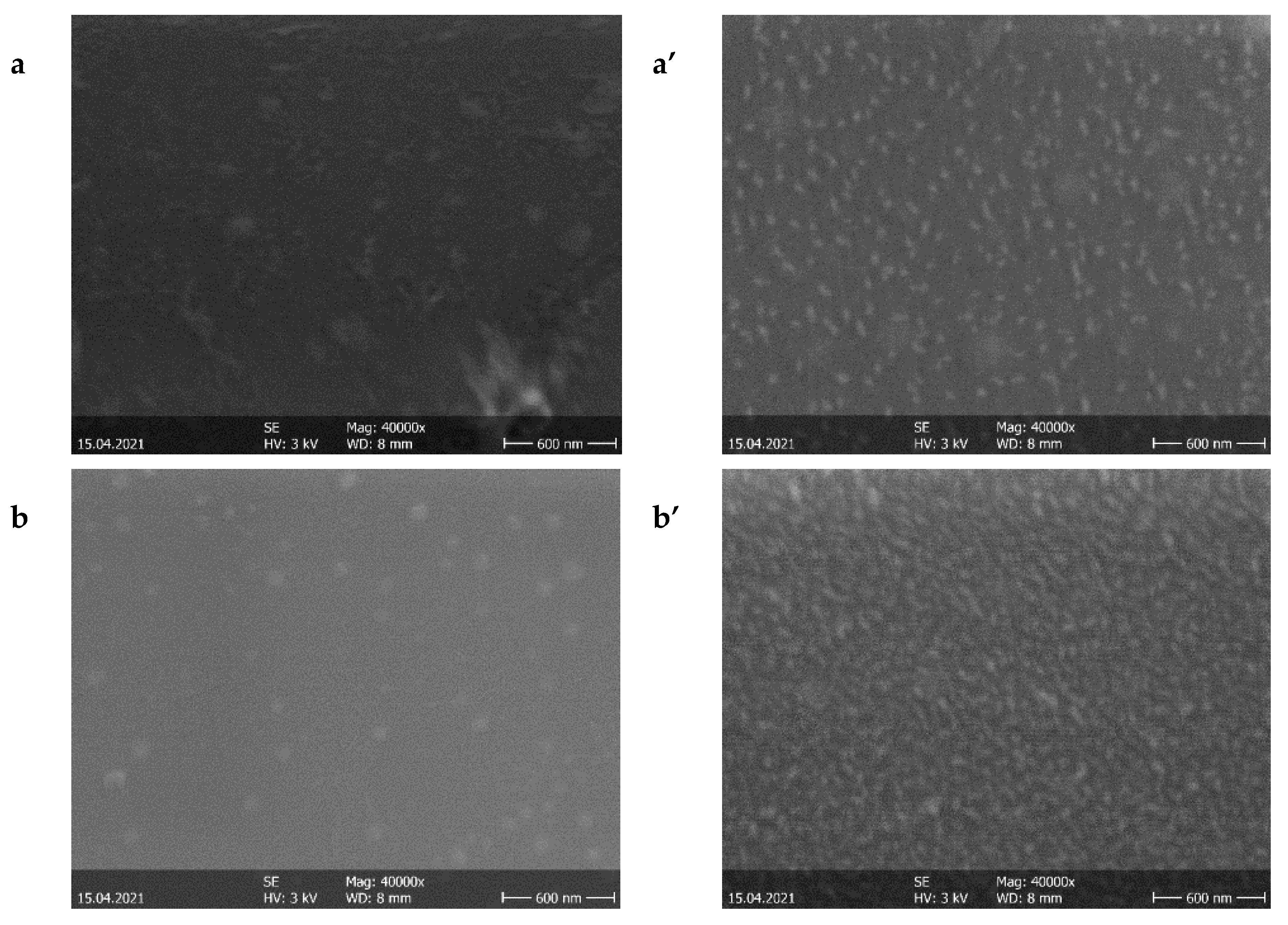
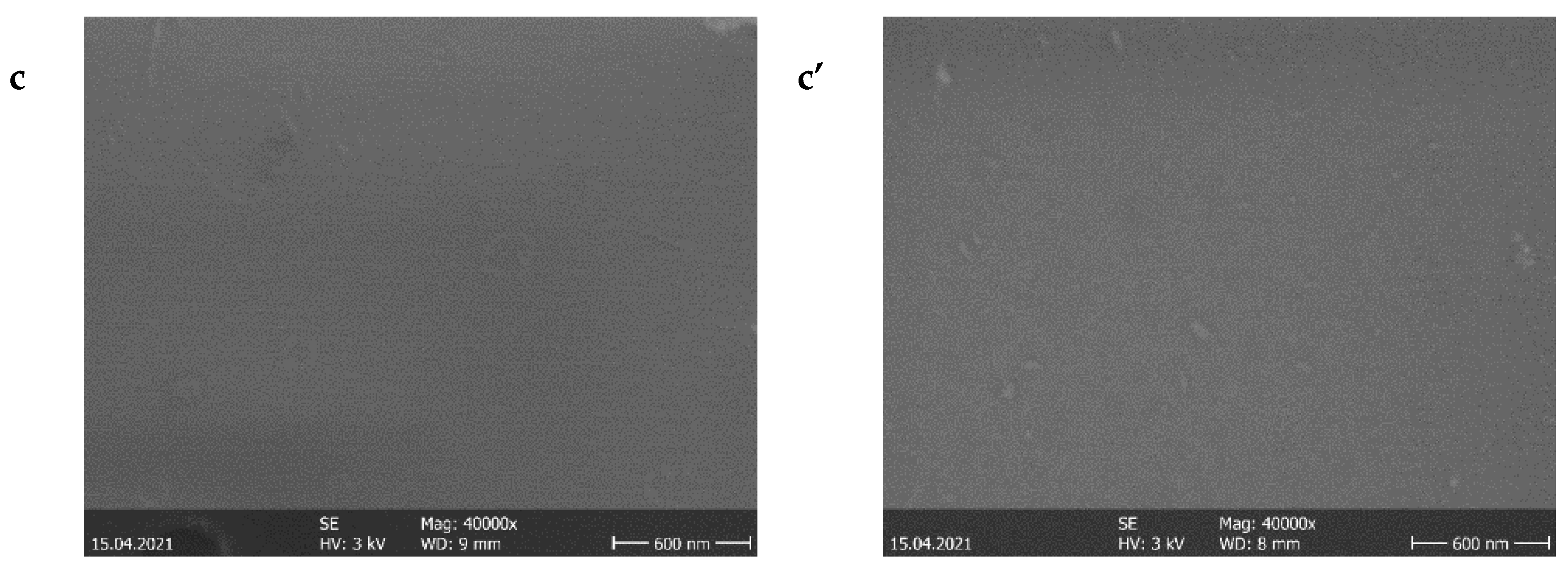
Figure 1a–c depicts the SEM micrographs of the bottom oxide films prior to the deposition of subsequent layers, and Figure 1a–c depicts the top of the second oxide layer of the three-layer structures (oxide/metal/oxide).
Figure 1.
SEM micrographs of single oxide (bottom) layers: (a) TiO2, (b) TiO2:Nb and (c) NiO; and SEM micrographs of the top oxide layers of oxide/Ag/oxide multilayer structures: (a’) TiO2, (b’) TiO2:Nb and (c’) NiO.
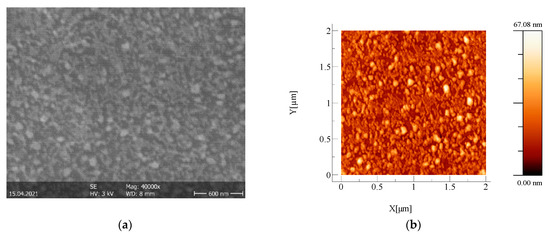
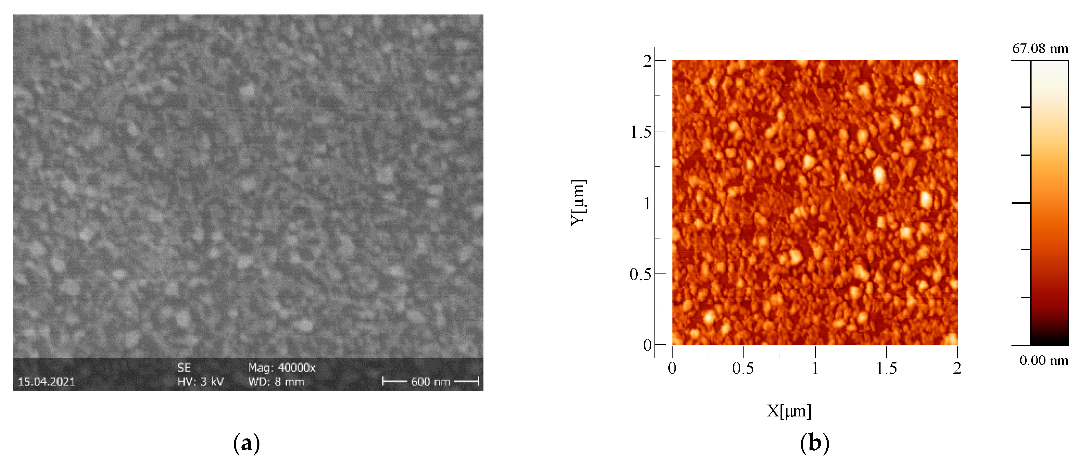
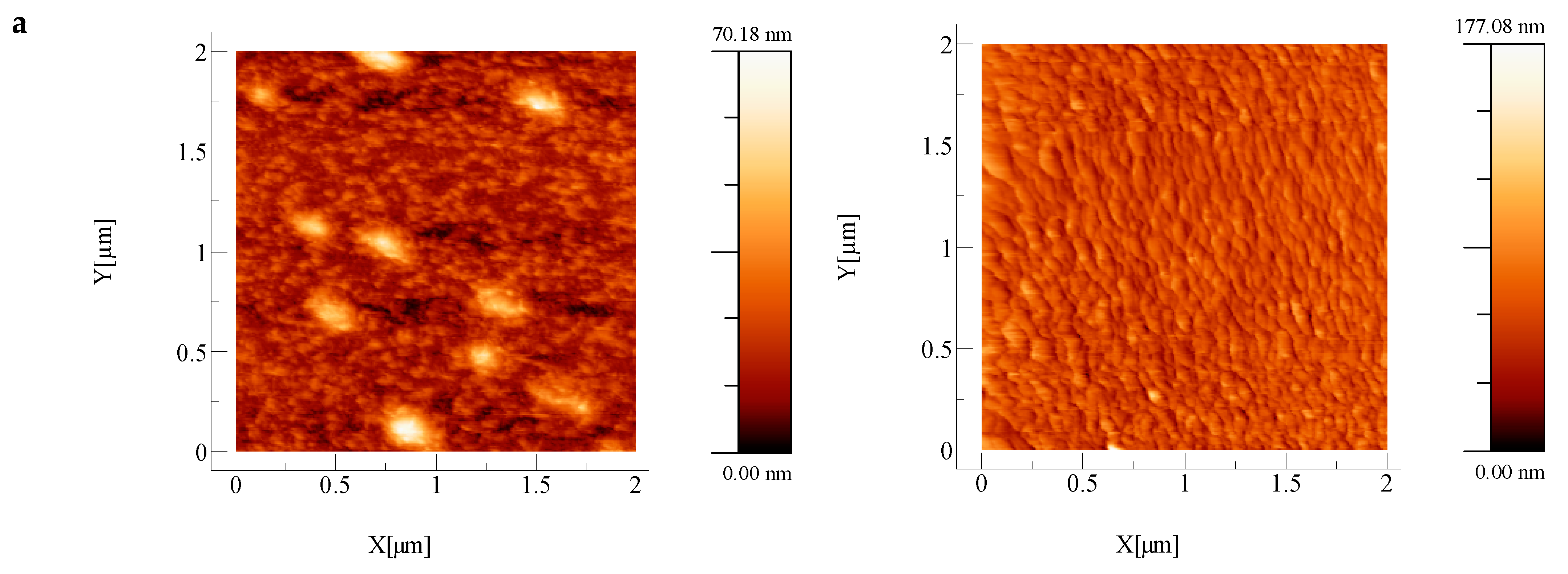
Figure 2 illustrates the SEM and AFM images of the silver interlayer. The AFM analysis was done both for the surfaces of the oxide single layers deposited on glass (not shown here) and for the top oxide layers of the oxide/metal/oxide multilayer structures deposited on glass. The root mean square (RMS) and average (RA) roughness values of these layers are given in Table 2.
Figure 2.
(a). SEM image of the Ag interlayer and (b) AFM image of the Ag interlayer.
Table 2.
A summary of RMS and RA roughness values, and contact angle (CA) values of the single oxide layers and the top oxide layers of the multilayer structures (O/M/O) deposited on glass and PET substrates.
Regarding the topography and morphological properties, the SEM micrographs show that the silver layer influenced the surface morphologies of the top surfaces of the O/M/O structures with TiO2 and TiO2:Nb, but this influence was smaller for the NiO-based structure. This can be explained, on the one hand, by the fact that the thickness of the NiO second layer was greater than those of the other two oxides (see Table 3), and on the other hand, by the fact that NiO’s roughness value was lower than those of TiO2 and TiO2:Nb layers.
Table 3.
Thicknesses obtained from ellipsometry simulations.
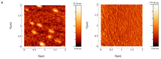
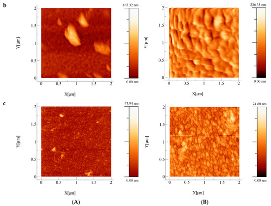
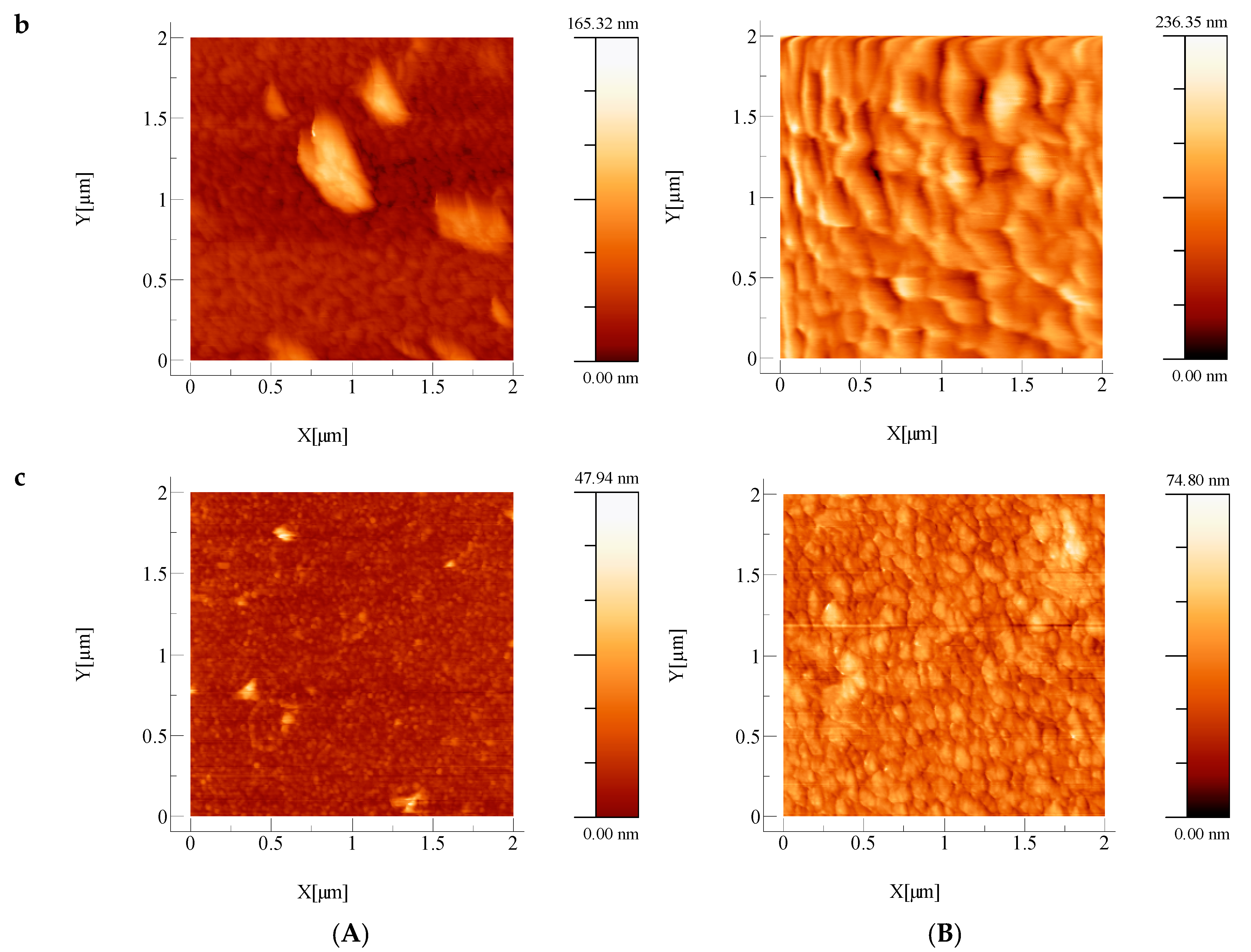
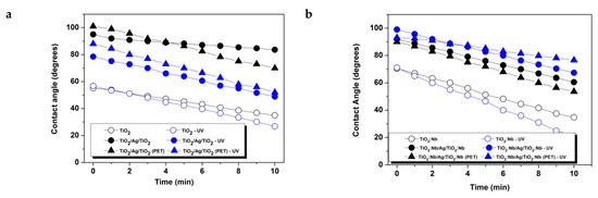
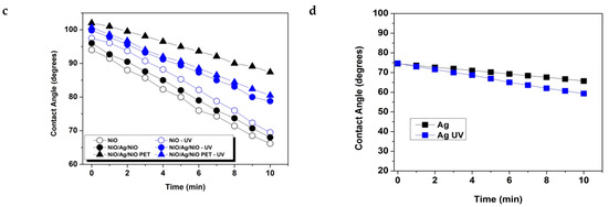
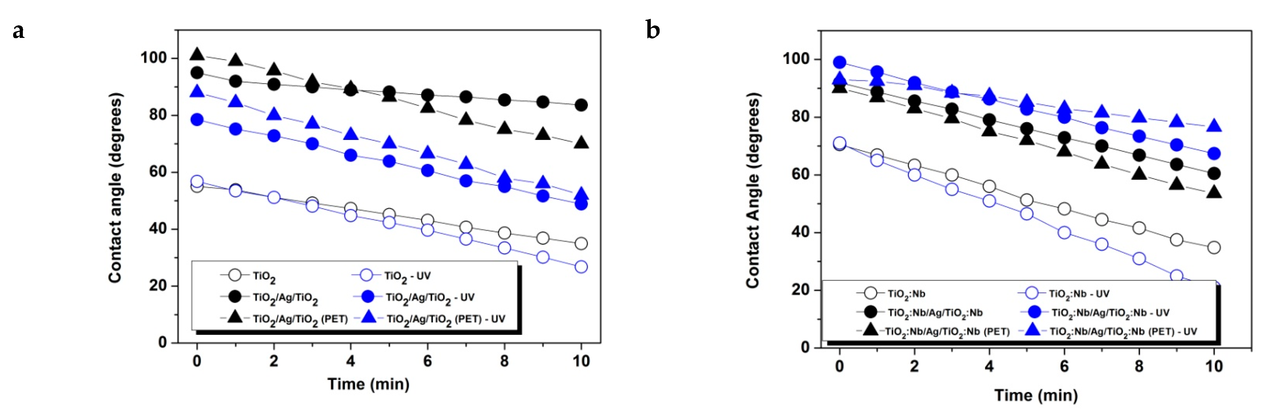
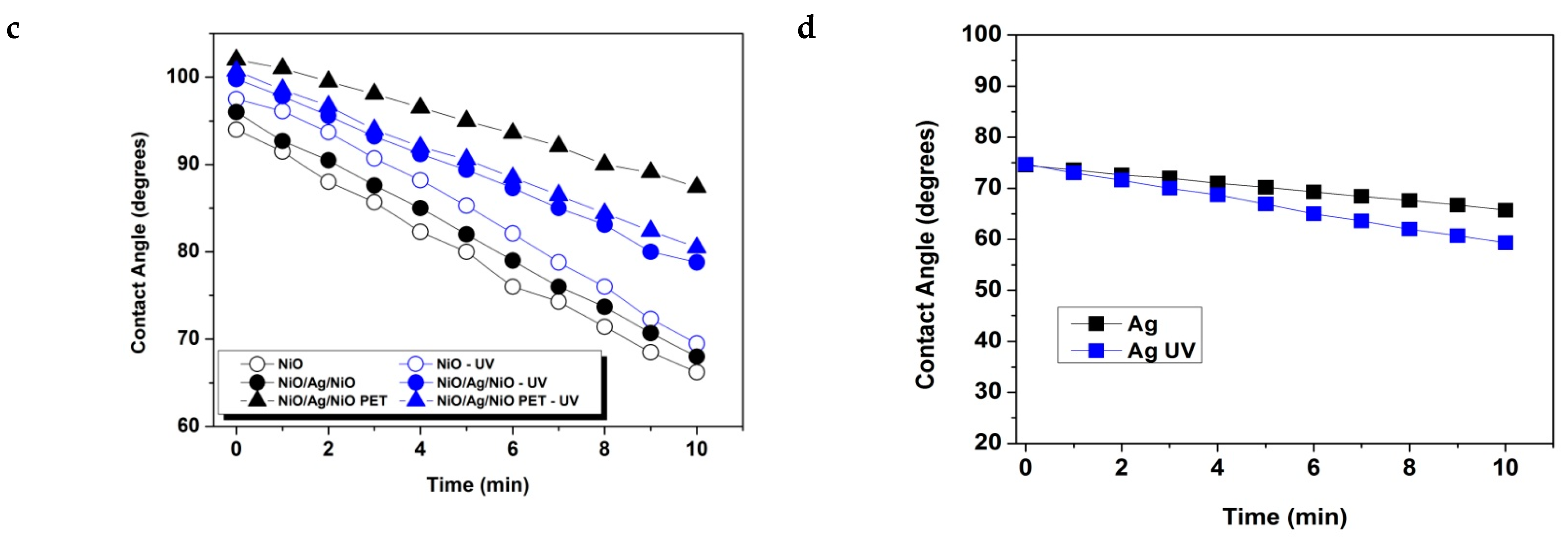
Figure 3 reproduces the AFM images obtained by scanning the top surfaces of the oxide/metal/oxide layers deposited on glass and on plastic substrates. As was the case for films of ITO/Metal/ITO, AZO/Metal/AZO and ZnO/Metal/ZnO studied previously [15], the films deposited on plastic substrates were rougher than the films deposited on glass substrates (see Table 2). Since the morphology in this context is closely related to wettability expressed in terms of contact angles, we measured such contact angles, and the results are given in Table 2. As one can see, the existence of the metallic interlayer increased the contact angle of the oxide surface in every case. All surfaces were also sensitive to UV exposure. The changes of the contact angles as a function of time with and without exposure to UV irradiation by using a 254 UV-C a 1 × 8W EF180C 1180 mW/cm2 lamp, are given in Figure 4. For TiO2 films and TiO2/Ag/TiO2 films on glass and plastic substrates, the contact angles decreased after exposure to UV, indicating that the surfaces became more hydrophilic. This is in agreement with the classical behavior of TiO2 films [36]. For TiO2:Nb/Ag/TiO2:Nb and NiO/Ag/NiO, the influence of UV radiation was quite slight.
Figure 3.
AFM analyses of top surfaces of oxide/Ag/oxide structures deposited on glass (A) and on PET (B): (a) TiO2/Ag/TiO2, (b) TiO2:Nb/Ag/TiO2:Nb and (c) NiO/Ag/NiO.
Figure 4.
Contact angle measurements with and without UV irradiation for single and three-layer samples: (a) TiO2; (b) TiO2:Nb; (c) Nio; (d) Ag interlayer.
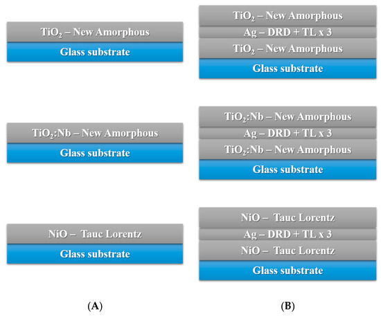
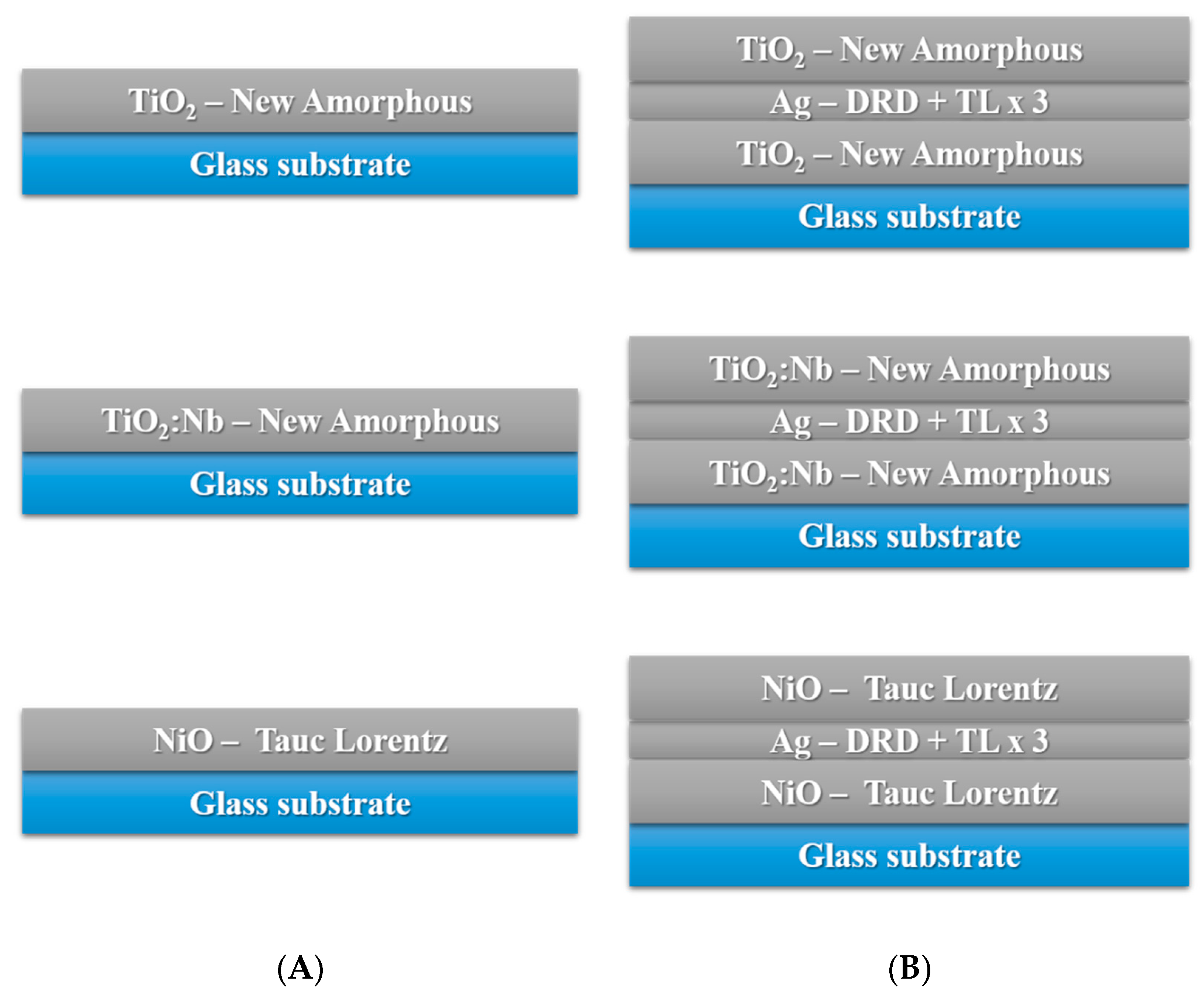
Refractive index and film thickness were determined by spectroscopic ellipsometry. Thickness for single layers and the individual thicknesses in multilayer structures were determined by fitting the experimental ellipsometric spectra with those which resulted from theoretical models. For the numerical simulations and modeling, we used the Delta Psi2 software from Horiba Jobin Yvon. The global refractive indices of structures were measured and modelled using the following dispersion formulas: the new amorphous dispersion formula for TiO2 and TiO2:Nb; the Tauc–Lorentz formula for NiO; and the Drude and Tauc–Lorentz formulae for Ag.
Figure 5 illustrates the optical models used for the theoretical calculations and simulations for single layers (A) and O/M/O structures (B).
Figure 5.
Ellipsometric models for single layers (A) and O/M/O three-layer structures (B).
The films’ thickness values obtained after the optimization of the models as described in [17], are given in Table 3.
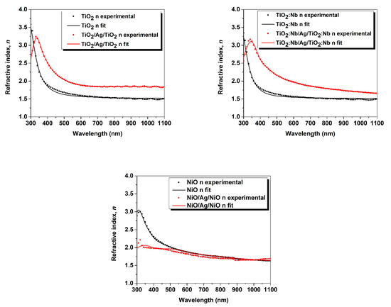
In Figure 6, the experimental ellipsometric data for the global refractive index are represented as dotted lines, and the fitting curves as continuous lines. The optimal thickness of the silver interlayer, realized by ellipsometric measurements (Table 3) is of 8 nm [20]. This thickness is the lowest limit because, for lower values, the film does not completely cover the substrate, and islands of Ag might appear which are not interconnected, making the resulting layer not conductive. By increasing the thickness, the metallic interlayer is certainly conductive, but the transparency of the O/M/O electrode is reduced.
Figure 6.
Ellipsometry experimental data (dotted lines) fitted by theoretically calculated curves (continuous lines) from the ellipsometric models, for single and three-layer samples.
As for single-layer films deposited by a sol–gel method—or in this case for films deposited by reactive sputtering—the refractive indices of thin Nb-doped TiO2 films are smaller than those of an undoped TiO2 thin films [37]. For the multilayer structures TiO2/Ag/TiO2 and TiO2:Nb/Ag/TiO2:Nb, the refractive indices were higher than those of single layers. On the contrary, the refractive index of NiO/Ag/NiO was smaller than the refractive index of the NiO single layer. These optical properties are important, since these films are used as electrodes for solar cells and optoelectronic devices.
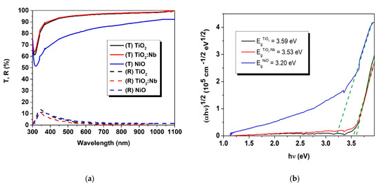
The transmittance and reflectance spectra for single layers, obtained by spectrophotometry, are given in Figure 7a. From these spectra, the optical energy band gaps were calculated using the Tauc plots (Figure 7b) for indirect optical transitions. The calculated band gap values were compared with the results from the ellipsometric modelling and those given in literature (see Table 4). We can report a satisfactory correlation between the values obtained by different methods, and satisfactory correlations with those reported by others authors—this being the second verification of the validity of the ellipsometric optical models.
Figure 7.
(a) Transmittance and reflectance spectra for the single-layer coatings; (b) energy band gap calculation using spectrophotometry data.
Table 4.
Energy band gap values from spectrophotometric and ellipsometric measurements.
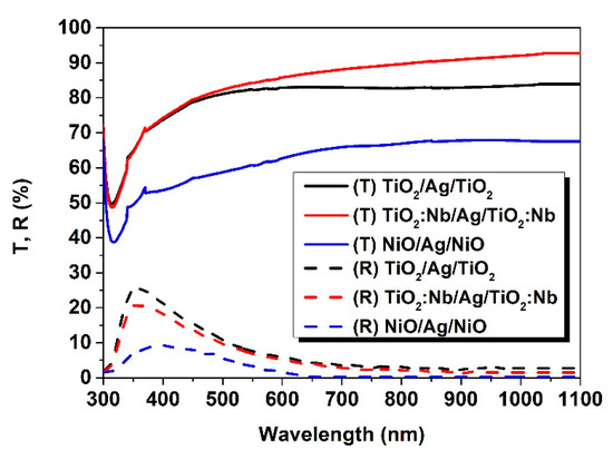
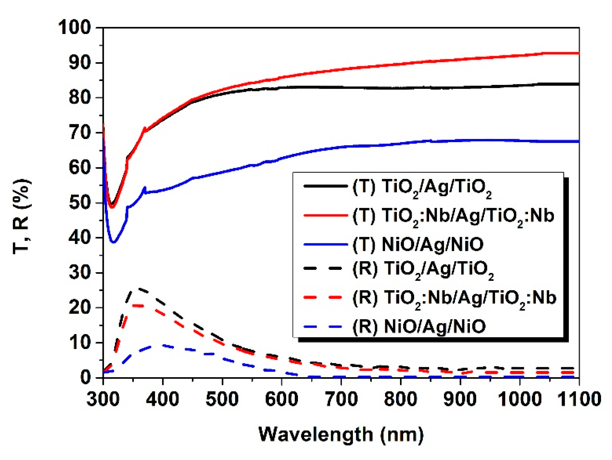
Similarly to Figure 7, Figure 8 gives the transmittance and reflectance spectra for O/M/O layers. Due to the increased thicknesses of these structures, the transmittance was 10% lower.
Figure 8.
Transmittance and reflectance spectra for the O/M/O structures by spectrophotometry.
Due to the presence of the Ag interlayer, the reflectance increased consistently by 10%, except for the NiO/Ag/NiO three-layer structure, for which the optical features of silver were reduced by the thicker NiO top layer.
The electrical resistivity values determined from direct measurements and also from ellipsometric calculations were roughly 7 × 10⁻³ Ω∙cm for TiO2/Ag/TiO2, 1 × 10⁻⁴ Ω∙cm for TiO2:Nb/Ag/TiO2:Nb and 2 × 10⁻⁴ Ω∙cm for NiO/Ag/NiO, and are in line with the values obtained by other authors [32,33,35,40] for films deposited on oxide targets. The correlation between the electrical measurements and the ellipsometric simulations is demonstrated by equivalent values of plasma frequency. Therefore, taking into account Drude’s model describing the kinetic theory of electrons in metal, plasma frequency is defined as follows [39]:
where σ represents the electrical conductivity; is the vacuum permittivity ( generally, according to the Lorentz dispersion model, on which Drude’s model is based; and is the relaxation time of electrons (for Ag electrons, [40,41]).
The resulting values of plasma frequency based on electrical conductivity (from direct measurements) are compared with the values of plasma frequency released in the ellipsometric simulations of samples in Table 5.
Table 5.
A comparison between plasma frequency values obtained from direct electrical measurements and from ellipsometric simulations.
The differences in the values of plasma frequency calculated from electrical measurements and from ellipsometric modelling are within reasonable limits when taking into account the fact that the spectroscopic ellipsometry technique is based on reflections at one point (local measurements) and also taking into account the limits in the accuracy of the models.
By analyzing all these data, we can conclude that TiO2/Ag/TiO2, TiO2:Nb/Ag/TiO2:Nb and NiO/Ag/NiO have quite similar optical and electrical properties. However, higher values of transparency and electrical conductivity were obtained for TiO2:Nb/Ag/TiO2:Nb. The NiO/Ag/NiO three-layer electrodes could be slightly improved by reducing the oxide layer’s thickness. The main advantage of NiO/Ag/NiO electrodes is the fact that the refractive index is lower than those of TiO2/Ag/TiO2 and TiO2:Nb/Ag/TiO2:Nb. Using ellipsometry, which is a powerful tool, the established optimal models will be used in a future work to simulate the properties of the new optimized structure.
4. Conclusions
We presented a comparative study regarding the physical properties of oxide/metal/oxide three-layer structures which are promising alternatives to ITO electrodes in the photovoltaic field. The oxide layers (TiO2, TiO2:Nb, NiO) and the metallic interlayer (Ag) were laid by successive DC sputtering deposition on glass and plastic substrates. The performances of this type of electrode architecture were presented from optical and electrical points of view, and we also described the morphological features. The presence of Ag as an interlayer influences the three-layer structure. Firstly, the transmittance shows a decrease of 10%, and the reflectance an increase of 10%, the latter depending on the oxide layer’s thickness. Secondly, the roughness of such a structure is directly dependent on the substrate roughness, and it too is influenced by the silver’s morphological properties. Thirdly, from an electrical point of view, in terms of electrical resistivity (~10−3 Ω∙cm), these O/M/O structures presented huge potential for photovoltaic applications as transparent conductive electrodes. The ellipsometry optical models were validated by combining different direct measurements. These ellipsometric models can be now used to simulate the properties of new optimized structures.
Author Contributions
Conceptualization, M.G.; methodology, L.H., M.G. and R.M.; software, L.H. and M.G.; validation, M.G. and L.L.; formal analysis, L.H. and M.G.; investigation, L.H., R.M. and M.G.; resources, P.L., R.M. and M.G.; data curation, L.H. and M.G.; writing—original draft preparation, M.G. and L.H.; writing—review and editing, L.H., M.G. and L.L.; visualization, M.G.; supervision, M.G.; project administration, M.G.; funding acquisition, M.G. All authors have read and agreed to the published version of the manuscript.
Funding
The APC was funded by the European Social Fund, through Operational Programme Human Capital 2014–2020, project number POCU/380/6/13/123623, project title “PhD Students and Postdoctoral Researchers Prepared for the Labour Market”.
Institutional Review Board Statement
Not applicable.
Informed Consent Statement
Not applicable.
Acknowledgments
The authors are grateful to SCIAM—Microscopy Service, for AFM and SEM micrographs, to N. Mercier and Magali Alain from Moltech Laboratory for providing the necessary facilities for XRD studies and to M. Vieira for technical support.
Conflicts of Interest
The authors declare no conflict of interest.
References
- Loka, C.; Moon, S.W.; Choi, Y.; Lee, K.-S. High Transparent and Conductive TiO2/Ag/TiO2 Multilayer Electrode Films Deposited on Sapphire Substrate. Electron. Mater. Lett. 2018, 14, 125–132. [Google Scholar] [CrossRef] [Scilit]
- Girtan, M.; Wittenberg, A.; Grilli, M.L.; de Oliveira, D.P.S.; Giosuè, C.; Ruello, M.L. The Critical Raw Materials Issue between Scarcity, Supply Risk, and Unique Properties. Materials 2021, 14, 1826. [Google Scholar] [CrossRef] [Scilit]
- Kim, B.-G.; Kim, J.-Y.; Lee, S.-J.; Park, J.-H.; Lim, D.-G.; Park, M.-G. Structural, Electrical and Optical Properties of Ga-Doped ZnO Films on PET Substrate. Appl. Surf. Sci. 2010, 257, 1063–1067. [Google Scholar] [CrossRef] [Scilit]
- Liu, C.C.; Wu, M.L.; Liu, K.C.; Hsiao, S.-H.; Chen, Y.S.; Lin, G.-R.; Huang, J. Transparent ZnO Thin-Film Transistors on Glass and Plastic Substrates Using Post-Sputtering Oxygen Passivation. J. Disp. Technol. 2009, 5, 192–197. [Google Scholar] [CrossRef] [Scilit]
- Jandow, N.N.; Yam, F.K.; Thahab, S.M.; Ibrahim, K.; Abu Hassan, H. The Characteristics of ZnO Deposited on PPC Plastic Substrate. Mater. Lett. 2010, 64, 2366–2368. [Google Scholar] [CrossRef] [Scilit]
- Banerjee, A.; Ghosh, C.; Chattopadhyay, K.; Minoura, H.; Sarkar, A.; Akiba, A.; Kamiya, A.; Endo, T. Low-Temperature Deposition of ZnO Thin Films on PET and Glass Substrates by DC-Sputtering Technique. Thin Solid Film. 2006, 496, 112–116. [Google Scholar] [CrossRef] [Scilit]
- Girtan, M.; Kompitsas, M.; Mallet, R.; Fasaki, I. On Physical Properties of Undoped and Al and In Doped Zinc Oxide Films Deposited on PET Substrates by Reactive Pulsed Laser Deposition. Eur. Phys. J. Appl. Phys. 2010, 51. [Google Scholar] [CrossRef] [Scilit]
- Girtan, M.; Rusu, G.G.; Dabos-Seignon, S.; Rusu, M. Structural and Electrical Properties of Zinc Oxides Thin Films Prepared by Thermal Oxidation. Appl. Surf. Sci. 2008, 254, 4179–4185. [Google Scholar] [CrossRef] [Scilit]
- Rusu, M.; Rusu, G.G.; Girtan, M.; Seignon, S.D. Structural and Optical Properties of ZnO Thin Films Deposited onto ITO/Glass Substrates. J. Non-Cryst. Solids 2008, 354, 4461–4464. [Google Scholar] [CrossRef] [Scilit]
- Ghomrani, F.-Z.; Iftimie, S.; Gabouze, N.; Serier, A.; Socol, M.; Stanculescu, A.; Sanchez, F.; Antohe, S.; Girtan, M. Influence of Al Doping Agents Nature on the Physical Properties of Al:ZnO Films Deposited by Spin-Coating Technique. Optoelectron. Adv. Mater. Rapid Commun. 2011, 5, 247–251. [Google Scholar]
- Girtan, M.; Bouteville, A.; Rusu, G.; Rusu, M. Preparation and Properties of SnO2: F Thin Films. J. Optoelectron. Adv. Mater. 2006, 8, 27–30. [Google Scholar]
- Fortunato, E.; Raniero, L.; Silva, L.; Goncalves, A.; Pimentel, A.; Barquinha, P.; Aguas, H.; Pereira, L.; Goncalves, G.; Ferreira, I.; et al. Highly Stable Transparent and Conducting Gallium-Doped Zinc Oxide Thin Films for Photovoltaic Applications. Sol. Energy Mater. Sol. Cells 2008, 92, 1605–1610. [Google Scholar] [CrossRef] [Scilit]
- Fortunato, E.; Goncalves, A.; Pimentel, A.; Barquinha, P.; Goncalves, G.; Pereira, L.; Ferreira, I.; Martins, R. Zinc Oxide, a Multifunctional Material: From Material to Device Applications. Appl. Phys. A Mater. Sci. Process. 2009, 96, 197–205. [Google Scholar] [CrossRef] [Scilit]
- Socol, M.; Preda, N.; Breazu, C.; Florica, C.; Costas, A.; Istrate, C.M.; Stanculescu, A.; Girtan, M.; Gherendi, F. Organic Heterostructures Obtained on ZnO/Ag/ZnO Electrode. Vacuum 2018, 154, 366–370. [Google Scholar] [CrossRef] [Scilit]
- Girtan, M. Comparison of ITO/Metal/ITO and ZnO/Metal/ZnO Characteristics as Transparent Electrodes for Third Generation Solar Cells. Sol. Energy Mater. Sol. Cells 2012, 100, 153–161. [Google Scholar] [CrossRef] [Scilit]
- Hrostea, L.; Boclinca, M.; Socol, M.; Leontie, L.; Stanculescu, A.; Girtan, M. Oxide/Metal/Oxide Electrodes for Solar Cell Applications. Sol. Energy 2017, 146, 464–469. [Google Scholar] [CrossRef] [Scilit]
- Girtan, M.; Hrostea, L.; Boclinca, M.; Negulescu, B. Study of Oxide/Metal/Oxide Thin Films for Transparent Electronics and Solar Cells Applications by Spectroscopic Ellipsometry. AIMS Mater. Sci. 2017, 4, 594–613. [Google Scholar] [CrossRef] [Scilit]
- Antohe, S.; Iftimie, S.; Hrostea, L.; Antohe, V.A.; Girtan, M. A Critical Review of Photovoltaic Cells Based on Organic Monomeric and Polymeric Thin Film Heterojunctions. Thin Solid Film. 2017, 642, 219–231. [Google Scholar] [CrossRef] [Scilit]
- Socol, M.; Preda, N.; Breazu, C.; Stanculescu, A.; Costas, A.; Stanculescu, F.; Girtan, M.; Gherendi, F.; Popescu-Pelin, G.; Socol, G. Flexible Organic Heterostructures Obtained by MAPLE. Appl. Phys. A Mater. Sci. Process. 2018, 124, 602. [Google Scholar] [CrossRef] [Scilit]
- Dhar, A.; Alford, T.L. High Quality Transparent TiO2/Ag/TiO2 Composite Electrode Films Deposited on Flexible Substrate at Room Temperature by Sputtering. APL Mater. 2013, 1, 012102. [Google Scholar] [CrossRef] [Scilit]
- Kim, J.H.; Kim, D.-H.; Seong, T.-Y. Realization of Highly Transparent and Low Resistance TiO2/Ag/TiO2 Conducting Electrode for Optoelectronic Devices. Ceram. Int. 2015, 41, 3064–3068. [Google Scholar] [CrossRef] [Scilit]
- Ji, L.-W.; Hsiao, Y.-J.; Young, S.-J.; Shih, W.-S.; Water, W.; Lin, S.-M. High-Efficient Ultraviolet Photodetectors Based on TiO2/Ag/TiO2 Multilayer Films. IEEE Sens. J. 2015, 15, 762–765. [Google Scholar] [CrossRef] [Scilit]
- Kim, K.-D.; Pfadler, T.; Zimmermann, E.; Feng, Y.; Dorman, J.A.; Weickert, J.; Schmidt-Mende, L. Decoupling Optical and Electronic Optimization of Organic Solar Cells Using High-Performance Temperature-Stable TiO2/Ag/TiO2 Electrodes. APL Mater. 2015, 3. [Google Scholar] [CrossRef] [Scilit]
- Zhu, M.-Q.; Jin, H.-D.; Bi, P.-Q.; Zong, F.-J.; Ma, J.; Hao, X.-T. Performance Improvement of TiO2/Ag/TiO2 Multilayer Transparent Conducting Electrode Films for Application on Photodetectors. J. Phys. D Appl. Phys. 2016, 49, 115108. [Google Scholar] [CrossRef] [Scilit]
- Jia, J.H.; Zhou, P.; Xie, H.; You, H.Y.; Li, J.; Chen, L.Y. Study of Optical and Electrical Properties of TiO2/Ag/TiO2 Multilayers. J. Korean Phys. Soc. 2004, 44, 717–721. [Google Scholar]
- Baskoutas, S.; Athanasiou, N. Optical Constants of TiO2/Ag/TiO2 Three-Layer Thin Films. Mod. Phys. Lett. B 1997, 11, 1077–1084. [Google Scholar] [CrossRef] [Scilit]
- Hasan, M.M.; Haseeb, A.; Saidur, R.; Masjuki, H.H.; Johan, M.R. Structural, Optical and Morphological Properties of TiO 2/Ag/TiO2 Multilayer Films. In AIP Conference Proceedings; American Institute of Physics: College Park, MD, USA, 2009; Volume 1136, pp. 229–233. [Google Scholar]
- Zhao, Z.; Alford, T.L. The Optimal TiO2/Ag/TiO2 Electrode for Organic Solar Cell Application with High Device-Specific Haacke Figure of Merit. Sol. Energy Mater. Sol. Cells 2016, 157, 599–603. [Google Scholar] [CrossRef] [Scilit]
- Zhao, Z.; Alford, T.L. The Effect of Hole Transfer Layers and Anodes on Indium-Free TiO2/Ag/TiO2 Electrode and ITO Electrode Based P3HT:PCBM Organic Solar Cells. Sol. Energy Mater. Sol. Cells 2018, 176, 324–330. [Google Scholar] [CrossRef] [Scilit]
- Varnamkhasti, M.G.; Shahriari, E. Design and Fabrication of Nanometric TiO2/Ag/TiO2/Ag/TiO2 Transparent Conductive Electrode for Inverted Organic Photovoltaic Cells Application. Superlattices Microstruct. 2014, 69, 231–238. [Google Scholar] [CrossRef] [Scilit]
- Singh, S.; Sharma, V.; Asokan, K.; Sachdev, K. NTO/Ag/NTO Multilayer Transparent Conducting Electrodes for Photovoltaic Applications Tuned by Low Energy Ion Implantation. Sol. Energy 2018, 173, 651–664. [Google Scholar] [CrossRef] [Scilit]
- Park, J.-H.; Kim, H.-K.; Lee, H.; Lee, H.; Yoon, S.; Kim, C.-D. Highly Transparent, Low Resistance, and Cost-Efficient Nb:TiO2/Ag/Nb:TiO2 Multilayer Electrode Prepared at Room Temperature Using Black Nb:TiO2 Target. Electrochem. Solid State Lett. 2010, 13, J53–J56. [Google Scholar] [CrossRef] [Scilit]
- Mardare, D.; Yildiz, A.; Girtan, M.; Manole, A.; Dobromir, M.; Irimia, M.; Adomnitei, C.; Cornei, N.; Luca, D. Surface Wettability of Titania Thin Films with Increasing Nb Content. J. Appl. Phys. 2012, 112. [Google Scholar] [CrossRef] [Scilit]
- Manole, A.V.; Dobromir, M.; Girtan, M.; Mallet, R.; Rusu, G.; Luca, D. Optical Properties of Nb-Doped TiO2 Thin Films Prepared by Sol-Gel Method. Ceram. Int. 2013, 39, 4771–4776. [Google Scholar] [CrossRef] [Scilit]
- Li, H.; Chen, C.; Jin, J.; Bi, W.; Zhang, B.; Chen, X.; Xu, L.; Liu, D.; Dai, Q.; Song, H. Near-Infrared and Ultraviolet to Visible Photon Conversion for Full Spectrum Response Perovskite Solar Cells. Nano Energy 2018, 50, 699–709. [Google Scholar] [CrossRef] [Scilit]
- Chang, K.-C.; Yeh, T.-H.; Lee, H.-Y.; Lee, C.-T. High Performance Perovskite Solar Cells Using Multiple Hole Transport Layer and Modulated FA(x)MA(1-x)PbI(3) Active Layer. J. Mater. Sci. Mater. Electron. 2020, 31, 4135–4141. [Google Scholar] [CrossRef] [Scilit]
- Xue, Z.; Liu, X.; Zhang, N.; Chen, H.; Zheng, X.; Wang, H.; Guo, X. High-Performance NiO/Ag/NiO Transparent Electrodes for Flexible Organic Photovoltaic Cells. Acs Appl. Mater. Interfaces 2014, 6, 16403–16408. [Google Scholar] [CrossRef] [Scilit] [PubMed]
- Hosny, N.M. Synthesis, Characterization and Optical Band Gap of NiO Nanoparticles Derived from Anthranilic Acid Precursors via a Thermal Decomposition Route. Polyhedron 2011, 30, 470–476. [Google Scholar] [CrossRef] [Scilit]
- Ashcroft, N.W.; Mermin, N.D. Solid State Physics; Holt, Rinehart & Winston: New York, NY, USA; London, UK, 1976; Volume 2005. [Google Scholar]
- Ramanathan, K.G.; Yen, S.H.; Estalote, E.A. Total Hemispherical Emissivities of Copper, Aluminum, and Silver. Appl. Opt. 1977, 16, 2810–2817. [Google Scholar] [CrossRef] [Scilit]
- Yang, H.U.; D’Archangel, J.; Sundheimer, M.L.; Tucker, E.; Boreman, G.D.; Raschke, M.B. Optical Dielectric Function of Silver. Phys. Rev. B 2015, 91, 235137. [Google Scholar] [CrossRef] [Scilit]

Publisher’s Note: MDPI stays neutral with regard to jurisdictional claims in published maps and institutional affiliations. |
© 2021 by the authors. Licensee MDPI, Basel, Switzerland. This article is an open access article distributed under the terms and conditions of the Creative Commons Attribution (CC BY) license (https://creativecommons.org/licenses/by/4.0/).