


Abstract
The current trend of globalization of the supply chain in the integrated circuit (IC) industry has led to numerous security issues, such as intellectual property (IP) piracy, overbuilding, hardware Trojan (HT), and so on. Over the past decade or so, logic locking has been developed as an important method to prevent or mitigate the above security issues in ICs throughout their lifecycles. However, most published logic locking schemes are vulnerable to the SAT attack and its variants. Existing SAT-resilient locking schemes always entail a trade-off between security and effectiveness and incur significant hardware overhead. In this paper, we propose a new replacement-based key-controlled circuit (called RKC), the application of which changes the underlying framework of traditional logic locking designs, making the SAT attack and its variants infeasible in the framework. To achieve stronger functional and structural obfuscation and to validate the extensibility of the proposed method within the modified logic-locking design framework, we develop a new multi-input key-controlled circuit (called MKC) via vertical extension, also based on replacement applied to the locking design. In addition, we expand the two proposed circuits horizontally by varying the design parameter m, yielding four logic-locking design circuits. Relevant experiments performed on six selected benchmark circuits from ISCAS’85 and MCNC benchmarks show that the proposed method demonstrates superior/less hardware overhead compared to four recently published locking methods, i.e., GateLock, SKG-Lock, SKG-Lock+, and CAS-Lock.
1. Introduction
Integrated circuits (ICs) are the backbone of modern computing systems. Today’s ICs are produced in a diversified global supply chain, where multiparty means that multiple countries or regions design, validate, and manufacture a particular integrated circuit. According to the 2023 Update by the Semiconductor Industry Association (SIA), direct losses to the IC industry due to hardware security threats arising from globalization of the IC supply chain are estimated to be between $60 billion and $75 billion annually. Therefore, circuit safety has attracted extensive attention in the IC field in the last decade. One of the most discussed issues is untrustworthy foundries, which threaten circuit security in mainly three ways: (1) maliciously modifying circuit designs, (2) obtaining critical information through reverse engineering to help develop or steal intellectual property (IP), and (3) illegally cloning, copying, or overproducing circuit designs [1].
While measures such as policy development, market regulation, and intellectual property enforcement can help deter these threats, design-based or manufacture-based techniques can provide a more cost-effective solution. Most IC supply chain threats primarily stem from circuit designs being leaked to malicious actors, thus hiding or obfuscating the design can impede such attacks. Logic locking is an important technique for preventing attackers from threatening the security of circuits, which does not require a trustworthy foundry and can be achieved by modifying the circuit design and, in some cases, with only minor modifications to the manufacturing process [1].
Conventional logic locking modifies the design circuit to be protected by locking the original design using key input bits, and the resulting protected design circuit is referred to as a locked design. The conventional logic locking design framework is shown in Figure 1a, which has two types of inputs: primary inputs and key inputs. A locked design is functionally equivalent to the original design only if the correct key is applied to the key input [2,3,4]. The correct key is stored in secure tamper-proof memory after manufacturing, and its contents cannot be accessed or tampered with outside of the chip. The locking process takes place in the trusted design room. The locked design is returned to the designer or remotely accessed via the secure key exchange protocol for loading the correct key to obtain the activated circuit after it has undergone manufacturing and testing at the untrustworthy foundry. Without the correct key, attackers have no access to the original design, so logic locking can effectively protect IP security by preventing attackers from reverse engineering or overproducing circuit designs.
Figure 1.
Conventional and modified logic locking design frameworks. (a) Conventional logic locking design framework. (b) Modified logic locking design framework.
However, the SAT attack [2], a highly powerful and strongly extensible attack method, has changed the development direction of logic locking. To date, the SAT attack remains a significant attack that threatens the security of logic locking. In addition, K. Shamsi et al. [5] and Y. Shen et al. [6] proposed two new attacks, AppSAT and Double-DIP, respectively, which are variants of the SAT attack. Compared to the SAT attack, the AppSAT and Double-DIP attacks terminate early to return an approximation key, thus obtaining an approximation of the unlocked netlist. The main difference between these two attacks lies in the distinct conditions for early termination: when error estimation is performed after every d queries of the distinguishing input pattern, AppSAT terminates the attack when the obtained error estimates are consistently below the threshold for more than the number of settlements, and Double-DIP terminates the attack when no more 2-DIPs can be found that eliminate at least two incorrect keys.
Before the SAT attack was published, four main logic locking techniques were introduced in the field of hardware security, namely RLL [7,8], LUT [9], SLL [10,11], and FLL [12]. Where, RLL [7,8], locks the design by inserting XOR/XNOR gates at k random locations in the original netlist and changes the single mapping relationship between the key gate type (XOR/XNOR) and the correct key value (0/1) by the bubble push method. LUT [9] uses the look-up table (LUT) as a reconfigurable logic barrier, and the LUT stores the correct key as its contents to lock the design. When the LUT storage content is correctly programmed, the circuit information in the locked design propagates correctly according to the circuit information in the original design; conversely, incorrectly programmed LUT storage content will result in erroneous propagation of the circuit information, which will lead to incorrectly outputs. SLL [10,11] achieves strong logic locking by ensuring an inter-dependence between key gates in the circuit topology, and this locking technique provides favorable security against the sensitization attack [10]. FLL [12] achieves the locking goal of an error key being able to affect the 50% (ideally) output of any input pattern by inserting a key gate (XOR/XNOR/MUX) at the location with the maximum fault impact.
Unfortunately, none of the four logic-locking techniques above are resistant to the SAT attack, which is why we consider the SAT attack to have changed the direction of logic locking. To tackle this challenge, researchers have developed a series of logic locking schemes with high security against the subject of the SAT attack resilience. SARLock [13] employs a small comparator circuit to generate a flipping signal from specific circuit inputs and key combinations. A mask logic is inserted to block the flipping output under the correct key. Its extremely low output corruption causes the number of iterations and iteration time required by the SAT attack to increase exponentially. Anti-SAT [14] employs a parallel dual-AND-tree architecture, wherein the second AND tree’s output is inverted and combined with the first AND tree to form a locking logic that incorporates both the flipping signal and the correct key. For Anti-SAT, the number of iterations required for the SAT attack is , thereby achieving SAT resilience. SFLL-HD [3] introduces the concept of Hamming distance between the circuit inputs and key inputs, structurally composed of a stripped-functionality circuit and a restore unit. The stripped-functionality circuit modifies the original design to invert the output of input cubes with a Hamming distance of h from the correct key under each input key. The restore unit then inverts the output when the Hamming distance between the circuit inputs and key inputs is h, thereby eliminating built-in errors and restoring the correct output. While these locking schemes enhance security against the SAT attack, they also exhibit notable design flaws. They often require integration with other logic-locking techniques to improve resistance to other attacks. The compound schemes [1] formed thus involve a trade-off between area overhead and anti-attack capability.
This paper addresses a critical research question: Whether existing logic locking techniques effectively defend against the SAT attack and its variants while significantly reducing hardware overhead? To address this question, the paper presents the following main contributions:
(1) We propose a new replacement-based key-controlled circuit (called RKC) based on constructing the relevant constraint relationship between the key inputs and the design gate inputs. The application of this circuit changes the underlying framework of traditional logic-locking designs, rendering the SAT attack and its variants infeasible within that framework.
(2) In order to achieve stronger functional obfuscation and structural obfuscation as well as to validate the extensibility of the proposed approach/replacement-based key-controlled circuit in the modified logic locking design framework, we propose a new multi-input key-controlled circuit (called MKC) by vertical expansion, which is also applied to the locking design in a replacement-based manner.
(3) We expand the above two proposed circuits horizontally by modifying the value of the design parameter m, obtaining four logic locking design circuits. Experimental results on six benchmark circuits from ISCAS’85 and MCNC show that the proposed method incurs less additional hardware overhead than the four recently published locking methods: GateLock, SKG-Lock, SKG-Lock+, and CAS-Lock.
(4) In addition, we have separately analyzed the additional hardware overhead produced by each locking circuit in the proposed method. Compared to the locking circuits of each logic gate in GateLock, each locking circuit in the proposed method demonstrates superior/less hardware overhead.
The rest of the paper is organized as follows. Section 2 reviews various SAT resilient logic locking techniques proposed/developed after the emergence of the SAT attack and their vulnerability to other novel attacks. Section 3 introduces the relevant preliminary knowledge that underpins the overall framework and the design idea of the proposed method. Section 4 details the specific implementation of the replacement-based key-controlled circuits (RKC), the multi-input key-controlled circuits (MKC), and their related extensions, the security analysis of the proposed method, and its differentiation from GateLock. Section 5 shows the performance evaluation experiments and comparative analysis results of the proposed method. Section 6 summarizes the paper.
2. Related Work
In the past decade, researchers have successively proposed a series of SAT-resilient logic locking techniques, which can be categorized into five main classes according to the different locking mechanisms: point function-based logic locking, stripped-functionality logic locking, fault analysis-based logic locking, cyclic logic locking, and one-way function-based logic locking.
Among the point function-based logic locking techniques, SARLock [13], Anti-SAT [14], and ATD [15] all control the identification ability of DIPs by the SAT attack through the point function constructed with the AND tree, where each DIP can only exclude one wrong key, which no doubt puts the SAT attack in the worst situation. SAS [16] serves as a variant of Anti-SAT, which inherits the complementary structure of Anti-SAT and builds the locking circuit to induce application-level errors by introducing the concept of critical minterms. As an extension of the point function-based logic locking, DTL [1] attains a higher onset size value by systematically using NAND/OR/XOR gates to replace selected gates in the AND tree, and the realization of this design goal can be used to resist the AppSAT attack. However, none of the above-mentioned logic locking techniques are resistant to at least one removal attack, such as signal probability skew (SPS) attack [17], AppSAT guided removal (AGR) attack [18], sensitization guided SAT (SGS) attack [18], and so on, due to their unique and distinct design features.
Unlike the removal attack, the bypass attack [19] uses two copies of the locked circuit to construct a mitered circuit, which is then fed to a SAT solver to perform operations to collect DIPs, and restores the normal functionality of the locked circuit in the presence of an erroneous key applied by utilizing these DIPs to construct a bypass circuit and stitching it into the locked circuit. SARLock, Anti-SAT is insecure against the bypass attack due to its extremely low output corruption. The proposed CAS-Lock [20] demonstrates its favorable SAT resilience and bypass resilience, but it is insecure against the removal attack; while M-CAS, as an extension of CAS-Lock, provides security against the removal attack but requires more hardware overhead as well.
The earliest of the stripped-functionality logic-locking techniques proposed is TTLock [21], which is a locking scheme that constructs stripped-functionality circuits by flipping the outputs for a single specific input pattern. SFLL-HD [3] and SFLL-flex [3] are extensions of TTLock, where SFLL-HD maintains the same Hamming distance value h from the correct key for all protected input patterns, and SFLL-flex is more flexible in that the designer/user can specify critical protected input patterns. For TTLock, due to its extremely low output corruption, it is vulnerable to the AppSAT attack [5] and the bypass attack [19]; for SFLL, due to the structural traces left by traditional security-agnostic synthesis tools, it is vulnerable to the FALL attack [22], the bit-coloring attack [23], and the structural analysis attack [24].
In the fault analysis-based logic locking techniques, the security of circuits relies on controllable faults regulated by keys: a correct key can shield the fault effects to maintain normal functionality, while an incorrect key exposes the faults, thereby triggering significant functional deviations. Literature [12] pioneered the integration of logic locking with fault propagation analysis in integrated circuit testing, proposing a fault analysis-based logic encryption method. This method introduces the concept of fault impact. By inserting XOR/XNOR gates at positions with maximum fault impact, it maximizes the effect of the erroneous key on the output, thereby achieving a 50% Hamming distance between the original output and the locked output. SFLL-fault [25] transforms the original circuit into a stripped-functionality circuit by injecting a single fixed fault into the original design. Its core idea is to subtract portions of logic from the original design, resulting in abnormal output under an erroneous key without leaving any trace in the netlist. It can be used to defend against various attacks, such as the SAT attack, removal attacks, and bypass attacks. SFLL-rem [26] is an enhanced logic locking technique based on fault analysis. Its core principle involves physically removing logic gates from the circuit, with normal functionality restored only when the correct key is provided through a restore unit. It can be regarded as a variant of SFLL-fault. However, such methods typically rely on complex fault modeling and test vector generation, which introduce high integration complexity into the standard EDA flow and potentially raise reliability concerns.
In cyclic logic locking techniques, the proposed CycLock [27] creates dense cyclic obfuscated circuit topologies by adding virtual paths in the circuit to achieve SAT resilience. However, the security of this logic locking scheme was broken in the same year by an attack algorithm called CycSAT [28]. Moreover, as a behavioral SAT attack, BeSAT [29] was proposed to solve the cycle-missing issue in CycSAT. Several CycSAT resilient logic locking techniques have also been proposed, such as Cross-Lock [30], SRCLock [31] and others [32,33]. Among them, Cross-Lock builds netlist-level routines based on transistor-level and proposes a layout locking scheme based on cross-bar programmable interconnect architectures. SRCLock achieves CycSAT resilience by constructing an exponential relationship between the number of feedback paths in the circuit a nd the number of cycles created. Refs. [32,33] enable the number of loop configurations to grow exponentially with the key size by utilizing different reconfigurable structures [4].
In the one-way function (OWF) based logic locking techniques, the single-directionality of the OWF makes it computationally infeasible to determine the direct key input K from the circuit output O or the intermediate key input on an OWF-based locking netlist, and its diffusion property leads to high output corruption [11]. The application of OWF such as Advanced Encryption Standard (AES), Cryptographic Hash Functions (e.g., MD5, SHA) can prevent the SAT based attacks, removal attacks and many other attacks, but due to its high complexity it needs to be implemented with considerable hardware overhead.
Besides the five main classes of logic locking techniques mentioned above, Nguyen et al. [34] proposed a logic locking scheme called SKG-Lock by introducing a new concept of the decoy key input, which is able to achieve SAT resilience while maintaining significant output corruption. Since there is an overlap in the input patterns that activate each switch signal in the SWC structure of SKG-Lock, a considerable number of input patterns remain uncorrupted. To address this, a logic-locking scheme named SKG-Lock+ [35] is proposed by structural improvement of this SWC. This locking scheme requires more hardware overhead compared to SKG-Lock, which will be demonstrated in Section 5.3. Furthermore, Rathor et al. [36] proposed an input-dependent key-based gate-level logic locking scheme called GateLock to resist the SAT attack. GateLock partitions the input patterns into multiple sets and uses distinct key sequences as the correct keys for each set, where the key sequence is denoted by KS. To prevent a single KS from generating the correct output for all inputs, GateLock sets under the patterns (consisting of , , A, B) of 0010, 0011, 1100, and 1101 to the complement of Y, i.e., . To enable the expression to depend on all inputs (i.e., A and B), GateLock replaces the “don’t care” value (x) in with 1/0 for patterns 1000 and 1010. This paper will develop a new lightweight logic locking technique (RKC) and expand it into a variant (MKC) based on the GateLock logic locking design framework, as detailed in Section 4.
3. Preliminary Knowledge
This section introduces the relevant preliminary knowledge that encompasses the overall framework and the design idea of the proposed method.
3.1. Overall Framework of the Proposed Method
The reason the SAT attack can easily break the security of the four logic locking techniques, namely RLL [7,8], LUT [9], SLL [10], and FLL [12], is that they all share the same conventional logic locking design framework, as shown in Figure 1a. In this framework, the primary/original inputs , , …, and key inputs , , …, jointly act upon the locked circuit, ultimately producing the outputs , , …, . The key inputs are stored separately in a tamper-proof memory. However, this design framework was cleverly exploited by the SAT attack. In the past decade, a series of SAT resilient logic locking techniques proposed, such as SARLock [13], Anti-SAT [14], SFLL [3], CycLock [27], etc., have been developed based on the same traditional logic locking design framework, and none of them fall into the trap of the SAT attack. The security of these locking techniques is passive against the SAT attack. Therefore, we refer to SAT resilient logic locking techniques under the conventional logic locking design framework as passive SAT resilient logic locking techniques.
The proposed method extracts the logic locking design framework of GateLock and the modified logic locking design framework is shown in Figure 1b. The modified logic-locking design framework has three types of input: primary inputs, circuit inputs, and key inputs. Under this framework, the primary inputs and key inputs are the same as those in the conventional logic locking design framework, and the circuit inputs can be either the primary inputs or the input networks of circuit logic gates in an original design, which influence the key output of the tamper-proof memory by acting upon it. The concept of the circuit inputs will be generalized to the whole paper. The use of these circuit inputs to control the actual output derived from the correct key stored in the tamper-proof memory renders the unlocking key reaching the locked circuit unpredictable. The introduction of the circuit inputs breaks the one-to-one mapping relationship between the correct key stored in the tamper-proof memory and the unlocking key reaching the locked circuit, rendering the SAT attack infeasible under the modified logic-locking design framework. The security of the proposed method is active for the SAT attack. We refer to the SAT-resilient logic locking technique within the modified logic-locking framework as the active SAT-resilient logic locking technique. Hence, like GateLock, the proposed method is an active SAT-resilient logic-locking technique.
3.2. Design Idea of the Proposed Method
The proposed method partitions all possible combinations of the circuit inputs into m sets of partial combinations on average, where any two of these m sets are mutually exclusive. Each circuit input set is used to control the content of the unlocking key that reaches the locked circuit, which will result in m distinct unlocking key combinations, whereas only one key combination is stored in the tamper-proof memory. The SAT attack iteratively searches for DIPs to eliminate erroneous keys that do not provide the correct output for all input patterns, thereby solving for a key that provides the correct output for all input patterns. The proposed method uses m key combinations for unlocking the circuit output of corresponding circuit input sets, when there does not exist a single key combination that can unlock all possible combinations of the circuit inputs. Note that in general the input pattern is not equal to the circuit input combination; they are equivalent if and only if the circuit inputs correspond to the primary inputs in the original design, and the circuit input combination is determined by the input pattern. The SAT attack on the proposed method will have the following two results: (1) either all keys are eliminated, making the SAT attack impossible to model; (2) or an erroneous key is returned that does not provide the correct output for all circuit input combinations.
A generic formalization of the design idea of the proposed method is described below. Assume that the proposed method uses a k-bit key input to lock the n-bit circuit input in an original design. We partition all/ possible combinations of the circuit inputs into m sets, i.e., , , …, , on average, and then select m combinations from the possible key combinations, i.e., , , …, , respectively, for unlocking different circuit input sets. These m key combinations are the unlocking keys that reach the locked circuit. For a single circuit input set, the locked design will produce the correct output when the corresponding key combination is applied, but it need not produce the correct output when other key combinations are applied. In addition, the proposed method must ensure in its concrete implementation that no single key combination can unlock all possible combinations of the circuit inputs, which would lead to a failure of the security of the proposed method against the SAT attack.
4. Replacement-Based Key-Controlled Circuits
This section details the specific implementation of the replacement-based key-controlled circuits (RKC), the multi-input key-controlled circuits (MKC) and their related extensions, the security analysis of the proposed method and its differentiation from GateLock.
4.1. Replacement-Based Key-Controlled Circuits (RKC)
Integrated circuits (ICs) are usually circuit designs consisting of logic gates such as AND, NAND, OR, NOR, XOR, XNOR, etc., connected by wires to build circuits with specific functions. Since these logic gates are common to all digital integrated circuits, we use this as a research base to propose a new replacement-based key-controlled circuit, which is named RKC. What determines the specific implementation of RKC is the setting of the number m of circuit input sets besides the type of logic gates. We will expand RKC horizontally by modifying the value of the design parameter m, obtaining two logic locking design circuits for and .
Consider an example of the RKC shown in Figure 2. Figure 2a–f show the original design gate and its truth table, the RKC and its Karnaugh Map (K-Map), respectively, for replacing this original design gate at , and the RKC and its Karnaugh Map (K-Map) for replacing this original design gate at . A locked design can be obtained by replacing the original design gate shown in Figure 2a with the RKC shown in Figure 2b,c, where the correct key is stored in the tamper-proof memory framed by the red dashed line in Figure 2b,c.
Figure 2.
Example of the replacement-based key-controlled circuits. (a) Original design gate. (b) Key-controlled circuit after replacement at . (c) Key-controlled circuit after replacement at . (d) Truth table for the original design gate. (e) K-Map of the key-controlled circuit after replacement at . (f) K-Map of the key-controlled circuit after replacement at . Note: The input patterns enclosed by the red and green dashed boxes represent subequations of the key-controlled circuits, respectively. The expressions in both illustrated examples consist of two subequations.
(1) At . We represent the replacement-based key-controlled circuits constructed at as RKC-m2. RKC-m2 divides the circuit input pattern into 2 sets, i.e., , and then selects 2 combinations from the possible key combinations, i.e., , , for unlocking the circuit output of the two circuit input sets, and , respectively. Based on the truth table of the AND gate in Figure 2d, the output logic relationship of the RKC-m2 for constructing this gate is illustrated in the K-Map shown in Figure 2e. The logic output under the corresponding unlocking circuit input sets , of , corresponds one-to-one with the logic output of the AND gate in Figure 2d under each input pattern, and for the rest of the input patterns (which contain the key inputs and the circuit inputs), the logic output is denoted by using the “don’t care” term x.
If the “don’t care” terms (x) are default set to 0, there exists a single key combination that can unlock all possible combinations of the circuit inputs, which would render the locking design meaningless. On the other hand, if the “don’t care” terms are default set to 1, the constructed key-controlled circuit will behave as a more massive AND-OR equation (containing many subequations), i.e., , resulting in significantly increased hardware overhead. To solve the problems caused by the above two extreme cases, we need to strategically flip x to 1. We obtain an expression for the constructed key-controlled circuit, i.e., , based on the distribution of 1 in Figure 2e, by merging the minterms according to the simplification rule of K-Map as shown by the green dashed line framed part in this figure. However, the expression does not include all the inputs (i.e., , , A, B), which makes the constructed key-controlled circuit lack input integrity. RKC-m2 obtains the expression for the final key-controlled circuit, i.e., , by utilizing the red dashed line framed part in Figure 2e to increase the minterms appropriately, which is implemented as shown in Figure 2b.
Based on the construction process of the above key-controlled circuit instance, we have respectively designed key-controlled circuits for six logic gates, including AND, NAND, OR, NOR, XOR, and XNOR, at . The specific implementation of these key-controlled circuits is shown in Figure 3, where , , , , , and denote the outputs of the key-controlled circuits corresponding to AND, NAND, OR, NOR, XOR, and XNOR, respectively. Table 1 summarizes the logic expressions of the above six key-controlled circuits at . Figure 4 shows the truth table of each key-controlled circuit at , where the green-filled portion indicates the correct outputs of its corresponding circuit input patterns under the correct key combinations, the red-filled portion indicates the incorrect outputs of some circuit input patterns under a certain key combination, and the gray-filled portion indicates the same output 0 of all the circuit input patterns under a specific key combination . We refer to the input patterns contained in this gray-filled region as completely irrelevant minterms, a terminology we adopt throughout the paper. Note that when there is an overlap between the gray-filled portion and the green/red-filled portion, the green/red-filled portion is used in priority for illustration, as will be shown later.
Figure 3.
RKC-m2 of six regular logic gates: (a) AND. (b) NAND. (c) OR. (d) NOR. (e) NOR. (f) XNOR.
Since the six regular logic gates cannot always produce the same logic value 0, the RKC-m2 of each logic gate under this specific key combination must have at least one circuit input pattern that produces an incorrect output. Furthermore, as can be seen from the red-filled portion of Figure 4, for other key combinations, there is likewise at least one circuit input pattern that produces an erroneous output. Hence, there exists no single key combination in the proposed RKC-m2 that is capable of unlocking all possible combinations of the circuit inputs, thereby being resistant to the SAT attack.
(2) At . We represent the replacement-based key-controlled circuits constructed at as RKC-m4. RKC-m4 divides the circuit input pattern into 4 sets, i.e., , , , , and then selects 4 combinations from the possible key combinations, i.e., , , , , for unlocking the circuit output of the four circuit input sets, , , and , respectively. Based on the truth table of the AND gate in Figure 2d, the output logic relationship of the RKC-m2 for constructing this gate is illustrated in the K-Map shown in Figure 2f. The logic output under the corresponding unlocking circuit input sets , , , of , , , corresponds one-to-one with the logic output of the AND gate in Figure 2d under each input pattern, and for the rest of the input patterns (which contain the key input and the circuit input), the logic output is denoted by using the “don’t care” term x.
Figure 4.
Truth table of RKC-m2 for six regular logic gates. Note: The green-filled portion indicates the correct outputs for the corresponding circuit input patterns under the correct key combinations; the red-filled portion indicates the incorrect outputs for some circuit input patterns under a certain key combination; and the gray-filled portion indicates the same output 0 of all the circuit input patterns under a specific key combination .
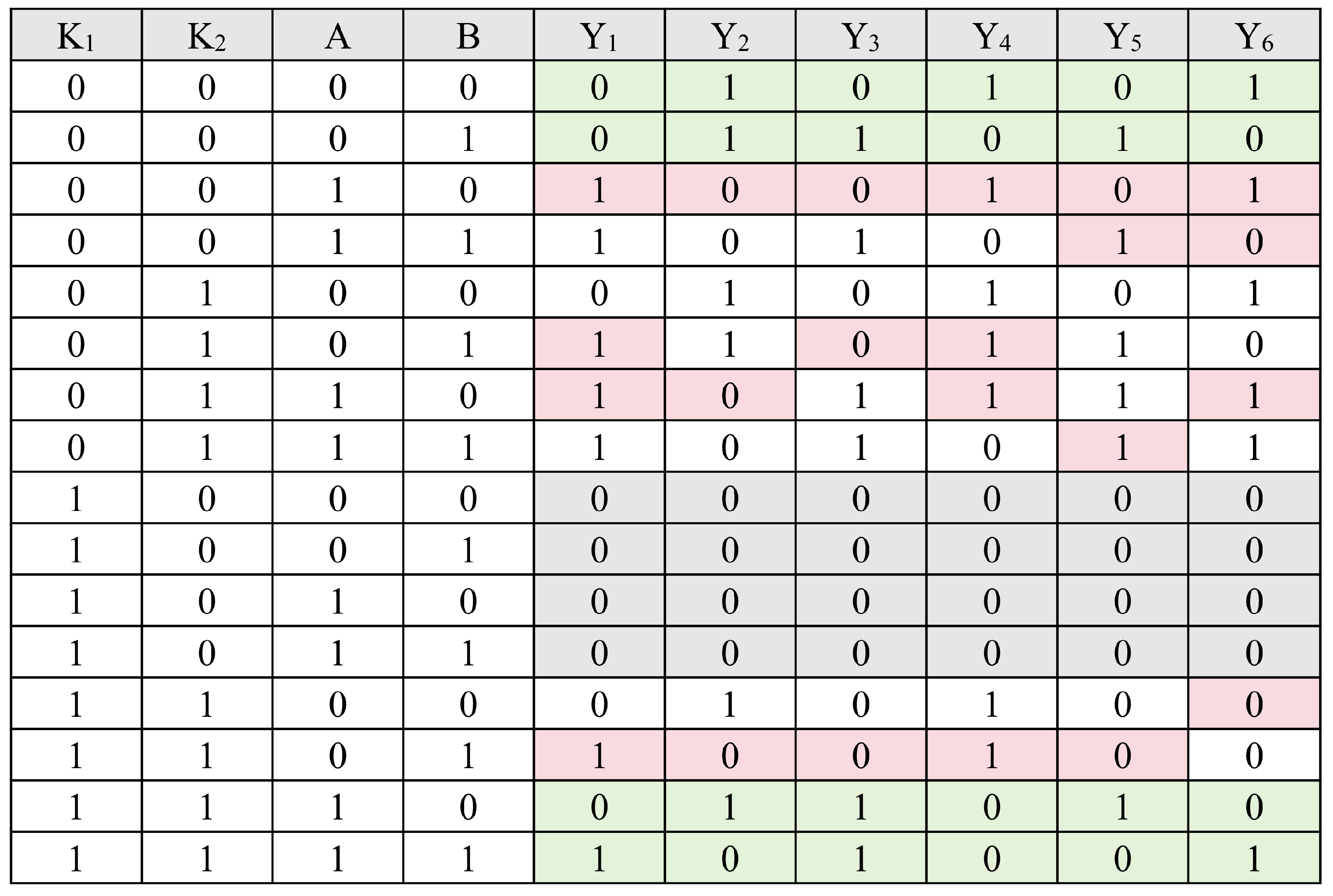
Table 1.
Logic expressions of RKC-m2 for six regular logic gates.
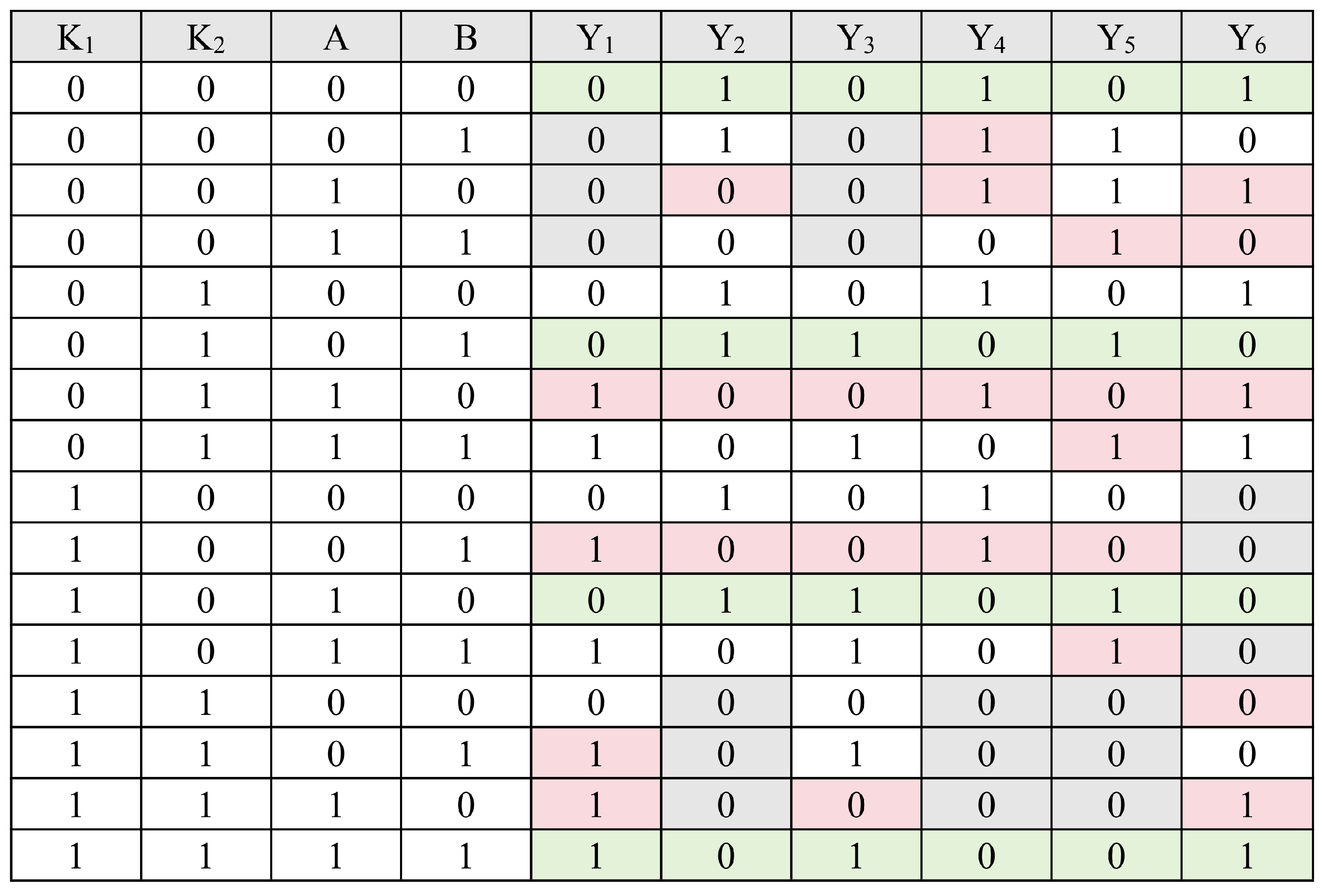
Similar to the construction process of the RKC instance at , RKC-m4 obtains the expression of the final key-controlled circuit corresponding to this original design gate, i.e., , by strategically flipping x to 1 and appropriately increasing the minterms, which is implemented as shown in Figure 2c. Based on the construction process of the RKC-m4 instance, we have respectively designed the key-controlled circuits for six logic gates, including AND, NAND, OR, NOR, XOR, and XNOR, at . The specific implementation of these key-controlled circuits is shown in Figure 5, where , , , , , and denote the outputs of the key-controlled circuits corresponding to AND, NAND, OR, NOR, XOR, and XNOR, respectively. Table 2 summarizes the logic expressions of the above six key-controlled circuits at . Figure 6 shows the truth table of each key-controlled circuit at .
As can be seen from Table 2, the logic expressions of the proposed RKC-m4 consist of only 2 AND-subequations, each of which contains no more than 3 variables, and for most of the RKC-m4 of the regular logic gates, the number of variables contained in each AND-subequation is 2. From the perspective of hardware implementation, the proposed RKC-m4 will not result in significant hardware overhead. Likewise, as can be seen from Figure 6, for each key combination, there is at least one circuit input pattern that produces an erroneous output. Hence, there exists no single key combination in the proposed RKC-m4 that is capable of unlocking all possible combinations of the circuit inputs, thereby being resistant to the SAT attack.
Table 2.
Logic expressions of RKC-m4 for six regular logic gates.
In addition, The LUT-based tamper-proof memory in RKC is designed as a configurable key storage unit, wherein the correct key is permanently embedded during the manufacturing phase, remains inaccessible or unmodifiable from outside the chip, thereby ensuring the security of key storage. The structure of this memory bears some resemblance to the wire entanglement technique proposed in Anti-SAT [14], with its core innovation being the reconfiguration of the MUX—originally used for signal obfuscation—into a fundamental component of the tamper-proof memory. The correct key is loaded into the data input of the MUX and transmitted to a locked circuit via its output, while the MUX’s select line is driven by the circuit input signal, as shown in Figure 2b,c. The value of design parameter m can affect the specific implementation of the LUT-based tamper-proof memory: when , the outputs of both , depend on the circuit input A; when , the outputs of , depend on the circuit inputs A, B, respectively.
It is worth noting that hardware overhead can be reduced through ingenious design of the storage structure. Specifically, observing the mapping relationship between the stored key and the unlocking key arriving at the locked circuit as in Figure 2b,c reveals: if the cells originally used to store “1” in and are replaced by cells storing “0” with the output fed through an inverter to the second input of the MUX, the actual storage of “1” values becomes unnecessary. Since the area of the inverter is significantly smaller than that of a complete storage cell, this strategy can reduce the storage space required for each key by nearly 50%, thereby lowering the overall storage demand to a level comparable to that of traditional tamper-proof memory. Therefore, from the perspective of hardware complexity, the primary hardware overhead of the LUT-based tamper-proof memory in this paper stems from the memory cells and MXUes. By adopting the simplest 2:1 MUX structure, the single-unit area overhead is approximately 3 to 5 standard logic gates. Hence, even when the number of locked bits increases to hundreds, the overall hardware overhead occupies a negligible area within the integrated circuit, posing no significant burden on the design. Note that the above LUT-based tamper-proof memory and its improved version will be likewise applicable to the multi-input key-controlled circuits (MKCs) presented in Section 4.2.
Figure 5.
RKC-m4 of six regular logic gates: (a) AND. (b) NAND. (c) OR. (d) NOR. (e) NOR. (f) XNOR.
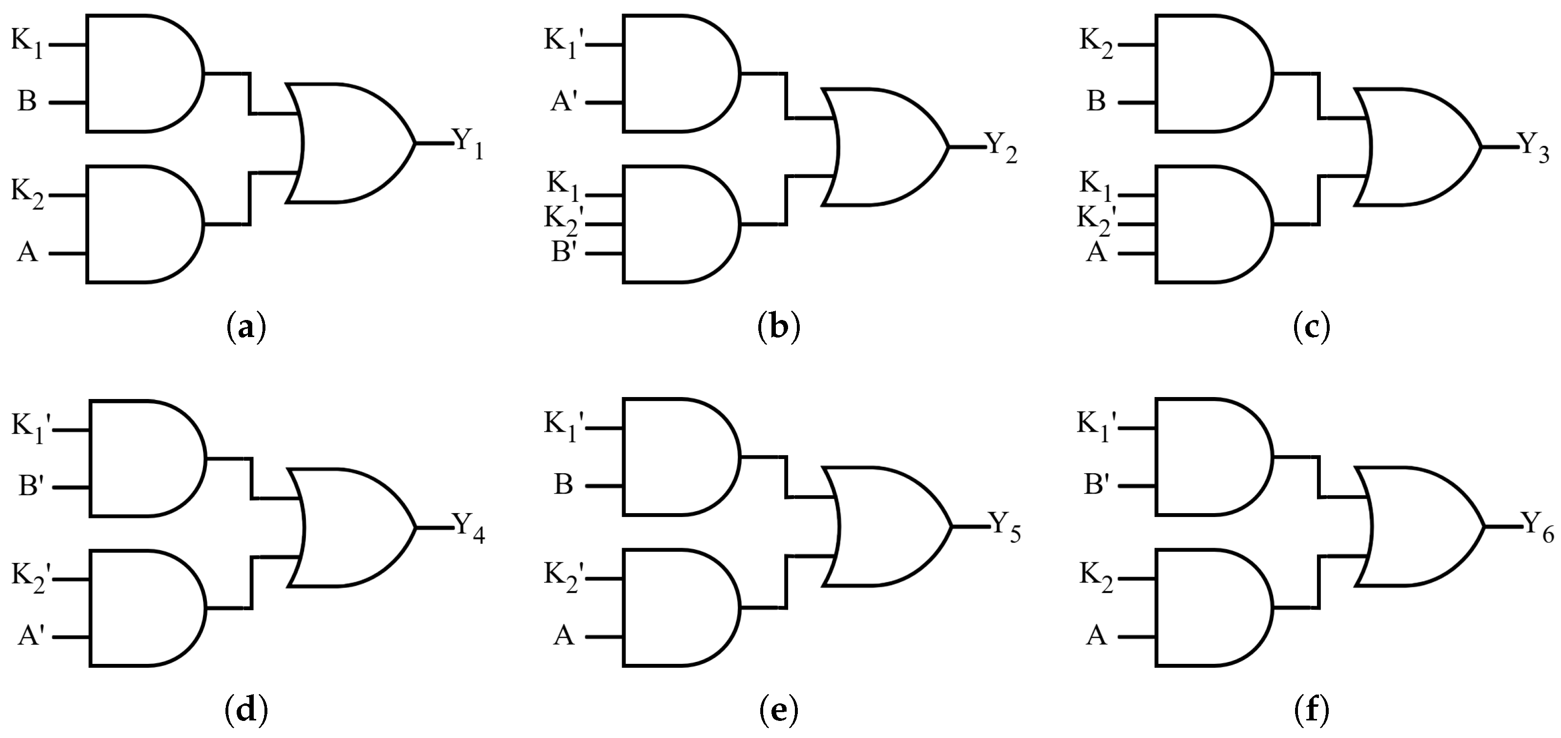
Figure 6.
Truth table of RKC-m4 for six regular logic gates. Note: The green-filled portion indicates the correct outputs for the corresponding circuit input patterns under the correct key combinations; the red-filled portion indicates the incorrect outputs for some circuit input patterns under a certain key combination; and the gray-filled portion indicates the same output 0 of all the circuit input patterns under a specific key combination. when there is an overlap between the gray-filled portion and the green/red-filled portion, the green/red-filled portion is used in priority for illustration.
Nevertheless, the security of this memory remains vulnerable to potential threats. First, without appropriate protections, attackers may infer key information through side-channel analysis (e.g., timing [37], power consumption [38], electromagnetic leakage [39,40]). Second, during prolonged utilization, the FPGA or ASIC may be subjected to physical attacks (e.g., microprobing [41], laser ablation [42]), leading to key leakage. Therefore, in practical deployments, the system circuit’s security can be further enhanced by integrating Physical Unclonable Functions (PUFs) [43] or encrypted access mechanisms.
4.2. Multi-Input Key-Controlled Circuits (MKC)
The regular logic gates, such as AND, NAND, OR, NOR, XOR, XNOR, etc., in integrated circuits (ICs) do not exist independently of a circuit design; rather, the inputs and outputs of the different gates establish interconnections to form a circuit with specific functions. In order to achieve stronger functional obfuscation and structural obfuscation as well as to validate the extensibility of the proposed method in the modified logic locking design framework, we propose a new multi-input key-controlled circuit by logically locking circuit topologies with multiple inputs based on the line connections established between different logic gates, which is named as MKC. Similar to RKC, the specific implementation of MKC is determined by the setting of the number m of circuit input sets in addition to the type of circuit topologies. We will expand MKC horizontally by modifying the value of the design parameter m, obtaining two logic-locking design circuits for and .
Unlike the RKC, the pending-locking design of MKC is extended from a logic gate with dual inputs to a circuit topology with multiple inputs. Consider an example of the MKC shown in Figure 7. Figure 7a–f show respectively the original design topology and its truth table, the MKC and its K-Map for replacing this original design topology at , and the MKC and its K-Map for replacing this original design topology at . A locked design can be obtained by replacing the original design topology shown in Figure 7a with the MKC shown in Figure 7b,c.
Figure 7.
Example of the multi-input key-controlled circuits. (a) Original design topology. (b) Multi-input key-controlled circuit after replacement at . (c) Multi-input key-controlled circuit after replacement at . (d) Truth table for the original design topology. (e) K-Map of the multi-input key-controlled circuit after replacement at . (f) K-Map of the multi-input key-controlled circuit after replacement at . Note: The input patterns enclosed by the red, green, and blue dashed boxes represent subequations of the key-controlled circuits, respectively. The expressions in both illustrated examples consist of three subequations.
(1) At . We represent the multi-input key-controlled circuits constructed at as MKC-m2. MKC-m2 divides the circuit input pattern into 2 sets, i.e., , , and then selects 2 combinations from the possible key combinations, i.e., , for unlocking the circuit output of the two circuit input sets, and , respectively. Based on the truth table of the AND-NAND circuit topology in Figure 7d, the output logic relationship of the MKC-m2 for constructing this topology is illustrated in the K-Map shown in Figure 7e. The logic output under the corresponding unlocking circuit input sets , of , , corresponds one-to-one with the logic output of the AND-NAND circuit topology in Figure 7d under each input pattern, and for the rest of the input patterns (which contain the key inputs and the circuit inputs), the logic output is denoted by using the “don’t care” term x.
If the “don’t care” terms (x) are default set to 0, the constructed MKC will behave as a more massive AND-OR equation (its AND-subequations contain many variables), i.e., , resulting in significantly increased hardware overhead. On the other hand, if the “don’t care” terms are default set to 1, there exists a single key combination that can unlock all possible combinations of the circuit inputs, which would render the locking design meaningless. To solve the problems caused by the above two extreme cases, we need to strategically flip x to 1. We obtain the expression of the constructed final MKC, i.e., , based on the distribution of 1 in Figure 7e, by merging the minterms according to the simplification rule of K-Map as shown by the red, green, and blue dashed framed parts in this figure, where different colored dashed framed parts indicate different AND-subequations. Unlike the construction process of the RKC instance, the MKC-m2 of this AND-NAND circuit topology does not deliberately retain the completely irrelevant minterms since the circuit topology with multiple inputs expands the input space, but instead constructs the smaller MKC that depends on all inputs (i.e., , , A, B, C) based on the distribution of 1 in Figure 7e, which is implemented as shown in Figure 7b.
Based on the construction process of the above MKC instance, we have respectively designed the MKC for six circuit topologies, including AND-AND, AND-NAND, AND-OR, AND-NOR, AND-XOR, and AND-, at . The specific implementation of these key-controlled circuits is shown in Figure 8, where , , , , , and denote the outputs of the MKC corresponding to AND-AND, AND-NAND, AND-OR, AND-NOR, AND-XOR, and AND-XNOR, respectively. Table 3 summarizes the logic expressions of the above six multi-input key-controlled circuits at . Figure 9 shows the truth table of each multi-input key-controlled circuit at . As can be seen from Figure 9, for each key combination, there is at least one circuit input pattern that produces an erroneous output. Hence, there exists no single key combination in the proposed MKC-m2 that is capable of unlocking all possible combinations of the circuit input, thereby being resistant to the SAT attack.
Figure 8.
MKC-m2 of six circuit topologies: (a) AND-AND. (b) AND-NAND. (c) AND-OR. (d) AND-NOR. (e) AND-NOR. (f) AND-XNOR.
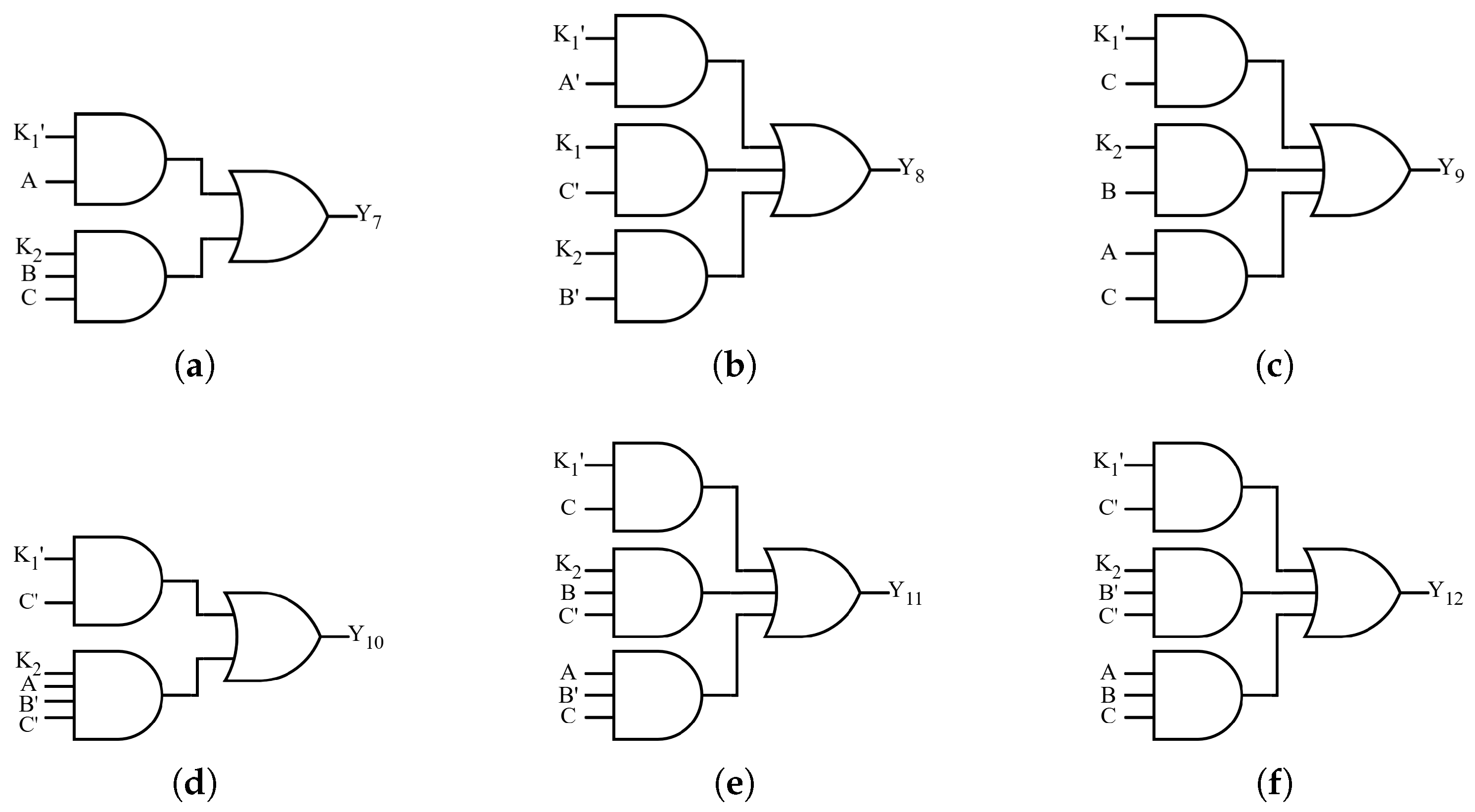
Figure 9.
Truth table of MKC-m2 for six circuit topologies. Note: The green-filled portion indicates the correct outputs for the corresponding circuit input patterns under the correct key combinations; the red-filled portion indicates the incorrect outputs for some circuit input patterns under a certain key combination; and the gray-filled portion indicates the same output 0 of all the circuit input patterns under a specific key combination. when there is an overlap between the gray-filled portion and the green/red-filled portion, the green/red-filled portion is used in priority for illustration.
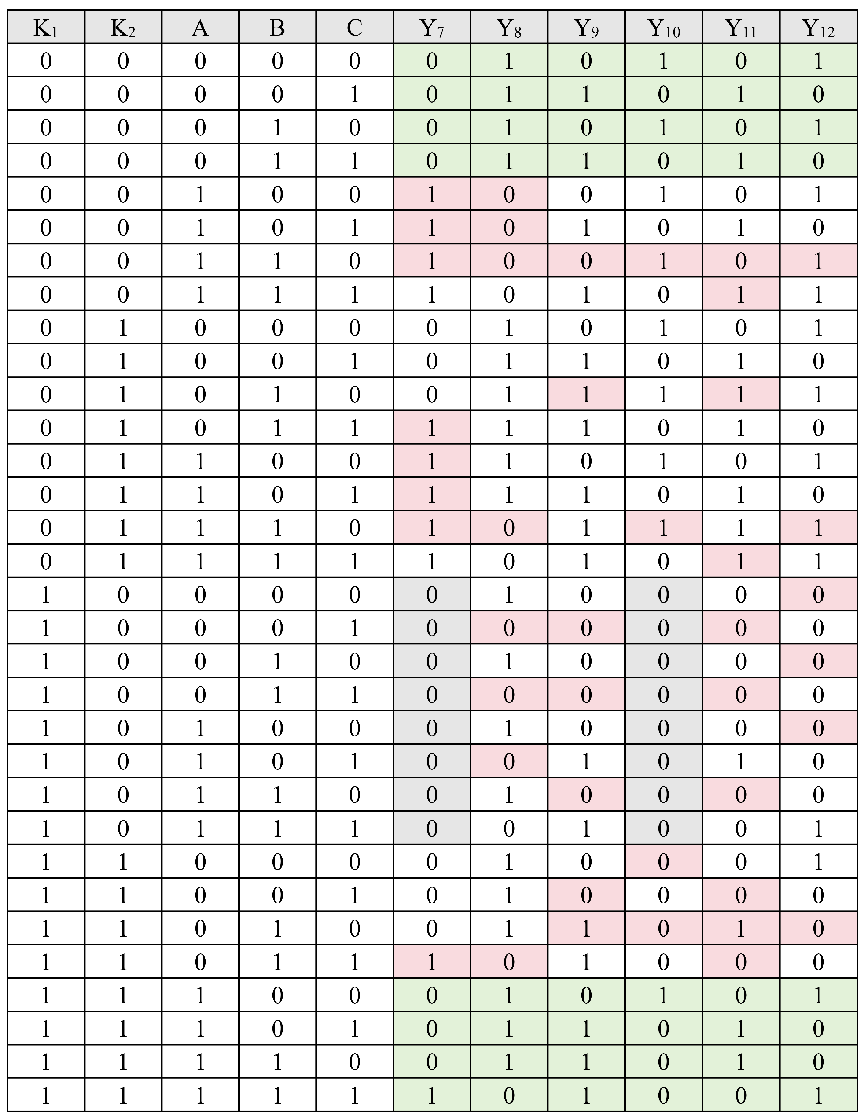
Table 3.
Logic expressions of MKC-m2 for six circuit topologies.
(2) At . We represent the multi-input key-controlled circuits constructed at as MKC-m4. MKC-m4 divides the circuit input pattern into 4 sets, i.e., , , , , and then selects 4 combinations from the possible key combinations, i.e., , for unlocking the circuit output of the four circuit input sets, , , and , respectively. Based on the truth table of the AND-NAND circuit topology in Figure 7d, the output logic relationship of the MKC-m4 for constructing this topology is illustrated in the K-Map shown in Figure 7f. The logic output under the corresponding unlocking circuit input sets , , , of , , , corresponds one-to-one with the logic output of the AND-NAND circuit topology in Figure 7d under each input pattern, and for the rest of the input patterns (which contain the key inputs and the circuit inputs), the logic output is denoted by using the “don’t care” term x.
Similar to the construction process of the MKC instance at , MKC-m4 obtains the expression of the final MKC corresponding to this original design topology, i.e., , by strategically flipping x to 1 and not intentionally retaining the completely irrelevant minterms, which is implemented as shown in Figure 7c. Based on the construction process of the above MKC instance, we have respectively designed the MKC for six circuit topologies, including AND-AND, AND-NAND, AND-OR, AND-NOR, AND-XOR, and AND-XNOR, at . The specific implementation of these key-controlled circuits is shown in Figure 10, where , , , , , and denote the outputs of the corresponding to AND-AND, AND-NAND, AND-OR, AND-NOR, AND-XOR, and AND-XNOR, respectively. Table 4 summarizes the logic expressions of the above six multi-input key-controlled circuits at . Figure 11 shows the truth table of each multi-input key-controlled circuit at .
Figure 10.
MKC-m4 of six circuit topologies: (a) AND-AND. (b) AND-NAND. (c) AND-OR. (d) AND-NOR. (e) AND-NOR. (f) AND-XNOR.
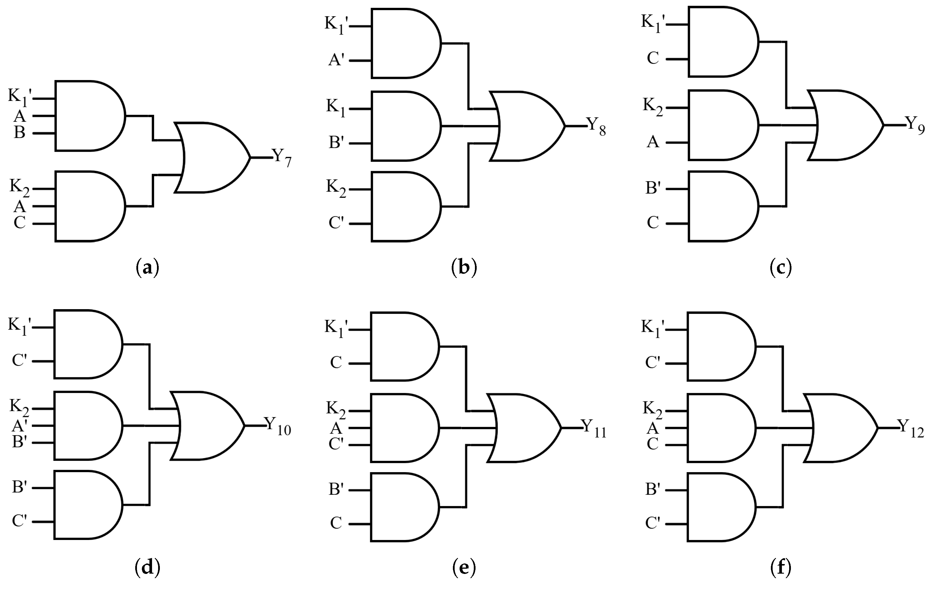
Figure 11.
Truth table of MKC-m4 for six circuit topologies. Note: The green-filled portion indicates the correct outputs for the corresponding circuit input patterns under the correct key combinations; the red-filled portion indicates the incorrect outputs for some circuit input patterns under a certain key combination; and the gray-filled portion indicates the same output 0 of all the circuit input patterns under a specific key combination. when there is an overlap between the gray-filled portion and the green/red-filled portion, the green/red-filled portion is used in priority for illustration.
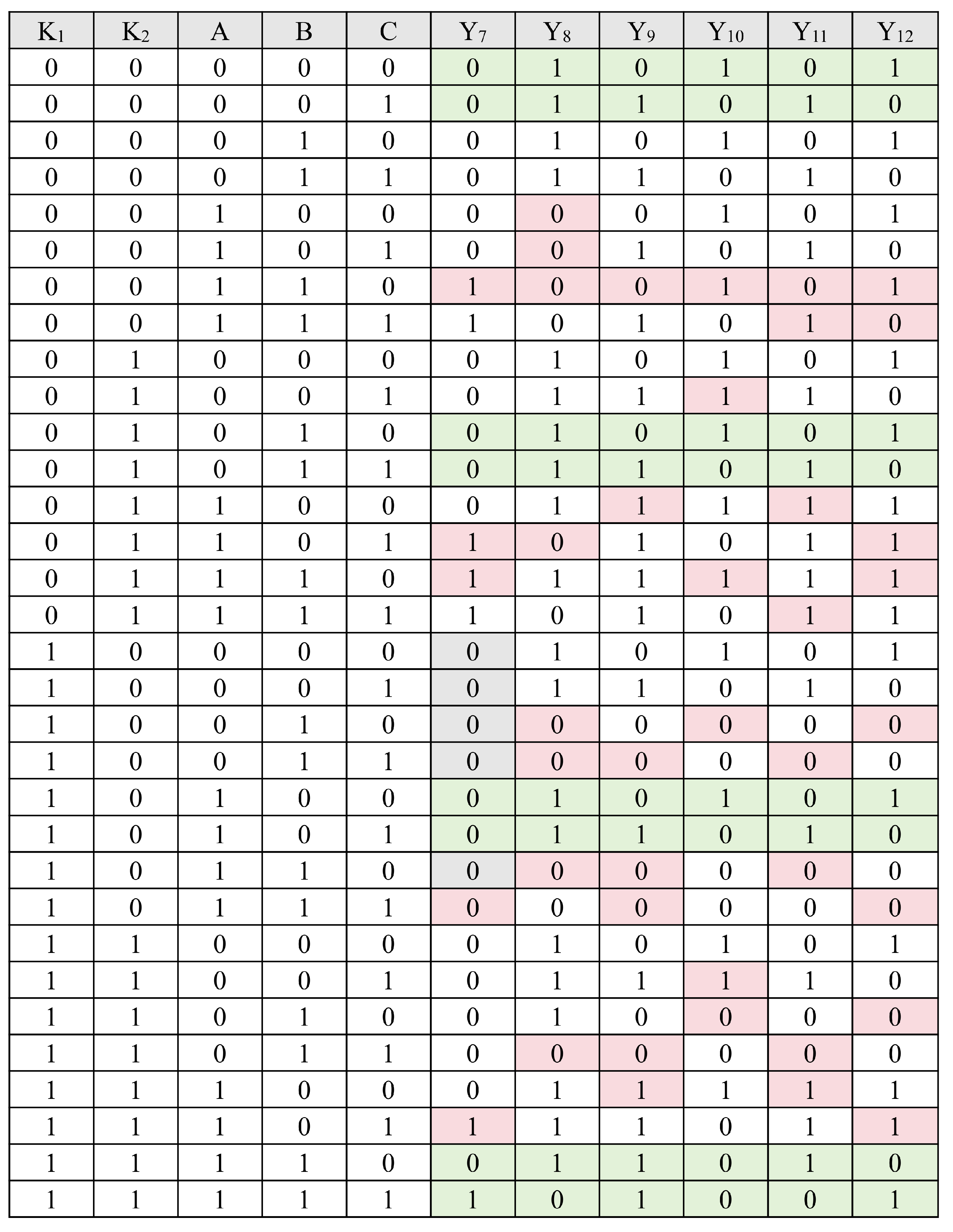
Table 4.
Logic expressions of MKC-m4 for six circuit topologies.
As can be seen from Table 4, most of the logic expressions of the proposed MKC-m4 consist of 3 AND-subequations, and there are a large number of AND-subequations only containing 2 variables. From Figure 11, it can be seen that the proposed MKC-m4 does not intentionally retain the completely irrelevant minterms; five out of the six circuit topologies’ MKC-m4 do not contain completely irrelevant minterms. The proposed MKC-m2 has similar characteristics to those described above. For each key combination, there is at least one circuit input pattern that produces an erroneous output. Hence, there exists no single key combination in the proposed MKC-m4 that is capable of unlocking all possible combinations of the circuit inputs, thereby being resistant to the SAT attack.
To date, we have obtained four logic-locking circuits, i.e., RKC-m2, RKC-m4, MKC-m2, and MKC-m4. Since the pending locking design of MKC is circuit topologies with multiple inputs, which expand the input space, the proposed MKC does not intentionally retain completely irrelevant minterms during the construction process, as in the proposed RKC, but builds smaller multi-input key-controlled circuits dependent on all inputs step by step based on the K-Map consisting of the “don’t care” term (x) and the deterministic logic (0, 1). The complexity of the proposed MKC is also higher than that of the proposed RKC due to the fact that the circuit topology consisting of two gates is more complicated than a single logic gate. The complexity of the proposed method (containing RKC, MKC) will be further verified and illustrated in Section 5.3. In addition, the independence of the intermediate network of the AND-NAND circuit topology shown in Figure 7a or other circuit topologies will affect the specific implementation of the proposed MKC during the locking process. If this intermediate network is independent, i.e., not connected to other networks, the entire circuit topology to be locked can be replaced with the proposed MKC; conversely, the proposed MKC can only replace a single logic gate. Figure 12 illustrates an instance of MKC-m2 performing logic locking. Due to the non-independence of in the target circuit topology to be locked, MKC can only replace a single AND gate G3 in the original circuit. If were connected merely to the input of G3 without any other network connections, MKC would be able to replace the entire target circuit topology in the original circuit.
Figure 12.
Example of MKC-m2 based logic locking. (a) Original circuit. (b) Locked circuit. The two red dashed boxes denote: (1) the original target circuit topology to be locked (left), and (2) the multi-input key-controlled circuit that replaces it (right).
Additionally, to avoid introducing additional timing overhead, the proposed RKC and MKC can be strategically applied to non-critical paths within the original circuit. The parameter , used to regulate timing perturbation, is set to a minimal value (e.g., equivalent to one standard cell delay) and affects only short paths. Therefore, the critical path delay of a circuit remains unchanged, thereby effectively preserving its timing performance without compromising functional correctness.
4.3. Security Analysis of the Proposed Method
Under the modified logic locking design framework, the proposed method prevents not only the SAT attack and its variants (AppSAT [5], Double-DIP [6]), the brute-force attack [11,12,44], but also other attacks such as the sensitization attack [10], the removal attack [17,18], the bypass attack [19], and so on.
Compared to the SAT attack, the AppSAT and Double-DIP attacks terminate early to return an approximation of the key, thus obtaining an approximation of the unlocked netlist. The main difference between these two attacks lies in the distinct conditions for early termination, which are explained in Section 1. There exists no single key combination in the proposed method that can unlock all possible combinations of the circuit inputs, thereby being resistant to the SAT attack. This defense mechanism applies equally to the AppSAT and Double-DIP attacks, where the strategic application of the proposed method can lead to high output corruption, rendering the approximate key obtained by the SAT attack variants meaningless for unlocking. At this point, the attacker has to rely on the brute-force attack to identify valid key combinations. Assuming that there are n-bit primary inputs and k-bit key inputs in the locked circuit, the quantitative security analysis of the proposed method against the brute-force attack is as follows. The proposed method selects m combinations from the possible key combinations for unlocking different circuit input sets, respectively. Since the circuit inputs are determined by the primary inputs, for an attacker, the valid key will be represented as the knowledge associated with m specific key combinations and their mappings to the primary input sets. The attacker needs to perform the following steps to obtain the valid key combinations: (1) determine the corresponding output of each key combination; (2) then select some or all of the combinations (whose number is greater than 1) from the possible key combinations to be permutated. The number of attempts required for step (1) is the maximum brute-force attack attempts required by conventional logic locking techniques, as shown in Equation (1).
The required attempts for step (2) are the number of all possible permutations of that key combination, as shown in Equation (2). Note that the reason for not starting from 1 is that the permutations obtained when correspond to the possible key combinations obtained in step (1).
In the worst case, the attacker needs to check all the permutations after determining the corresponding output of each key combination. Therefore, the maximum number of the brute-force attack required by the proposed method is the sum of and , as shown in Equation (3).
Compared to traditional logic locking techniques, the proposed method significantly increases the number of the brute-force attack required, where the increased number of the brute-force attack is . Thus, the proposed method significantly improves the security against the brute-force attack.
When the propagation path of a key bit to the output remains independent and is not interfered with by other key bits, the sensitization attack applies a particular input pattern to propagate that key bit to the output, which in turn parses the correct key bit. The logic locking circuit in the proposed method has two key inputs that interfere with each other, and the design makes it impossible for the sensitization attack to find a single key bit without interference from the other key bits, which in turn prevents the key value from being sensitized and propagated to the output. The removal attack identifies and removes inserted circuit modules that are resistant to the SAT attack from the locked design by structural or functional analysis. Since the proposed method replaces the original design gates/circuit topologies with the locking circuits to achieve logic locking without following any specific structure and function, the attacker has no way of knowing the replacement circuits and replaced gates/circuits, and consequently, there is no way to remove the replacement circuits from the locked design. The bypass attack utilizes the design features of the previously proposed SAT resilient logic locking techniques [13,14], such as inserted point function logic modules, low output corruption, etc., and constructs a linearly sized bypass circuit to restore the functionality of the locked circuit. The proposed method lacks the above design features, thereby reducing the effectiveness of the bypass attack.
4.4. Differentiation from GateLock
This paper proposes two locking schemes, RKC and MKC, by refining the logic locking design framework of GateLock. To avoid confusion, we summarize the differences between the proposed methods and GateLock as follows.
(1) The proposed method is introduced based on the modified logic locking design framework. We find that a series of published passive SAT resilient logic locking techniques have been developed based on the traditional logic locking design framework, and that the SAT attack and its variants exhibit formidable effectiveness against logic locking techniques under this design framework. As an active SAT resilient logic locking technique, the proposed method changes the traditional logic locking design framework and presents a new modified logic locking design framework. According to this design framework, researchers can develop new active SAT resilient logic locking techniques.
(2) To resolve the problems that there exists a single key combination that can unlock all possible combinations of the circuit inputs, and the constructed key-controlled circuits need to take significant hardware overhead, RKC strategically flips the “don’t care” term (x) to 1 by merging the minterms according to the simplification rule of K-Map. Moreover, RKC views , , A, and B as a whole and constructs key-controlled circuits that depend on all inputs by appropriately increasing the minterms. From the perspective of locking mechanism, the constraints of RKC are more relaxed and flexible compared with GateLock. From the perspective of concrete implementation, RKC requires less additional hardware overhead than GateLock.
(3) In order to achieve stronger functional and structural obfuscation as well as to verify the extensibility of the proposed method under the modified logic locking design framework, we present MKC by vertical expansion, whose pending locking design is expanded from logic gates with dual inputs to circuit topologies with multiple inputs. Since the circuit topology with multiple inputs expands the input space, MKC does not intentionally retain completely irrelevant minterms; instead, it constructs smaller multi-input key-controlled circuits that gradually depend on all inputs based on the distribution of the data in the K-Map. This is not reflected in GateLock.
(4) Similar to GateLock, rather than a conventional tamper-proof memory, the proposed method also utilizes a LUT-based tamper-proof memory, which according to the circuit inputs passes different key combinations to the locked circuit. However, compared to the conventional tamper-proof memory, GateLock requires m× storage space, and its extra mux is a multi-way vector mux controlled by two inputs. In contrast, the proposed method requires only 2× or even 1× storage space, with an extra mux that is the simplest 2:1 mux controlled by a single circuit input. In terms of theoretical analysis, the proposed method not only reduces the storage space but also decreases the complexity of the storage mechanism.
The above content outlines four distinctions between the proposed method and GateLock. In the next section, we will present the performance evaluation experiments and comparative analysis results to verify the superiority of the proposed method.
5. Experiments and Results
This section shows the performance evaluation experiments and comparative analysis results of the proposed method.
5.1. Experimental Setup
In this section, we provide the attack results, including the SAT attack and AppSAT attack, to evaluate the security performance of the proposed method, and analyze the hardware overhead of the proposed method and the other four comparative methods (i.e., GateLock, SKG-Lock, SKG-Lock+, CAS-Lock).
The experiments are executed on a 12th Gen Intel(R) Core(TM) i5-12500H processor running at 2.5 GHz with 16 GB RAM. The proposed method is implemented using the Verilog hardware description language. The key length (i.e., number of locked bits) is configurable within the range of 10 to 16 bits in increments of 2 (i.e., 10, 12, 14, and 16). The experiments for the SAT attack and AppSAT attack employed the open-source C++ implementation released by Kaveh Shamsi [1]. Since neither attack can recover the correct key under the proposed method, their solving processes terminate within an extremely short time due to unsatisfiable constraints. Therefore, no upper bound on solving time was set. The area and power consumption overhead of circuits are obtained using the Synopsys Design Compiler synthesis tool with TSMC 28 nm CMOS Process Standard Cell Library. All experiments are repeated 10 times, with results presented as average values. We utilize six benchmark circuits from the ISCAS’85 and MCNC benchmarks for logic locking, and the related statistics are shown in Table 5.
Table 5.
Statistics for the six benchmark circuits of the ISCAS’85 and MCNC benchmarks.
5.2. Attack Results
We employ four logic locking circuits—RKC-m2, RKC-m4, MKC-m2, and MKC-m4—included in the proposed method to perform gate-level or topology-level replacements on the target circuit. For the sake of uniform analysis, the locked bits are defined as the number of added key input bits. During the locking process, we randomly select gates/circuit topologies for locking in each benchmark circuit. To minimize bias in the hardware overhead analysis, both RKC and MKC are applied to the same gates or circuit topologies under identical locked bits.
We recorded the number of iterations and iteration time (s) required by the SAT attack for each locked circuit as the number of locked bits increased from 10 to 16 in steps of 2, and computed the average number of iterations and average iteration time at which the SAT attack terminated under the same locked bits, as shown in Figure 13a,b. It can be seen from the figure that the SAT attack terminates after several iterations, with an iteration time of only several seconds. Moreover, as expected, under the modified logic locking design framework, the SAT attack results of the proposed method are: (1) either eliminating all the keys, making the SAT attack impossible to model; (2) or returning an incorrect key that does not provide the correct output for all circuit input combinations. Therefore, we assert that the proposed method is secure against the SAT attack.
We also applied the proposed method to lock the c1355 benchmark circuit with 16 bits and launched the AppSAT attack against it. We used the same attack configuration as in [5]: applying 50 random queries after every 12 SAT iterations, with a settlement-threshold of 5. Since the AppSAT attack essentially remains a SAT-based attack, its objective is to return an approximate key satisfying the constraints. The proposed method is based on the modified logic-locking design framework, in which the correct key varies with the circuit inputs. For each key combination, at least one circuit input pattern produces an incorrect output, which is the case when locking using a single RKC/MKC. When the key size is expanded to larger scales such as 64 or 128 bits, RKC exhibits erroneous outputs for at least of the circuit input patterns, and RKC exhibits erroneous outputs for at least of the circuit input patterns, thereby achieving high output corruption. Consequently, the AppSAT attack also fails to obtain the correct key, as evidenced by the AppSAT attack results presented in Table 6.
Figure 13.
SAT attack results. (a) Average iterations for each locking circuit under different locked bits. (b) Average iteration time (s) for each locking circuit under different locked bits. Note: The SAT attack results in one of the following two scenarios: (1) either all keys are eliminated, making the SAT attack impossible to model, (2) or an incorrect key is returned that does not provide the correct output for all circuit input combinations.
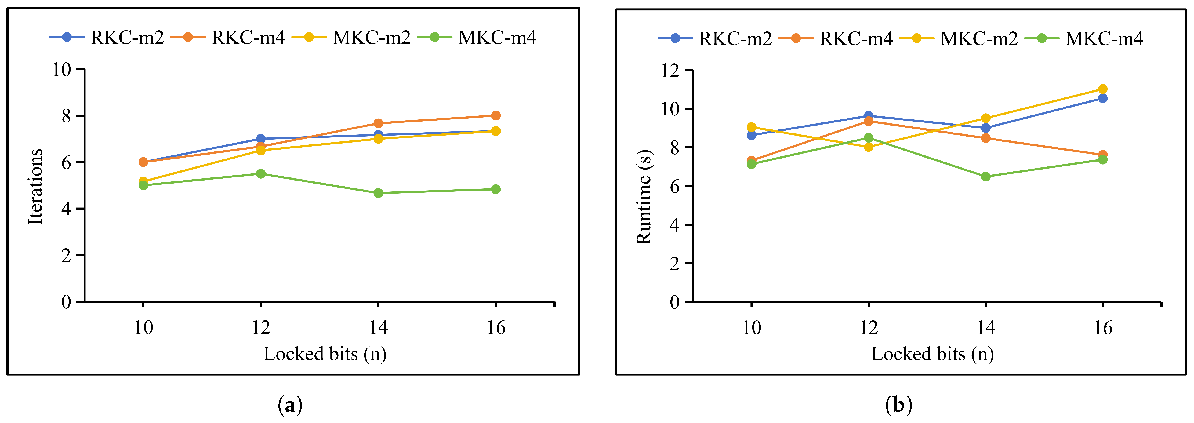
Table 6.
AppSAT Attack Results.
In summary, based on the results of the SAT attack and AppSAT attack, we can assert the security of the proposed method against the SAT attack [2] and its variants [5,6].
5.3. Hardware Overhead Analysis
We analyzed the hardware overhead generated by the four locking schemes RKC-m2, RKC-m4, MKC-m2, and MKC-m4 included in the proposed method, and compared them with the hardware overhead of four recently published locking schemes, i.e., GateLock [36], SKG-Lock [34], SKG-Lock+ [35], and CAS-Lock [20]. Considering the specificity of the locking mechanisms of the latter three comparison schemes, where the key inputs of SKG-Lock and SKG-Lock+ consist of the decoy key and the activation key, and CAS-Lock is formed by the construction of two complementary cascade trees, we adopt their generic settings, where the number of the decoy key bits of SKG-Lock and SKG-Lock+ is equal to the number of the activation key bits, and the number of locked bits in the specific implementation of these three schemes is the number of circuit input bits.
Figure 14 presents the hardware overhead analysis results for each locking scheme, from which we can obtain the following three pieces of information:
(1) Like GateLock, SKG-Lock, SKG-Lock+, and CAS-Lock, the hardware overhead of the proposed method tends to grow linearly with the increase of the locked bits, and its linear growth amplitude is extremely small. Specifically, under the same locking scheme, the area overhead between any two adjacent configurations (differing by 2 locked bits) ranges from 0.063 µm2 to 2.079 µm2, while the power overhead ranges from −0.0002 to 0.001 .
Figure 14.
Hardware overhead analysis results of each locking scheme (%). (a) Average area growth overhead of each locking scheme at different locked bits. (b) Average power growth overhead of each locking scheme at different locked bits.
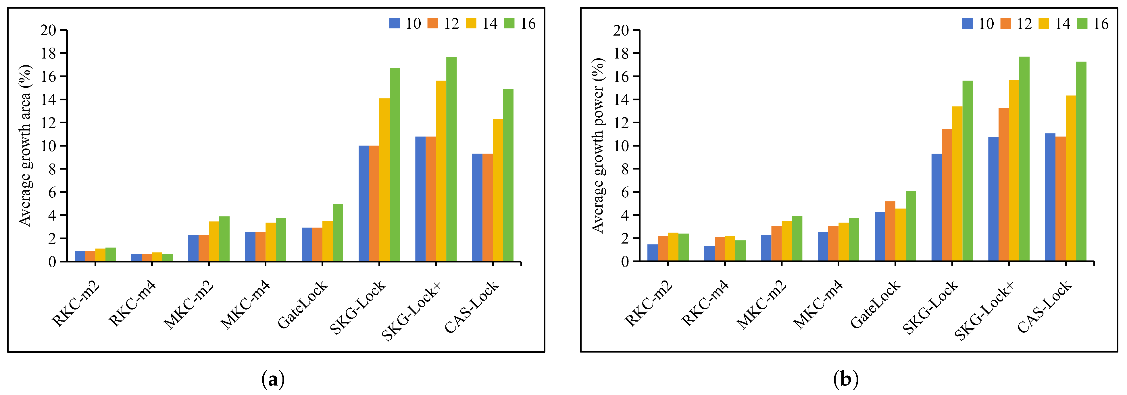
(2) Due to the higher complexity of MKC compared to RKC and the non-independence of in MKC—which results in only a single logic gate being replaced—the additional area overhead generated by MKC is slightly higher than that of RKC for the same locked bits. To minimize this hardware overhead, designers can select circuit topologies featuring independent for locking.
(3) In most cases, the hardware overhead comparison relationship of each locking scheme is: RKC < MKC < GateLock < CAS-Lock < SKG-Lock < SKG-Lock+. When the number of locked bits is 16, the average area growth percentages for SKG-Lock, SKG-Lock+, and CAS-Lock are 16.68%, 17.66%, and 14.87%, respectively, while their average power growth percentages are 15.63%, 17.7%, and 17.27%, respectively—significantly higher than those of the other three schemes (i.e., RKC, MKC, and GateLock). Compared to GateLock, although MKC exhibits relatively higher complexity, its hardware growth percentage remains consistently lower than that of GateLock.
Table 7 shows the bit average growth hardware overhead data for each locking scheme, which is obtained by subtracting the 16-bit locking overhead from the 10-bit locking overhead and dividing by the locked bits difference 6. As can be seen from the table, the bit average growth area overhead of GateLock is 3.45/4.57 times and 1.13/1.91 times that of RKC-m2/RKC-m4, MKC-m2/MKC-m4, respectively; the bit average growth area overhead of SKG-Lock is 11.46/15.20 times and 3.76/6.37 times that of RKC-m2/RKC-m4, MKC-m2/MKC-m4, respectively; the bit average growth area overhead of SKG-Lock+ is 11.95/15.8 times and 3.92/6.64 times that of RKC-m2/RKC-m4, MKC-m2/MKC-m4, respectively; and the bit average growth area overhead of CAS-Lock is 9.68/12.84 times and 3.18/5.38 times that of RKC-m2/RKC-m4, MKC-m2/MKC-m4, respectively. This significant multiplicative relationship illustrates the unique advantage of the proposed method in terms of hardware overhead.
Table 7.
Bit average growth hardware overhead data for each locking scheme.
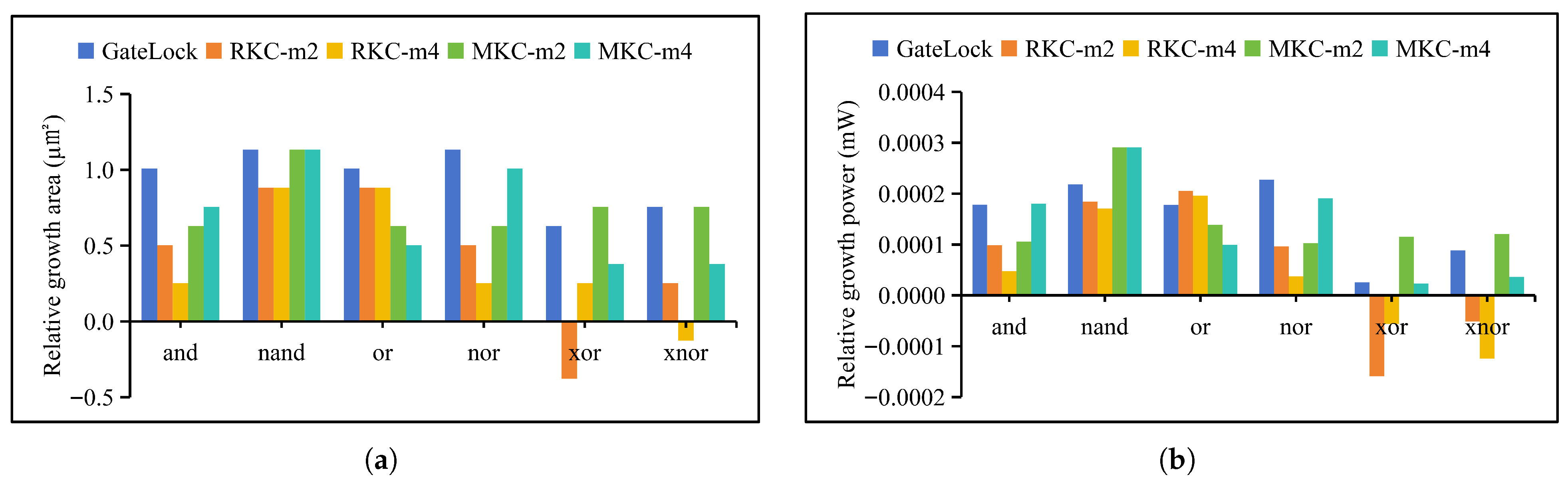
In addition, we analyze the relative hardware overhead of the individual locking topologies for each locking scheme, defined as the difference between the overhead of the locking circuit topology and that of the pending locking component, as shown in Figure 15. Since the locking component of MKC is implemented in the form of AND-X, for ease of representation, it is abbreviated uniformly as X, using the same notation as the other two locking schemes (i.e., GateLock and RKC), where X denotes the logic gate type. From the figure, it can be seen that, in most cases, the relative hardware growth overhead of the individual locking topologies in the proposed method is lower than that of GateLock, and RKC even exhibits negative relative hardware growth overhead values. Analyzed from a global perspective, the relative area growth overhead of the proposed method is in the range of −0.378 µm2 to 1.134 µm2, and the relative power growth overhead is in the range of −0.0002 to 0.0003 , which results in very low additional hardware overhead for the logic locking technique with a step size of 2. From this, we can infer that the additional hardware overhead generated by the locking topologies of other pending locking components (X-X) not covered in this paper is unlikely to deviate significantly from the ranges reported above. Thus, this relative hardware overhead analysis results prove the extensibility of the proposed method on hardware implementation.
In summary, based on the hardware overhead analysis results, the average bit growth hardware overhead data for each locking scheme and the relative hardware overhead analysis results for its individual locking topologies, we can assert the superiority of the proposed method in terms of hardware overhead.
Figure 15.
Relative hardware overhead analysis results for the individual locking topologies of each locking scheme. (a) Relative area growth overhead of different locking topologies for each locking scheme, Unit: µm2. (b) Relative power growth overhead of different locking topologies for each locking scheme, Unit: .
6. Conclusions
This paper presents a novel replacement-based key-controlled circuit (RKC). This structure effectively undermines the feasibility foundation of the existing SAT attack and its derivative methods by reconstructing the design framework of traditional logic locking. To further enhance the security of the logic locking scheme in terms of functional and structural obfuscation, and to validate the scalability potential of the proposed framework, this paper introduces a vertical scaling strategy. It constructs a class of multi-input key-controlled circuit (MKC), which is also based on replacement applied to the locking design and is applicable to more complex locking scenarios. Moreover, we also perform horizontal expansion on the two proposed circuits by modifying the value of the design parameter m, resulting in four logic locking design circuits, each of which includes six different sub-circuits.
Through the security analysis, we conclude that under the modified logic locking design framework, the proposed method can prevent not only the SAT attack and its variants (AppSAT, Double-DIP), the brute-force attack, but also other attacks, such as the sensitization attack, the removal attack, the bypass attack, and so on. The hardware overhead analysis results, the bit average growth hardware overhead data for each locking scheme, and the relative hardware overhead analysis results for its individual locking topologies obtained from the relevant experiments performed on the six benchmark circuits selected from the ISCAS’85 and MCNC benchmarks validate the superiority and scalability of the proposed method in multiple dimensions.
Author Contributions
Conceptualization, W.W. and L.Z.; methodology, W.W. and L.Z.; software, L.Z.; validation, W.W. and L.Z.; formal analysis, L.Z.; investigation, L.Z.; data curation, L.Z.; writing—original draft preparation, W.W. and L.Z.; writing—review and editing, W.W. and L.Z.; visualization, L.Z.; supervision, W.W. and S.C.; project administration, S.C. All authors have read and agreed to the published version of the manuscript.
Funding
This research was supported by the Natural Science Foundation of Hunan Province under Grant Nos. 2023JJ30316 and 2022JJ10052, the Scientific Research Fund of Hunan Provincial Education Department under Grant No. 23A0686, and the National Natural Science Foundation of China under Grant No. 62172058.
Institutional Review Board Statement
Not applicable.
Informed Consent Statement
Not applicable.
Data Availability Statement
The raw data supporting the conclusions of this article will be made available by the authors on request.
Conflicts of Interest
The authors declare no conflicts of interest.
Correction Statement
This article has been republished with a minor correction to the existing affiliation information. This change does not affect the scientific content of the article.
References
- Shamsi, K.; Meade, T.; Li, M.; Pan, D.Z.; Jin, Y. On the Approximation Resiliency of Logic Locking and IC Camouflaging Schemes. IEEE Trans. Inf. Forensics Secur. 2019, 14, 347–359. [Google Scholar] [CrossRef] [Scilit]
- Subramanyan, P.; Ray, S.; Malik, S. Evaluating the security of logic encryption algorithms. In Proceedings of the 2015 IEEE International Symposium on Hardware Oriented Security and Trust (HOST), Washington, DC, USA, 5–7 May 2015; pp. 137–143. [Google Scholar] [CrossRef] [Scilit]
- Yasin, M.; Sengupta, A.; Nabeel, M.T.; Ashraf, M.; Rajendran, J.J.; Sinanoglu, O. Provably-Secure Logic Locking: From Theory to Practice. In Proceedings of the 2017 ACM SIGSAC Conference on Computer and Communications Security (CCS ’17), New York, NY, USA, 30 October–3 November 2017; pp. 1601–1618. [Google Scholar] [CrossRef] [Scilit]
- Chakraborty, A.; Jayasankaran, N.G.; Liu, Y.; Rajendran, J.; Sinanoglu, O.; Srivastava, A.; Xie, Y.; Yasin, M.; Zuzak, M. Keynote: A Disquisition on Logic Locking. IEEE Trans. Comput.-Aided Des. Integr. Circuits Syst. 2020, 39, 1952–1972. [Google Scholar] [CrossRef] [Scilit]
- Shamsi, K.; Li, M.; Meade, T.; Zhao, Z.; Pan, D.Z.; Jin, Y. AppSAT: Approximately deobfuscating integrated circuits. In Proceedings of the 2017 IEEE International Symposium on Hardware Oriented Security and Trust (HOST), Mclean, VA, USA, 1–5 May 2017; pp. 95–100. [Google Scholar] [CrossRef] [Scilit]
- Shen, Y.; Zhou, H. Double DIP: Re-Evaluating Security of Logic Encryption Algorithms. In Proceedings of the Great Lakes Symposium on VLSI 2017 (GLSVLSI ’17), New York, NY, USA, 10–12 May 2017; pp. 179–184. [Google Scholar] [CrossRef] [Scilit]
- Roy, J.A.; Koushanfar, F.; Markov, I.L. EPIC: Ending Piracy of Integrated Circuits. In Proceedings of the 2008 Design, Automation and Test in Europe, Munich, Germany, 10–14 March 2008; pp. 1069–1074. [Google Scholar] [CrossRef] [Scilit]
- Roy, J.; Koushanfar, F.; Markov, I. Ending Piracy of Integrated Circuits. Computer 2010, 43, 30–38. [Google Scholar] [CrossRef] [Scilit]
- Baumgarten, A.; Tyagi, A.; Zambreno, J. Preventing IC Piracy Using Reconfigurable Logic Barriers. IEEE Des. Test Comput. 2010, 27, 66–75. [Google Scholar] [CrossRef] [Scilit]
- Rajendran, J.; Pino, Y.; Sinanoglu, O.; Karri, R. Security analysis of logic obfuscation. In Proceedings of the DAC Design Automation Conference 2012, San Francisco, CA, USA, 3–7 June 2012; pp. 83–89. [Google Scholar] [CrossRef] [Scilit]
- Yasin, M.; Rajendran, J.J.; Sinanoglu, O.; Karri, R. On Improving the Security of Logic Locking. IEEE Trans. Comput.-Aided Des. Integr. Circuits Syst. 2016, 35, 1411–1424. [Google Scholar] [CrossRef] [Scilit]
- Rajendran, J.; Zhang, H.; Zhang, C.; Rose, G.S.; Pino, Y.; Sinanoglu, O.; Karri, R. Fault Analysis-Based Logic Encryption. IEEE Trans. Comput. 2015, 64, 410–424. [Google Scholar] [CrossRef] [Scilit]
- Yasin, M.; Mazumdar, B.; Rajendran, J.J.V.; Sinanoglu, O. SARLock: SAT attack resistant logic locking. In Proceedings of the 2016 IEEE International Symposium on Hardware Oriented Security and Trust (HOST), McLean, VA, USA, 3–5 May 2016; pp. 236–241. [Google Scholar] [CrossRef] [Scilit]
- Xie, Y.; Srivastava, A. Anti-SAT: Mitigating SAT Attack on Logic Locking. IEEE Trans. Comput.-Aided Des. Integr. Circuits Syst. 2019, 38, 199–207. [Google Scholar] [CrossRef] [Scilit]
- Li, M.; Shamsi, K.; Meade, T.; Zhao, Z.; Yu, B.; Jin, Y.; Pan, D.Z. Provably secure camouflaging strategy for IC protection. In Proceedings of the 35th International Conference on Computer-Aided Design (ICCAD ’16), New York, NY, USA, 7–10 November 2016. [Google Scholar] [CrossRef] [Scilit]
- Liu, Y.; Zuzak, M.; Xie, Y.; Chakraborty, A.; Srivastava, A. Strong Anti-SAT: Secure and Effective Logic Locking. In Proceedings of the 2020 21st International Symposium on Quality Electronic Design (ISQED), Santa Clara, CA, USA, 25–26 March 2020; pp. 199–205. [Google Scholar] [CrossRef] [Scilit]
- Yasin, M.; Mazumdar, B.; Sinanoglu, O.; Rajendran, J. Security analysis of Anti-SAT. In Proceedings of the 2017 22nd Asia and South Pacific Design Automation Conference (ASP-DAC), Chiba, Japan, 16–19 January 2017; pp. 342–347. [Google Scholar] [CrossRef] [Scilit]
- Yasin, M.; Mazumdar, B.; Sinanoglu, O.; Rajendran, J. Removal Attacks on Logic Locking and Camouflaging Techniques. IEEE Trans. Emerg. Top. Comput. 2020, 8, 517–532. [Google Scholar] [CrossRef] [Scilit]
- Xu, X.; Shakya, B.; Tehranipoor, M.M.; Forte, D. Novel Bypass Attack and BDD-based Tradeoff Analysis Against All Known Logic Locking Attacks. In Proceedings of the Cryptographic Hardware and Embedded Systems—CHES 2017, Taipei, Taiwan, 25–28 September 2017; pp. 189–210. [Google Scholar]
- Shakya, B.; Xu, X.; Tehranipoor, M.; Forte, D. CAS-Lock: A Security-Corruptibility Trade-off Resilient Logic Locking Scheme. IACR Trans. Cryptogr. Hardw. Embed. Syst. 2019, 2020, 175–202. [Google Scholar] [CrossRef] [Scilit]
- Yasin, M.; Sengupta, A.; Schafer, B.; Makris, Y.; Sinanoglu, O.; Rajendran, J. What to lock? Functional and parametric locking. In Proceedings of the GLSVLSI 2017—Great Lakes Symposium on VLSI 2017, Banff, AB, Canada, 10–12 May 2017; Association for Computing Machinery: New York, NY, USA, 2017; pp. 351–356. [Google Scholar] [CrossRef] [Scilit]
- Sirone, D.; Subramanyan, P. Functional Analysis Attacks on Logic Locking. In Proceedings of the 2019 Design, Automation & Test in Europe Conference & Exhibition (DATE), Florence, Italy, 25–29 March 2019; pp. 936–939. [Google Scholar] [CrossRef] [Scilit]
- Zhou, H.; Shen, Y.; Rezaei, A. Vulnerability and Remedy of Stripped Function Logic Locking. Cryptology ePrint Archive, Paper 2019/139. 2019. Available online: https://eprint.iacr.org/2019/139.pdf (accessed on 13 January 2026).
- Yang, F.; Tang, M.; Sinanoglu, O. Stripped Functionality Logic Locking with Hamming Distance-Based Restore Unit (SFLL-hd)–Unlocked. IEEE Trans. Inf. Forensics Secur. 2019, 14, 2778–2786. [Google Scholar] [CrossRef] [Scilit]
- Sengupta, A.; Nabeel, M.; Yasin, M.; Sinanoglu, O. ATPG-based cost-effective, secure logic locking. In Proceedings of the 2018 IEEE 36th VLSI Test Symposium (VTS), San Francisco, CA, USA, 22–25 April 2018; pp. 1–6. [Google Scholar] [CrossRef] [Scilit]
- Sengupta, A.; Nabeel, M.; Limaye, N.; Ashraf, M.; Sinanoglu, O. Truly Stripping Functionality for Logic Locking: A Fault-Based Perspective. IEEE Trans. Comput.-Aided Des. Integr. Circuits Syst. 2020, 39, 4439–4452. [Google Scholar] [CrossRef] [Scilit]
- Shamsi, K.; Li, M.; Meade, T.; Zhao, Z.; Pan, D.Z.; Jin, Y. Cyclic Obfuscation for Creating SAT-Unresolvable Circuits. In Proceedings of the Great Lakes Symposium on VLSI 2017 (GLSVLSI ’17), New York, NY, USA, 10–12 May 2017; pp. 173–178. [Google Scholar] [CrossRef] [Scilit]
- Zhou, H.; Jiang, R.; Kong, S. CycSAT: SAT-based attack on cyclic logic encryptions. In Proceedings of the 2017 IEEE/ACM International Conference on Computer-Aided Design (ICCAD), Irvine, CA, USA, 13–16 November 2017; pp. 49–56. [Google Scholar] [CrossRef] [Scilit]
- Shen, Y.; Li, Y.; Rezaei, A.; Kong, S.; Dlott, D.; Zhou, H. BeSAT: Behavioral SAT-based attack on cyclic logic encryption. In Proceedings of the 24th Asia and South Pacific Design Automation Conference (ASPDAC ’19), New York, NY, USA, 21–24 January 2019; pp. 657–662. [Google Scholar] [CrossRef] [Scilit]
- Shamsi, K.; Li, M.; Pan, D.Z.; Jin, Y. Cross-Lock: Dense Layout-Level Interconnect Locking using Cross-bar Architectures. In Proceedings of the 2018 Great Lakes Symposium on VLSI (GLSVLSI ’18), New York, NY, USA, 23–25 May 2018; pp. 147–152. [Google Scholar] [CrossRef] [Scilit]
- Roshanisefat, S.; Mardani Kamali, H.; Sasan, A. SRCLock: SAT-Resistant Cyclic Logic Locking for Protecting the Hardware. In Proceedings of the 2018 Great Lakes Symposium on VLSI (GLSVLSI ’18), New York, NY, USA, 23–25 May 2018; pp. 153–158. [Google Scholar] [CrossRef] [Scilit]
- Rezaei, A.; Shen, Y.; Kong, S.; Gu, J.; Zhou, H. Cyclic locking and memristor-based obfuscation against CycSAT and inside foundry attacks. In Proceedings of the 2018 Design, Automation & Test in Europe Conference & Exhibition (DATE), Dresden, Germany, 19–23 March 2018; pp. 85–90. [Google Scholar] [CrossRef] [Scilit]
- Rezaei, A.; Li, Y.; Shen, Y.; Kong, S.; Zhou, H. CycSAT-Unresolvable Cyclic Logic Encryption Using Unreachable States. In Proceedings of the 2019 24th Asia and South Pacific Design Automation Conference (ASP-DAC), Tokyo, Japan, 21–24 January 2019; pp. 1–6. [Google Scholar] [CrossRef] [Scilit]
- Nguyen, Q.L.; Flottes, M.L.; Dupuis, S.; Rouzeyre, B. On Preventing SAT Attack with Decoy Key-Inputs. In Proceedings of the 2021 IEEE Computer Society Annual Symposium on VLSI (ISVLSI), Tampa, FL, USA, 7–9 July 2021; pp. 114–119. [Google Scholar] [CrossRef] [Scilit]
- Nguyen, Q.L.; Dupuis, S.; Flottes, M.L.; Rouzeyre, B. SKG-Lock+: A Provably Secure Logic Locking SchemeCreating Significant Output Corruption. Electronics 2022, 11, 3906. [Google Scholar] [CrossRef] [Scilit]
- Rathor, V.S.; Singh, M.; Sahoo, K.S.; Mohanty, S.P. GateLock: Input-Dependent Key-Based Locked Gates for SAT Resistant Logic Locking. IEEE Trans. Very Large Scale Integr. (VLSI) Syst. 2024, 32, 361–371. [Google Scholar] [CrossRef] [Scilit]
- Zhang, J.; Chen, C.; Cui, J.; Li, K. Timing Side-channel Attacks and Countermeasures in CPU Microarchitectures. ACM Comput. Surv. 2024, 56, 1–40. [Google Scholar] [CrossRef] [Scilit]
- Kolhe, G.; Sheaves, T.; Gubbi, K.I.; Salehi, S.; Rafatirad, S.; PD, S.M.; Sasan, A.; Homayoun, H. LOCK&ROLL: Deep-learning power side-channel attack mitigation using emerging reconfigurable devices and logic locking. In Proceedings of the 59th ACM/IEEE Design Automation Conference (DAC ’22), New York, NY, USA, 10–14 July 2022; pp. 85–90. [Google Scholar] [CrossRef] [Scilit]
- Gandolfi, K.; Mourtel, C.; Olivier, F. Electromagnetic Analysis: Concrete Results. In Proceedings of the Third International Workshop on Cryptographic Hardware and Embedded Systems (CHES ’01), Berlin/Heidelberg, Germany, 14–16 May 2001; pp. 251–261. [Google Scholar]
- Gunathilake, N.A.; Al-Dubai, A.; Buchanan, W.J.; Lo, O. Electromagnetic Side-Channel Attack Resilience against PRESENT Lightweight Block Cipher. In Proceedings of the 2022 6th International Conference on Cryptography, Security and Privacy (CSP), Tianjin, China, 14–16 January 2022; pp. 51–55. [Google Scholar] [CrossRef] [Scilit]
- Skorobogatov, S. How Microprobing Can Attack Encrypted Memory. In Proceedings of the 2017 Euromicro Conference on Digital System Design (DSD), Vienna, Austria, 30 August–1 September 2017; pp. 244–251. [Google Scholar] [CrossRef] [Scilit]
- Skorobogatov, S. Semi-Invasive Attacks—A New Approach to Hardware Security Analysis. Ph.D. Thesis, University of Cambridge, Cambridge, UK, 2005. [Google Scholar]
- Wang, X.; Guo, Y.; Ramhan, T.; Zhang, D.; Tehranipoor, M. DOST: Dynamically obfuscated wrapper for split test against IC piracy. In Proceedings of the 2017 Asian Hardware Oriented Security and Trust Symposium (AsianHOST), Beijing, China, 19–20 October 2017; pp. 1–6. [Google Scholar] [CrossRef] [Scilit]
- Karmakar, R.; Prasad, N.; Chattopadhyay, S.; Kapur, R.; Sengupta, I. A New Logic Encryption Strategy Ensuring Key Interdependency. In Proceedings of the 2017 30th International Conference on VLSI Design and 2017 16th International Conference on Embedded Systems (VLSID), Hyderabad, India, 7–11 January 2017; pp. 429–434. [Google Scholar] [CrossRef] [Scilit]
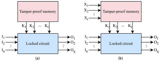
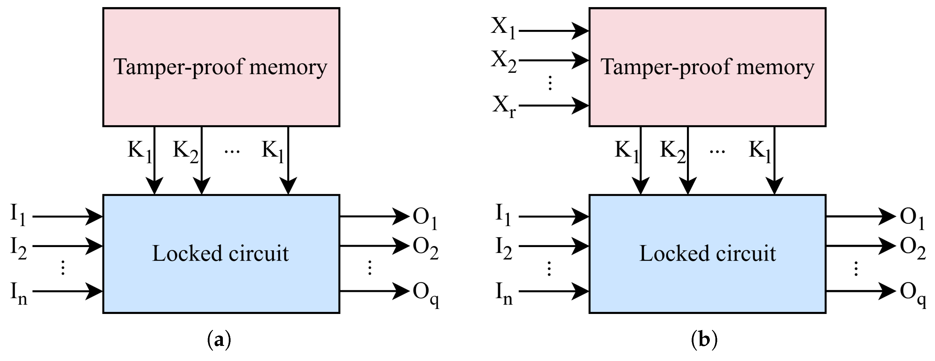
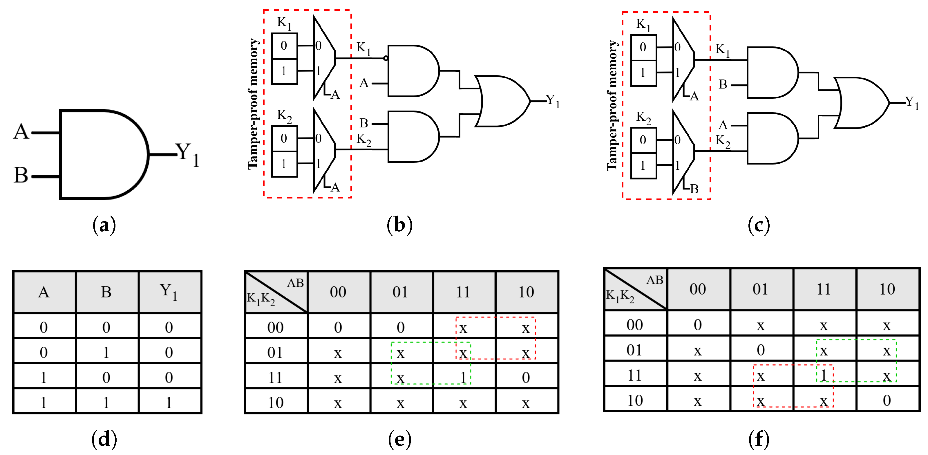
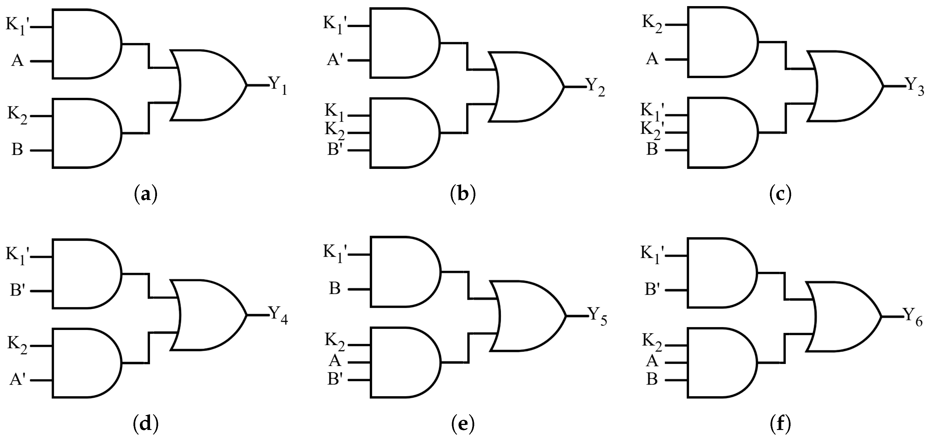
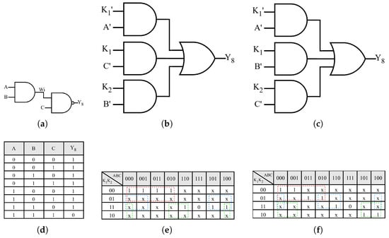
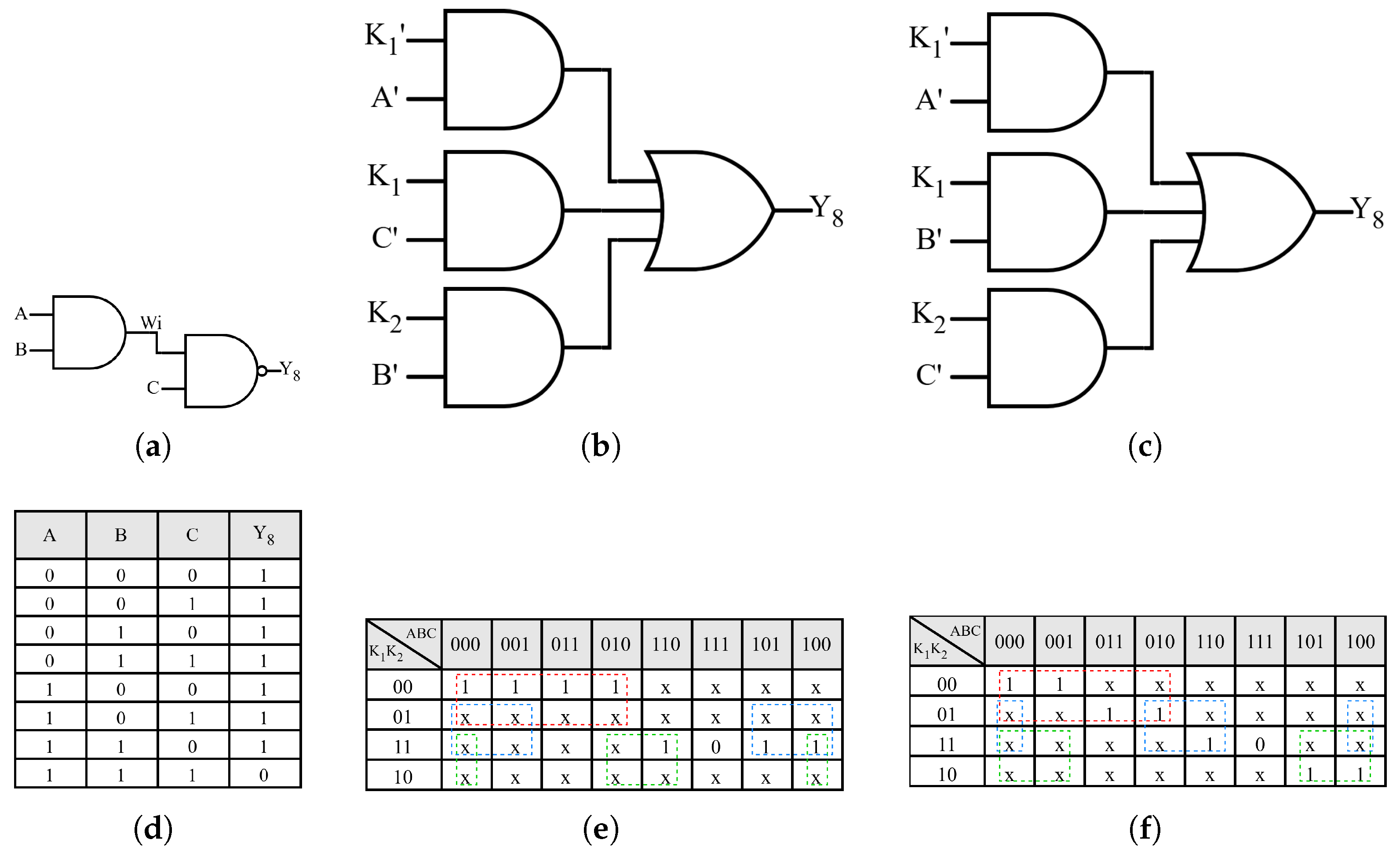
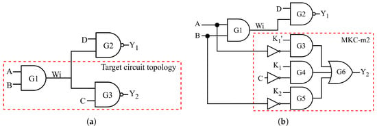
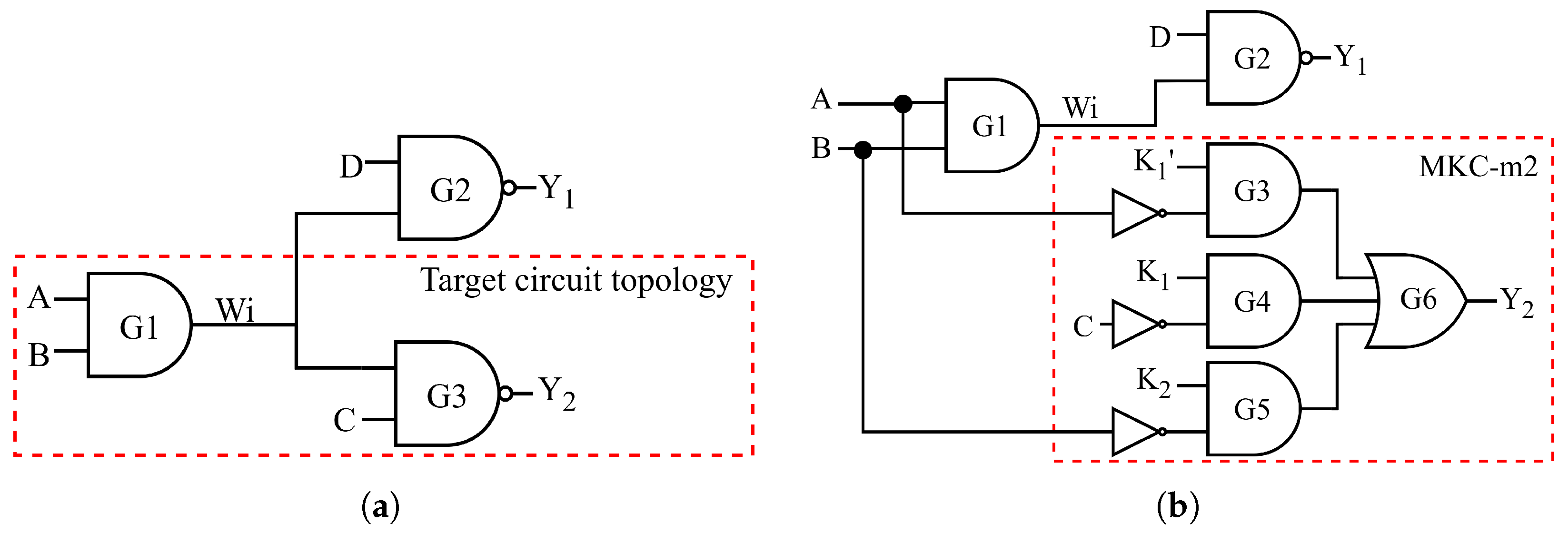

Disclaimer/Publisher’s Note: The statements, opinions and data contained in all publications are solely those of the individual author(s) and contributor(s) and not of MDPI and/or the editor(s). MDPI and/or the editor(s) disclaim responsibility for any injury to people or property resulting from any ideas, methods, instructions or products referred to in the content. |
© 2026 by the authors. Licensee MDPI, Basel, Switzerland. This article is an open access article distributed under the terms and conditions of the Creative Commons Attribution (CC BY) license.