


Abstract
The development of multifunctional and lightweight materials is increasingly shaping the design of next-generation sensing and communication systems for space applications. In CubeSat platforms, severe constraints on mass, volume, and structural complexity motivate the integration of antenna functionalities directly onto load-bearing structures. In this context, printed electronics, particularly inkjet-printed conductive materials, offer new opportunities for creating adaptive, flexible, and structure-integrated devices that support both sensing and communication functionalities. This work investigates the electrical performance of inkjet-printed conductive materials for structure-integrated patch antennas. Two silver-based inks and one carbon-based ink were deposited on fiberglass-reinforced epoxy substrates and electrically characterized over a temperature range from −20 °C to 50 °C, representative of CubeSat operational conditions. The silver-based inks exhibited electrical conductivities in the range of 106 S/m with limited variation (<10%) under thermal cycling, whereas the carbon-based ink remained below 101 S/m, even after multilayer deposition, indicating insufficient performance for this application. Based on these results, the best-performing silver ink was selected to fabricate a proof-of-concept patch antenna directly on an S2-glass/epoxy structural substrate. The proposed approach demonstrates the feasibility of integrating conductive inkjet-printed layers onto composite structural substrates intended for future structure-integrated antenna applications in CubeSat platforms, offering a pathway toward mass-efficient, low-profile, and highly integrated communication structures.
1. Introduction
In recent years, CubeSats have gained significant attention due to their reduced size, short development cycles, and cost-effectiveness, enabling a wide range of applications such as Earth observation, communications, and scientific missions [1,2,3]. However, their limited volume imposes some limitations on the integration of communication subsystems, making antenna design an important task. Efficient solutions must balance performance, compactness, mechanical robustness, and compatibility with the space environment [2,4].
Traditionally, deployable antennas such as whips have been used, but they introduce increased mass, complexity, and risk of failure, with deployment issues potentially leading to complete communication loss [2,4]. On the other hand, patch antennas have proven to be good candidates because of their low profile, easy manufacturing process, and the ability to incorporate them directly into the structure of CubeSats. A patch antenna consists of a conductive patch placed on one side of a dielectric substrate, with a ground plane on the opposite side. These antennas are lightweight, compact, and usually made of copper due to its high electrical conductivity. Alternatively, conductive inks based on metallic or carbonaceous fillers enable additive manufacturing approaches, offering sufficient performance despite their lower conductivity. These materials exhibit lower electrical conductivity compared to copper, typically ranging from 105 to 109 S/m depending on the ink formulation and processing conditions. Conductivities above 105 S/m are generally considered adequate for efficient radiation in such antennas [5].
Gatheri et al. [2] identified patch antennas as the second-most common antenna type, largely because they eliminate the need for mechanical deployment and therefore reduce the risk of failure [2,6]. Low profile and mechanical flexibility are ensured by the typical patch thickness, which varies from a few micrometers to many tens of micrometers [6].
In this context, the substrate is a dielectric material that directly affects the electrical and mechanical performance of the antenna. Fiberglass-reinforced epoxy laminate (), stands out for its low cost, mechanical robustness, and wide availability, is usually used for prototyping and short-duration missions [7,8]. However, it presents higher dielectric loss compared to advanced materials such as Rogers RO4003C () and Duroid 5880 () [9,10,11]. Thicker substrates and reduced permittivity tend to enhance bandwidth but also affect antenna size and radiation efficiency. The substrate size tends to be slightly larger than the patch to ensure sufficient field confinement and structural support.
Besides the substrate and patch, the ground plane, either copper or aluminum material, serves as the reference conductor and reflects the radiated waves to create the directional pattern. The patch antenna can be fed by a microstrip line or a coaxial probe, which is positioned in such a way that impedance matching occurs.
Regarding fabrication, conventional fabrication processes, the conductive patch is defined on the substrate surface using subtractive manufacturing techniques. Etching is one of the most widely used methods, where unwanted copper is chemically removed to obtain the desired geometry. Milling techniques can also be applied, mechanically removing material with high precision. Additionally, chemical deposition methods allow the formation of conductive layers by selectively depositing material onto the substrate [12,13,14].
The integration of patch antennas in CubeSats has been explored through various approaches to meet miniaturization and electromagnetic efficiency requirements. Antennas are typically mounted on external satellite faces using rigid substrates such as FR-4. Patch arrays have also been reported in the literature. For example, Gunaseelan et al. [15] reported a four-patch array (~96 mm2) mounted on one CubeSat face. Other innovative approaches integrate antennas with optical systems, such as the dual-band patch embedded in an Earth-observation CubeSat optical payload demonstrated by Abulgasem et al. [16]. Flexible substrates (e.g., Kapton) have been investigated in the literature as alternative implementations, but are not yet widely adopted in operational systems [2]. However, these solutions are primarily research prototypes or proof-of-concept demonstrations, with limited evidence of adoption in operational or commercial CubeSat missions. While promising, most of these strategies add mass, mechanical interfaces, or dielectric layers to the satellite structure.
The European Space Agency (ESA), in its Science Program Technology Development Plan 2024–2026, qualifies S2-Glass reinforced epoxy (GFRP with Hexcel 913 resin) as a suitable material for external CubeSat structures [17]. S2-Glass is a high-strength, low-density fiberglass that offers good tensile strength, a high Young’s modulus, and a low coefficient of thermal expansion, providing excellent mechanical robustness and dimensional stability [18]. In addition, it exhibits good resistance to thermal and radiation effects commonly encountered in aerospace environments [19]. Its dielectric constant (relative permittivity) makes it suitable as a structural substrate for printed patch antennas, enabling direct integration of communication systems onto satellite surfaces.
Based on these characteristics, fiberglass-reinforced epoxy substrate was chosen as the test material for preliminary testing due to its low cost, mechanical robustness and common use in antenna modeling. The S2-glass reinforced epoxy composite material was chosen as a typical structural dielectric substrate because it is mechanically superior and suitable for aerospace structures. In terms of conductive materials, silver-based ink was chosen for its superior electrical conductivity and suitability for printed electronics, while carbon-based ink was chosen as an economical alternative conductive material for comparative purposes.
In recent years, advanced manufacturing techniques, such as inkjet printing, have been investigated as efficient, cost-effective, and environmentally friendly alternatives for fabricating patch antennas. Inkjet is a non-contact, additive deposition technology capable of dispensing picolitre-scale droplets with high positional accuracy, enabling fine-feature patterning without masks or resists, which reduces material waste and process steps [20,21]. Compared to screen printing (which requires stencils and is limited in resolution) and aerosol jet printing (which requires more complex equipment and gas-focusing systems), inkjet offers an excellent balance of resolution, versatility, and compatibility with a wide range of substrates, including flexible and rigid dielectrics. Furthermore, inkjet is scalable and has been validated in the literature for antenna fabrication on FR-4 substrates. Several experimental works have demonstrated the viability of inkjet-printed antennas. Goh et al. [22] successfully fabricated patch antennas using silver nanoparticle ink deposited via drop-on-demand (DOD) inkjet on FR-4. Popela et al. [8] compared fully additively manufactured patch antennas (with silver inks) to traditional etched antennas on FR-4 and Arlon 25N, confirming comparable performance and highlighting the practical benefits of fully additive fabrication. Nascetti et al. [7] presented a high-efficiency S-band patch for CubeSats using FR-4, demonstrating a lightweight and low-profile solution for Earth-observation missions.
Building on these previous developments, conventional substrates such as FR-4, which are not intended to provide structural support, are replaced by structural dielectric materials like S2-Glass. This design enables the CubeSat panel to simultaneously function as both a mechanical support and an antenna substrate. It also eliminates the need for additional PCBs and fasteners, resulting in significant mass reduction and simplified integration, in line with current trends toward miniaturization and multifunctional structures in CubeSats.
This study aims to assess the feasibility of integrating inkjet-printed conductive materials onto structural dielectric substrates for future structure-integrated antenna applications in CubeSat platforms by investigating the effect of temperature variations on their electrical conductivity under representative operational conditions. The present work focuses on the electrical and thermal assessment of conductive inkjet-printed materials intended for future structure-integrated antenna applications. Therefore, the study is centered on material-level electrical characterization, thermal stability, and process feasibility rather than complete RF antenna performance validation. The antennas are made using conductive inks, two based on silver and one based on carbon, printed on a fiberglass-reinforced epoxy substrate. By comparing both materials, we aim to find which ink performs better electrically and could be directly integrated into structural dielectric substrates such as S2-Glass, to reduce overall CubeSat mass. The best-performing ink was then used to fabricate a proof-of-concept antenna on an S2-Glass substrate, demonstrating its potential for direct integration into the satellite structure.
2. Materials and Methods
The fabrication and characterization procedures were conducted to evaluate the electrical performance of inkjet-printed patch antennas manufactured with three different conductive inks, including silver-based and carbon-based formulations, deposited on fiberglass-reinforced epoxy substrates. The following subsections describe the materials, printing setup, process parameters, and measurement methods adopted in this study.
2.1. Substrates
Two dielectric substrates were considered in this work: a commercial fiberglass-reinforced epoxy substrate used for the main experimental study, and an S2-glass reinforced epoxy resin. The fiberglass-reinforced epoxy substrate with a thickness of 1.5 mm was chosen for the conductive inks’ comprehensive electrical characterization. In contrast, the 0.8 mm S2-glass/epoxy laminate was produced in-house and used exclusively as a structural proof-of-concept demonstrator. The substrate thicknesses were determined using a digital micrometer at multiple locations to ensure dimensional consistency across the samples. Since substrate thickness directly influences antenna resonant frequency, impedance matching, and bandwidth, no direct RF performance comparison between the two configurations is intended in this study. The demonstrator was included to validate the feasibility of integrating conductive inks onto a representative structural composite substrate for future CubeSat applications.
2.2. Conductive Inks
Three conductive inks were evaluated in this study to assess their suitability for inkjet printing and their electrical behavior under varying temperatures. The main physical properties of the inks, namely viscosity, density, and surface tension, are summarized in Table 1.
Table 1.
Characteristics of different inks.
All inks were used as received, without further dilution or modification, to preserve their original formulation and ensure reproducibility. Before printing, the inks were homogenized to minimize particle sedimentation and ensure consistent dispensing throughout the printing process using an ultrasonic bath following the supplier’s recommendations.
To evaluate whether the selected inks exhibited suitable properties for inkjet deposition, the Reynolds number (Re), Ohnesorge number (Oh), and inverse Ohnesorge number, also referred to as the printability parameter (Z), were calculated. These dimensionless parameters describe the balance between inertial, viscous, and surface tension forces during droplet formation in Drop-on-Demand (DOD) inkjet printing:
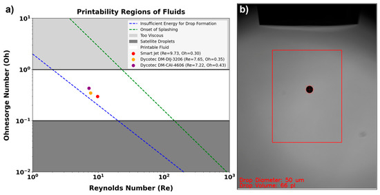
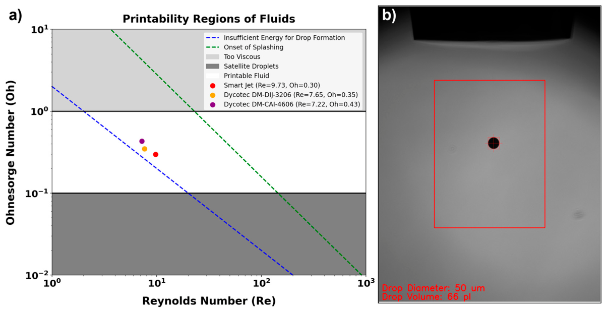
where () is the ink density, () is the droplet velocity, () is the nozzle diameter or characteristic droplet diameter, () is the dynamic viscosity, and () is the surface tension of the ink. Stable inkjet printing is generally associated with (1 < Z < 10), corresponding to droplet formation without excessive viscous damping, splashing, or satellite droplets. Based on the calculated values, all inks fall within the printable regime of the standard inkjet operating map (Figure 1a) allowing the formation of stable droplets (Figure 1b).
Figure 1.
(a) Printability map in the Reynolds–Ohnesorge space, showing the printable regions and the operating points of the studied inks and (b) example of a droplet inside the red box and its diameter (50 µm) and volume (60 pL).
2.3. Inkjet Printing Setup
The deposition of the antennas was performed using the Microdrop Autodrop Gantry II system equipped with an MD-K-130 printhead (microdrop Technologies GmbH, Norderstedt, Germany) featuring a 50 µm nozzle, able to process inks in a viscosity range of 0.4–20 mPa·s. The DOD actuation is based on a piezoelectric transducer that enables the controlled ejection of individual picolitre-scale droplets. Throughout the printing process, the actuation frequency was maintained at 500 Hz to ensure stable and repeatable droplet generation. Optimal printing conditions are achieved when the droplet diameter closely matches the nozzle diameter.
The first step involved calibrating the ejection of a single droplet. The process involved adjusting the driving voltage and pulse width until achieving:
- ▪
- Droplet diameter ≈ 50 µm;
- ▪
- Drop velocity ≈ 2 m/s;
- ▪
- Stable and consistent droplet formation within an appropriate frequency range.
A stroboscopic camera integrated into the printing system was used to observe droplet shape and trajectory (Figure 1b).
2.4. Printing Process Optimization Methodology
The optimization process comprised several steps, including selection of the optimal operating frequency, evaluation of the nozzle–substrate distance, optimization of machine cleaning procedures before and after deposition, and adjustment of ultrasonic bath time to ensure proper particle dispersion. For each ink, the optimal voltage and pulse length were determined to achieve stable droplet formation and uniform deposition. In addition, deposition patterns, p-value, and y-direction spacing were systematically investigated. Before deposition, the fiberglass-reinforced epoxy substrates were mechanically prepared by sanding and polishing to improve surface uniformity. Subsequently, the substrates were cleaned with acetone to remove surface contaminants and enhance ink adhesion.
The printing parameters were separately optimized for each ink to achieve stable droplet generation, reduce satellite droplet generation, and obtain uniform conductive lines after printing. The chosen parameters resulted in stable droplets with diameters of about 50 µm. The optimal values of the parameters used for the fabrication of the conductive patches are presented in Table 2.
Table 2.
Printing parameters optimized for each ink.
The chosen spacing between drops was roughly half the size of the diameter of the droplets, favoring controlled overlapping of the droplets as well as the creation of a continuous film. A larger spacing would lead to discontinuous printed lines, while a smaller one would cause more accumulation and spreading of the ink. The chosen p-value, therefore, offered a balance between film continuity, dimensional accuracy, and surface uniformity.
During printing, the inkjet printing plate was maintained at 50 °C to ensure thermal stability and controlled solvent evaporation. The temperature was also controlled on the surface of the fiberglass-reinforced epoxy samples, which reached approximately the same temperature of 50 °C for the ink deposition, ensuring consistent printing conditions. The deposition was carried out with a drop spacing corresponding to half of the droplet diameter along both the x- and y-axes, resulting in controlled droplet overlapping and improved film continuity.
The quality of the conductive printed films was assessed using a series of tests, including visual examination, observation of droplets using an integrated strobe light camera, determination of film thickness using the Bruker Dektak XT profiler (Bruker, Billerica, MA, USA), measuring electrical conductivity using the four-point probe technique, and checking the homogeneity using the coefficient of variation (CV), measured in various areas of the printed films. In addition, an adhesion test based on the ASTM D3359-23 standard [23] was carried out to assess the mechanical integrity of the printed films on the substrate.
Layer thickness optimization was performed by adjusting the number of printed layers and droplet spacing. This was done using a trade-off condition between high conductivity, connectivity, and homogeneity. Increasing the number of layers usually resulted in high conductivity due to the formation of more conductive layers, although excessive thickness reduced film uniformity. Therefore, the optimum thickness varied depending on the composition of the conductive ink used and could be determined based on conductivity and CV measurements.
2.5. Electrical Characterization
The electrical properties of the printed patches were measured using a 4-point probe with 0.01 m between the middle electrodes connected to a Keithley 2410-C 1100 V SourceMeter (Keithley Instruments, Solon, OH, USA). The electrical resistance of the samples was characterized over a temperature range from −20 °C to 50 °C using a controlled climatic test chamber (Nüve ID 301, Nüve Sanayi Malzemeleri İmalat ve Ticaret A.Ş., Ankara, Turkey). This temperature range represents realistic operational conditions for RF subsystems, like thermal vacuum cycling tests used in CubeSat thermal validation exercises, while avoiding damage to non–pace-qualified materials and measurement equipment [24]. The sample temperature was continuously monitored using a type-K thermocouple placed in direct contact with the printed surface and connected to an OM-CP-OCTPRO Omega data logger (Omega Engineering, Norwalk, CT, USA), ensuring accurate temperature correlation during the measurement. The conductivity (σ) was then calculated using the equation:
where t is the average film thickness, measured by the step-height method using a Bruker Dektak XT contact profilometer (i.e., the height difference between the printed film surface and an adjacent uncoated reference region of the substrate), R is the measured electrical resistance, w is the width of the conductive pattern, and L is the distance between the middle electrodes of the 4-point probe.
Since conductivity measurements were performed at three different regions of each printed sample, the mean conductivity, standard deviation, and coefficient of variation were calculated to evaluate the spatial homogeneity of the printed conductive layers:
where () is the conductivity measured at each region of the printed sample, () is the mean conductivity and (N) is the total number of measurement regions considered for each sample.
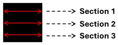
Based on the literature, the electrical conductivity of the printed patches should lie in the range of 105 to 109 S/m [5]. To evaluate the spatial uniformity of the printed films, measurements were taken at three distinct regions of each printed patch (Sections 1–3), as illustrated in Figure 2. This procedure was consistently applied to all samples and layer configurations to ensure reliable comparison between inks and printing conditions.
Figure 2.
Scheme of the three distinct regions of each printed patch.
The homogeneity of the patch along the measured sections was evaluated at room temperature using the coefficient of variation (CV) of the conductivity data across the different regions, according to the following equation:
where SD is the standard deviation and is the mean.
2.6. S2-Glass Substrate Production and Mechanical Characterization
For the substrate production, S2-Glass fiber supplied by Fysol, Chambéry, France, was combined with LY3508 epoxy resin using a laboratory drum winder to prepare unidirectional pre-impregnated materials. The prepregs were then stored at room temperature for 24 h to achieve the B-stage and then cooled down to −18 °C to delay polymerization reactions. Finally, the prepreg sheets were cut into smaller sections and laminated in a 6-layer quasi-isotropic stacking sequence [0/90/+45/−45/90/0] for patch antenna production and a six-layer UD laminate for mechanical testing. The laminates were consolidated into GFRP composites using an autoclave at 120 °C and 3.5 bar for 4 h.
The UD laminates were then cut into specimens for tensile testing at 0° according to ASTM D3039M [25] and the glass fiber volume fractio (Vgf) of the laminate was determined in accordance with ASTM D3529M [26].
3. Results
3.1. Genesink Smart Jet C47NJET10020
The Genesink Smart Jet C47NJET10020 (Genesink, Rousset, France) was first characterized to assess its electrical performance and homogeneity. Rectangular conductive patches with dimensions of 0.022 m × 0.016 m were fabricated using one- and two-layer printing configurations. Table 3 summarizes the measured film thicknesses, mean electrical conductivity values (using Equation (5)), and coefficients of variation obtained at room temperature.
Table 3.
Conductivity Uniformity Analysis Across Printed Patch Sections.
Homogeneity was evaluated using the coefficient of variation (CV%), which quantifies relative dispersion and is scale-independent. Unlike absolute measures of spread, the CV enables direct comparison of variability across layer configurations, even when conductivity levels differ. Moreover, the CV does not require normality assumptions and, in this context, reflects the spatial variability of conductivity within a printed sample rather than measurement uncertainty. The results are presented in Table 3.
The improved homogeneity observed for the two-layer samples can be attributed to the inkjet printing process, where the second conductive layer compensates for local thickness variations and defects present after the first pass. This results in enhanced particle connectivity and a more uniform conductive path across the surface.
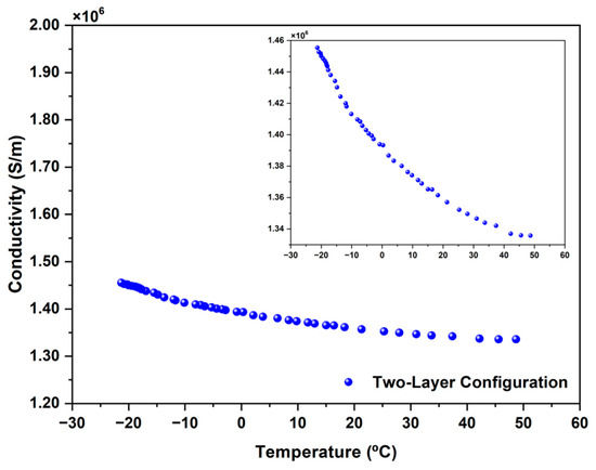
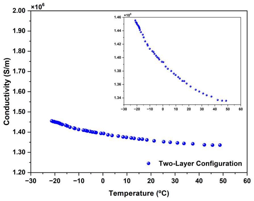
From these results, it can also be observed that, at room temperature, the conductivity is in the order of S/m. To better approximate space-like conditions, the patch antenna was subsequently tested under more extreme environments using a climatic chamber, within a temperature range from −20 °C to 50 °C. The graph in Figure 3 illustrates the conductivity behavior as a function of temperature.
Figure 3.
Conductivity behavior as a function of temperature for the Genesink Smart Jet C47NJET10020 ink.
A slight decrease in conductivity with increasing temperature was observed, with values ranging from approximately S/m at low temperatures to S/m at higher temperatures. This corresponds to a relative variation of about 10% over a temperature span of nearly 70 °C. This behavior is consistent with metallic conduction mechanisms, where increased lattice vibrations reduce charge carrier mobility [27]. However, the limited magnitude of this variation indicates good thermal stability, and such changes are not expected to significantly affect patch antenna performance under operational conditions.
3.2. Dycotec DM-SIJ-3206
Using the Dycotec DM-SIJ-3206 silver ink (Dycotec Materials, Calne, UK), three patches were fabricated: with one, two and three printed layers. The third layer was added to analyze a possible increase in homogeneity as observed for the two-layer patch with the Genesink Smart Jet C47NJET10020 ink. All three patches were produced with a length of 0.011 m and a width of 0.01 m. Table 4 presents the conductivity values obtained at room temperature. The corresponding conductivity values were calculated using Equation (5).
Table 4.
Summary of the conductivity values for the one-, two-, and three-layer configurations.
The results shown in Table 4 indicate that increasing the number of printed layers enhances electrical conductivity due to improved percolation and interlayer connectivity. However, while samples with one and two layers exhibit low CV values (≈8–9%), indicating higher electrical homogeneity, the three-layer configuration shows a significantly higher CV (21.8%). This increased variability suggests reduced uniformity, likely associated with cumulative printing effects such as ink spreading, layer misalignment, thickness variation, or incomplete sintering between stacked layers. These results highlight a trade-off between higher conductivity and spatial homogeneity as the number of layers increases. Nevertheless, the increase in the number of printed layers always improves conductivity. This demonstrates that there is a need to optimize the parameters to achieve uniform homogeneity and stability on the final patch. The results have demonstrated that while multilayer printing is important for conductivity, the conditions for fabrication need to be controlled.
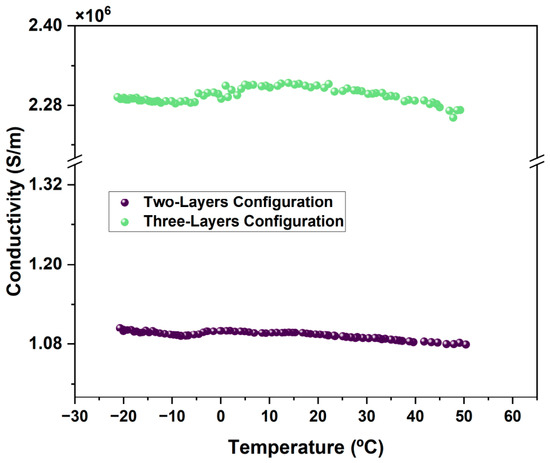
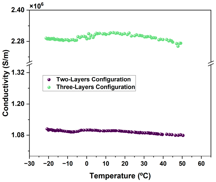
Considering the patch as a whole, using the average conductivity for each layer, a clear increase is observed with the number of printed layers. In particular, the conductivity increases by approximately 44% from one to two layers, and by 58% from two to three layers. Although the three-layer configuration exhibits a substantially higher CV, indicating increased spatial variability, all samples remain within the same order of magnitude. Both two- and three-layer samples present consistently high electrical conductivity predominantly on the order of . Therefore, temperature-dependent tests were performed for the two- and three-layer configurations, as they represent the most electrically conductive cases. The patch antennas were subsequently characterized under more extreme environments, within a temperature range from −20 °C to 50 °C. The conductivity behavior as a function of temperature is presented in Figure 4.
Figure 4.
Conductivity behavior as a function of temperature for the two- and three-layer configurations of Dycotec DM-SIJ-3206 silver ink.
3.3. Dycotec DM-CAI-4606
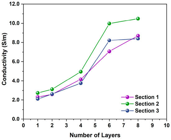
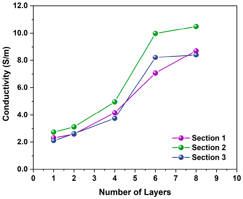
The Dycotec DM-CAI-4606 ink, a carbon-based conductive formulation, was also evaluated as a potential candidate for inkjet-printed patch antennas. Due to the behavior of this ink, patches with 1 to 8 layers were printed with 0.014 m in length and 0.012 m in width. Figure 5 summarizes the conductivity values obtained for samples printed with one, two, four, six, and eight layers of the DM-CAI-4606 ink. A clear and consistent increase in electrical conductivity is observed as the number of printed layers increases.
Figure 5.
Conductivity behavior as a function of the number of layers for the Dycotec DM-CAI-4606 ink.
Table 5 presents the mean conductivity, thickness, and coefficient of variation in the patches fabricated with this ink for different numbers of printed layers.
Table 5.
Summary of the conductivity values for all layer configurations.
Unlike silver-based inks, where electrical conduction is dominated by metallic continuity, carbon-based inks rely on percolation mechanisms between conductive particles, making their electrical properties strongly dependent on film thickness and structural homogeneity. In single-layer samples, the measured electrical conductivity is on the order of a few S/m, indicating that only a limited conductive network is formed, with poor interparticle connectivity. This suggests that the system operates below or near the percolation threshold, where charge transport is dominated by tunneling and hopping mechanisms rather than continuous conductive pathways. As the number of printed layers increases to two and four, a gradual and consistent increase in conductivity is observed, which can be attributed to improved particle overlap and progressive reduction in microstructural discontinuities within the printed film.
Conductivity increases with the number of printed layers. In particular, the average conductivity increases by approximately 16% from one to two layers, 54% from two to four layers, 96% from four to six layers, and 9% from six to eight layers. Nevertheless, the conductivity values remain within the same order of magnitude, suggesting that the improvement is mainly due to densification and enhancement of existing conductive pathways rather than the formation of a new conduction regime. However, the evolution is not strictly gradual. A pronounced increase in conductivity is observed between four and six layers, indicating a significant enhancement in the connectivity of the conductive network, likely associated with the system approaching the percolation threshold.
Further increasing the number of layers to eight results in a slight improvement in conductivity, indicating that the conductive network is approaching a well-established state. At this stage, most conductive pathways are already formed, so adding more material has a limited effect. Although conductivity continues to increase, the improvement becomes progressively smaller with each additional layer. This behavior is consistent with nanoparticle-based conductive inks, where electrical transport depends on the formation of connections between particles. As more layers are added, particles become more densely packed, increasing the number of contact points and conductive paths. However, once a well-connected network is formed, additional material mainly reinforces existing paths rather than creating new ones, leading to smaller gains in conductivity [28].
It is also important to mention that the obtained thickness does not increase with the increasing number of printed layers in a monotonic way. This is caused by certain features of the inkjet printing technique, during which droplets may be distributed irregularly and dry unevenly. It implies that not all layers add up equally to the thickness.
In summary, although multilayer deposition of the Dycotec DM-CAI-4606 carbon-based ink led to a progressive increase in electrical conductivity, the maximum achieved values remained several orders of magnitude below those required for efficient patch antenna operation [5]. Consequently, this ink formulation is deemed unsuitable for structure-integrated patch antennas intended for CubeSat communication systems.
3.4. Adhesion Tests
Adhesion performance was tested by using a cross-cut tape test, which was carried out following ASTM standard D3359-23, Method B [23]. Fiberglass-reinforced epoxy substrates coated with conductive ink (Genesink Smart Jet C47NJET10020, Dycotec DM-SIJ-3206 and Dycotec DM-CAI-4606) were used for the test. A lattice cut was made to penetrate the coating down to the substrate material using a scalpel. Pressure-sensitive adhesive tape was placed over the lattice and pressed evenly before being peeled off at nearly 180°. The adhesion was qualitatively classified according to the ASTM scale (0B–5B). Table 6 summarizes the obtained adhesion ratings.
Table 6.
Cross-cut adhesion test results.
For the Genesink Smart Jet C47NJET10020, the cross-cut test showed no observable coating detachment after tape removal, corresponding to a 5B classification, which indicates excellent adhesion of the printed conductive film to the fiberglass-reinforced epoxy substrate. Similarly, the Dycotec DM-SIJ-3206 ink also exhibited a 5B classification, with no visible detachment in the cross-cut area. This result indicates excellent adhesion, comparable to that of the Genesink ink, suggesting strong interfacial bonding between the printed film and the substrate. The Dycotec DM-CAI-4606 ink exhibited a 4B classification, indicating minor coating detachment at the intersections of the cuts. This suggests good adhesion to the fiberglass-reinforced epoxy substrate, although slightly inferior to that of the silver-based inks. The observed detachment at the intersections could be attributed to lower cohesion within the carbon-based film or weaker interfacial bonding with the substrate than with the silver ink.
3.5. Mechanical Characterization of the S2-Glass GFRP Laminate
The mechanical characterization of the S2-glass fiber UD laminate was performed in an Instron 5900R with a 200KN load cell, with the strain acquired by an external stereo DIC system. The produced S2-glass laminate presented a tensile stress of 1314 ± 20 MPa with a Young’s Modulus of 41.9 ± 1.8 GPa and a tensile strain of 3.4 ± 0.13% with a Poisson’s ratio of 0.32 ± 0.03. The laminate presented 51.6 ± 2.8% of GF volume fraction with porosity ranging up to 4%. These results demonstrate the applicability of this material for a structural component of a CubeSat, greatly improving on the standard FR4 material commonly used in patch antennas, which presents a tensile strength of 320 MPa [29]. Mechanical properties in the transverse (90°) direction were not experimentally determined in this study. As these properties are strongly influenced by matrix behavior and fiber volume fraction, they were not considered critical for the present demonstrator-focused validation.
3.6. Proof-of-Concept Structural Demonstrator
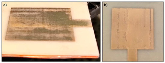
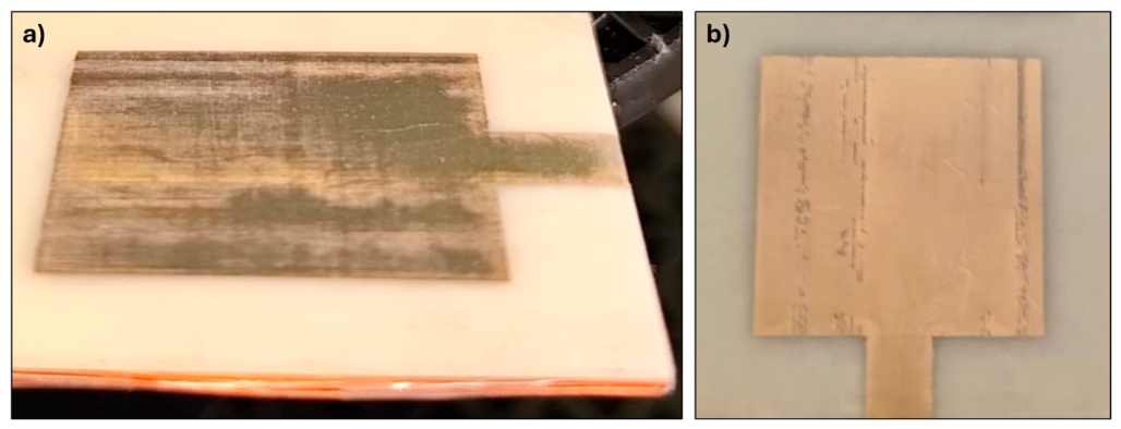
Following the electrical characterization, a proof-of-concept structural demonstrator was created to explore the feasibility of using the printed conductive ink when integrated into a representative structure. This prototype was designed using Dycotec DM-SIJ-3206 conductive ink, printed in two layers on an S2-glass reinforced epoxy resin substrate (Figure 6). The choice of this design was made according to the conductivity results that were obtained in the earlier section while considering the limitations of the process and materials.
Figure 6.
Antenna demonstrator: (a) the copper ground plane on the substrate is visible and the (b) top view of the patch printed with conductive ink.
The material characterization was focused on electrical conductivity measurements (Table 7), as this parameter directly reflects the ability of the printed structure to support current flow and is therefore a key factor in determining performance in antenna-related applications.
Table 7.
Mean electrical conductivity values for the different sections of the demonstrator.
4. Discussion
This study investigated how ink formulation and print stacking govern the electrical suitability of inkjet-printed conductors for structure-integrated CubeSat patch antennas.
The clear performance gap between silver- and carbon-based inks arises from their distinct conduction mechanisms. Silver inks readily achieve metallic conduction once a continuous network is formed, enabling conductivities compatible with efficient radio-frequency radiation. In contrast, the carbon-based ink relies on percolation and tunneling between particles and does not reach a fully continuous conductive regime, even with multilayer deposition. After the deposition of eight layers, the conductivity of the carbon ink remained well below the level required for our application (≤105). This inherently limits its suitability for structure-integrated antennas, indicating that material choice is a primary feasibility constraint.
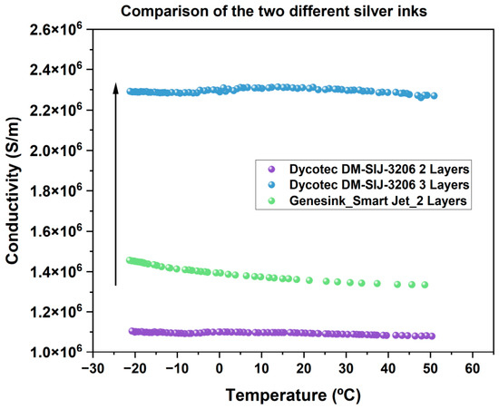
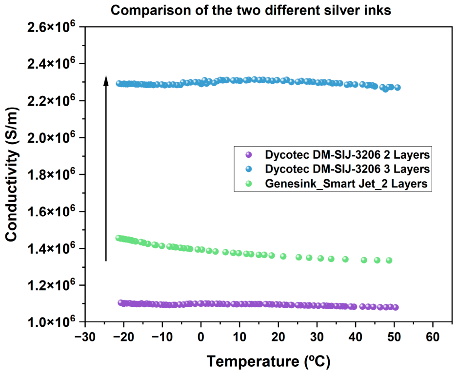
Increasing the number of printed layers generally improves conductivity by enhancing interparticle connectivity and mitigating local defects. However, higher layer counts can also introduce increased spatial variability due to cumulative printing effects. For patch antennas, where uniform current distribution is critical to radiation efficiency and impedance stability, maximizing conductivity alone is insufficient. An intermediate configuration, such as a two- or three-layer silver ink deposition, represents a balanced compromise between electrical performance and homogeneity. The graph in Figure 7 shows a clear comparison between the two silver inks.
Figure 7.
Comparison between the two different silver inks.
Among the tested samples, the Dycotec DM-SIJ-3206 ink exhibited the highest conductivity values, reaching approximately 2.3 × 10⁶ S/m for three printed layers, while maintaining good stability across the temperature range. The two-layer configuration of the same ink shows lower conductivity, around 1.1 × 10⁶ S/m, confirming the positive impact of increasing the number of deposited layers. The Genesink Smart Jet ink presented intermediate performance, with conductivity values around 1.4 × 10⁶ to 1.5 × 10⁶ S/m for two layers, but with a slightly more pronounced decrease as temperature increased.
The observed minor reduction in conductivity with temperature is consistent with the typical behavior of metallic conductors, resulting from increased lattice vibrations that slightly hinder charge carrier mobility [30,31]. However, the overall conductivity variation remains limited, staying below 10% across the considered temperature range. For most practical applications, including patch antennas, this variation does not compromise the antenna’s performance.
In addition to electrical characterization, adhesion tests were performed to assess the mechanical robustness of the printed layers. The results confirmed good adhesion of the inks to the substrate, with no significant delamination or degradation observed, reinforcing its suitability for space-related applications where mechanical and thermal stresses are critical.
Based on the overall results obtained, the Dycotec DM-SIJ-3206 ink demonstrated superior electrical performance and was identified as the most suitable candidate for future inkjet-printed antenna-related applications in CubeSat platforms. Consequently, a demonstrator using the S2-Glass substrate was fabricated employing a patch antenna with two printed layers of this Dycotec silver ink. Although not corresponding to the optimal configuration identified, this implementation enables validation of the inkjet printing process and confirms the suitability of the conductive material for antenna applications. The two-layer configuration was selected in preference to the three-layer optimum because it offers the best balance between electrical conductivity (~1.1 × 10⁶ S/m) and spatial homogeneity (CV~8.2%), whereas the three-layer configuration, while achieving higher conductivity (~2.3 × 10⁶ S/m), exhibited a substantially elevated CV of 21.8%, indicating reduced uniformity that could compromise antenna radiation performance. For a demonstrator whose primary purpose is to validate printability and ink–substrate compatibility, the more homogeneous two-layer configuration was therefore the more appropriate choice.
5. Conclusions
This work demonstrates the feasibility of inkjet-printing conductive materials onto structural composite substrates intended for future structure-integrated antenna applications in CubeSat platforms. Among the investigated materials, the silver-based inks achieved electrical conductivities on the order of 106 S/m with limited sensitivity to temperature variations between −20 °C and 50 °C, confirming their suitability for the envisioned applications. In contrast, the carbon-based ink exhibited conductivities several orders of magnitude lower, even after multilayer deposition, rendering it unsuitable for efficient antenna operation.
The successful fabrication of a proof-of-concept antenna directly on an S2-glass/epoxy structural substrate highlights the potential of combining mechanical and electromagnetic functionalities within a single component. This approach enables mass and volume savings while simplifying system integration, contributing to the development of lightweight, low-profile, and multifunctional communication subsystems for future CubeSat missions.
Several directions are identified for future work. Full electromagnetic characterization of the fabricated antenna, including return loss, radiation pattern, gain, and radiation efficiency, is required to validate the RF performance of the printed conductors and constitutes the immediate next step of this research. Additionally, a dedicated design-of-experiments approach would enable the derivation of empirical models that formally quantify the relationship between key printing parameters (voltage, pulse width, drop spacing, and number of layers) and the resulting electrical conductivity, supporting process optimization for future antenna designs. Finally, mechanical testing of the printed laminates after thermal cycling would further validate the long-term structural and functional integrity of the structure-integrated antenna concept under representative CubeSat operational conditions.
Author Contributions
Conceptualization, F.R., D.G. and A.A.; methodology, F.R. and D.G.; validation, F.R., D.G. and J.V.; formal analysis, F.R.; investigation, F.R., D.G. and C.C.; resources, J.V., A.A. and J.d.S.R.; data curation, F.R.; writing—original draft preparation, F.R.; writing—review and editing, D.G., J.V., J.d.S.R. and A.A.; visualization, F.R.; supervision, A.A. and D.G.; project administration, A.A.; funding acquisition, A.A. All authors have read and agreed to the published version of the manuscript.
Funding
This research received no external funding.
Institutional Review Board Statement
Not applicable.
Informed Consent Statement
Not applicable.
Data Availability Statement
The original contributions presented in this study are included in the article. Further inquiries can be directed to the corresponding author.
Acknowledgments
We would like to acknowledge Fysol for providing the dry S2-glass fiber used to prepare the GFRP composite substrate.
Conflicts of Interest
The authors declare no conflicts of interest.
References
- NASA. What Are Smallsats and CubeSats? Available online: https://www.nasa.gov/what-are-smallsats-and-cubesats/ (accessed on 10 December 2025).
- Ghaderi, M.R.; Amiri, N. CubeSat Antenna Designs in the Last 2 Decades (2002–2023): A Survey. Int. J. Aeronaut. Space Sci. 2025, 26, 327–375. [Google Scholar] [CrossRef] [Scilit]
- ESA Technology CubeSats. 2023. Available online: https://www.esa.int/Enabling_Support/Space_Engineering_Technology/Technology_CubeSats/ESA_Technology_CubeSats (accessed on 10 December 2025).
- Liu, S.; Theoharis, P.I.; Raad, R.; Tubbal, F.; Theoharis, A.; Iranmanesh, S.; Abulgasem, S.; Khan, M.U.A.; Matekovits, L. A Survey on CubeSat Missions and Their Antenna Designs. Electronics 2022, 11, 2021. [Google Scholar] [CrossRef] [Scilit]
- Lin, Y.-X.; Ko, K.-Y.; Lai, F.-P.; Chen, Y.-S. Inkjet-Printed Reflectarray Antenna Integrating Feed and Aperture on a Flexible Substrate Using Origami Techniques. Electronics 2024, 13, 2505. [Google Scholar] [CrossRef] [Scilit]
- Almeida, T.A.S. Planar Antennas for CubeSat Missions. Master’s Thesis, Instituto Superior Técnico, Lisboa, Portugal, 2018. [Google Scholar]
- Nascetti, A.; Pittella, E.; Teofilatto, P.; Pisa, S. High-Gain S-Band Patch Antenna System for Earth-Observation CubeSat Satellites. IEEE Antennas Wirel. Propag. Lett. 2015, 14, 434–437. [Google Scholar] [CrossRef] [Scilit]
- Popela, M.; Olivová, J.; Plíva, Z.; Petržílka, L.; Krchová, M.; Joska, Z.; Janů, P. A Novel Approach to the Production of Printed Patch Antennas. Appl. Sci. 2024, 14, 1556. [Google Scholar] [CrossRef] [Scilit]
- Isola Group. FR408 Laminate and Prepreg Data Sheet. 2024. Available online: https://www.isola-group.com/wp-content/uploads/data-sheets/fr408-laminate-and-prepreg.pdf?t=1244069 (accessed on 25 November 2025).
- Rogers Corporation. RO4000 Series Laminates—RO4003C and RO4350B Data Sheet. 2018. Available online: https://rogerscorp.com (accessed on 25 November 2025).
- Rogers Corporation. RT/Duroid 5870/5880 High Frequency Laminates—Data Sheet. 2022. Available online: https://www.rogerscorp.com/-/media/project/rogerscorp/documents/advanced-electronics-solutions/engl (accessed on 25 November 2025).
- Balanis, C.A. The Microstrip Antenna. In Antenna Theory: Analysis and Design; Wiley: Hoboken, NJ, USA, 1996. [Google Scholar]
- Kumar, G.; Ray, K.P. Broadband Microstrip Antennas; Artech House Antennas and Propagation Library; Artech House: Boston, MA, USA; London, UK, 2003. [Google Scholar]
- Garg, R.; Bhartia, P.; Bahl, I.; Ittipiboon, A. Microstrip Antenna Design Handbook; Artech House: Boston, MA, USA; London, UK, 2001. [Google Scholar]
- Gunaseelan, S.; Murugan, M. High Gain Patch Antenna for CubeSat. In Proceedings of the 2016 International Conference on Wireless Communications, Signal Processing and Networking (WiSPNET); IEEE: Chennai, India, 2016; pp. 52–54. [Google Scholar]
- Abulgasem, S.; Tubbal, F.; Raad, R.; Theoharis, P.I.; Liu, S.; Ali Khan, M.U. A Wideband Metal-Only Patch Antenna for CubeSat. Electronics 2020, 10, 50. [Google Scholar] [CrossRef] [Scilit]
- Alqassab, Y.; Alharam, A.; Khater, A.; Almalki, M. Evaluation of GFRP Composite Material in CubeSats Structures; Mohammed Bin Rashid Space Centre (MBRSC): Dubai, United Arab Emirates, 2023; pp. 1–8. [Google Scholar]
- De Naoum, K.; Schadegg, J. All About Fiberglass. Xometry, 27 August 2024. Available online: https://www.xometry.com/resources/materials/what-is-fiberglass/ (accessed on 20 December 2025).
- Khan, R.A. Thermo-Mechanical Properties and Applications of Glass Fiber Reinforced Polymer Composites. Mod. Concepts Mater. Sci. 2023, 5, 1–9. [Google Scholar] [CrossRef] [Scilit]
- Zeng, X.-Y.; Tang, Y.-Q.; Cai, X.-Y.; Tang, J.-X.; Li, Y.-Q. Solution-Processed OLEDs for Printing Displays. Mater. Chem. Front. 2023, 7, 1166–1196. [Google Scholar] [CrossRef] [Scilit]
- Kholghi Eshkalak, S.; Chinnappan, A.; Jayathilaka, W.A.D.M.; Khatibzadeh, M.; Kowsari, E.; Ramakrishna, S. A Review on Inkjet Printing of CNT Composites for Smart Applications. Appl. Mater. Today 2017, 9, 372–386. [Google Scholar] [CrossRef] [Scilit]
- Goh, G.L.; Ma, J.; Chua, K.L.F.; Shweta, A.; Yeong, W.Y.; Zhang, Y.P. Inkjet-Printed Patch Antenna Emitter for Wireless Communication Application. Virtual Phys. Prototyp. 2016, 11, 289–294. [Google Scholar] [CrossRef] [Scilit]
- ASTM D3359-23; Standard Test Methods for Rating Adhesion by Tape Test. ASTM International: West Conshohocken, PA, USA, 2023.
- Seyedzadeh, A.; Okasha, M.; Alblooshi, A.; Aizat, W.F.; Jallad, A.H.; Sulaeman, E. Thermal Analysis and Experimental Validation of the Thermal Subsystem of AlAinSat-1. Egypt. J. Remote Sens. Space Sci. 2025, 28, 185–204. [Google Scholar] [CrossRef] [Scilit]
- ASTM D3039/D3039M-17; Standard Test Method for Tensile Properties of Polymer Matrix Composite Materials. ASTM International: West Conshohocken, PA, USA, 2017.
- ASTM D3529/D3529M-16; Standard Test Methods for Constituent Content of Composite Prepreg. ASTM International: West Conshohocken, PA, USA, 2021.
- Chatzakis, I.; Sharma, S. Temperature Dependence of Conductivity and Mobility and Electro-Phonon Coupling Strength in Graphene Determined from Electron Relaxation Rates. AIP Adv. 2025, 15, 075131. [Google Scholar] [CrossRef] [Scilit]
- Tortorich, R.; Choi, J.-W. Inkjet Printing of Carbon Nanotubes. Nanomaterials 2013, 3, 453–468. [Google Scholar] [CrossRef] [Scilit] [PubMed]
- Elektro-Isola A/S. “G-Etronax EP FR4—Sheet: Glass Fabric—Epoxy”, Technical Data Sheet. Available online: https://www.elektro-isola.com/materials/g-etronax/g-etronax-ep-fr4 (accessed on 27 March 2026).
- Galeski, S.; Araki, K.; Forslund, O.K.; Wawrzyńczak, R.; Legg, H.F.; Sivakumar, P.K.; Miniotaite, U.; Elson, F.; Månsson, M.; Witteveen, C.; et al. Quantum Oscillation Signatures of the Bloch-Grüneisen Temperature in the Dirac Semimetal ZrTe5. Phys. Rev. B 2024, 110, L121103. [Google Scholar] [CrossRef] [Scilit]
- Reif-Acherman, S. Studies on the Temperature Dependence of Electric Conductivity for Metals in the Nineteenth Century: A Neglected Chapter in the History of Superconductivity. Rev. Bras. Ensino Física 2011, 33, 4302–4602. [Google Scholar] [CrossRef] [Scilit]


Disclaimer/Publisher’s Note: The statements, opinions and data contained in all publications are solely those of the individual author(s) and contributor(s) and not of MDPI and/or the editor(s). MDPI and/or the editor(s) disclaim responsibility for any injury to people or property resulting from any ideas, methods, instructions or products referred to in the content. |
© 2026 by the authors. Licensee MDPI, Basel, Switzerland. This article is an open access article distributed under the terms and conditions of the Creative Commons Attribution (CC BY) license.